EP4440286A1 - Display panel and manufacturing method therefor, and electronic apparatus - Google Patents
Display panel and manufacturing method therefor, and electronic apparatus Download PDFInfo
- Publication number
- EP4440286A1 EP4440286A1 EP21823462.3A EP21823462A EP4440286A1 EP 4440286 A1 EP4440286 A1 EP 4440286A1 EP 21823462 A EP21823462 A EP 21823462A EP 4440286 A1 EP4440286 A1 EP 4440286A1
- Authority
- EP
- European Patent Office
- Prior art keywords
- layer
- light
- antireflective
- encapsulation layer
- refractive index
- Prior art date
- Legal status (The legal status is an assumption and is not a legal conclusion. Google has not performed a legal analysis and makes no representation as to the accuracy of the status listed.)
- Pending
Links
Images
Classifications
-
- H—ELECTRICITY
- H10—SEMICONDUCTOR DEVICES; ELECTRIC SOLID-STATE DEVICES NOT OTHERWISE PROVIDED FOR
- H10K—ORGANIC ELECTRIC SOLID-STATE DEVICES
- H10K50/00—Organic light-emitting devices
- H10K50/80—Constructional details
- H10K50/85—Arrangements for extracting light from the devices
- H10K50/854—Arrangements for extracting light from the devices comprising scattering means
-
- H—ELECTRICITY
- H10—SEMICONDUCTOR DEVICES; ELECTRIC SOLID-STATE DEVICES NOT OTHERWISE PROVIDED FOR
- H10K—ORGANIC ELECTRIC SOLID-STATE DEVICES
- H10K59/00—Integrated devices, or assemblies of multiple devices, comprising at least one organic light-emitting element covered by group H10K50/00
- H10K59/80—Constructional details
- H10K59/87—Passivation; Containers; Encapsulations
- H10K59/873—Encapsulations
-
- H—ELECTRICITY
- H10—SEMICONDUCTOR DEVICES; ELECTRIC SOLID-STATE DEVICES NOT OTHERWISE PROVIDED FOR
- H10K—ORGANIC ELECTRIC SOLID-STATE DEVICES
- H10K50/00—Organic light-emitting devices
- H10K50/80—Constructional details
- H10K50/84—Passivation; Containers; Encapsulations
- H10K50/842—Containers
- H10K50/8426—Peripheral sealing arrangements, e.g. adhesives, sealants
-
- H—ELECTRICITY
- H10—SEMICONDUCTOR DEVICES; ELECTRIC SOLID-STATE DEVICES NOT OTHERWISE PROVIDED FOR
- H10K—ORGANIC ELECTRIC SOLID-STATE DEVICES
- H10K50/00—Organic light-emitting devices
- H10K50/80—Constructional details
- H10K50/84—Passivation; Containers; Encapsulations
- H10K50/846—Passivation; Containers; Encapsulations comprising getter material or desiccants
-
- H—ELECTRICITY
- H10—SEMICONDUCTOR DEVICES; ELECTRIC SOLID-STATE DEVICES NOT OTHERWISE PROVIDED FOR
- H10K—ORGANIC ELECTRIC SOLID-STATE DEVICES
- H10K50/00—Organic light-emitting devices
- H10K50/80—Constructional details
- H10K50/85—Arrangements for extracting light from the devices
- H10K50/858—Arrangements for extracting light from the devices comprising refractive means, e.g. lenses
-
- H—ELECTRICITY
- H10—SEMICONDUCTOR DEVICES; ELECTRIC SOLID-STATE DEVICES NOT OTHERWISE PROVIDED FOR
- H10K—ORGANIC ELECTRIC SOLID-STATE DEVICES
- H10K59/00—Integrated devices, or assemblies of multiple devices, comprising at least one organic light-emitting element covered by group H10K50/00
- H10K59/80—Constructional details
- H10K59/875—Arrangements for extracting light from the devices
- H10K59/877—Arrangements for extracting light from the devices comprising scattering means
-
- H—ELECTRICITY
- H10—SEMICONDUCTOR DEVICES; ELECTRIC SOLID-STATE DEVICES NOT OTHERWISE PROVIDED FOR
- H10K—ORGANIC ELECTRIC SOLID-STATE DEVICES
- H10K59/00—Integrated devices, or assemblies of multiple devices, comprising at least one organic light-emitting element covered by group H10K50/00
- H10K59/80—Constructional details
- H10K59/875—Arrangements for extracting light from the devices
- H10K59/879—Arrangements for extracting light from the devices comprising refractive means, e.g. lenses
-
- H—ELECTRICITY
- H10—SEMICONDUCTOR DEVICES; ELECTRIC SOLID-STATE DEVICES NOT OTHERWISE PROVIDED FOR
- H10K—ORGANIC ELECTRIC SOLID-STATE DEVICES
- H10K59/00—Integrated devices, or assemblies of multiple devices, comprising at least one organic light-emitting element covered by group H10K50/00
- H10K59/80—Constructional details
- H10K59/8791—Arrangements for improving contrast, e.g. preventing reflection of ambient light
-
- H—ELECTRICITY
- H10—SEMICONDUCTOR DEVICES; ELECTRIC SOLID-STATE DEVICES NOT OTHERWISE PROVIDED FOR
- H10K—ORGANIC ELECTRIC SOLID-STATE DEVICES
- H10K71/00—Manufacture or treatment specially adapted for the organic devices covered by this subclass
-
- H—ELECTRICITY
- H10—SEMICONDUCTOR DEVICES; ELECTRIC SOLID-STATE DEVICES NOT OTHERWISE PROVIDED FOR
- H10K—ORGANIC ELECTRIC SOLID-STATE DEVICES
- H10K2102/00—Constructional details relating to the organic devices covered by this subclass
- H10K2102/301—Details of OLEDs
- H10K2102/331—Nanoparticles used in non-emissive layers, e.g. in packaging layer
Definitions
- the present application relates to a display field, and more particularly to a display panel, a manufacturing method and an electronic device.
- OLED Organic Light Emitting Diode
- OLED Organic Light Emitting Diode
- Organic light-emitting diode display panels can be categorized into top-emission type, bottom-emission type and penetration type according to the light-emitting mode of OLED devices.
- the top-emission type uses top-emission light. Regardless of the shape of the circuit on the substrate, it possesses no direct effect on the light extraction efficiency of the OLED device, making the top-emission type more efficient than the bottom-emission type and has become the mainstream design method of the current organic light emitting diode display panel.
- the embodiment of the present application provides a display panel, a manufacturing method and an electronic device, which are employed to solve the problem of low light extraction efficiency in the existing top-emitting organic light-emitting diode display panel.
- the embodiment of the present application provides a display panel, comprising:
- the thin film encapsulation layer comprises:
- a refractive index of the first scattering particles is greater than a refractive index of the organic encapsulation layer.
- the antireflective layers comprise:
- the refractive index of the first antireflective layer is greater than or equal to 1.8
- the refractive index of the second antireflective layer is greater than or equal to 1.3, and less than or equal to 1.6.
- the barrier film further comprises a barrier layer arranged between the first antireflective layer and the second antireflective layer; wherein a refractive index of the barrier layer is less than the refractive index of the first antireflective layer, and is greater than the refractive index of the second antireflective layer.
- the display panel further comprises an adhesive layer arranged between the encapsulation layer and the barrier film; wherein second scattering particles are distributed in the adhesive layer.
- a refractive index of the adhesive layer is less than the refractive index of the first antireflective layer.
- a refractive index of the second scattering particles is greater than the refractive index of the adhesive layer.
- the embodiment of the present application further provides an electronic device, comprising a display panel, wherein the display panel comprises:
- the thin film encapsulation layer comprises:
- a refractive index of the first scattering particles is greater than a refractive index of the organic encapsulation layer.
- the antireflective layers comprise:
- the refractive index of the first antireflective layer is greater than or equal to 1.8
- the refractive index of the second antireflective layer is greater than or equal to 1.3, and less than or equal to 1.6.
- the embodiment of the present application further provides a manufacturing method of a display panel, employed to manufacture the aforesaid display panel, wherein the manufacturing method of the display panel comprises:
- the step of forming the encapsulation layer on the light-emitting side of the light-emitting device layer and covering the light-emitting device layer comprises:
- a refractive index of the first scattering particles is greater than a refractive index of the organic encapsulation layer.
- the step of forming the barrier film on the side of the encapsulation layer away from the light-emitting device layer comprises:
- the step of forming the barrier film on the side of the encapsulation layer away from the light-emitting device layer further comprises:
- the step of forming the barrier film on the side of the encapsulation layer away from the light-emitting device layer further comprises:
- the benefits of the embodiment of the present application are: the embodiment of the present application provides a display panel, a manufacturing method, and an electronic device.
- the display panel comprises a light-emitting device layer, an encapsulation layer and a barrier film.
- the encapsulation layer is arranged on a light-emitting side of the light-emitting device layer and covers the light-emitting device layer.
- the barrier film is arranged on a side of the encapsulation layer away from the light-emitting device layer.
- First scattering particles are distributed in the encapsulation layer, and the light scattering effect of the first scattering particles on the light-emitting device layer can be employed to improve the viewing angle of the display panel.
- the barrier film comprises at least two antireflective layers with different refractive indexes. to increase the transmittance of the barrier film, thereby improving the light extraction efficiency of the display panel.
- the embodiment of the present application provides a display panel and an electronic device.
- the electronic device comprises the display panel, a housing for carrying the display panel, and components such as a processor and a power supply arranged in the housing for driving the display panel to realize a screen display function.
- the electronic device may be a mobile terminal, such as a smart phone, a tablet computer, a notebook computer, etc..
- the electronic device may also be a wearable terminal, such as a smart watch, a smart bracelet, smart glasses, an augmented reality device, etc..
- the electronic device may also be a fixed terminal, such as a desktop computer, a television, etc..
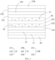
- FIG. 1 is a structural diagram of a display panel provided by an embodiment of the application.
- the display panel comprises a base substrate 10, an array layer 11 and a light-emitting device layer 12 stacked on the base substrate 10, sequentially.
- the light-emitting device layer 12 is provided with a plurality of light-emitting units
- the array layer 11 is provided with a plurality of pixel driving circuits for controlling and driving the light-emitting units to emit light.
- the pixel driving circuit is composed of a plurality of thin film transistors, capacitors, signal lines and scanning lines.
- the light-emitting unit comprises an organic light-emitting diode.
- the type of the light-emitting unit is not limited to the organic light-emitting diode in the foregoing embodiment, and may also be a micro light-emitting diode (Micro LED) or a mini light-emitting diode (Mini LED).
- the display panel further comprises an encapsulation layer 13, which is arranged on the light-emitting side of the light-emitting device layer 12 and covers the light-emitting device layer 12 to prevent water vapor and oxygen from intruding into the light-emitting device layer 12 to cause a light-emitting unit damaged.
- first scattering particles 14 are distributed in the encapsulation layer 13.
- the first scattering particles 14 are nanoparticles, and the refractive index of the first scattering particles 14 is different from the refractive index of the encapsulation layer 13, so that the first scattering particles 14 possess a refraction effect on the light irradiated to the interface between the first scattering particles 14 and the encapsulation layer 13.
- the refractive index of the encapsulation layer 13 can be adjusted to increase or decrease the emitting angle of the light emitted by the light-emitting device layer 12, thereby the viewing angle of the display panel can be improved.
- the encapsulation layer 13 comprises a first inorganic encapsulation layer 131, an organic encapsulation layer 132 and a second inorganic encapsulation layer.
- the first inorganic encapsulation layer 131 is arranged on the light-emitting side of the light-emitting device layer 12.
- the organic encapsulation layer 132 is arranged on a side of the first inorganic encapsulation layer away from the light-emitting device layer 12.
- the second inorganic encapsulation layer 133 is arranged on a side of the first inorganic encapsulation layer 131 away from the light-emitting device layer 12 and covers the organic encapsulation layer 132.
- the first inorganic encapsulation layer 131 is made of an inorganic transparent material, and the inorganic transparent material may comprise, but is not limited to, at least one of SiO, SiN, or SiON.
- the first inorganic encapsulation layer 131 may be prepared by plasma enhanced chemical vapor deposition (PECVD) or atomic layer deposition (ALD).
- the thickness of the first inorganic encapsulation layer 131 is 1 ⁇ m. In practical applications, the thickness of the first inorganic encapsulation layer 131 is not limited to 1 ⁇ m in the foregoing embodiment, and may also be 0.8 ⁇ m, 0.6 ⁇ m, 1.2 ⁇ m, 1.4 ⁇ m or the like.
- the organic encapsulation layer 132 is made of an organic transparent material, and the organic transparent material may comprise, but is not limited to, epoxy resin or acrylic material. In the actual preparation process, the organic encapsulation layer 132 may be prepared by inkjet printing, screen printing, electronic spraying or the like.
- the thickness of the organic encapsulation layer 132 is 10 ⁇ m. In practical applications, the thickness of the organic encapsulation layer 132 is not limited to 10 ⁇ m in the foregoing embodiment, and may also be 8 ⁇ m, 6 ⁇ m, 12 ⁇ m or 14 ⁇ m.
- the second inorganic encapsulation layer 133 is made of an inorganic transparent material, and the inorganic transparent material may comprise, but is not limited to, at least one of SiO, SiN, or SiON.
- the second inorganic encapsulation layer 133 can be prepared using the same material and the same preparation process as the first inorganic encapsulation layer 131.
- the first scattering particles 14 are distributed in the organic encapsulation layer 132.
- the first scattering particles 14 are made of nano-scale organic silicon materials.
- the material of the first scattering particles 14 is not limited to the nano-scale organic silicon materials in the foregoing embodiment, and can also be made of inorganic materials.
- the inorganic materials may comprise, but are not limited to, at least one or a mixture of SiNx, Si3N4, TiO2, MgO, ZnO, SnO2, Al2O3 and CaF2.
- the refractive index of the first scattering particles 14 is greater than the refractive index of the organic encapsulation layer 132.
- the light is mainly refracted at the interface between the organic encapsulation layer 132 and the first scattering particles 14.
- the incident angle of the light is greater than the refraction angle to make the light emitted by the light emitting device layer 12 converge toward the middle.
- the forward light extraction efficiency of the display panel can be improved, and the viewing angle of the display panel can be improved.
- the refractive index of the organic encapsulation layer 132 is greater than or equal to 1.45, and less than or equal to 1.55.
- the refractive index of the first scattering particles 14 is greater than or equal to 1.8, and less than or equal to 2.
- the refractive index of the organic encapsulation layer 132 may be 1.45, 1.5 or 1.55, etc..
- the refractive index of the first scattering particles 14 may be 1.8, 1.9, or 2.0, etc..
- the structure of the encapsulation layer 13 is not limited to the foregoing three-layer encapsulation structure formed by the first inorganic encapsulation layer 131, the organic encapsulation layer 132 and the second inorganic encapsulation layer 133, and can also be formed by interspersing and superimposing multilayer inorganic encapsulation layers and multilayer organic encapsulation layers.
- the first scattering particles 14 can be uniformly distributed in at least one organic encapsulation layer in the multilayer organic encapsulation layers.
- the display panel further comprises a barrier film 15, and the barrier film 15 is arranged on a side of the encapsulation layer 13 away from the light-emitting device layer 12 and covers the encapsulation layer 13.
- the barrier film 15 can further encapsulate the light-emitting device layer 12 and the array layer 11, and prevent water vapor and oxygen from intruding into the light-emitting device layer 12 and the array layer 11.
- the barrier film 15 comprises at least two antireflective layers 150 with different refractive indexes.
- the light transmittance of the barrier film 15 can be increased, thereby improving the light extraction efficiency of the display panel.
- the antireflective layers 150 comprises a first antireflective layer 151 and a second antireflective layer 152.
- the first antireflective layer 151 is arranged on a side of the encapsulation layer 13 away from the light-emitting device layer 12, and the second antireflective layer 152 is arranged on a side of the first antireflective layer 151 away from the encapsulation layer 13.
- the refractive index of the first antireflective layer 151 is greater than the refractive index of the second antireflective layer 152.
- the refractive index of the first antireflective layer 151 should be greater than or equal to 1.8, and the refractive index of the first antireflective layer 151 may specifically be 1.8, 1.9, 2.0 or the like.
- the refractive index of the second antireflective layer 152 should be greater than or equal to 1.3, and less than or equal to 1.6, and the refractive index of the second antireflective layer 152 may specifically be 1.3, 1.4, 1.5, 1.6 or the like.
- the first antireflective layer 151 may be made of transparent organic material or transparent inorganic material.
- the transparent organic material may comprise organosiloxane.
- the transparent inorganic material may comprise any one or a mixture of TiO2, ZrO2 or ZnO.
- the second antireflective layer 152 may be made of transparent organic material or inorganic material.
- the transparent organic material may comprise but is not limited to at least one of epoxy resin or polyacrylic resin.
- the transparent inorganic material may comprise SiOx.
- the barrier film 15 further comprises a barrier layer 153.
- the barrier layer 153 is arranged between the first antireflective layer 151 and the second antireflective layer 152.
- the barrier layer 153 may be formed on the first antireflective layer 151 by means of atomic layer deposition or sputtering.
- the refractive index of the barrier layer 153 is less than the refractive index of the first antireflective layer 151, and greater than the refractive index of the second antireflective layer 152.
- the barrier layer 153 is a high water barrier film layer, and the refractive index of the barrier layer 153 should be greater than or equal to 1.6, and less than or equal to 1.7.
- the refractive index of the barrier layer 153 may specifically be 1.6, 1.65, 1.7 or the like.
- the structure of the barrier film 15 is not limited to the laminated structure of the first antireflective layer 151, the barrier layer 153 and the second antireflective layer 152 that are sequentially stacked from bottom to top in the foregoing embodiment, but can also be a laminated structure in which three or more antireflective layers with different refractive indexes are alternately arranged. By alternately arranging the three or more antireflective layers with different refractive indexes, the light extraction efficiency of the display panel can also be adjusted.
- the barrier film 15 further comprises a protective layer 154.
- the protective layer 154 is arranged on the surface of the second antireflective layer 152 away from the barrier layer 153.
- the material of the protective layer 154 may comprise but not limited to PET, COP and PMMA.
- the display panel further comprises an adhesive layer 16.
- the adhesive layer 16 is arranged between the encapsulation layer 13 and the barrier film 15.
- the barrier film 15 is attached to the encapsulation layer 13 through the adhesive layer 16.
- second scattering particles 17 are distributed in the adhesive layer 16.
- the second scattering particles 17 are nanoparticles, and the refractive index of the second scattering particles 17 is greater than the refractive index of the adhesive layer 16, so that the second scattering particles 17 possess a refraction effect on the light irradiated to the interface between the second scattering particles 17 and the adhesive layer 16.
- the refractive index of the adhesive layer 16 can be increased, so that the large-angle light emitted by the light-emitting device layer 12 is further converged to the middle, thereby improving the forward light extraction efficiency of the display panel and improving the viewing angle of the display panel.
- the refractive index of the adhesive layer 16 is less than the refractive index of the first antireflective layer 151.
- the adhesive layer 16 may be pressure sensitive adhesive (PSA) or optical adhesive.
- PSA pressure sensitive adhesive
- the refractive index of the adhesive layer 16 should be greater than or equal to 1.45, and less than or equal to 1.5.
- the refractive index of the adhesive layer 16 may specifically be 1.45, 1.47, 1.49, 1.5 or the like.
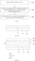
- FIG. 2 is a flowchart of a manufacturing method of a display panel provided by an embodiment of the application.
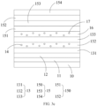
- FIG. 3a to FIG. 3c are flowcharts of a manufacturing method of a display panel provided by an embodiment of the application.
- the manufacturing method of the display panel is employed to manufacture the display panel in the foregoing embodiment.
- the manufacturing method of the display panel comprises:
- Step S10 forming a light-emitting device layer 12.
- the light-emitting device layer 12 is formed on a side of the base substrate 10.
- a plurality of light-emitting units are provided in the light-emitting device layer 12, and the light-emitting unit comprises an organic light-emitting diode.
- a plurality of pixel openings can be formed first by etching the pixel defining layer in the light-emitting device layer 12.
- a light-emitting layer is formed in the pixel opening by evaporation or inkjet printing, and then a corresponding electrode is deposited on the light-emitting layer by physical vapor deposition or sputtering.
- the material of the electrode may comprise, but is not limited to, Al or Ag.
- an array layer 11 Before forming the light-emitting device layer 12 on the base substrate 10, an array layer 11 should also be formed on the base substrate 10.
- the array layer 11 is provided with a plurality of pixel driving circuits for controlling and driving the light-emitting unit to emit light.
- the pixel driving circuit is composed of a plurality of thin film transistors, capacitors, signal lines and scanning lines.
- Step S20 forming an encapsulation layer 13 on a light-emitting side of the light-emitting device layer 12 and covering the light-emitting device layer 12.
- first scattering particles 14 are distributed in the encapsulation layer 13.
- the first scattering particles 14 possess light scattering effect, and the light will be refracted when passing through the first scattering particles 14 from the encapsulation layer 13, so that the light is emitted from the first scattering particles 14 with a larger angle.
- the emitting angle of the light can be increased, so that the viewing angle of the display panel can be improved.
- Step S20 the step of forming the encapsulation layer 13 on the light-emitting side of the light-emitting device layer 12 and covering the light-emitting device layer 12 comprises:
- Step S201 forming a first inorganic encapsulation layer 131 on the light-emitting side of the light-emitting device layer 12;
- Step S202 forming an organic encapsulation layer 132 on a side of the first inorganic encapsulation layer 131 away from the light-emitting device layer 12;
- Step S203 forming a second inorganic encapsulation layer 133 at a side of the first inorganic encapsulation layer 131 away from the light-emitting device layer 12, wherein the second inorganic encapsulation layer 133 covers the organic encapsulation layer 132;
- the first inorganic encapsulation layer can be formed by using an inorganic transparent material through plasma-enhanced chemical vapor deposition or atomic layer deposition.
- the first inorganic encapsulation layer is made of an inorganic transparent material, and the inorganic transparent material may comprise, but is not limited to, at least one of SiO, SiN, or SiON.
- the thickness of the first inorganic encapsulation layer 131 is 1 ⁇ m. In practical applications, the thickness of the first inorganic encapsulation layer 131 is not limited to 1 ⁇ m in the foregoing embodiment, and may also be 0.8 ⁇ m, 0.6 ⁇ m, 1.2 ⁇ m, 1.4 ⁇ m or the like.
- the organic encapsulation layer 132 may be prepared by using organic transparent materials through inkjet printing, screen printing, electronic spraying, etc.
- the organic transparent material may comprise, but is not limited to, epoxy resin or acrylic material.
- the thickness of the organic encapsulation layer 132 is 10 u m. In practical applications, the thickness of the organic encapsulation layer 132 is not limited to 10 ⁇ m in the foregoing embodiment, and may also be 8 ⁇ m, 6 ⁇ m, 12 ⁇ m or 14 ⁇ m.
- the first scattering particles 14 are distributed in the organic encapsulation layer 132.
- the refractive index of the first scattering particles 14 is greater than the refractive index of the organic encapsulation layer 132.
- the first scattering particles 14 are made of nano-scale organic silicon materials.
- the material of the first scattering particles 14 is not limited to the nano-scale organic silicon materials in the foregoing embodiment, and can also be made of inorganic materials.
- the inorganic materials may comprise, but are not limited to, at least one or a mixture of SiNx, Si3N4, TiO2, MgO, ZnO, SnO2, Al2O3 and CaF2.
- the second inorganic encapsulation layer 133 is made of an inorganic transparent material, and the inorganic transparent material may comprise, but is not limited to, at least one of SiO, SiN, or SiON. In the actual preparation process, the second inorganic encapsulation layer 133 can be prepared using the same material and the same preparation process as the first inorganic encapsulation layer 131.
- the refractive index of the first scattering particles 14 is greater than the refractive index of the organic encapsulation layer 132.
- the light is mainly refracted at the interface between the organic encapsulation layer 132 and the first scattering particles 14.
- the incident angle of the light is greater than the refraction angle to make the light emitted by the light emitting device layer 12 converge toward the middle.
- the forward light extraction efficiency of the display panel can be improved, and the viewing angle of the display panel can be improved.
- the refractive index of the organic encapsulation layer 132 is greater than or equal to 1.45, and less than or equal to 1.55.
- the refractive index of the first scattering particles 14 is greater than or equal to 1.8, and less than or equal to 2.
- the refractive index of the organic encapsulation layer 132 may be 1.45, 1.5 or 1.55, etc..
- the refractive index of the first scattering particles 14 may be 1.8, 1.9, or 2.0, etc..
- the structure of the encapsulation layer 13 is not limited to the foregoing three-layer encapsulation structure formed by the first inorganic encapsulation layer 131, the organic encapsulation layer 132 and the second inorganic encapsulation layer 133, and can also be formed by interspersing and superimposing multilayer inorganic encapsulation layers and multilayer organic encapsulation layers.
- the first scattering particles 14 can be uniformly distributed in at least one organic encapsulation layer in the multilayer organic encapsulation layers.
- Step S30 forming a barrier film 15 on a side of the encapsulation layer 13 away from the light-emitting device layer 12.
- the barrier film 15 comprises at least two antireflective layers with different refractive indexes.
- the light transmittance of the barrier film 15 can be increased, thereby improving the display result of the display panel.
- the step of forming the barrier film 15 on the side of the encapsulation layer 13 away from the light-emitting device layer 12 comprises: forming a first antireflective layer 151 on a side of the encapsulation layer 13 away from the light-emitting device layer 12; and forming a second antireflective layer 152 on a side of the first antireflective layer 151 away from the encapsulation layer 13.
- the first antireflective layer 151 may be made of transparent organic material or transparent inorganic material.
- the transparent organic material may comprise organosiloxane.
- the transparent inorganic material may comprise any one or a mixture of TiO2, ZrO2 or ZnO.
- the second antireflective layer 152 may be made of transparent organic material or inorganic material.
- the transparent organic material may comprise but is not limited to at least one of epoxy resin or polyacrylic resin.
- the transparent inorganic material may comprise SiOx.
- the refractive index of the first antireflective layer 151 should be greater than or equal to 1.8, and the refractive index of the first antireflective layer 151 may specifically be 1.8, 1.9, 2.0 or the like.
- the refractive index of the second antireflective layer 152 should be greater than or equal to 1.3, and less than or equal to 1.6, and the refractive index of the second antireflective layer 152 may specifically be 1.3, 1.4, 1.5, 1.6 or the like.
- Step S30 the step of forming the barrier film 15 on the side of the encapsulation layer 13 away from the light-emitting device layer 12 further comprises:
- barrier layer 153 on the side of the first antireflective layer 151 away from the encapsulation layer 13 before forming the second antireflective layer 152;
- the second antireflective layer 152 on a side of the barrier layer 153 away from the first antireflective layer 151.
- the barrier layer 153 may be formed on the first antireflective layer 151 by means of atomic layer deposition or sputtering.
- the refractive index of the barrier layer 153 is less than the refractive index of the first antireflective layer 151, and greater than the refractive index of the second antireflective layer 152.
- the barrier layer 153 is a high water barrier film layer, and the refractive index of the barrier layer 153 should be greater than or equal to 1.6, and less than or equal to 1.7.
- the refractive index of the barrier layer 153 may specifically be 1.6, 1.65, 1.7 or the like.
- the structure of the barrier film 15 is not limited to the laminated structure of the first antireflective layer 151, the barrier layer 153 and the second antireflective layer 152 that are sequentially stacked from bottom to top in the foregoing embodiment, but can also be a laminated structure in which three or more antireflective layers with different refractive indexes are alternately arranged. By alternately arranging the three or more antireflective layers with different refractive indexes, the light extraction efficiency of the display panel can also be adjusted.
- the step of forming the barrier film 15 on the side of the encapsulation layer 13 away from the light-emitting device layer 12 further comprises: adhering the side of the first antireflective layer 151 away from the barrier layer 153 with the side of the encapsulation layer 13 away from the light-emitting device layer 12 through an adhesive layer 16.
- second scattering particles 17 are distributed in the adhesive layer 16.
- the refractive index of the second scattering particles 17 is greater than the refractive index of the adhesive layer 16.
- the light is refracted when passing through the second scattering particles 17 from the adhesive layer 16, so that the light is emitted from the second scattering particles 17 at a larger angle.
- the emitting angle of the light can be increased, so that the viewing angle of the display panel can be improved.
- the refractive index of the adhesive layer 16 is less than the refractive index of the first antireflective layer 151.
- the refractive index of the adhesive layer 16 is 1.5. In practical applications, the refractive index of the adhesive layer 16 is not limited to 1.5 in the foregoing embodiment, but can also be 1.45, 1.47, or 1.49, etc., and only needs to be greater than or equal to 1.45, and less than or equal to 1.5.
- the embodiment of the present application provides a display panel, a manufacturing method, and an electronic device.
- the display panel comprises a light-emitting device layer, an encapsulation layer and a barrier film.
- the encapsulation layer is arranged on a light-emitting side of the light-emitting device layer and covers the light-emitting device layer.
- the barrier film is arranged on a side of the encapsulation layer away from the light-emitting device layer.
- First scattering particles are distributed in the encapsulation layer, and the light scattering effect of the first scattering particles on the light-emitting device layer can be employed to improve the viewing angle of the display panel.
- the barrier film comprises at least two antireflective layers with different refractive indexes. to increase the transmittance of the barrier film, thereby improving the light extraction efficiency of the display panel.
Landscapes
- Physics & Mathematics (AREA)
- Optics & Photonics (AREA)
- Engineering & Computer Science (AREA)
- Manufacturing & Machinery (AREA)
- Electroluminescent Light Sources (AREA)
- Devices For Indicating Variable Information By Combining Individual Elements (AREA)
- Surface Treatment Of Optical Elements (AREA)
- Laminated Bodies (AREA)
Abstract
Description
- The present application relates to a display field, and more particularly to a display panel, a manufacturing method and an electronic device.
- In recent years, the development of Organic Light Emitting Diode (OLED) display technology has advanced by leaps and bounds. Organic Light Emitting Diode (OLED) display panels have received more and more attention due to their advantages of lightness and thinness, fast response, wide viewing angle, high contrast and flexibility. They are mainly employed in display fields such as mobile phones, flat panels and televisions.
- Organic light-emitting diode display panels can be categorized into top-emission type, bottom-emission type and penetration type according to the light-emitting mode of OLED devices. The top-emission type uses top-emission light. Regardless of the shape of the circuit on the substrate, it possesses no direct effect on the light extraction efficiency of the OLED device, making the top-emission type more efficient than the bottom-emission type and has become the mainstream design method of the current organic light emitting diode display panel. However, in the process of light propagation of the top-emission organic light-emitting diode display panel, due to the mismatch of the refractive index between the various layers of the display panel, a part of the emitted photons will be trapped in the panel due to the waveguide effect. The maximum light extraction cannot be achieved, resulting in low light extraction efficiency of the display panel.
- In summary, there is a problem of low light extraction efficiency in the existing top-emitting organic light-emitting diode display panel. Therefore, there is a need to provide a display panel, a manufacturing method and an electronic device to solve the existing problems of the prior art.
- The embodiment of the present application provides a display panel, a manufacturing method and an electronic device, which are employed to solve the problem of low light extraction efficiency in the existing top-emitting organic light-emitting diode display panel.
- The embodiment of the present application provides a display panel, comprising:
- a light-emitting device layer;
- an encapsulation layer being arranged on a light-emitting side of the light-emitting device layer and covering the light-emitting device layer; and
- a barrier film arranged on a side of the encapsulation layer away from the light-emitting device layer;
- wherein first scattering particles are distributed in the encapsulation layer, and the barrier film comprises at least two antireflective layers with different refractive indexes.
- According to one embodiment of the present application, the thin film encapsulation layer comprises:
- a first inorganic encapsulation layer arranged on the light-emitting side of the light-emitting device layer;
- an organic encapsulation layer arranged on a side of the first inorganic encapsulation layer away from the light-emitting device layer; and
- a second inorganic encapsulation layer being arranged at a side of the first inorganic encapsulation layer and covering the organic encapsulation layer;
- wherein the first scattering particles are distributed in the organic encapsulation layer.
- According to one embodiment of the present application, a refractive index of the first scattering particles is greater than a refractive index of the organic encapsulation layer.
- According to one embodiment of the present application, the antireflective layers comprise:
- a first antireflective layer arranged on the side of the encapsulation layer away from the light-emitting device layer; and
- a second antireflective layer arranged on a side of first antireflective layer away from the encapsulation layer;
- wherein the refractive index of the first antireflective layer is greater than the refractive index of the second antireflective layer.
- According to one embodiment of the present application, the refractive index of the first antireflective layer is greater than or equal to 1.8, and the refractive index of the second antireflective layer is greater than or equal to 1.3, and less than or equal to 1.6.
- According to one embodiment of the present application, the barrier film further comprises a barrier layer arranged between the first antireflective layer and the second antireflective layer;
wherein a refractive index of the barrier layer is less than the refractive index of the first antireflective layer, and is greater than the refractive index of the second antireflective layer. - According to one embodiment of the present application, the display panel further comprises an adhesive layer arranged between the encapsulation layer and the barrier film;
wherein second scattering particles are distributed in the adhesive layer. - According to one embodiment of the present application, a refractive index of the adhesive layer is less than the refractive index of the first antireflective layer.
- According to one embodiment of the present application, a refractive index of the second scattering particles is greater than the refractive index of the adhesive layer.
- The embodiment of the present application further provides an electronic device, comprising a display panel, wherein the display panel comprises:
- a light-emitting device layer;
- an encapsulation layer being arranged on a light-emitting side of the light-emitting device layer and covering the light-emitting device layer; and
- a barrier film arranged on a side of the encapsulation layer away from the light-emitting device layer;
- wherein first scattering particles are distributed in the encapsulation layer, and the barrier film comprises at least two antireflective layers with different refractive indexes.
- According to one embodiment of the present application, the thin film encapsulation layer comprises:
- a first inorganic encapsulation layer arranged on the light-emitting side of the light-emitting device layer;
- an organic encapsulation layer arranged on a side of the first inorganic encapsulation layer away from the light-emitting device layer; and
- a second inorganic encapsulation layer being arranged at a side of the first inorganic encapsulation layer and covering the organic encapsulation layer;
- wherein the first scattering particles are distributed in the organic encapsulation layer.
- According to one embodiment of the present application, a refractive index of the first scattering particles is greater than a refractive index of the organic encapsulation layer.
- According to one embodiment of the present application, the antireflective layers comprise:
- a first antireflective layer arranged on the side of the encapsulation layer away from the light-emitting device layer; and
- a second antireflective layer arranged on a side of first antireflective layer away from the encapsulation layer;
- wherein the refractive index of the first antireflective layer is greater than the refractive index of the second antireflective layer.
- According to one embodiment of the present application, the refractive index of the first antireflective layer is greater than or equal to 1.8, and the refractive index of the second antireflective layer is greater than or equal to 1.3, and less than or equal to 1.6.
- The embodiment of the present application further provides a manufacturing method of a display panel, employed to manufacture the aforesaid display panel, wherein the manufacturing method of the display panel comprises:
- forming a light-emitting device layer;
- forming an encapsulation layer on a light-emitting side of the light-emitting device layer and covering the light-emitting device layer; and
- forming a barrier film on a side of the encapsulation layer away from the light-emitting device layer;
- wherein first scattering particles are distributed in the encapsulation layer, and the barrier film comprises at least two antireflective layers with different refractive indexes.
- According to one embodiment of the present application, the step of forming the encapsulation layer on the light-emitting side of the light-emitting device layer and covering the light-emitting device layer comprises:
- forming a first inorganic encapsulation layer on the light-emitting side of the light-emitting device layer;
- forming an organic encapsulation layer on a side of the first inorganic encapsulation layer away from the light-emitting device layer; and
- forming a second inorganic encapsulation layer at a side of the first inorganic encapsulation layer and covering the organic encapsulation layer;
- wherein the first scattering particles are distributed in the organic encapsulation layer.
- According to one embodiment of the present application, a refractive index of the first scattering particles is greater than a refractive index of the organic encapsulation layer.
- According to one embodiment of the present application, the step of forming the barrier film on the side of the encapsulation layer away from the light-emitting device layer comprises:
- forming a first antireflective layer; and
- forming a second antireflective layer on a side of the first antireflective layer;
- wherein the refractive index of the first antireflective layer is greater than the refractive index of the second antireflective layer.
- According to one embodiment of the present application, the step of forming the barrier film on the side of the encapsulation layer away from the light-emitting device layer further comprises:
- forming a barrier layer on the side of the first antireflective layer before forming the second antireflective layer; and
- forming the second antireflective layer on a side of the barrier layer away from the first antireflective layer;
- wherein a refractive index of the barrier layer is less than the refractive index of the first antireflective layer, and is greater than the refractive index of the second antireflective layer.
- According to one embodiment of the present application, the step of forming the barrier film on the side of the encapsulation layer away from the light-emitting device layer further comprises:
- adhering the side of the first antireflective layer away from the barrier layer with the side of the encapsulation layer away from the light-emitting device layer through an adhesive layer;
- wherein second scattering particles are distributed in the adhesive layer.
- The benefits of the embodiment of the present application are: the embodiment of the present application provides a display panel, a manufacturing method, and an electronic device. The display panel comprises a light-emitting device layer, an encapsulation layer and a barrier film. The encapsulation layer is arranged on a light-emitting side of the light-emitting device layer and covers the light-emitting device layer. The barrier film is arranged on a side of the encapsulation layer away from the light-emitting device layer. First scattering particles are distributed in the encapsulation layer, and the light scattering effect of the first scattering particles on the light-emitting device layer can be employed to improve the viewing angle of the display panel. The barrier film comprises at least two antireflective layers with different refractive indexes. to increase the transmittance of the barrier film, thereby improving the light extraction efficiency of the display panel.
- In order to more clearly illustrate the embodiments of the present application and the prior art, the following figures will be described in the embodiments and the prior art are briefly introduced. It is obvious that the drawings are only some embodiments of the present application, those of ordinary skill in this field can obtain other figures according to these figures without paying the premise.
-
FIG. 1 is a structural diagram of a display panel provided by an embodiment of the application; -
FIG. 2 is a flowchart of a manufacturing method of a display panel provided by an embodiment of the application; -
FIG. 3a to FIG. 3c are flowcharts of a manufacturing method of a display panel provided by an embodiment of the application. - The following descriptions for the respective embodiments are specific embodiments capable of being implemented for illustrations of the present application with referring to appended figures. The terms of up, down, front, rear, left, right, interior, exterior, side, etcetera mentioned in the present application are merely directions of referring to appended figures. Thus, the used directional terms are used to describe and understand the present application, but the present invention is not limited thereto. In the figure, units with similar structures are denoted by the same reference numerals.
- The present application will be further described in detail with the accompanying drawings and the specific embodiments.
- The embodiment of the present application provides a display panel and an electronic device. The electronic device comprises the display panel, a housing for carrying the display panel, and components such as a processor and a power supply arranged in the housing for driving the display panel to realize a screen display function. The electronic device may be a mobile terminal, such as a smart phone, a tablet computer, a notebook computer, etc.. The electronic device may also be a wearable terminal, such as a smart watch, a smart bracelet, smart glasses, an augmented reality device, etc.. The electronic device may also be a fixed terminal, such as a desktop computer, a television, etc..
- As shown in
FIG. 1, FIG. 1 is a structural diagram of a display panel provided by an embodiment of the application. The display panel comprises abase substrate 10, anarray layer 11 and a light-emittingdevice layer 12 stacked on thebase substrate 10, sequentially. The light-emittingdevice layer 12 is provided with a plurality of light-emitting units, and thearray layer 11 is provided with a plurality of pixel driving circuits for controlling and driving the light-emitting units to emit light. The pixel driving circuit is composed of a plurality of thin film transistors, capacitors, signal lines and scanning lines. - In the embodiment of the present application, the light-emitting unit comprises an organic light-emitting diode. In practical applications, the type of the light-emitting unit is not limited to the organic light-emitting diode in the foregoing embodiment, and may also be a micro light-emitting diode (Micro LED) or a mini light-emitting diode (Mini LED).
- The display panel further comprises an
encapsulation layer 13, which is arranged on the light-emitting side of the light-emittingdevice layer 12 and covers the light-emittingdevice layer 12 to prevent water vapor and oxygen from intruding into the light-emittingdevice layer 12 to cause a light-emitting unit damaged. - Furthermore,
first scattering particles 14 are distributed in theencapsulation layer 13. Thefirst scattering particles 14 are nanoparticles, and the refractive index of thefirst scattering particles 14 is different from the refractive index of theencapsulation layer 13, so that thefirst scattering particles 14 possess a refraction effect on the light irradiated to the interface between thefirst scattering particles 14 and theencapsulation layer 13. By controlling the content or mass ratio of thefirst scattering particles 14 in theencapsulation layer 13, the refractive index of theencapsulation layer 13 can be adjusted to increase or decrease the emitting angle of the light emitted by the light-emittingdevice layer 12, thereby the viewing angle of the display panel can be improved. - In the embodiment of the present application, as shown in
FIG. 1 , theencapsulation layer 13 comprises a firstinorganic encapsulation layer 131, anorganic encapsulation layer 132 and a second inorganic encapsulation layer. The firstinorganic encapsulation layer 131 is arranged on the light-emitting side of the light-emittingdevice layer 12. Theorganic encapsulation layer 132 is arranged on a side of the first inorganic encapsulation layer away from the light-emittingdevice layer 12. The secondinorganic encapsulation layer 133 is arranged on a side of the firstinorganic encapsulation layer 131 away from the light-emittingdevice layer 12 and covers theorganic encapsulation layer 132. - Specifically, the first
inorganic encapsulation layer 131 is made of an inorganic transparent material, and the inorganic transparent material may comprise, but is not limited to, at least one of SiO, SiN, or SiON. In the actual preparation process, the firstinorganic encapsulation layer 131 may be prepared by plasma enhanced chemical vapor deposition (PECVD) or atomic layer deposition (ALD). - In the embodiment of the present application, the thickness of the first
inorganic encapsulation layer 131 is 1 µm. In practical applications, the thickness of the firstinorganic encapsulation layer 131 is not limited to 1 µ m in the foregoing embodiment, and may also be 0.8 µm, 0.6 µm, 1.2 µm, 1.4 µm or the like. - The
organic encapsulation layer 132 is made of an organic transparent material, and the organic transparent material may comprise, but is not limited to, epoxy resin or acrylic material. In the actual preparation process, theorganic encapsulation layer 132 may be prepared by inkjet printing, screen printing, electronic spraying or the like. - In the embodiment of the present application, the thickness of the
organic encapsulation layer 132 is 10 µm. In practical applications, the thickness of theorganic encapsulation layer 132 is not limited to 10 µm in the foregoing embodiment, and may also be 8 µm, 6 µm, 12 µm or 14 µm. - Specifically, the second
inorganic encapsulation layer 133 is made of an inorganic transparent material, and the inorganic transparent material may comprise, but is not limited to, at least one of SiO, SiN, or SiON. In the actual preparation process, the secondinorganic encapsulation layer 133 can be prepared using the same material and the same preparation process as the firstinorganic encapsulation layer 131. - As shown in
FIG. 1 , thefirst scattering particles 14 are distributed in theorganic encapsulation layer 132. - In the embodiment of the present application, the
first scattering particles 14 are made of nano-scale organic silicon materials. In practical applications, the material of thefirst scattering particles 14 is not limited to the nano-scale organic silicon materials in the foregoing embodiment, and can also be made of inorganic materials. The inorganic materials may comprise, but are not limited to, at least one or a mixture of SiNx, Si3N4, TiO2, MgO, ZnO, SnO2, Al2O3 and CaF2. - Furthermore, the refractive index of the
first scattering particles 14 is greater than the refractive index of theorganic encapsulation layer 132. The light is mainly refracted at the interface between theorganic encapsulation layer 132 and thefirst scattering particles 14. When light enters the firstreflective particle 14 from theorganic encapsulation layer 132, since the refractive index of thefirst scattering particle 14 is greater than the refractive index of theorganic encapsulation layer 132, the incident angle of the light is greater than the refraction angle to make the light emitted by the light emittingdevice layer 12 converge toward the middle. Thus, the forward light extraction efficiency of the display panel can be improved, and the viewing angle of the display panel can be improved. - In the embodiment of the present application, the refractive index of the
organic encapsulation layer 132 is greater than or equal to 1.45, and less than or equal to 1.55. The refractive index of thefirst scattering particles 14 is greater than or equal to 1.8, and less than or equal to 2. Specifically, the refractive index of theorganic encapsulation layer 132 may be 1.45, 1.5 or 1.55, etc.. The refractive index of thefirst scattering particles 14 may be 1.8, 1.9, or 2.0, etc.. - It should be noted that the structure of the
encapsulation layer 13 is not limited to the foregoing three-layer encapsulation structure formed by the firstinorganic encapsulation layer 131, theorganic encapsulation layer 132 and the secondinorganic encapsulation layer 133, and can also be formed by interspersing and superimposing multilayer inorganic encapsulation layers and multilayer organic encapsulation layers. Thefirst scattering particles 14 can be uniformly distributed in at least one organic encapsulation layer in the multilayer organic encapsulation layers. - The display panel further comprises a
barrier film 15, and thebarrier film 15 is arranged on a side of theencapsulation layer 13 away from the light-emittingdevice layer 12 and covers theencapsulation layer 13. Thebarrier film 15 can further encapsulate the light-emittingdevice layer 12 and thearray layer 11, and prevent water vapor and oxygen from intruding into the light-emittingdevice layer 12 and thearray layer 11. - Furthermore, the
barrier film 15 comprises at least twoantireflective layers 150 with different refractive indexes. By using the difference in refractive indexes of at least twoantireflective layers 150, the light transmittance of thebarrier film 15 can be increased, thereby improving the light extraction efficiency of the display panel. - As shown in
FIG. 1 , theantireflective layers 150 comprises a firstantireflective layer 151 and a secondantireflective layer 152. The firstantireflective layer 151 is arranged on a side of theencapsulation layer 13 away from the light-emittingdevice layer 12, and the secondantireflective layer 152 is arranged on a side of the firstantireflective layer 151 away from theencapsulation layer 13. The refractive index of the firstantireflective layer 151 is greater than the refractive index of the secondantireflective layer 152. - In the embodiment of the present application, the refractive index of the first
antireflective layer 151 should be greater than or equal to 1.8, and the refractive index of the firstantireflective layer 151 may specifically be 1.8, 1.9, 2.0 or the like. The refractive index of the secondantireflective layer 152 should be greater than or equal to 1.3, and less than or equal to 1.6, and the refractive index of the secondantireflective layer 152 may specifically be 1.3, 1.4, 1.5, 1.6 or the like. - The first
antireflective layer 151 may be made of transparent organic material or transparent inorganic material. The transparent organic material may comprise organosiloxane. The transparent inorganic material may comprise any one or a mixture of TiO2, ZrO2 or ZnO. - The second
antireflective layer 152 may be made of transparent organic material or inorganic material. The transparent organic material may comprise but is not limited to at least one of epoxy resin or polyacrylic resin. The transparent inorganic material may comprise SiOx. - In the embodiment of the present application, the
barrier film 15 further comprises abarrier layer 153. Thebarrier layer 153 is arranged between the firstantireflective layer 151 and the secondantireflective layer 152. Thebarrier layer 153 may be formed on the firstantireflective layer 151 by means of atomic layer deposition or sputtering. - Furthermore, the refractive index of the
barrier layer 153 is less than the refractive index of the firstantireflective layer 151, and greater than the refractive index of the secondantireflective layer 152. - In the embodiment of the present application, the
barrier layer 153 is a high water barrier film layer, and the refractive index of thebarrier layer 153 should be greater than or equal to 1.6, and less than or equal to 1.7. The refractive index of thebarrier layer 153 may specifically be 1.6, 1.65, 1.7 or the like. - In practical applications, the structure of the
barrier film 15 is not limited to the laminated structure of the firstantireflective layer 151, thebarrier layer 153 and the secondantireflective layer 152 that are sequentially stacked from bottom to top in the foregoing embodiment, but can also be a laminated structure in which three or more antireflective layers with different refractive indexes are alternately arranged. By alternately arranging the three or more antireflective layers with different refractive indexes, the light extraction efficiency of the display panel can also be adjusted. - Furthermore, the
barrier film 15 further comprises aprotective layer 154. Theprotective layer 154 is arranged on the surface of the secondantireflective layer 152 away from thebarrier layer 153. The material of theprotective layer 154 may comprise but not limited to PET, COP and PMMA. - In the embodiment of the present application, the display panel further comprises an
adhesive layer 16. Theadhesive layer 16 is arranged between theencapsulation layer 13 and thebarrier film 15. Thebarrier film 15 is attached to theencapsulation layer 13 through theadhesive layer 16. - Furthermore,
second scattering particles 17 are distributed in theadhesive layer 16. Thesecond scattering particles 17 are nanoparticles, and the refractive index of thesecond scattering particles 17 is greater than the refractive index of theadhesive layer 16, so that thesecond scattering particles 17 possess a refraction effect on the light irradiated to the interface between thesecond scattering particles 17 and theadhesive layer 16. By adding thesecond scattering particles 17 to theadhesive layer 16, the refractive index of theadhesive layer 16 can be increased, so that the large-angle light emitted by the light-emittingdevice layer 12 is further converged to the middle, thereby improving the forward light extraction efficiency of the display panel and improving the viewing angle of the display panel. - Furthermore, the refractive index of the
adhesive layer 16 is less than the refractive index of the firstantireflective layer 151. - In the embodiment of the present application, the
adhesive layer 16 may be pressure sensitive adhesive (PSA) or optical adhesive. The refractive index of theadhesive layer 16 should be greater than or equal to 1.45, and less than or equal to 1.5. The refractive index of theadhesive layer 16 may specifically be 1.45, 1.47, 1.49, 1.5 or the like. - As shown in
FIG. 2 and FIG. 3a toFIG. 3c ,FIG. 2 is a flowchart of a manufacturing method of a display panel provided by an embodiment of the application.FIG. 3a to FIG. 3c are flowcharts of a manufacturing method of a display panel provided by an embodiment of the application. The manufacturing method of the display panel is employed to manufacture the display panel in the foregoing embodiment. The manufacturing method of the display panel comprises: - Step S10: forming a light-emitting
device layer 12. - As shown in
FIG. 3a , in Step S10, the light-emittingdevice layer 12 is formed on a side of thebase substrate 10. A plurality of light-emitting units are provided in the light-emittingdevice layer 12, and the light-emitting unit comprises an organic light-emitting diode. When preparing and forming the light-emittingdevice layer 12, a plurality of pixel openings can be formed first by etching the pixel defining layer in the light-emittingdevice layer 12. A light-emitting layer is formed in the pixel opening by evaporation or inkjet printing, and then a corresponding electrode is deposited on the light-emitting layer by physical vapor deposition or sputtering. The material of the electrode may comprise, but is not limited to, Al or Ag. - Before forming the light-emitting
device layer 12 on thebase substrate 10, anarray layer 11 should also be formed on thebase substrate 10. Thearray layer 11 is provided with a plurality of pixel driving circuits for controlling and driving the light-emitting unit to emit light. The pixel driving circuit is composed of a plurality of thin film transistors, capacitors, signal lines and scanning lines. - Step S20: forming an
encapsulation layer 13 on a light-emitting side of the light-emittingdevice layer 12 and covering the light-emittingdevice layer 12. - As shown in
FIG. 3b ,first scattering particles 14 are distributed in theencapsulation layer 13. Thefirst scattering particles 14 possess light scattering effect, and the light will be refracted when passing through thefirst scattering particles 14 from theencapsulation layer 13, so that the light is emitted from thefirst scattering particles 14 with a larger angle. Thus, the emitting angle of the light can be increased, so that the viewing angle of the display panel can be improved. - Furthermore, as shown in
FIG. 3b , in Step S20, the step of forming theencapsulation layer 13 on the light-emitting side of the light-emittingdevice layer 12 and covering the light-emittingdevice layer 12 comprises: - Step S201: forming a first
inorganic encapsulation layer 131 on the light-emitting side of the light-emittingdevice layer 12; - Step S202: forming an
organic encapsulation layer 132 on a side of the firstinorganic encapsulation layer 131 away from the light-emittingdevice layer 12; and - Step S203: forming a second
inorganic encapsulation layer 133 at a side of the firstinorganic encapsulation layer 131 away from the light-emittingdevice layer 12, wherein the secondinorganic encapsulation layer 133 covers theorganic encapsulation layer 132; - in Step S201, the first inorganic encapsulation layer can be formed by using an inorganic transparent material through plasma-enhanced chemical vapor deposition or atomic layer deposition. The first inorganic encapsulation layer is made of an inorganic transparent material, and the inorganic transparent material may comprise, but is not limited to, at least one of SiO, SiN, or SiON.
- In the embodiment of the present application, the thickness of the first
inorganic encapsulation layer 131 is 1 µm. In practical applications, the thickness of the firstinorganic encapsulation layer 131 is not limited to 1 µm in the foregoing embodiment, and may also be 0.8 µm, 0.6 µm, 1.2 µm, 1.4 µm or the like. - In Step S202, the
organic encapsulation layer 132 may be prepared by using organic transparent materials through inkjet printing, screen printing, electronic spraying, etc.. The organic transparent material may comprise, but is not limited to, epoxy resin or acrylic material. - In the embodiment of the present application, the thickness of the
organic encapsulation layer 132 is 10 u m. In practical applications, the thickness of theorganic encapsulation layer 132 is not limited to 10 µm in the foregoing embodiment, and may also be 8 µm, 6 µm, 12 µm or 14 µm. - In the embodiment of the present application, the
first scattering particles 14 are distributed in theorganic encapsulation layer 132. The refractive index of thefirst scattering particles 14 is greater than the refractive index of theorganic encapsulation layer 132. - The
first scattering particles 14 are made of nano-scale organic silicon materials. In practical applications, the material of thefirst scattering particles 14 is not limited to the nano-scale organic silicon materials in the foregoing embodiment, and can also be made of inorganic materials. The inorganic materials may comprise, but are not limited to, at least one or a mixture of SiNx, Si3N4, TiO2, MgO, ZnO, SnO2, Al2O3 and CaF2. - The second
inorganic encapsulation layer 133 is made of an inorganic transparent material, and the inorganic transparent material may comprise, but is not limited to, at least one of SiO, SiN, or SiON. In the actual preparation process, the secondinorganic encapsulation layer 133 can be prepared using the same material and the same preparation process as the firstinorganic encapsulation layer 131. - Furthermore, the refractive index of the
first scattering particles 14 is greater than the refractive index of theorganic encapsulation layer 132. The light is mainly refracted at the interface between theorganic encapsulation layer 132 and thefirst scattering particles 14. When light enters the firstreflective particle 14 from theorganic encapsulation layer 132, since the refractive index of thefirst scattering particle 14 is greater than the refractive index of theorganic encapsulation layer 132, the incident angle of the light is greater than the refraction angle to make the light emitted by the light emittingdevice layer 12 converge toward the middle. Thus, the forward light extraction efficiency of the display panel can be improved, and the viewing angle of the display panel can be improved. - In the embodiment of the present application, the refractive index of the
organic encapsulation layer 132 is greater than or equal to 1.45, and less than or equal to 1.55. The refractive index of thefirst scattering particles 14 is greater than or equal to 1.8, and less than or equal to 2. Specifically, the refractive index of theorganic encapsulation layer 132 may be 1.45, 1.5 or 1.55, etc.. The refractive index of thefirst scattering particles 14 may be 1.8, 1.9, or 2.0, etc.. - It should be noted that the structure of the
encapsulation layer 13 is not limited to the foregoing three-layer encapsulation structure formed by the firstinorganic encapsulation layer 131, theorganic encapsulation layer 132 and the secondinorganic encapsulation layer 133, and can also be formed by interspersing and superimposing multilayer inorganic encapsulation layers and multilayer organic encapsulation layers. Thefirst scattering particles 14 can be uniformly distributed in at least one organic encapsulation layer in the multilayer organic encapsulation layers. - Step S30, forming a
barrier film 15 on a side of theencapsulation layer 13 away from the light-emittingdevice layer 12. - In the embodiment of the present application, the
barrier film 15 comprises at least two antireflective layers with different refractive indexes. By using the difference in refractive indexes of at least two antireflective layers, the light transmittance of thebarrier film 15 can be increased, thereby improving the display result of the display panel. - As shown in
FIG. 3c , in Step S30, the step of forming thebarrier film 15 on the side of theencapsulation layer 13 away from the light-emittingdevice layer 12 comprises: forming a firstantireflective layer 151 on a side of theencapsulation layer 13 away from the light-emittingdevice layer 12; and forming a secondantireflective layer 152 on a side of the firstantireflective layer 151 away from theencapsulation layer 13. - The first
antireflective layer 151 may be made of transparent organic material or transparent inorganic material. The transparent organic material may comprise organosiloxane. The transparent inorganic material may comprise any one or a mixture of TiO2, ZrO2 or ZnO. - The second
antireflective layer 152 may be made of transparent organic material or inorganic material. The transparent organic material may comprise but is not limited to at least one of epoxy resin or polyacrylic resin. The transparent inorganic material may comprise SiOx. - In the embodiment of the present application, the refractive index of the first
antireflective layer 151 should be greater than or equal to 1.8, and the refractive index of the firstantireflective layer 151 may specifically be 1.8, 1.9, 2.0 or the like. The refractive index of the secondantireflective layer 152 should be greater than or equal to 1.3, and less than or equal to 1.6, and the refractive index of the secondantireflective layer 152 may specifically be 1.3, 1.4, 1.5, 1.6 or the like. - In Step S30, the step of forming the
barrier film 15 on the side of theencapsulation layer 13 away from the light-emittingdevice layer 12 further comprises: - forming a
barrier layer 153 on the side of the firstantireflective layer 151 away from theencapsulation layer 13 before forming the secondantireflective layer 152; and - forming the second
antireflective layer 152 on a side of thebarrier layer 153 away from the firstantireflective layer 151. - In Step S30, the
barrier layer 153 may be formed on the firstantireflective layer 151 by means of atomic layer deposition or sputtering. - Furthermore, the refractive index of the
barrier layer 153 is less than the refractive index of the firstantireflective layer 151, and greater than the refractive index of the secondantireflective layer 152. - In the embodiment of the present application, the
barrier layer 153 is a high water barrier film layer, and the refractive index of thebarrier layer 153 should be greater than or equal to 1.6, and less than or equal to 1.7. The refractive index of thebarrier layer 153 may specifically be 1.6, 1.65, 1.7 or the like. - In practical applications, the structure of the
barrier film 15 is not limited to the laminated structure of the firstantireflective layer 151, thebarrier layer 153 and the secondantireflective layer 152 that are sequentially stacked from bottom to top in the foregoing embodiment, but can also be a laminated structure in which three or more antireflective layers with different refractive indexes are alternately arranged. By alternately arranging the three or more antireflective layers with different refractive indexes, the light extraction efficiency of the display panel can also be adjusted. - Furthermore, the step of forming the
barrier film 15 on the side of theencapsulation layer 13 away from the light-emittingdevice layer 12 further comprises:
adhering the side of the firstantireflective layer 151 away from thebarrier layer 153 with the side of theencapsulation layer 13 away from the light-emittingdevice layer 12 through anadhesive layer 16. - In the embodiment of the present application,
second scattering particles 17 are distributed in theadhesive layer 16. - The refractive index of the
second scattering particles 17 is greater than the refractive index of theadhesive layer 16. The light is refracted when passing through thesecond scattering particles 17 from theadhesive layer 16, so that the light is emitted from thesecond scattering particles 17 at a larger angle. Thus, the emitting angle of the light can be increased, so that the viewing angle of the display panel can be improved. - Furthermore, the refractive index of the
adhesive layer 16 is less than the refractive index of the firstantireflective layer 151. - In the embodiment of the present application, the refractive index of the
adhesive layer 16 is 1.5. In practical applications, the refractive index of theadhesive layer 16 is not limited to 1.5 in the foregoing embodiment, but can also be 1.45, 1.47, or 1.49, etc., and only needs to be greater than or equal to 1.45, and less than or equal to 1.5. - The embodiment of the present application provides a display panel, a manufacturing method, and an electronic device. The display panel comprises a light-emitting device layer, an encapsulation layer and a barrier film. The encapsulation layer is arranged on a light-emitting side of the light-emitting device layer and covers the light-emitting device layer. The barrier film is arranged on a side of the encapsulation layer away from the light-emitting device layer. First scattering particles are distributed in the encapsulation layer, and the light scattering effect of the first scattering particles on the light-emitting device layer can be employed to improve the viewing angle of the display panel. The barrier film comprises at least two antireflective layers with different refractive indexes. to increase the transmittance of the barrier film, thereby improving the light extraction efficiency of the display panel.
- In summary, although the above preferred embodiments of the present application are disclosed, the foregoing preferred embodiments are not intended to limit the invention, those skilled in the art can make various kinds of alterations and modifications without departing from the spirit and scope of the present application. Thus, the scope of protection of the present application is defined by the scope of the claims.
Claims (20)
- A display panel, comprising:a light-emitting device layer;an encapsulation layer being arranged on a light-emitting side of the light-emitting device layer and covering the light-emitting device layer; anda barrier film arranged on a side of the encapsulation layer away from the light-emitting device layer;wherein first scattering particles are distributed in the encapsulation layer, and the barrier film comprises at least two antireflective layers with different refractive indexes.
- The display panel according to claim 1, wherein the encapsulation layer comprises:a first inorganic encapsulation layer arranged on the light-emitting side of the light-emitting device layer;an organic encapsulation layer arranged on a side of the first inorganic encapsulation layer away from the light-emitting device layer; anda second inorganic encapsulation layer being arranged at a side of the first inorganic encapsulation layer and covering the organic encapsulation layer;wherein the first scattering particles are distributed in the organic encapsulation layer.
- The display panel according to claim 2, wherein a refractive index of the first scattering particles is greater than a refractive index of the organic encapsulation layer.
- The display panel according to claim 1, wherein the antireflective layers comprise:a first antireflective layer arranged on the side of the encapsulation layer away from the light-emitting device layer; anda second antireflective layer arranged on a side of first antireflective layer away from the encapsulation layer;wherein the refractive index of the first antireflective layer is greater than the refractive index of the second antireflective layer.
- The display panel according to claim 4, wherein the refractive index of the first antireflective layer is greater than or equal to 1.8, and the refractive index of the second antireflective layer is greater than or equal to 1.3, and less than or equal to 1.6.
- The display panel according to claim 4, wherein the barrier film further comprises a barrier layer arranged between the first antireflective layer and the second antireflective layer;
wherein a refractive index of the barrier layer is less than the refractive index of the first antireflective layer, and is greater than the refractive index of the second antireflective layer. - The display panel according to claim 4, wherein the display panel further comprises an adhesive layer arranged between the encapsulation layer and the barrier film;
wherein second scattering particles are distributed in the adhesive layer. - The display panel according to claim 7, wherein a refractive index of the adhesive layer is less than the refractive index of the first antireflective layer.
- The display panel according to claim 8, wherein a refractive index of the second scattering particles is greater than the refractive index of the adhesive layer.
- An electronic device, comprising a display panel, wherein the display panel comprises:a light-emitting device layer;an encapsulation layer being arranged on a light-emitting side of the light-emitting device layer and covering the light-emitting device layer; anda barrier film arranged on a side of the encapsulation layer away from the light-emitting device layer;wherein first scattering particles are distributed in the encapsulation layer, and the barrier film comprises at least two antireflective layers with different refractive indexes.
- The display panel according to claim 10, wherein the encapsulation layer comprises:a first inorganic encapsulation layer arranged on the light-emitting side of the light-emitting device layer;an organic encapsulation layer arranged on a side of the first inorganic encapsulation layer away from the light-emitting device layer; anda second inorganic encapsulation layer being arranged at a side of the first inorganic encapsulation layer and covering the organic encapsulation layer;wherein the first scattering particles are distributed in the organic encapsulation layer.
- The display panel according to claim 11, wherein a refractive index of the first scattering particles is greater than a refractive index of the organic encapsulation layer.
- The display panel according to claim 10, wherein the antireflective layers comprise:a first antireflective layer arranged on the side of the encapsulation layer away from the light-emitting device layer; anda second antireflective layer arranged on a side of first antireflective layer away from the encapsulation layer;wherein the refractive index of the first antireflective layer is greater than the refractive index of the second antireflective layer.
- The display panel according to claim 13, wherein the refractive index of the first antireflective layer is greater than or equal to 1.8, and the refractive index of the second antireflective layer is greater than or equal to 1.3, and less than or equal to 1.6.
- A manufacturing method of a display panel, wherein the manufacturing method of the display panel comprises:forming a light-emitting device layer;forming an encapsulation layer on a light-emitting side of the light-emitting device layer and covering the light-emitting device layer; andforming a barrier film on a side of the encapsulation layer away from the light-emitting device layer;wherein first scattering particles are distributed in the encapsulation layer, and the barrier film comprises at least two antireflective layers with different refractive indexes.
- The manufacturing method of the display panel according to claim 15, wherein the step of forming the encapsulation layer on the light-emitting side of the light-emitting device layer and covering the light-emitting device layer comprises:forming a first inorganic encapsulation layer on the light-emitting side of the light-emitting device layer;forming an organic encapsulation layer on a side of the first inorganic encapsulation layer away from the light-emitting device layer; andforming a second inorganic encapsulation layer at a side of the first inorganic encapsulation layer and covering the organic encapsulation layer;wherein the first scattering particles are distributed in the organic encapsulation layer.
- The manufacturing method of the display panel according to claim 16, wherein a refractive index of the first scattering particles is greater than a refractive index of the organic encapsulation layer.
- The manufacturing method of the display panel according to claim 15, wherein the step of forming the barrier film on the side of the encapsulation layer away from the light-emitting device layer comprises:forming a first antireflective layer; andforming a second antireflective layer on a side of the first antireflective layer;wherein the refractive index of the first antireflective layer is greater than the refractive index of the second antireflective layer.
- The manufacturing method of the display panel according to claim 18, wherein the step of forming the barrier film on the side of the encapsulation layer away from the light-emitting device layer further comprises:forming a barrier layer on the side of the first antireflective layer before forming the second antireflective layer; andforming the second antireflective layer on a side of the barrier layer away from the first antireflective layer;wherein a refractive index of the barrier layer is less than the refractive index of the first antireflective layer, and is greater than the refractive index of the second antireflective layer.
- The manufacturing method of the display panel according to claim 15, wherein the step of forming the barrier film on the side of the encapsulation layer away from the light-emitting device layer further comprises:adhering the side of the first antireflective layer away from the barrier layer with the side of the encapsulation layer away from the light-emitting device layer through an adhesive layer;wherein second scattering particles are distributed in the adhesive layer.
Applications Claiming Priority (2)
| Application Number | Priority Date | Filing Date | Title |
|---|---|---|---|
| CN202111409410.8A CN114141968A (en) | 2021-11-25 | 2021-11-25 | Display panel, manufacturing method and electronic device |
| PCT/CN2021/137005 WO2023092688A1 (en) | 2021-11-25 | 2021-12-10 | Display panel and manufacturing method therefor, and electronic apparatus |
Publications (2)
| Publication Number | Publication Date |
|---|---|
| EP4440286A1 true EP4440286A1 (en) | 2024-10-02 |
| EP4440286A4 EP4440286A4 (en) | 2025-11-26 |
Family
ID=80391501
Family Applications (1)
| Application Number | Title | Priority Date | Filing Date |
|---|---|---|---|
| EP21823462.3A Pending EP4440286A4 (en) | 2021-11-25 | 2021-12-10 | Display board and manufacturing process therefor, as well as electronic device |
Country Status (5)
| Country | Link |
|---|---|
| US (1) | US12593602B2 (en) |
| EP (1) | EP4440286A4 (en) |
| JP (1) | JP2024501391A (en) |
| CN (1) | CN114141968A (en) |
| WO (1) | WO2023092688A1 (en) |
Families Citing this family (4)
| Publication number | Priority date | Publication date | Assignee | Title |
|---|---|---|---|---|
| CN114695791A (en) * | 2022-03-23 | 2022-07-01 | 武汉华星光电半导体显示技术有限公司 | Spliced display panel |
| CN114784208B (en) * | 2022-04-12 | 2023-11-28 | 深圳市华星光电半导体显示技术有限公司 | Display panel, manufacturing method thereof and display device |
| CN115425159A (en) * | 2022-08-31 | 2022-12-02 | 惠科股份有限公司 | Display panel, electronic equipment and display panel preparation method |
| EP4709118A1 (en) * | 2023-05-04 | 2026-03-11 | Yas Co., Ltd. | Organic light-emitting display device |
Family Cites Families (24)
| Publication number | Priority date | Publication date | Assignee | Title |
|---|---|---|---|---|
| CA2501104C (en) | 2002-10-09 | 2011-11-29 | Andre Arsenault | Widely wavelength tuneable polychrome colloidal photonic crystal device |
| JP2006004650A (en) * | 2004-06-15 | 2006-01-05 | Toshiba Matsushita Display Technology Co Ltd | Display element and optical device |
| FR2939240B1 (en) * | 2008-12-03 | 2011-02-18 | Saint Gobain | LAYERED ELEMENT AND PHOTOVOLTAIC DEVICE COMPRISING SUCH A MEMBER |
| KR101001552B1 (en) * | 2009-01-20 | 2010-12-17 | 삼성모바일디스플레이주식회사 | Organic light emitting display |
| KR20120115841A (en) * | 2011-04-11 | 2012-10-19 | 삼성디스플레이 주식회사 | Organic light emitting diode display |
| DE102011084437B4 (en) * | 2011-10-13 | 2026-01-22 | Osram Oled Gmbh | Light-emitting component and method for manufacturing a light-emitting component |
| US9201172B2 (en) * | 2012-09-14 | 2015-12-01 | Ricoh Imaging Company, Ltd. | Anti-reflection coating, optical member having it, and optical equipment comprising such optical member |
| KR101951223B1 (en) | 2012-10-26 | 2019-02-25 | 삼성디스플레이 주식회사 | Display device and method of manufacturing the same |
| CN103117340A (en) * | 2013-02-04 | 2013-05-22 | 武汉迪源光电科技有限公司 | Epitaxial structure of light emitting diode and method for manufacturing anti-reflection layer of epitaxial structure |
| JP2015176734A (en) * | 2014-03-14 | 2015-10-05 | 凸版印刷株式会社 | Board for el element, el element, lighting device, display device and liquid crystal display device |
| DE102014222946A1 (en) | 2014-11-11 | 2016-05-12 | Osram Oled Gmbh | Light-emitting device and method for producing a light-emitting device |
| KR102610023B1 (en) * | 2016-09-30 | 2023-12-06 | 삼성디스플레이 주식회사 | Display apparatus and method for manufacturing the same |
| CN107565052B (en) | 2017-08-25 | 2020-04-17 | 京东方科技集团股份有限公司 | Packaging structure, manufacturing method thereof and display device |
| CN107546338B (en) | 2017-08-29 | 2019-08-02 | 上海天马微电子有限公司 | Organic light emitting display panel and organic light emitting display device |
| CN108933196B (en) * | 2017-12-15 | 2022-03-01 | 广东聚华印刷显示技术有限公司 | Flexible substrate, preparation method thereof, flexible OLED device and display device |
| CN108878684B (en) * | 2018-06-29 | 2020-10-23 | 上海天马微电子有限公司 | Glue layer, display panel and display device |
| CN208722925U (en) | 2018-08-16 | 2019-04-09 | 京东方科技集团股份有限公司 | A kind of encapsulating structure of display device, display device |
| KR102386104B1 (en) * | 2018-12-21 | 2022-04-13 | 삼성전자주식회사 | Back side illumination image sensors and electronic device including the same |
| CN209216977U (en) | 2019-02-15 | 2019-08-06 | 上海和辉光电有限公司 | Organic light-emitting display device and mobile terminal |
| CN209216976U (en) * | 2019-02-15 | 2019-08-06 | 上海和辉光电有限公司 | Organic light-emitting display device and mobile terminal |
| KR102801660B1 (en) * | 2019-07-22 | 2025-04-30 | 삼성디스플레이 주식회사 | Display apparatus |
| KR102800511B1 (en) | 2019-09-03 | 2025-04-28 | 삼성디스플레이 주식회사 | Display Apparatus |
| US12174341B2 (en) * | 2020-04-29 | 2024-12-24 | Samsung Display Co., Ltd. | Anti-reflective film and display device including the same |
| CN113568080A (en) | 2021-07-21 | 2021-10-29 | 南通惟怡新材料科技有限公司 | Light folding film and display panel |
-
2021
- 2021-11-25 CN CN202111409410.8A patent/CN114141968A/en active Pending
- 2021-12-10 US US17/620,718 patent/US12593602B2/en active Active
- 2021-12-10 EP EP21823462.3A patent/EP4440286A4/en active Pending
- 2021-12-10 JP JP2021574802A patent/JP2024501391A/en active Pending
- 2021-12-10 WO PCT/CN2021/137005 patent/WO2023092688A1/en not_active Ceased
Also Published As
| Publication number | Publication date |
|---|---|
| US20240032397A1 (en) | 2024-01-25 |
| JP2024501391A (en) | 2024-01-12 |
| WO2023092688A1 (en) | 2023-06-01 |
| EP4440286A4 (en) | 2025-11-26 |
| CN114141968A (en) | 2022-03-04 |
| US12593602B2 (en) | 2026-03-31 |
Similar Documents
| Publication | Publication Date | Title |
|---|---|---|
| US12593602B2 (en) | Display panel, manufacturing method and electronic device | |
| CN111834544B (en) | Display panel and display device | |
| US10658441B2 (en) | Organic light-emitting diode displays with reflectors | |
| US11360507B2 (en) | Display panel and method of manufacturing the same, display device | |
| CN209785979U (en) | OLED display device and electronic equipment | |
| CN114242913A (en) | Display panels and electronic devices | |
| CN108984014A (en) | Display device with integrated form touch screen | |
| US20240040912A1 (en) | Display panel and display device | |
| WO2020244110A1 (en) | Organic light-emitting diode display panel and electronic device | |
| CN113299703B (en) | Display panel | |
| KR101936211B1 (en) | Organic light emitting display device having micro lens | |
| CN108878684A (en) | Glue layer, display panel and display device | |
| WO2020098151A1 (en) | Display panel and mobile device | |
| KR102658429B1 (en) | Cover Window and Flexible Display Device Using the Same | |
| KR20190066645A (en) | Display device and mehthod for manufacturing the same | |
| CN115172626A (en) | Display panel and display device | |
| CN112885979A (en) | Display panel, preparation method thereof and display device | |
| KR102408471B1 (en) | Electroluminescence display device | |
| CN115437525A (en) | Display panel, manufacturing method thereof and display device | |
| CN111599932B (en) | OLED display panel and OLED display | |
| CN115581092A (en) | Display device | |
| US12557481B2 (en) | Display device | |
| US20240341159A1 (en) | Display panel, method for preparing a display panel, and display device | |
| US20250169336A1 (en) | Display device and method for manufacturing the same | |
| US20240074241A1 (en) | Display device |
Legal Events
| Date | Code | Title | Description |
|---|---|---|---|
| STAA | Information on the status of an ep patent application or granted ep patent |
Free format text: STATUS: UNKNOWN |
|
| STAA | Information on the status of an ep patent application or granted ep patent |
Free format text: STATUS: THE INTERNATIONAL PUBLICATION HAS BEEN MADE |
|
| PUAI | Public reference made under article 153(3) epc to a published international application that has entered the european phase |
Free format text: ORIGINAL CODE: 0009012 |
|
| STAA | Information on the status of an ep patent application or granted ep patent |
Free format text: STATUS: REQUEST FOR EXAMINATION WAS MADE |
|
| 17P | Request for examination filed |
Effective date: 20211221 |
|
| AK | Designated contracting states |
Kind code of ref document: A1 Designated state(s): AL AT BE BG CH CY CZ DE DK EE ES FI FR GB GR HR HU IE IS IT LI LT LU LV MC MK MT NL NO PL PT RO RS SE SI SK SM TR |
|
| DAV | Request for validation of the european patent (deleted) | ||
| DAX | Request for extension of the european patent (deleted) | ||
| A4 | Supplementary search report drawn up and despatched |
Effective date: 20251023 |
|
| RIC1 | Information provided on ipc code assigned before grant |
Ipc: H10K 71/00 20230101AFI20251017BHEP Ipc: H10K 50/80 20230101ALI20251017BHEP Ipc: H10K 59/80 20230101ALI20251017BHEP Ipc: H10K 102/00 20230101ALI20251017BHEP |