EP4439658A1 - A method for manufacturing a semiconductor package assembly as well as a semiconductor package assembly obtained with this method - Google Patents
A method for manufacturing a semiconductor package assembly as well as a semiconductor package assembly obtained with this method Download PDFInfo
- Publication number
- EP4439658A1 EP4439658A1 EP23164967.4A EP23164967A EP4439658A1 EP 4439658 A1 EP4439658 A1 EP 4439658A1 EP 23164967 A EP23164967 A EP 23164967A EP 4439658 A1 EP4439658 A1 EP 4439658A1
- Authority
- EP
- European Patent Office
- Prior art keywords
- semiconductor package
- package assembly
- terminals
- metal powder
- manufacturing
- Prior art date
- Legal status (The legal status is an assumption and is not a legal conclusion. Google has not performed a legal analysis and makes no representation as to the accuracy of the status listed.)
- Pending
Links
Images



Classifications
-
- H—ELECTRICITY
- H10—SEMICONDUCTOR DEVICES; ELECTRIC SOLID-STATE DEVICES NOT OTHERWISE PROVIDED FOR
- H10W—GENERIC PACKAGES, INTERCONNECTIONS, CONNECTORS OR OTHER CONSTRUCTIONAL DETAILS OF DEVICES COVERED BY CLASS H10
- H10W90/00—Package configurations
- H10W90/811—Multiple chips on leadframes
-
- H—ELECTRICITY
- H10—SEMICONDUCTOR DEVICES; ELECTRIC SOLID-STATE DEVICES NOT OTHERWISE PROVIDED FOR
- H10W—GENERIC PACKAGES, INTERCONNECTIONS, CONNECTORS OR OTHER CONSTRUCTIONAL DETAILS OF DEVICES COVERED BY CLASS H10
- H10W95/00—Packaging processes not covered by the other groups of this subclass
-
- B—PERFORMING OPERATIONS; TRANSPORTING
- B33—ADDITIVE MANUFACTURING TECHNOLOGY
- B33Y—ADDITIVE MANUFACTURING, i.e. MANUFACTURING OF THREE-DIMENSIONAL [3D] OBJECTS BY ADDITIVE DEPOSITION, ADDITIVE AGGLOMERATION OR ADDITIVE LAYERING, e.g. BY 3D PRINTING, STEREOLITHOGRAPHY OR SELECTIVE LASER SINTERING
- B33Y10/00—Processes of additive manufacturing
-
- B—PERFORMING OPERATIONS; TRANSPORTING
- B22—CASTING; POWDER METALLURGY
- B22F—WORKING METALLIC POWDER; MANUFACTURE OF ARTICLES FROM METALLIC POWDER; MAKING METALLIC POWDER; APPARATUS OR DEVICES SPECIALLY ADAPTED FOR METALLIC POWDER
- B22F10/00—Additive manufacturing of workpieces or articles from metallic powder
- B22F10/20—Direct sintering or melting
- B22F10/25—Direct deposition of metal particles, e.g. direct metal deposition [DMD] or laser engineered net shaping [LENS]
-
- B—PERFORMING OPERATIONS; TRANSPORTING
- B22—CASTING; POWDER METALLURGY
- B22F—WORKING METALLIC POWDER; MANUFACTURE OF ARTICLES FROM METALLIC POWDER; MAKING METALLIC POWDER; APPARATUS OR DEVICES SPECIALLY ADAPTED FOR METALLIC POWDER
- B22F7/00—Manufacture of composite layers, workpieces, or articles, comprising metallic powder, by sintering the powder, with or without compacting wherein at least one part is obtained by sintering or compression
- B22F7/06—Manufacture of composite layers, workpieces, or articles, comprising metallic powder, by sintering the powder, with or without compacting wherein at least one part is obtained by sintering or compression of composite workpieces or articles from parts, e.g. to form tipped tools
- B22F7/08—Manufacture of composite layers, workpieces, or articles, comprising metallic powder, by sintering the powder, with or without compacting wherein at least one part is obtained by sintering or compression of composite workpieces or articles from parts, e.g. to form tipped tools with one or more parts not made from powder
-
- B—PERFORMING OPERATIONS; TRANSPORTING
- B33—ADDITIVE MANUFACTURING TECHNOLOGY
- B33Y—ADDITIVE MANUFACTURING, i.e. MANUFACTURING OF THREE-DIMENSIONAL [3D] OBJECTS BY ADDITIVE DEPOSITION, ADDITIVE AGGLOMERATION OR ADDITIVE LAYERING, e.g. BY 3D PRINTING, STEREOLITHOGRAPHY OR SELECTIVE LASER SINTERING
- B33Y50/00—Data acquisition or data processing for additive manufacturing
- B33Y50/02—Data acquisition or data processing for additive manufacturing for controlling or regulating additive manufacturing processes
-
- B—PERFORMING OPERATIONS; TRANSPORTING
- B33—ADDITIVE MANUFACTURING TECHNOLOGY
- B33Y—ADDITIVE MANUFACTURING, i.e. MANUFACTURING OF THREE-DIMENSIONAL [3D] OBJECTS BY ADDITIVE DEPOSITION, ADDITIVE AGGLOMERATION OR ADDITIVE LAYERING, e.g. BY 3D PRINTING, STEREOLITHOGRAPHY OR SELECTIVE LASER SINTERING
- B33Y80/00—Products made by additive manufacturing
-
- H—ELECTRICITY
- H10—SEMICONDUCTOR DEVICES; ELECTRIC SOLID-STATE DEVICES NOT OTHERWISE PROVIDED FOR
- H10P—GENERIC PROCESSES OR APPARATUS FOR THE MANUFACTURE OR TREATMENT OF DEVICES COVERED BY CLASS H10
- H10P34/00—Irradiation with electromagnetic or particle radiation of wafers, substrates or parts of devices
- H10P34/40—Irradiation with electromagnetic or particle radiation of wafers, substrates or parts of devices with high-energy radiation
- H10P34/42—Irradiation with electromagnetic or particle radiation of wafers, substrates or parts of devices with high-energy radiation with electromagnetic radiation, e.g. laser annealing
-
- H—ELECTRICITY
- H10—SEMICONDUCTOR DEVICES; ELECTRIC SOLID-STATE DEVICES NOT OTHERWISE PROVIDED FOR
- H10W—GENERIC PACKAGES, INTERCONNECTIONS, CONNECTORS OR OTHER CONSTRUCTIONAL DETAILS OF DEVICES COVERED BY CLASS H10
- H10W40/00—Arrangements for thermal protection or thermal control
- H10W40/70—Fillings or auxiliary members in containers or in encapsulations for thermal protection or control
- H10W40/77—Auxiliary members characterised by their shape
- H10W40/778—Auxiliary members characterised by their shape in encapsulations
-
- H—ELECTRICITY
- H10—SEMICONDUCTOR DEVICES; ELECTRIC SOLID-STATE DEVICES NOT OTHERWISE PROVIDED FOR
- H10W—GENERIC PACKAGES, INTERCONNECTIONS, CONNECTORS OR OTHER CONSTRUCTIONAL DETAILS OF DEVICES COVERED BY CLASS H10
- H10W70/00—Package substrates; Interposers; Redistribution layers [RDL]
- H10W70/40—Leadframes
- H10W70/411—Chip-supporting parts, e.g. die pads
- H10W70/415—Leadframe inner leads serving as die pads
-
- H—ELECTRICITY
- H10—SEMICONDUCTOR DEVICES; ELECTRIC SOLID-STATE DEVICES NOT OTHERWISE PROVIDED FOR
- H10W—GENERIC PACKAGES, INTERCONNECTIONS, CONNECTORS OR OTHER CONSTRUCTIONAL DETAILS OF DEVICES COVERED BY CLASS H10
- H10W70/00—Package substrates; Interposers; Redistribution layers [RDL]
- H10W70/40—Leadframes
- H10W70/421—Shapes or dispositions
-
- H—ELECTRICITY
- H10—SEMICONDUCTOR DEVICES; ELECTRIC SOLID-STATE DEVICES NOT OTHERWISE PROVIDED FOR
- H10W—GENERIC PACKAGES, INTERCONNECTIONS, CONNECTORS OR OTHER CONSTRUCTIONAL DETAILS OF DEVICES COVERED BY CLASS H10
- H10W70/00—Package substrates; Interposers; Redistribution layers [RDL]
- H10W70/40—Leadframes
- H10W70/464—Additional interconnections in combination with leadframes
-
- H—ELECTRICITY
- H10—SEMICONDUCTOR DEVICES; ELECTRIC SOLID-STATE DEVICES NOT OTHERWISE PROVIDED FOR
- H10W—GENERIC PACKAGES, INTERCONNECTIONS, CONNECTORS OR OTHER CONSTRUCTIONAL DETAILS OF DEVICES COVERED BY CLASS H10
- H10W70/00—Package substrates; Interposers; Redistribution layers [RDL]
- H10W70/40—Leadframes
- H10W70/464—Additional interconnections in combination with leadframes
- H10W70/466—Tape carriers or flat leads
-
- H—ELECTRICITY
- H10—SEMICONDUCTOR DEVICES; ELECTRIC SOLID-STATE DEVICES NOT OTHERWISE PROVIDED FOR
- H10W—GENERIC PACKAGES, INTERCONNECTIONS, CONNECTORS OR OTHER CONSTRUCTIONAL DETAILS OF DEVICES COVERED BY CLASS H10
- H10W70/00—Package substrates; Interposers; Redistribution layers [RDL]
- H10W70/40—Leadframes
- H10W70/481—Leadframes for devices being provided for in groups H10D8/00 - H10D48/00
-
- H—ELECTRICITY
- H10—SEMICONDUCTOR DEVICES; ELECTRIC SOLID-STATE DEVICES NOT OTHERWISE PROVIDED FOR
- H10W—GENERIC PACKAGES, INTERCONNECTIONS, CONNECTORS OR OTHER CONSTRUCTIONAL DETAILS OF DEVICES COVERED BY CLASS H10
- H10W72/00—Interconnections or connectors in packages
- H10W72/60—Strap connectors, e.g. thick copper clips for grounding of power devices
-
- H—ELECTRICITY
- H10—SEMICONDUCTOR DEVICES; ELECTRIC SOLID-STATE DEVICES NOT OTHERWISE PROVIDED FOR
- H10W—GENERIC PACKAGES, INTERCONNECTIONS, CONNECTORS OR OTHER CONSTRUCTIONAL DETAILS OF DEVICES COVERED BY CLASS H10
- H10W74/00—Encapsulations, e.g. protective coatings
- H10W74/01—Manufacture or treatment
-
- H—ELECTRICITY
- H10—SEMICONDUCTOR DEVICES; ELECTRIC SOLID-STATE DEVICES NOT OTHERWISE PROVIDED FOR
- H10W—GENERIC PACKAGES, INTERCONNECTIONS, CONNECTORS OR OTHER CONSTRUCTIONAL DETAILS OF DEVICES COVERED BY CLASS H10
- H10W74/00—Encapsulations, e.g. protective coatings
- H10W74/01—Manufacture or treatment
- H10W74/016—Manufacture or treatment using moulds
-
- H—ELECTRICITY
- H10—SEMICONDUCTOR DEVICES; ELECTRIC SOLID-STATE DEVICES NOT OTHERWISE PROVIDED FOR
- H10W—GENERIC PACKAGES, INTERCONNECTIONS, CONNECTORS OR OTHER CONSTRUCTIONAL DETAILS OF DEVICES COVERED BY CLASS H10
- H10W74/00—Encapsulations, e.g. protective coatings
- H10W74/10—Encapsulations, e.g. protective coatings characterised by their shape or disposition
- H10W74/111—Encapsulations, e.g. protective coatings characterised by their shape or disposition the semiconductor body being completely enclosed
-
- H—ELECTRICITY
- H10—SEMICONDUCTOR DEVICES; ELECTRIC SOLID-STATE DEVICES NOT OTHERWISE PROVIDED FOR
- H10W—GENERIC PACKAGES, INTERCONNECTIONS, CONNECTORS OR OTHER CONSTRUCTIONAL DETAILS OF DEVICES COVERED BY CLASS H10
- H10W90/00—Package configurations
-
- H—ELECTRICITY
- H10—SEMICONDUCTOR DEVICES; ELECTRIC SOLID-STATE DEVICES NOT OTHERWISE PROVIDED FOR
- H10W—GENERIC PACKAGES, INTERCONNECTIONS, CONNECTORS OR OTHER CONSTRUCTIONAL DETAILS OF DEVICES COVERED BY CLASS H10
- H10W70/00—Package substrates; Interposers; Redistribution layers [RDL]
- H10W70/60—Insulating or insulated package substrates; Interposers; Redistribution layers
-
- H—ELECTRICITY
- H10—SEMICONDUCTOR DEVICES; ELECTRIC SOLID-STATE DEVICES NOT OTHERWISE PROVIDED FOR
- H10W—GENERIC PACKAGES, INTERCONNECTIONS, CONNECTORS OR OTHER CONSTRUCTIONAL DETAILS OF DEVICES COVERED BY CLASS H10
- H10W70/00—Package substrates; Interposers; Redistribution layers [RDL]
- H10W70/60—Insulating or insulated package substrates; Interposers; Redistribution layers
- H10W70/611—Insulating or insulated package substrates; Interposers; Redistribution layers for connecting multiple chips together
-
- H—ELECTRICITY
- H10—SEMICONDUCTOR DEVICES; ELECTRIC SOLID-STATE DEVICES NOT OTHERWISE PROVIDED FOR
- H10W—GENERIC PACKAGES, INTERCONNECTIONS, CONNECTORS OR OTHER CONSTRUCTIONAL DETAILS OF DEVICES COVERED BY CLASS H10
- H10W70/00—Package substrates; Interposers; Redistribution layers [RDL]
- H10W70/60—Insulating or insulated package substrates; Interposers; Redistribution layers
- H10W70/62—Insulating or insulated package substrates; Interposers; Redistribution layers characterised by their interconnections
- H10W70/65—Shapes or dispositions of interconnections
-
- H—ELECTRICITY
- H10—SEMICONDUCTOR DEVICES; ELECTRIC SOLID-STATE DEVICES NOT OTHERWISE PROVIDED FOR
- H10W—GENERIC PACKAGES, INTERCONNECTIONS, CONNECTORS OR OTHER CONSTRUCTIONAL DETAILS OF DEVICES COVERED BY CLASS H10
- H10W72/00—Interconnections or connectors in packages
- H10W72/50—Bond wires
- H10W72/521—Structures or relative sizes of bond wires
-
- H—ELECTRICITY
- H10—SEMICONDUCTOR DEVICES; ELECTRIC SOLID-STATE DEVICES NOT OTHERWISE PROVIDED FOR
- H10W—GENERIC PACKAGES, INTERCONNECTIONS, CONNECTORS OR OTHER CONSTRUCTIONAL DETAILS OF DEVICES COVERED BY CLASS H10
- H10W72/00—Interconnections or connectors in packages
- H10W72/50—Bond wires
- H10W72/541—Dispositions of bond wires
-
- H—ELECTRICITY
- H10—SEMICONDUCTOR DEVICES; ELECTRIC SOLID-STATE DEVICES NOT OTHERWISE PROVIDED FOR
- H10W—GENERIC PACKAGES, INTERCONNECTIONS, CONNECTORS OR OTHER CONSTRUCTIONAL DETAILS OF DEVICES COVERED BY CLASS H10
- H10W72/00—Interconnections or connectors in packages
- H10W72/60—Strap connectors, e.g. thick copper clips for grounding of power devices
- H10W72/621—Structures or relative sizes of strap connectors
-
- H—ELECTRICITY
- H10—SEMICONDUCTOR DEVICES; ELECTRIC SOLID-STATE DEVICES NOT OTHERWISE PROVIDED FOR
- H10W—GENERIC PACKAGES, INTERCONNECTIONS, CONNECTORS OR OTHER CONSTRUCTIONAL DETAILS OF DEVICES COVERED BY CLASS H10
- H10W72/00—Interconnections or connectors in packages
- H10W72/60—Strap connectors, e.g. thick copper clips for grounding of power devices
- H10W72/641—Dispositions of strap connectors
-
- H—ELECTRICITY
- H10—SEMICONDUCTOR DEVICES; ELECTRIC SOLID-STATE DEVICES NOT OTHERWISE PROVIDED FOR
- H10W—GENERIC PACKAGES, INTERCONNECTIONS, CONNECTORS OR OTHER CONSTRUCTIONAL DETAILS OF DEVICES COVERED BY CLASS H10
- H10W74/00—Encapsulations, e.g. protective coatings
-
- H—ELECTRICITY
- H10—SEMICONDUCTOR DEVICES; ELECTRIC SOLID-STATE DEVICES NOT OTHERWISE PROVIDED FOR
- H10W—GENERIC PACKAGES, INTERCONNECTIONS, CONNECTORS OR OTHER CONSTRUCTIONAL DETAILS OF DEVICES COVERED BY CLASS H10
- H10W99/00—Subject matter not provided for in other groups of this subclass
Definitions
- the present disclosure relates to techniques for manufacturing a semiconductor package assembly, wherein a semiconductor die structure is mounted to a lead frame having terminals and encapsulated with a molding resin, as well as a semiconductor package assembly obtained with these techniques.
- connection elements are implemented for electrically and mechanically interconnecting semiconductor die structures with the various terminals of the lead frame.
- electrical and mechanical connection elements are standard wire bonds, ribbon bonds or clip bonds, which requires different process steps to be applied during the power module or semiconductor package assembly manufacturing process.
- connection elements are immobilized by means of an encapsulant, these fragile bonds are still prone to connectivity failures over time.
- these known bonding techniques are costly, complex, cumbersome and thus time consuming, as they require pre-designed and pre-manufactured connecting elements, and time-consuming handling steps for mounting these connecting elements in the manufacturing process.
- these conventional leaded/leadless power/MCD packages or power modules still exhibit a high R DS(on) (drain-source on resistance) limiting their performance.
- an object of the present disclosure is to provide a manufacturing technique obviating the above identified problems, resulting in a leaded/leadless power/MCD package or power module manufactured with less complex and less time-consuming process steps, and wherein the connecting elements being implemented are of a straightforward design with reduced R DS(on) characteristic.
- a method for manufacturing a leaded/leadless power/MCD package or power module is proposed with less complex and less time-consuming process steps, and wherein the connecting elements being implemented are of a simple design with reduced R DS(on) characteristic.
- the method comprises the steps of i) forming at least one semiconductor package by means of the sub-steps: i1) providing a lead frame made from a metal material having a first frame side and a second frame side opposite to the first frame side as well as having at least two terminals. Subsequently in a step i2) at least one semiconductor die structure is provided having a first die side and a second die side opposite to the first side, which semiconductor die structure is mounted with its second die side on the first frame side of the lead frame.
- connection elements are provided between the at least one semiconductor die structures and the at least two terminals of the lead frame and in a final step ii) the at least one semiconductor die structure, the one or more connection elements and the plurality of terminals are encapsulated with a molding resin leaving at least a portion of at least two terminals exposed, thereby forming at least one encapsulated semiconductor package assembly.
- the step i3) of providing the several connection elements comprises at least one forming sequence of the sub steps of i3-1) providing a layer of a metal powder such that the metal powder is in contact with the at least one semiconductor die structure and one of the at least two terminals of the lead frame; and sub-step i3-2) of selectively melting, with laser light radiation, the layer of the metal powder to form a metal layer.
- the connecting elements are formed layer-by-layer through a metal powder layer deposition and solidifying, the known Cu clip bonds or Cu wire bonds are replaced and any process time for panel level packaging is significantly reduced. Furthermore, the manufacturing technique of connecting elements is more flexible compared to the known bond wire / bond clip forming techniques, which requires pre-designed and pre-manufactured components.
- the layer-by-layer deposition technique implemented allows a better material handling, reducing material stresses in the connecting elements thus reducing connectivity failures over time and extending the life span of the resulting leaded/leadless power/MCD package or power module.
- manufacturing technique as outlined in sub-steps i3-1) and i3-2) result in a reduced (lower) R DS(on) characteristic compared to the known conventional interconnect methods. This because the whole interconnecting interface between the various components (semiconductor die structure and lead frame) will be of the same metal layer material. Solder and/or adhesive promoters between the semiconductor die structure and resulting connecting elements and between the connecting elements and the lead frame can be omitted as the metal powder connection can be fused in between the material.
- the forming sequence of the steps i3-1) and i3-2) is performed multiple times alternately, thereby forming a three-dimensional stack of subsequent melted metal layers.
- the method according to the disclosure allows for a more flexible layer-by-layer forming of the connecting elements as a local thickness and/or a local density of each metal layer formed during a forming sequence of the steps i3-1) and i3-2) can be effectively controlled by adjusting one or more manufacturing parameters chosen from the group of:
- each metal layer being formed in step i3-2) in having a thickness of 30-40 ⁇ m, preferably 35 ⁇ m.
- connecting elements in a layer-by-layer fashion allows in an example of the method according to the disclosure to have a surface dimension of a metal layer being larger or smaller than the surface dimension of the metal layer formed during the previous forming sequence.
- complex three-dimensionally shaped connecting elements can be formed depending on their functionality.
- a step iii) is implemented, after a final forming sequence of steps i3-1) and i3-2) but before step ii), which step subjects the exposed portion of the at least two terminals to a surface roughening treatment, for example using a chemical agent.
- step iv) after step ii) or step iii), the exposed portion of the at least two terminals is plated with a metal plating material.
- said metal plating material is Tin.
- the method according to the disclosure comprises the step v), performed after step iv), of singulating the encapsulated semiconductor package from the lead frame, thereby forming a single semiconductor package assembly.
- the disclosure pertains to a semiconductor package assembly composed of at least one semiconductor die structure electrically and mechanically attached by means of one or more connection elements with at least two terminals and encapsulated by a molding resin such that a portion of the at least two terminals are exposed, wherein the one or more connection elements between the semiconductor die structure and the at least two terminals are formed according to the method steps of the present disclosure.
- the semiconductor package assembly is a leadless semiconductor package assembly or a leaded semiconductor package assembly.
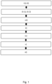
- Figure 1 depicts a flow chart of the process steps of a manufacturing method according to the disclosure for manufacturing a leaded/leadless power/MCD package or power module with less complex and less time-consuming process steps, and wherein the connecting elements being implemented are of a simple design with reduced R DS(on) characteristic.
- the method comprises the steps of i) forming at least one semiconductor package by means of the sub-steps: i1) providing a lead frame made from a metal material having a first frame side and a second frame side opposite to the first frame side as well as having at least two terminals. Subsequently in a step i2) at least one semiconductor die structure is provided having a first die side and a second die side opposite to the first side, which semiconductor die structure is mounted with its second die side on the first frame side of the lead frame.
- connection elements are provided between the at least one semiconductor die structures and the at least two terminals of the lead frame and in a final step ii) the at least one semiconductor die structure, the one or more connection elements and the plurality of terminals are encapsulated with a molding resin leaving at least a portion of at least two terminals exposed, thereby forming at least one encapsulated semiconductor package assembly.
- the step i3) of providing the several electrical and mechanical connection elements comprises at least one forming sequence of the sub steps of i3-1) providing a layer of a metal powder such that the metal powder is in contact with the at least one semiconductor die structure and one of the at least two terminals of the lead frame; and sub-step i3-2) of selectively melting with laser light radiation, the layer of the metal powder to form a metal layer.
- the step of providing a layer of metal powder may constitute depositing the powder particles, whereas the step of selectively melting may also encompass solidifying or sintering the metal powder.
- the connecting elements are formed layer-by-layer through a metal powder layer deposition and solidifying, the known Cu clip bonds or Cu wire bonds are replaced and any process time for panel level packaging is significantly reduced. Furthermore, the manufacturing technique of connecting elements is more flexible compared to the known bond wire / bond clip forming techniques, which requires pre-designed and pre-manufactured components.
- the layer-by-layer deposition technique implemented allows a better material handling, reducing material stresses in the connecting elements thus reducing connectivity failures over time and extending the life span of the resulting leaded/leadless power/MCD package or power module.
- manufacturing technique as outlined in sub-steps i3-1) and i3-2) result in a reduced (lower) R DS(on) characteristic compared to the known conventional interconnect methods. This because the whole interconnecting interface between the various components (semiconductor die structure and lead frame) will be of the same metal layer material. Solder and/or adhesive promoters between the semiconductor die structure and resulting connecting elements and between the connecting elements and the lead frame can be omitted as the metal powder connection can be fused in between the material.
- the forming sequence of the steps i3-1) and i3-2) is performed multiple times alternately, thereby forming a three-dimensional stack of subsequent melted metal layers.
- the method according to the disclosure allows for a more flexible layer-by-layer forming of the connecting elements as a local thickness and/or a local density of each metal layer formed during a forming sequence of the steps i3-1) and i3-2) can be effectively controlled by adjusting one or more manufacturing parameters chosen from the group of:
- each metal layer being formed in step i3-2) in having a thickness of 30-40 ⁇ m, preferably 35 ⁇ m.
- connecting elements in a layer-by-layer fashion allows in an example of the method according to the disclosure to have a surface dimension of a metal layer being larger or smaller than the surface dimension of the metal layer formed during the previous forming sequence.
- complex three-dimensionally shaped connecting elements can be formed depending on their functionality.
- a step iii) is implemented, after a final forming sequence of steps i3-1) and i3-2) but before step ii), which step subjects the exposed portion of the at least two terminals to a surface roughening treatment, for example using a chemical agent.
- the exposed portion of the at least two terminals is plated with a metal plating material.
- a metal plating material for example, electroplating can be used.
- said metal plating material is different from the metal material of the terminals.
- said metal plating material is Tin.
- the method according to the disclosure comprises the step v), performed after step iv), of singulating the encapsulated semiconductor package from the lead frame, thereby forming a single semiconductor package assembly.
- An post-processing step may encompass a visual inspection step vi).
- a step vii) is performed, before the encapsulating step ii) of providing one or more bond wires (e.g. functioning as gate wires) between the semiconductor die structure 2 and one of the other frame terminals.
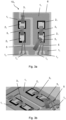
- Figure 2a-2b show a top view and a sectional side view of an example of a singulated leaded semiconductor package assembly 10, according to the disclosure.
- the leaded semiconductor package assembly 10 is formed of three components.
- a first component is a semiconductor die structure 2 with a first die side 2a and a second die side 2b opposite to the first die side 2a.
- a second component is formed as a lead frame 1 made from a metal material has a first frame side 1a and a second frame side 1b opposite to the first frame side 1a and has also at least two leaded terminals 1z 1 .
- the semiconductor die structure 2 is mounted with its second die side 2b on the first frame side 1a of the lead frame 1.
- a three-dimensionally structured connecting element 3 is mounted on the first die side 2a of the semiconductor die structure 2 and is manufactured in accordance with the method steps of the disclosure.
- the three-dimensionally structured connecting element 3 1 bridges the gap or distance between the semiconductor die structure 2 and the leaded terminal 1z, and forms an electrical and mechanical connection.
- each layer deposition in according with sub-step i3-1) is followed by the sub-step i3-2) of selectively melting with laser light radiation L, the layer 30 of the metal powder to form a metal layer 30.
- the step of providing a layer of metal powder may constitute depositing the powder particles, whereas the step of selectively melting may also encompass solidifying or sintering the metal powder.
- the three-dimensionally structured connecting element 3 1 can be regarded as a stack of multiple metal layers 30.
- the forming sequence of the sub steps i3-1) and i3-2) allow a three-dimensional connecting element 3 1 to be structured, here in the shape of a curved bridging element, having a layered first element portion 3 1 -a formed on the semiconductor die structure 2 and a second element portion 3 1 -b formed on the leaded terminal 1z 1 and (the first die side 2a of) the semiconductor die structure 2.
- the specific three-dimensional shape of the connecting element 3 1 can be established in the layer-by-layer forming steps as outlined in the sub-steps i3-1) and i3-2) of the method according to the disclosure.
- the local thickness and/or the local material density (kg/m 3 ) of each metal layer formed during such forming sequence of the sub-steps i3-1) and i3-2) can be effectively controlled by adjusting one or more manufacturing parameters chosen from the group of: a metal powder distribution; a supply velocity of metal powder to be deposited; a metal powder depositing angle relative to a plane formed by the lead frame; a laser light power; a laser light frequency; a laser light wavelength; an ambient process temperature; a metal powder depositing duration time of step i3-1); a metal powder melting duration time of step i3-2).
- metals that can be 3D printed using metal powder, including: stainless steel, titanium, aluminum, cobalt-chrome, inconel, copper, nickel alloys, etc.
- the metal powders used for creating the metal connecting elements 3 are typically created through atomization or gas atomization, and are available in a range of particle sizes and shapes to accommodate the desired circumstances for creating the metal connecting elements 3 during the subs-steps i3-1) and i3-2).
- metal connecting elements 3 can be manufactured having a porous, metal density of e.g. 60%-90%, in particular 75%-85%, more in particular 80% resulting in a more flexible interconnection which has a longer life span and which is less fragile.
- the density of the metal connecting elements 3 can be controlled flexibly at different location and/or in different portions of the elements 3 with the subs-steps i3-1) and i3-2) by adjusting the printing parameter characteristics outlined above.
- metal connecting elements 3 can be formed with an increased electrical conductivity (high density of metal powder) or if desired reduced stress characteristics (lower density of metal powder).
- Figure 3a-3b show a top view and a detailed view of a power module 10 4 according to the disclosure.
- the power module 10 4 is formed of several lead frame parts 1 1 which are electrically separated from each other mounted to a substrate 6.
- Multiple semiconductor die structures 3 1 are mounted to the several lead frame parts 1, and are also electrically attached with each other by means of connection elements 3 1 .
- connection elements 3 are manufactured in a similar fashion as those elements 3 1 of the example of Figure 2a-2b .
- wire bonds 5 are provided between the semiconductor die structures 2, and other terminals 1z 2 of the lead frame 1 1 .
- the whole package of the substrate 6, the semiconductor die structures 2 1 , the connection elements 3 1 , the bond wires 5, the lead frame parts 1 1 , and the plurality of terminals 1z 2 are encapsulated by a molding resin 4 (not shown), with only a portion of the terminals 1z 2 exposed.
- the semiconductor package assembly 10 2 is a singulated leadless semiconductor package assembly. Similar as in the example of Figures 2 and 3 , a semiconductor die structure 2 has a first die side 2a and a second die side 2b opposite to the first die side 2a. A lead frame 1 made from a metal material has a first frame side 1a and a second frame side 1b opposite to the first frame side 1a and has also at least two leadless terminals 1z 2 . The semiconductor die structure 2 is mounted with its second die side 2b on the first frame side 1a of the lead frame 1.
- the three-dimensionally structured connecting element 3 2 is being provided on the first die side 2a of the semiconductor die structure 2 in according with the method steps of the disclosure.
- the three-dimensionally structured connecting element 3 2 is provided in a layer-by-layer fashion by means of the forming sequence of the sub steps of i3-1) providing a layer 30 of a metal powder such that the metal powder is in contact with the at least one semiconductor die structure 2 and one of the at least two leadless terminals 1z 2 of the lead frame 1, followed by the sub-step i3-2) of selectively melting with laser light radiation, the layer 30 of the metal powder to form a metal layer 30.
- the three-dimensionally structured connecting element 3 2 can be regarded as a stack of multiple metal layers 30.
- the forming sequence of the sub steps i3-1) and i3-2) allow a three-dimensional connecting element 3 2 to be structured, formed of a layered first element portion 3 2 -a (the main portion) formed on the semiconductor die structure 2 (and functioning as a heat sink) and a second element portion 3 2 -b functioning as an electrical interconnect between the leadless terminal 1z 2 and (the first die side 2a of) the semiconductor die structure 2.
- wire bonds 5 are provided between the semiconductor die structure 2 and another leadless terminal 1z 2 .
- connection element 3 2 The whole construction of the semiconductor die structure 2, the connection element 3 2 , the bond wires 5 and the plurality of terminals 1z 2 are encapsulated by a molding resin 4, with only a portion of the leadless terminals 1z 2 exposed.
- connecting elements being formed in a layer-by-layer fashion allows metal layers to be formed with a surface dimension 30a (see Figure 4a ), which surface dimension is larger than the surface dimension of the metal layer formed during the previous forming sequence.
- a surface dimension 30a see Figure 4a
- Figure 4a-4b by forming or depositing metal layers 30 on top of previous metal layers with a steadily increasing surface dimensions complex three-dimensionally shaped connecting elements 3 2 can be formed with a funneled shape.
- the connecting element 3 2 exhibits a large layer surface area on top and exposed at the outer surface of the package assembly 10 2 and a smaller layer surface area at the bottom at the interface with the first die side 2a of the semiconductor die structure 2.
- This three-dimensional shape allows the connecting element 3 2 to function as a heat sink.
- FIG. 5a-5b An example with a reverse funneled shape of a connecting element 3 3 is shown in the example of Figures 5a-5b .
- each metal layer 30 being formed with the method sub-steps i3-1) and i3-2) may have a thickness of 30-40 ⁇ m, preferably 35 ⁇ m.
- a local thickness and/or a local material density (kg/m 3 ) of each metal layer formed during such forming sequence of the sub-steps i3-1) and i3-2) can be effectively controlled by adjusting one or more manufacturing parameters chosen from the group of: a metal powder distribution; a supply velocity of metal powder to be deposited; a metal powder depositing angle relative to a plane formed by the lead frame; a laser light power; a laser light frequency; a laser light wavelength; an ambient process temperature; a metal powder depositing duration time of step i3-1); a metal powder melting duration time of step i3-2) and in accordance with the parameter ranges mentioned in connection with the description of the example of Figures 2a-2b . Solder and/or adhesive promoters between the semiconductor die structure and resulting connecting elements and between the connecting elements and the lead frame can be omitted as the metal powder connection can be fused in between the material.
Landscapes
- Chemical & Material Sciences (AREA)
- Engineering & Computer Science (AREA)
- Manufacturing & Machinery (AREA)
- Materials Engineering (AREA)
- Composite Materials (AREA)
- Mechanical Engineering (AREA)
- Structures Or Materials For Encapsulating Or Coating Semiconductor Devices Or Solid State Devices (AREA)
- Physics & Mathematics (AREA)
- Electromagnetism (AREA)
- Optics & Photonics (AREA)
- Lead Frames For Integrated Circuits (AREA)
Abstract
A method for manufacturing a leaded/leadless power/MCD package or power module is proposed with less complex and less time-consuming process steps, and wherein the connecting elements being implemented are of a simple design with reduced RDS(on) characteristic. It comprises the sub-steps i1) providing a lead frame, and providing in step i2) at least one semiconductor die structure on the lead frame. The step i-3) of forming one or more connection elements between the at least one semiconductor die structures and the at least two terminals of the lead frame comprises at least one forming sequence of the sub steps of i3-1) of providing a layer of a metal powder such that the metal powder is in contact with the at least one semiconductor die structure and one of the at least two terminals of the lead frame; and sub-step i3-2) of selectively melting with laser light radiation, the layer of the metal powder to form a metal layer.
In a final step ii) the at least one semiconductor die structure, the one or more connection elements and the plurality of terminals are encapsulated with a molding resin leaving at least a portion of at least two terminals exposed, thereby forming at least one encapsulated semiconductor package assembly.

Description
- The present disclosure relates to techniques for manufacturing a semiconductor package assembly, wherein a semiconductor die structure is mounted to a lead frame having terminals and encapsulated with a molding resin, as well as a semiconductor package assembly obtained with these techniques.
- In conventional leaded/leadless power/MCD packages or power modules various connection elements are implemented for electrically and mechanically interconnecting semiconductor die structures with the various terminals of the lead frame. Examples of such electrical and mechanical connection elements are standard wire bonds, ribbon bonds or clip bonds, which requires different process steps to be applied during the power module or semiconductor package assembly manufacturing process.
- Although these known connection elements are immobilized by means of an encapsulant, these fragile bonds are still prone to connectivity failures over time. In addition, these known bonding techniques are costly, complex, cumbersome and thus time consuming, as they require pre-designed and pre-manufactured connecting elements, and time-consuming handling steps for mounting these connecting elements in the manufacturing process. Also, these conventional leaded/leadless power/MCD packages or power modules still exhibit a high RDS(on) (drain-source on resistance) limiting their performance.
- Accordingly, an object of the present disclosure is to provide a manufacturing technique obviating the above identified problems, resulting in a leaded/leadless power/MCD package or power module manufactured with less complex and less time-consuming process steps, and wherein the connecting elements being implemented are of a straightforward design with reduced RDS(on) characteristic.
- According to a first example of the disclosure, a method for manufacturing a leaded/leadless power/MCD package or power module is proposed with less complex and less time-consuming process steps, and wherein the connecting elements being implemented are of a simple design with reduced RDS(on) characteristic.
- The method comprises the steps of i) forming at least one semiconductor package by means of the sub-steps: i1) providing a lead frame made from a metal material having a first frame side and a second frame side opposite to the first frame side as well as having at least two terminals. Subsequently in a step i2) at least one semiconductor die structure is provided having a first die side and a second die side opposite to the first side, which semiconductor die structure is mounted with its second die side on the first frame side of the lead frame.
- In a subsequent step i-3), one or more connection elements are provided between the at least one semiconductor die structures and the at least two terminals of the lead frame and in a final step ii) the at least one semiconductor die structure, the one or more connection elements and the plurality of terminals are encapsulated with a molding resin leaving at least a portion of at least two terminals exposed, thereby forming at least one encapsulated semiconductor package assembly.
- In particular the step i3) of providing the several connection elements comprises at least one forming sequence of the sub steps of i3-1) providing a layer of a metal powder such that the metal powder is in contact with the at least one semiconductor die structure and one of the at least two terminals of the lead frame; and sub-step i3-2) of selectively melting, with laser light radiation, the layer of the metal powder to form a metal layer.
- With the sequence of the two sub-steps i3-1) and i3-2), wherein the connecting elements are formed layer-by-layer through a metal powder layer deposition and solidifying, the known Cu clip bonds or Cu wire bonds are replaced and any process time for panel level packaging is significantly reduced. Furthermore, the manufacturing technique of connecting elements is more flexible compared to the known bond wire / bond clip forming techniques, which requires pre-designed and pre-manufactured components.
- In addition, the layer-by-layer deposition technique implemented allows a better material handling, reducing material stresses in the connecting elements thus reducing connectivity failures over time and extending the life span of the resulting leaded/leadless power/MCD package or power module. Also, such manufacturing technique as outlined in sub-steps i3-1) and i3-2) result in a reduced (lower) RDS(on) characteristic compared to the known conventional interconnect methods. This because the whole interconnecting interface between the various components (semiconductor die structure and lead frame) will be of the same metal layer material. Solder and/or adhesive promoters between the semiconductor die structure and resulting connecting elements and between the connecting elements and the lead frame can be omitted as the metal powder connection can be fused in between the material.
- In a particular example, the forming sequence of the steps i3-1) and i3-2) is performed multiple times alternately, thereby forming a three-dimensional stack of subsequent melted metal layers.
- Contrary to the known pre-designed and pre-manufactured connecting elements, the method according to the disclosure allows for a more flexible layer-by-layer forming of the connecting elements as a local thickness and/or a local density of each metal layer formed during a forming sequence of the steps i3-1) and i3-2) can be effectively controlled by adjusting one or more manufacturing parameters chosen from the group of:
- a metal powder distribution;
- a supply velocity of metal powder to be deposited;
- a metal powder depositing angle relative to a plane formed by the lead frame;
- a laser light power;
- a laser light frequency;
- a laser light wavelength;
- an ambient process temperature;
- a metal powder depositing duration time of step i3-1);
- a metal powder melting duration time of step i3-2).
- Effectively, the method according to the disclosure allows for each metal layer being formed in step i3-2) in having a thickness of 30-40 µm, preferably 35 µm.
- The above design flexibility of the connecting elements in a layer-by-layer fashion allows in an example of the method according to the disclosure to have a surface dimension of a metal layer being larger or smaller than the surface dimension of the metal layer formed during the previous forming sequence. Herewith complex three-dimensionally shaped connecting elements can be formed depending on their functionality.
- In a further example of the method, a step iii) is implemented, after a final forming sequence of steps i3-1) and i3-2) but before step ii), which step subjects the exposed portion of the at least two terminals to a surface roughening treatment, for example using a chemical agent.
- Accordingly, in a further step iv), after step ii) or step iii), the exposed portion of the at least two terminals is plated with a metal plating material. Preferably, said metal plating material is Tin.
- Finally, the method according to the disclosure comprises the step v), performed after step iv), of singulating the encapsulated semiconductor package from the lead frame, thereby forming a single semiconductor package assembly.
- Likewise the disclosure pertains to a semiconductor package assembly composed of at least one semiconductor die structure electrically and mechanically attached by means of one or more connection elements with at least two terminals and encapsulated by a molding resin such that a portion of the at least two terminals are exposed, wherein the one or more connection elements between the semiconductor die structure and the at least two terminals are formed according to the method steps of the present disclosure.
- In particular examples, the semiconductor package assembly is a leadless semiconductor package assembly or a leaded semiconductor package assembly.
- The disclosure will now be discussed with reference to the drawings, which show in:
-
Figure 1 an example of the process steps of the method according to the disclosure; -
Figure 2a-2b a top view and a sectional side view of an example of a leaded semiconductor package assembly according to the disclosure; -
Figure 3a-3b a top view and a detailed view of an example of a power module according to the disclosure; -
Figure 4a-4b a top view and a sectional side view of an example of a leadless semiconductor package assembly according to the disclosure. - For a proper understanding of the disclosure, in the detailed description below corresponding elements or parts of the disclosure will be denoted with identical reference numerals in the drawings.
- As outlined above, apart from the fragile known electrical and mechanical connection elements being immobilized by means of an encapsulant, they are still prone to connectivity failures over time. In addition, these known bonding techniques are costly, complex, cumbersome and thus time consuming, as they require pre-designed and pre-manufactured connecting elements, and time-consuming handling steps for mounting these connecting elements in the manufacturing process. Also, these conventional leaded/leadless power/MCD packages or power modules still exhibit a high RDS(on) (drain-source on resistance) limiting their performance.
-
Figure 1 depicts a flow chart of the process steps of a manufacturing method according to the disclosure for manufacturing a leaded/leadless power/MCD package or power module with less complex and less time-consuming process steps, and wherein the connecting elements being implemented are of a simple design with reduced RDS(on) characteristic. - The method comprises the steps of i) forming at least one semiconductor package by means of the sub-steps: i1) providing a lead frame made from a metal material having a first frame side and a second frame side opposite to the first frame side as well as having at least two terminals. Subsequently in a step i2) at least one semiconductor die structure is provided having a first die side and a second die side opposite to the first side, which semiconductor die structure is mounted with its second die side on the first frame side of the lead frame.
- In a subsequent step i3), one or more connection elements are provided between the at least one semiconductor die structures and the at least two terminals of the lead frame and in a final step ii) the at least one semiconductor die structure, the one or more connection elements and the plurality of terminals are encapsulated with a molding resin leaving at least a portion of at least two terminals exposed, thereby forming at least one encapsulated semiconductor package assembly.
- In particular the step i3) of providing the several electrical and mechanical connection elements comprises at least one forming sequence of the sub steps of i3-1) providing a layer of a metal powder such that the metal powder is in contact with the at least one semiconductor die structure and one of the at least two terminals of the lead frame; and sub-step i3-2) of selectively melting with laser light radiation, the layer of the metal powder to form a metal layer. The step of providing a layer of metal powder may constitute depositing the powder particles, whereas the step of selectively melting may also encompass solidifying or sintering the metal powder.
- With the sequence of the two sub-steps i3-1) and i3-2), wherein the connecting elements are formed layer-by-layer through a metal powder layer deposition and solidifying, the known Cu clip bonds or Cu wire bonds are replaced and any process time for panel level packaging is significantly reduced. Furthermore, the manufacturing technique of connecting elements is more flexible compared to the known bond wire / bond clip forming techniques, which requires pre-designed and pre-manufactured components.
- In addition, the layer-by-layer deposition technique implemented allows a better material handling, reducing material stresses in the connecting elements thus reducing connectivity failures over time and extending the life span of the resulting leaded/leadless power/MCD package or power module. Also, such manufacturing technique as outlined in sub-steps i3-1) and i3-2) result in a reduced (lower) RDS(on) characteristic compared to the known conventional interconnect methods. This because the whole interconnecting interface between the various components (semiconductor die structure and lead frame) will be of the same metal layer material. Solder and/or adhesive promoters between the semiconductor die structure and resulting connecting elements and between the connecting elements and the lead frame can be omitted as the metal powder connection can be fused in between the material.
- In a particular example, the forming sequence of the steps i3-1) and i3-2) is performed multiple times alternately, thereby forming a three-dimensional stack of subsequent melted metal layers.
- Contrary to the known pre-designed and pre-manufactured connecting elements, the method according to the disclosure allows for a more flexible layer-by-layer forming of the connecting elements as a local thickness and/or a local density of each metal layer formed during a forming sequence of the steps i3-1) and i3-2) can be effectively controlled by adjusting one or more manufacturing parameters chosen from the group of:
- a metal powder distribution;
- a supply velocity of metal powder to be deposited;
- a metal powder depositing angle relative to a plane formed by the lead frame;
- a laser light power;
- a laser light frequency;
- a laser light wavelength;
- an ambient process temperature;
- a metal powder depositing duration time of step i3-1);
- a metal powder melting duration time of step i3-2).
- Effectively, the method according to the disclosure allows for each metal layer being formed in step i3-2) in having a thickness of 30-40 µm, preferably 35 µm.
- The above design flexibility of the connecting elements in a layer-by-layer fashion allows in an example of the method according to the disclosure to have a surface dimension of a metal layer being larger or smaller than the surface dimension of the metal layer formed during the previous forming sequence. Herewith complex three-dimensionally shaped connecting elements can be formed depending on their functionality.
- In a further example of the method, a step iii) is implemented, after a final forming sequence of steps i3-1) and i3-2) but before step ii), which step subjects the exposed portion of the at least two terminals to a surface roughening treatment, for example using a chemical agent.
- Accordingly, in a further step iv), after step ii) or step iii), the exposed portion of the at least two terminals is plated with a metal plating material. For example, electroplating can be used. Preferably, said metal plating material is different from the metal material of the terminals. In an example said metal plating material is Tin.
- Finally, the method according to the disclosure comprises the step v), performed after step iv), of singulating the encapsulated semiconductor package from the lead frame, thereby forming a single semiconductor package assembly.
- An post-processing step may encompass a visual inspection step vi). Optionally, a step vii) is performed, before the encapsulating step ii) of providing one or more bond wires (e.g. functioning as gate wires) between the semiconductor die
structure 2 and one of the other frame terminals. -
Figure 2a-2b show a top view and a sectional side view of an example of a singulated leaded semiconductor package assembly 10, according to the disclosure. The leaded semiconductor package assembly 10, is formed of three components. A first component is asemiconductor die structure 2 with afirst die side 2a and asecond die side 2b opposite to thefirst die side 2a. A second component is formed as alead frame 1 made from a metal material has afirst frame side 1a and asecond frame side 1b opposite to thefirst frame side 1a and has also at least two leaded terminals 1z1. The semiconductor diestructure 2 is mounted with itssecond die side 2b on thefirst frame side 1a of thelead frame 1. - As the third component, a three-dimensionally structured connecting
element 3, is mounted on thefirst die side 2a of the semiconductor diestructure 2 and is manufactured in accordance with the method steps of the disclosure. The three-dimensionally structured connectingelement 31 bridges the gap or distance between the semiconductor diestructure 2 and the leaded terminal 1z, and forms an electrical and mechanical connection. - In particular, it is provided in a layer-by-layer fashion by means of the forming sequence of the sub steps of i3-1) providing a
layer 30 of a metal powder such that the metal powder is in contact with thefirst die side 2a of the semiconductor diestructure 2 and the leaded terminals 1z, of thelead frame 1. Each layer deposition in according with sub-step i3-1) is followed by the sub-step i3-2) of selectively melting with laser light radiation L, thelayer 30 of the metal powder to form ametal layer 30. - It should be note, that the step of providing a layer of metal powder may constitute depositing the powder particles, whereas the step of selectively melting may also encompass solidifying or sintering the metal powder.
- Accordingly, the three-dimensionally structured connecting
element 31 can be regarded as a stack of multiple metal layers 30. The forming sequence of the sub steps i3-1) and i3-2) allow a three-dimensional connectingelement 31 to be structured, here in the shape of a curved bridging element, having a layered first element portion 31-a formed on the semiconductor diestructure 2 and a second element portion 31-b formed on the leaded terminal 1z1 and (thefirst die side 2a of) the semiconductor diestructure 2. - The specific three-dimensional shape of the connecting
element 31 can be established in the layer-by-layer forming steps as outlined in the sub-steps i3-1) and i3-2) of the method according to the disclosure. The local thickness and/or the local material density (kg/m3) of each metal layer formed during such forming sequence of the sub-steps i3-1) and i3-2) can be effectively controlled by adjusting one or more manufacturing parameters chosen from the group of: a metal powder distribution; a supply velocity of metal powder to be deposited; a metal powder depositing angle relative to a plane formed by the lead frame; a laser light power; a laser light frequency; a laser light wavelength; an ambient process temperature; a metal powder depositing duration time of step i3-1); a metal powder melting duration time of step i3-2). - Particular parameter characteristics can be:
- metal powder chosen from the list of metals disclosed below;
- supply velocities;
- a metal powder depositing angle;
- a power distribution of the laser light used;
- laser light frequency;
- laser light wavelength;
- ambient process temperature;
- depositing duration time and melting duration time.
- There are several metals that can be 3D printed using metal powder, including: stainless steel, titanium, aluminum, cobalt-chrome, inconel, copper, nickel alloys, etc. The metal powders used for creating the
metal connecting elements 3 are typically created through atomization or gas atomization, and are available in a range of particle sizes and shapes to accommodate the desired circumstances for creating themetal connecting elements 3 during the subs-steps i3-1) and i3-2). - For example, with the subs-steps i3-1) and i3-2)
metal connecting elements 3 can be manufactured having a porous, metal density of e.g. 60%-90%, in particular 75%-85%, more in particular 80% resulting in a more flexible interconnection which has a longer life span and which is less fragile. - In particular, the density of the
metal connecting elements 3 can be controlled flexibly at different location and/or in different portions of theelements 3 with the subs-steps i3-1) and i3-2) by adjusting the printing parameter characteristics outlined above. Herewithmetal connecting elements 3 can be formed with an increased electrical conductivity (high density of metal powder) or if desired reduced stress characteristics (lower density of metal powder). -
Figure 3a-3b show a top view and a detailed view of a power module 104 according to the disclosure. The power module 104 is formed of severallead frame parts 11 which are electrically separated from each other mounted to asubstrate 6. Multiple semiconductor diestructures 31 are mounted to the severallead frame parts 1, and are also electrically attached with each other by means ofconnection elements 31. Theseconnection elements 3, are manufactured in a similar fashion as thoseelements 31 of the example ofFigure 2a-2b . - Optionally,
wire bonds 5 are provided between the semiconductor diestructures 2, and other terminals 1z2 of thelead frame 11. - The whole package of the
substrate 6, the semiconductor diestructures 21, theconnection elements 31, thebond wires 5, thelead frame parts 11, and the plurality of terminals 1z2 are encapsulated by a molding resin 4 (not shown), with only a portion of the terminals 1z2 exposed. - In another example, depicted in
Figures 4a and 4b , the semiconductor package assembly 102 is a singulated leadless semiconductor package assembly. Similar as in the example ofFigures 2 and3 , asemiconductor die structure 2 has afirst die side 2a and asecond die side 2b opposite to thefirst die side 2a. Alead frame 1 made from a metal material has afirst frame side 1a and asecond frame side 1b opposite to thefirst frame side 1a and has also at least two leadless terminals 1z2. The semiconductor diestructure 2 is mounted with itssecond die side 2b on thefirst frame side 1a of thelead frame 1. - The three-dimensionally structured connecting
element 32 is being provided on thefirst die side 2a of the semiconductor diestructure 2 in according with the method steps of the disclosure. In particular, the three-dimensionally structured connectingelement 32 is provided in a layer-by-layer fashion by means of the forming sequence of the sub steps of i3-1) providing alayer 30 of a metal powder such that the metal powder is in contact with the at least one semiconductor diestructure 2 and one of the at least two leadless terminals 1z2 of thelead frame 1, followed by the sub-step i3-2) of selectively melting with laser light radiation, thelayer 30 of the metal powder to form ametal layer 30. - Accordingly, the three-dimensionally structured connecting
element 32 can be regarded as a stack of multiple metal layers 30. The forming sequence of the sub steps i3-1) and i3-2) allow a three-dimensional connectingelement 32 to be structured, formed of a layered first element portion 32-a (the main portion) formed on the semiconductor die structure 2 (and functioning as a heat sink) and a second element portion 32-b functioning as an electrical interconnect between the leadless terminal 1z2 and (thefirst die side 2a of) the semiconductor diestructure 2. - Optionally,
wire bonds 5 are provided between the semiconductor diestructure 2 and another leadless terminal 1z2. - The whole construction of the semiconductor die
structure 2, theconnection element 32, thebond wires 5 and the plurality of terminals 1z2 are encapsulated by amolding resin 4, with only a portion of the leadless terminals 1z2 exposed. - The above design flexibility of the connecting elements being formed in a layer-by-layer fashion allows metal layers to be formed with a
surface dimension 30a (seeFigure 4a ), which surface dimension is larger than the surface dimension of the metal layer formed during the previous forming sequence. In other words, and as shown inFigure 4a-4b , by forming or depositingmetal layers 30 on top of previous metal layers with a steadily increasing surface dimensions complex three-dimensionally shaped connectingelements 32 can be formed with a funneled shape. In this funneled shape, the connectingelement 32 exhibits a large layer surface area on top and exposed at the outer surface of the package assembly 102 and a smaller layer surface area at the bottom at the interface with thefirst die side 2a of the semiconductor diestructure 2. This three-dimensional shape allows the connectingelement 32 to function as a heat sink. - An example with a reverse funneled shape of a connecting
element 33 is shown in the example ofFigures 5a-5b . - In all examples of the semiconductor package assemblies 101-102-103-104 shown in this disclosure, each
metal layer 30 being formed with the method sub-steps i3-1) and i3-2) may have a thickness of 30-40 µm, preferably 35 µm. Additionally, a local thickness and/or a local material density (kg/m3) of each metal layer formed during such forming sequence of the sub-steps i3-1) and i3-2) can be effectively controlled by adjusting one or more manufacturing parameters chosen from the group of: a metal powder distribution; a supply velocity of metal powder to be deposited; a metal powder depositing angle relative to a plane formed by the lead frame; a laser light power; a laser light frequency; a laser light wavelength; an ambient process temperature; a metal powder depositing duration time of step i3-1); a metal powder melting duration time of step i3-2) and in accordance with the parameter ranges mentioned in connection with the description of the example ofFigures 2a-2b . Solder and/or adhesive promoters between the semiconductor die structure and resulting connecting elements and between the connecting elements and the lead frame can be omitted as the metal powder connection can be fused in between the material. -
- 101-2-3
- semiconductor package (1st, 2nd, 3rd)
- 104
- semiconductor package assembly / power module
- 1
- lead frame
- 1a
- first side of lead frame
- 1b
- second side of lead frame
- 1z,
- leaded terminal
- 1z2
- leadless terminal
- 2-21
- semiconductor die
- 2a
- first die side of semiconductor die
- 2b
- second die side of semiconductor die
- 31-32-33
- electrical/mechanical connection element (1st, 2nd, 3rd example)
- 31-a /32-a
- first element portion
- 31-b /32-b
- second element portion
- 4
- encapsulant
- 5
- additional wire bond element
- 6
- substrate
- 30
- metal powder layer
- 30a
- surface dimension
Claims (12)
- A method for manufacturing a semiconductor package assembly, the method comprising the steps ofi) forming at least one semiconductor package by means of the sub-steps:i1) providing a lead frame made from a metal material having a first frame side and a second frame side opposite to the first frame side as well as having at least two terminals;i2) providing at least one semiconductor die structure having a first die side and a second die side opposite to the first side with its second die side on the first frame side of the lead frame;i3) providing one or more connection elements between the at least one semiconductor die structures and the at least two terminals of the lead frame;andii) encapsulating the at least one semiconductor die structure, the one or more connection elements and the plurality of terminals with a molding resin leaving at least a portion of at least two terminals exposed, thereby forming at least one encapsulated semiconductor package assembly;
wherein the step i3) comprises at least one forming sequence of the sub steps of:i3-1) providing a layer of a metal powder such that the metal powder is in contact with the at least one semiconductor die structure and one of the at least two terminals of the lead frame;i3-2) selectively melting with laser light radiation, the layer of the metal powder to form a metal layer. - The method for manufacturing a semiconductor package assembly according to claim 1, wherein the forming sequence of the steps i3-1) and i3-2) is performed multiple times alternately, thereby forming a three-dimensional stack of subsequent melted metal layers.
- The method for manufacturing a semiconductor package assembly according to claim 1 or 2, further comprising controlling a local thickness and/or a local density of each metal layer formed during a forming sequence of the steps i3-1) and i3-2) by adjusting one or more manufacturing parameters chosen from the group of:- a metal powder distribution;- a supply velocity of metal powder to be deposited;- a metal powder depositing angle relative to a plane formed by the lead frame;- a laser light power;- a laser light frequency;- a laser light wavelength;- an ambient process temperature;- a metal powder depositing duration time of step i3-1);- a metal powder melting duration time of step i3-2).
- The method for manufacturing a semiconductor package assembly according to any one or more of the claims 1-3, wherein each metal layer formed in step i3-2) has a thickness of 30-40 µm, preferably 35 µm.
- The method for manufacturing a semiconductor package assembly according to any one or more of the claims 1-4, wherein a surface dimension of a metal layer is larger than the surface dimension of the metal layer formed during the previous forming sequence.
- The method for manufacturing a semiconductor package assembly according to any one or more of the claims 1-4, wherein a surface dimension of a metal layer is smaller than the surface dimension of the metal layer formed during the previous forming sequence.
- The method for manufacturing a semiconductor package assembly according to any one or more of the claims 1-6, further comprising the step of iii) after a final forming sequence of steps i3-1) and i3-2) but before step ii), subjecting the exposed portion of the at least two terminals to a surface roughening treatment, for example using a chemical agent.
- The method for manufacturing a semiconductor package assembly according to any one or more of the claims 1-7, further comprising the step of iv) after step ii) or step iii), plating the exposed portion of the at least two terminals with a metal plating material.
- The method for manufacturing a semiconductor package assembly according to any one or more of the claims 1-8, further comprising the step v) after step iv), singulating the encapsulated semiconductor package from the lead frame, thereby forming a single semiconductor package assembly.
- A semiconductor package assembly composed of a semiconductor die structure electrically and mechanically attached by means of one or more connection elements with at least two terminals and encapsulated by a molding resin such that a portion of the at least two terminals are exposed, wherein the one or more connection elements between the semiconductor die structure and the at least two terminals are formed according to the method steps of one or more of the method claims 1-9.
- The semiconductor package assembly according to claim 10, wherein the semiconductor package assembly is a leadless semiconductor package assembly.
- The semiconductor package assembly according to claim 10, wherein the semiconductor package assembly is a leaded semiconductor package assembly.
Priority Applications (3)
| Application Number | Priority Date | Filing Date | Title |
|---|---|---|---|
| EP23164967.4A EP4439658A1 (en) | 2023-03-29 | 2023-03-29 | A method for manufacturing a semiconductor package assembly as well as a semiconductor package assembly obtained with this method |
| CN202410349014.8A CN118737839A (en) | 2023-03-29 | 2024-03-26 | Method for manufacturing semiconductor package component and semiconductor package component obtained by using the method |
| US18/620,300 US20240332144A1 (en) | 2023-03-29 | 2024-03-28 | Method for manufacturing a semiconductor package assembly as well as a semiconductor package assembly obtained with this method |
Applications Claiming Priority (1)
| Application Number | Priority Date | Filing Date | Title |
|---|---|---|---|
| EP23164967.4A EP4439658A1 (en) | 2023-03-29 | 2023-03-29 | A method for manufacturing a semiconductor package assembly as well as a semiconductor package assembly obtained with this method |
Publications (1)
| Publication Number | Publication Date |
|---|---|
| EP4439658A1 true EP4439658A1 (en) | 2024-10-02 |
Family
ID=85800472
Family Applications (1)
| Application Number | Title | Priority Date | Filing Date |
|---|---|---|---|
| EP23164967.4A Pending EP4439658A1 (en) | 2023-03-29 | 2023-03-29 | A method for manufacturing a semiconductor package assembly as well as a semiconductor package assembly obtained with this method |
Country Status (3)
| Country | Link |
|---|---|
| US (1) | US20240332144A1 (en) |
| EP (1) | EP4439658A1 (en) |
| CN (1) | CN118737839A (en) |
Families Citing this family (1)
| Publication number | Priority date | Publication date | Assignee | Title |
|---|---|---|---|---|
| CN119458915B (en) * | 2025-01-10 | 2025-04-11 | 芯体素(杭州)科技发展有限公司 | A chip sealing dam preparation method, device, equipment and medium |
Citations (2)
| Publication number | Priority date | Publication date | Assignee | Title |
|---|---|---|---|---|
| US10115645B1 (en) * | 2018-01-09 | 2018-10-30 | Global Circuit Innovations, Inc. | Repackaged reconditioned die method and assembly |
| EP3852132A1 (en) * | 2020-01-20 | 2021-07-21 | Infineon Technologies Austria AG | Additive manufacturing of a frontside or backside interconnect of a semiconductor die |
-
2023
- 2023-03-29 EP EP23164967.4A patent/EP4439658A1/en active Pending
-
2024
- 2024-03-26 CN CN202410349014.8A patent/CN118737839A/en active Pending
- 2024-03-28 US US18/620,300 patent/US20240332144A1/en active Pending
Patent Citations (2)
| Publication number | Priority date | Publication date | Assignee | Title |
|---|---|---|---|---|
| US10115645B1 (en) * | 2018-01-09 | 2018-10-30 | Global Circuit Innovations, Inc. | Repackaged reconditioned die method and assembly |
| EP3852132A1 (en) * | 2020-01-20 | 2021-07-21 | Infineon Technologies Austria AG | Additive manufacturing of a frontside or backside interconnect of a semiconductor die |
Also Published As
| Publication number | Publication date |
|---|---|
| CN118737839A (en) | 2024-10-01 |
| US20240332144A1 (en) | 2024-10-03 |
Similar Documents
| Publication | Publication Date | Title |
|---|---|---|
| JP4042785B2 (en) | Electronic component and manufacturing method thereof | |
| US8749035B2 (en) | Lead carrier with multi-material print formed package components | |
| US8159059B2 (en) | Microelectromechanical device and method for manufacturing the same | |
| EP3533083B1 (en) | Structures and methods for low temperature bonding | |
| JP2014509455A (en) | Semiconductor package with block terminals | |
| WO2017185065A1 (en) | Sintered metal flip chip joints | |
| US6613605B2 (en) | Interconnection method entailing protuberances formed by melting metal over contact areas | |
| EP3840039B1 (en) | A semiconductor device and corresponding method | |
| US20240332144A1 (en) | Method for manufacturing a semiconductor package assembly as well as a semiconductor package assembly obtained with this method | |
| US20030160339A1 (en) | Electronic component and fabrication method thereof | |
| KR20180002812A (en) | A lead carrier structure, and packages formed therefrom without die attach pads | |
| CN108369867A (en) | Capacitor with package thickness control by film and manufacturing method | |
| US12183666B2 (en) | Ceramic laminated substrate, module, and method of manufacturing ceramic laminated substrate | |
| CN114388375A (en) | Method for forming chip package and chip package | |
| CN107134441A (en) | Chip insertion packaging body with welding electrical contacts | |
| US20190096696A1 (en) | Method for filling via hole of ceramic substrate and ceramic substrate via hole filler formed thereby | |
| KR20210090679A (en) | Thermal lensed electrode for thermoelectric generator with improved performance | |
| KR100923784B1 (en) | Metal circuit board with excellent heat dissipation and its manufacturing method | |
| CN1222252A (en) | Method of manufacturing a semiconductor package | |
| JP2009099816A (en) | Semiconductor device, method for manufacturing the same, and method for mounting the semiconductor device | |
| CN107516653A (en) | Small size quad flat non-pin type encapsulates interlayer interconnection structure and manufacture method | |
| JP6736132B1 (en) | Power semiconductor module | |
| JPH01302830A (en) | Electrical circuit device | |
| CN117747588A (en) | Array column structure for chip packaging and preparation method thereof | |
| CN121985835A (en) | Embedded chip packaging substrate and its fabrication method |
Legal Events
| Date | Code | Title | Description |
|---|---|---|---|
| PUAI | Public reference made under article 153(3) epc to a published international application that has entered the european phase |
Free format text: ORIGINAL CODE: 0009012 |
|
| STAA | Information on the status of an ep patent application or granted ep patent |
Free format text: STATUS: THE APPLICATION HAS BEEN PUBLISHED |
|
| AK | Designated contracting states |
Kind code of ref document: A1 Designated state(s): AL AT BE BG CH CY CZ DE DK EE ES FI FR GB GR HR HU IE IS IT LI LT LU LV MC ME MK MT NL NO PL PT RO RS SE SI SK SM TR |
|
| STAA | Information on the status of an ep patent application or granted ep patent |
Free format text: STATUS: REQUEST FOR EXAMINATION WAS MADE |
|
| 17P | Request for examination filed |
Effective date: 20250331 |