EP4439643A1 - Electronic structure, manufacturing method of electronic structure, and manufacturing method of electronic device - Google Patents
Electronic structure, manufacturing method of electronic structure, and manufacturing method of electronic device Download PDFInfo
- Publication number
- EP4439643A1 EP4439643A1 EP24152520.3A EP24152520A EP4439643A1 EP 4439643 A1 EP4439643 A1 EP 4439643A1 EP 24152520 A EP24152520 A EP 24152520A EP 4439643 A1 EP4439643 A1 EP 4439643A1
- Authority
- EP
- European Patent Office
- Prior art keywords
- sacrificial layer
- substrate
- layer
- function part
- holding
- Prior art date
- Legal status (The legal status is an assumption and is not a legal conclusion. Google has not performed a legal analysis and makes no representation as to the accuracy of the status listed.)
- Pending
Links
Images








Classifications
-
- H—ELECTRICITY
- H10—SEMICONDUCTOR DEVICES; ELECTRIC SOLID-STATE DEVICES NOT OTHERWISE PROVIDED FOR
- H10H—INORGANIC LIGHT-EMITTING SEMICONDUCTOR DEVICES HAVING POTENTIAL BARRIERS
- H10H20/00—Individual inorganic light-emitting semiconductor devices having potential barriers, e.g. light-emitting diodes [LED]
- H10H20/80—Constructional details
- H10H20/81—Bodies
- H10H20/819—Bodies characterised by their shape, e.g. curved or truncated substrates
- H10H20/82—Roughened surfaces, e.g. at the interface between epitaxial layers
-
- H—ELECTRICITY
- H10—SEMICONDUCTOR DEVICES; ELECTRIC SOLID-STATE DEVICES NOT OTHERWISE PROVIDED FOR
- H10P—GENERIC PROCESSES OR APPARATUS FOR THE MANUFACTURE OR TREATMENT OF DEVICES COVERED BY CLASS H10
- H10P95/00—Generic processes or apparatus for manufacture or treatments not covered by the other groups of this subclass
- H10P95/11—Separation of active layers from substrates
-
- H—ELECTRICITY
- H10—SEMICONDUCTOR DEVICES; ELECTRIC SOLID-STATE DEVICES NOT OTHERWISE PROVIDED FOR
- H10F—INORGANIC SEMICONDUCTOR DEVICES SENSITIVE TO INFRARED RADIATION, LIGHT, ELECTROMAGNETIC RADIATION OF SHORTER WAVELENGTH OR CORPUSCULAR RADIATION
- H10F71/00—Manufacture or treatment of devices covered by this subclass
- H10F71/139—Manufacture or treatment of devices covered by this subclass using temporary substrates
-
- H—ELECTRICITY
- H10—SEMICONDUCTOR DEVICES; ELECTRIC SOLID-STATE DEVICES NOT OTHERWISE PROVIDED FOR
- H10H—INORGANIC LIGHT-EMITTING SEMICONDUCTOR DEVICES HAVING POTENTIAL BARRIERS
- H10H20/00—Individual inorganic light-emitting semiconductor devices having potential barriers, e.g. light-emitting diodes [LED]
- H10H20/01—Manufacture or treatment
-
- H—ELECTRICITY
- H10—SEMICONDUCTOR DEVICES; ELECTRIC SOLID-STATE DEVICES NOT OTHERWISE PROVIDED FOR
- H10P—GENERIC PROCESSES OR APPARATUS FOR THE MANUFACTURE OR TREATMENT OF DEVICES COVERED BY CLASS H10
- H10P72/00—Handling or holding of wafers, substrates or devices during manufacture or treatment thereof
- H10P72/70—Handling or holding of wafers, substrates or devices during manufacture or treatment thereof for supporting or gripping
- H10P72/74—Handling or holding of wafers, substrates or devices during manufacture or treatment thereof for supporting or gripping using temporarily an auxiliary support
-
- H—ELECTRICITY
- H10—SEMICONDUCTOR DEVICES; ELECTRIC SOLID-STATE DEVICES NOT OTHERWISE PROVIDED FOR
- H10H—INORGANIC LIGHT-EMITTING SEMICONDUCTOR DEVICES HAVING POTENTIAL BARRIERS
- H10H20/00—Individual inorganic light-emitting semiconductor devices having potential barriers, e.g. light-emitting diodes [LED]
- H10H20/01—Manufacture or treatment
- H10H20/011—Manufacture or treatment of bodies, e.g. forming semiconductor layers
- H10H20/018—Bonding of wafers
Definitions
- the present disclosure relates to an electronic structure, a manufacturing method of the electronic structure, and a manufacturing method of an electronic device.
- Patent Reference 1 Japanese Patent Application Publication No. 2009-152387 (see Abstract)
- the support layer is also peeled off from the substrate and transferred onto the transfer substrate together with the function part. Therefore, work of removing the support layer is necessary in the transfer step or a subsequent step. Further, since a part of the support layer is broken at the time of the peeling, there is a possibility that a broken piece adheres to the transfer substrate and causes a defect such as a defective joint. Therefore, it is requested to facilitate the process including the transfer of the function part.
- the object of the present disclosure is to facilitate the process including the transfer of the function part.
- a manufacturing method of an electronic structure in the present disclosure includes a step of forming a second sacrificial layer extending from a substrate to a function part of a layered substrate including the substrate, a first sacrificial layer formed on the substrate, and the function part formed on the first sacrificial layer; a step of forming a cover layer extending from the substrate to the second sacrificial layer; and a step of removing the first sacrificial layer and the second sacrificial layer.
- An electronic structure in the present disclosure includes a substrate, a function part formed on the substrate, and a cover layer formed on the substrate to surround the function part. A gap is formed between the function part and the cover layer.
- a manufacturing method of an electronic device in the present disclosure includes a step of forming a second sacrificial layer extending from a substrate to a function part of a layered substrate including the substrate, a first sacrificial layer formed on the substrate, and the function part formed on the first sacrificial layer; a step of forming a cover layer extending from the substrate to the second sacrificial layer; a step of peeling off the function part from the substrate after removing the first sacrificial layer and the second sacrificial layer; and a step of transferring the function part onto another substrate different from the substrate.
- the first sacrificial layer and the second sacrificial layer are removed and the function part is held on the substrate, and thus the function part can be peeled off from the substrate with ease and transferred onto another substrate. Accordingly, the process including the transfer of the function part can be facilitated.
- the electronic structure is used in a manufacturing process of an electronic device.
- the electronic device is, for example, a photoelectric conversion device or the like including a photoelectric conversion element (light-emitting element, light-receiving element) such as an LED (Light-Emitting Diode).
- a photoelectric conversion element light-emitting element, light-receiving element
- the photoelectric conversion device is used for a photoelectric conversion module such as an LED display or an image sensor.
- the electronic device may also be a piezoelectric device.
- the piezoelectric device is used for, for example, a piezoelectric module such as a piezoelectric sensor, an actuator, an ultrasonic sensor, an ultrasonic generator or a pressure transducer.
- the electronic device may also be a switching element, a power device or the like.
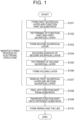
- FIG. 1 is a flowchart showing a manufacturing method of an electronic structure in a first embodiment.
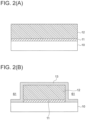
- FIG. 2(A) is a cross-sectional view showing a step of forming a first sacrificial layer 11 and a function part 12 on a substrate 10.
- FIG. 2(B) is a cross-sectional view showing a step of forming a second sacrificial layer 13.
- step S101 ( FIG. 1 ), as shown in FIG. 2(A) , the first sacrificial layer 11 is formed on the substrate 10, and the function part 12 is formed on the first sacrificial layer 11.
- the substrate 10 is a semiconductor substrate or an insulative substrate.
- the substrate 10 is desired to be a GaAs substrate (wafer) suitable for the formation of the semiconductor layer.
- the first sacrificial layer 11 is formed on a surface (upper surface) of the substrate 10.
- the first sacrificial layer 11 is desired to be an AlGaAs layer whose lattice constant is close to that of the function part 12 and whose etching selectivity is high.
- the thickness of the first sacrificial layer 11 is thicker than or equal to 10 nm and thinner than or equal to 1 ⁇ m, for example.
- the function part 12 is a semiconductor layer, for example, and is an epitaxial layer.
- the function part 12 is referred to also as a functional thin film.
- the function part 12 is a heterojunction semiconductor film of GaP/AlInGaP, for example.
- the function part 12 can also be GaAs, InGaP, GaN, AlGaN or InGaN.
- the function part 12 can also be a crystal layer having a piezoelectric property.
- the function part 12 is formed by epitaxial growth on the first sacrificial layer 11 as mentioned earlier. However, it is also possible to epitaxially grow the function part 12 on a substrate different from the substrate 10, peel off the function part 12 from the substrate, and transfer the function part 12 onto the first sacrificial layer 11.
- the first sacrificial layer 11 can be formed of an inorganic film such as Al 2 O 3 , SiO 2 or the like formed by CVD (Chemical Vapor Deposition) or an organic film such as a photoresist or the like.
- the substrate 10 can be a Si substrate, for example.
- a bottom surface of the function part 12, which faces the substrate 10, is a smooth surface whose surface roughness (maximum height Ry) is smaller than or equal to 10 nm.
- step S102 ( FIG. 1 ), as shown in FIG. 2(B) , separation grooves 61 exposing the surface of the substrate 10 are formed by patterning the first sacrificial layer 11 and the function part 12 by means of etching or the like.
- the substrate 10, the first sacrificial layer 11 and the function part 12 are collectively referred to as a layered substrate.
- step S103 the second sacrificial layer 13 extending from the surface of the substrate 10 to the function part 12 is formed.
- the second sacrificial layer 13 is, for example, an inorganic film such as Al 2 O 3 , SiO 2 or the like or an organic film such as a photoresist or the like.
- the thickness of the second sacrificial layer 13 is 100 nm, for example.
- the materials of the first sacrificial layer 11 and the second sacrificial layer 13 are selected so as to be removed by the same etching solution, the first sacrificial layer 11 and the second sacrificial layer 13 can be removed at the same time in step S107 which will be described later.
- the second sacrificial layer 13 is formed from the surface of the substrate 10, which is exposed via the separation grooves 61, and reaches a surface of the function part 12 (i.e., surface of the function part 12 on a side opposite to the substrate 10).
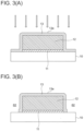
- FIG. 3(A) is a cross-sectional view showing a step of roughening a surface (upper surface) 13e of the second sacrificial layer 13.
- FIG. 3(B) is a cross-sectional view showing a step of patterning the second sacrificial layer 13.
- step S104 ( FIG. 1 ), as shown in FIG. 3(A) , the surface 13e of the second sacrificial layer 13 is roughened.
- the roughening is processing for increasing the surface roughness, and is executed by means of plasma processing such as ashing, for example.
- the roughening is not limited to plasma processing but may also be executed by making particles adhere to the surface 13e of the second sacrificial layer 13.
- the metallic material granularized by self-organization adheres to the surface 13e of the second sacrificial layer 13 and the surface roughness can be increased.
- side faces of the second sacrificial layer 13 are also roughened in addition to the surface 13e of the second sacrificial layer 13.
- the surface roughness of the surface 13e of the second sacrificial layer 13 after the roughening is rougher than the surface roughness of a bottom surface of the function part 12 (i.e., surface of the function part 12 on the substrate 10 side).
- the surface roughness (maximum height Ry) of the surface 13e of the second sacrificial layer 13 is rougher than 10 nm.
- openings 62 are formed by patterning the second sacrificial layer 13.
- the openings 62 are formed in order to facilitate the etching solution to reach the first sacrificial layer 11 in a step of removing the sacrificial layers 11 and 13 (step S107) which will be described later.
- FIGS. 4(A) and 4(B) are a cross-sectional view and a plan view showing a step of forming a holding layer 14.
- FIG. 4(A) corresponds to a cross-sectional view taken along the line 4A - 4A shown in FIG. 4(B) .
- step S106 the holding layer 14 as a cover layer extending from the surface of the substrate 10 to the second sacrificial layer 13 is formed.
- the material of the holding layer 14 is desired to be a material that is not eroded by the etching solution in the step of removing the first sacrificial layer 11 and the second sacrificial layer 13 (step S107) which will be described later.
- an organic resist is used as the material of the holding layer 14.
- a surface 14e of the holding layer 14 in contact with the surface 13e of the second sacrificial layer 13 is roughened similarly to the surface 13e of the second sacrificial layer 13.
- the surface roughness of the surface 14e of the holding layer 14 is rougher than the surface roughness of the bottom surface of the function part 12 (i.e., surface of the function part 12 on the substrate 10 side), for example.
- the surface roughness (maximum height Ry) of the surface 14e of the holding layer 14 is rougher than 10 nm.
- the holding layer 14 includes a top part 14a formed on the surface of the second sacrificial layer 13, a base part 14b formed on the surface of the substrate 10, and a pillar part 14c extending between the top part 14a and the base part 14b.
- the holding layer 14 is desirably patterned as shown in FIG. 4(B) .
- an X direction and a Y direction orthogonal to each other are defined along the surface of the substrate 10.
- a planer shape of the function part 12 is a rectangular shape having two sides extending in the X direction and two sides extending in the Y direction.
- the holding layer 14 includes a first extension part 141 straddling the function part 12 in the X direction and a second extension part 142 straddling the function part 12 in the Y direction.
- the first extension part 141 and the second extension part 142 intersect with each other at the center of the surface of the function part 12.
- openings 63 are formed at positions corresponding to four corners of the function part 12.
- the openings 62 of the second sacrificial layer 13 formed in the above-described step S105 are formed at positions corresponding to the openings 63.
- FIGS. 5(A) and 5(B) are a cross-sectional view and a plan view showing the step of removing the first sacrificial layer 11 and the second sacrificial layer 13.
- FIG. 5(A) corresponds to a cross-sectional view taken along the line 5A - 5A shown in FIG. 5(B) .
- step S107 as shown in FIG. 5(A) , the first sacrificial layer 11 and the second sacrificial layer 13 are removed by means of wet etching.
- etching solution a liquid mixture of phosphoric acid and hydrogen peroxide can be used, for example.
- the function part 12 Due to the removal of the first sacrificial layer 11 and the second sacrificial layer 13, the function part 12 is suspended in the etching solution. In this case, displacement of the function part 12 is inhibited since the function part 12 is surrounded by the holding layer 14.
- the holding layer 14 is provided so as to straddle the function part 12 in the X direction and in the Y direction, the displacement of the function part 12 in a plane parallel to the surface of the substrate 10 is prevented and the position of the function part 12 in a direction orthogonal to the surface of the substrate 10 is also restricted.
- each sacrificial layer it is sufficient that most of the sacrificial layer is removed. That is, it is permissible even if a small part of the sacrificial layer is left unremoved. For example, it is permissible even if a small part of the first sacrificial layer 11 remains on the substrate 10 (see FIG. 10 which will be explained later).
- the function part 12 After the substrate 10 is taken out of the etching solution, the function part 12, due to its own weight, adheres to the surface of the substrate 10 and is held on the surface of the substrate 10.
- the adhesion force between the function part 12 and the surface of the substrate 10 is force due to the wight of the function part 12, and thus is weak adhesion force. Further, a gap A is formed between the function part 12 and the holding layer 14.
- a gap W between a side face of the function part 12 and the holding layer 14 corresponds to the thickness of the second sacrificial layer 13. As the thickness of the second sacrificial layer 13 decreases, the gap W can be decreased and the displacement of the function part 12 while being suspended in the etching solution can be inhibited further. Namely, positional accuracy of the function part 12 on the substrate 10 can be increased.
- the thickness of the second sacrificial layer 13 is 100 nm in this example, the thickness of the second sacrificial layer 13 is not limited to 100 nm.
- the thickness of the second sacrificial layer 13 is desired to be thinner than or equal to 1 ⁇ m since the positional accuracy of the function part 12 on a transfer substrate 20 which will be described later ( FIG. 8(A) ) is required on the order of 1 ⁇ m.
- the materials of the first sacrificial layer 11 and the second sacrificial layer 13 are selected so as to be respectively removed by different etching solutions.
- the function part 12 is held at a position apart from the substrate 10 by the second sacrificial layer 13. Therefore, hanging down of a peripheral part of the function part 12 can be prevented and it is possible to let the etching solution spread over the first sacrificial layer 11. Accordingly, insufficient etching can be eliminated and the first sacrificial layer 11 can be removed efficiently.
- an electronic structure 1 including the substrate 10, the function part 12 and the holding layer 14 and having the gap A between the function part 12 and the holding layer 14 is obtained as shown in FIG. 5(A) .
- the steps S101 to S107 correspond to a manufacturing process of the electronic structure 1.
- FIG. 6(A) is a cross-sectional view showing the electronic structure 1 and a transfer tool 17.
- FIG. 6(B) is a bottom view showing the transfer tool 17.
- step S108 the function part 12 and the holding layer 14 are peeled off from the substrate 10 of the electronic structure 1.
- the transfer tool 17 shown in FIG. 6(A) is used for the peeling.
- the transfer tool 17 includes a holding body 18 and a support substrate 19 that supports the holding body 18.
- the holding body 18, which is desired to have adhesiveness (tackiness) and elasticity, is an organic structure in this example.
- the holding body 18 can be formed of an elastomer or a thick-film resist on a surface of the support substrate 19 formed of a hard material.
- the holding body 18 includes first contact parts 18a that make contact with the surface of the function part 12 and a second contact part 18b that makes contact with a surface of the holding layer 14 (i.e., a surface of the top part 14a).
- the first contact parts 18a are at a position projected toward the electronic structure 1 with respect to the second contact part 18b.
- the first contact parts 18a are arranged in two rows and two columns in the X direction and the Y direction.
- the second contact part 18b is formed as a groove extending in a cross shape like the holding layer 14.
- FIGS. 7(A) and 7(B) are cross-sectional views showing stepwise a step of peeling off the function part 12 and the holding layer 14 from the substrate 10.
- the contact parts 18a and 18b of the holding body 18 of the transfer tool 17 are pressed against the function part 12 and the holding layer 14.
- the holding layer 14 is deformed by being pressed by the holding body 18 from above and makes contact with the surface of the function part 12.
- the adhesion force between the holding layer 14 and the function part 12 is extremely weak since the surface 14e of the holding layer 14 on the function part 12 side has been roughened.
- the transfer tool 17 is moved in a direction away from the substrate 10.
- the function part 12 is peeled off from the substrate 10 together with the holding layer 14 since the adhesion force between the holding body 18 of the transfer tool 17 and the function part 12 is stronger than the adhesion force between the function part 12 and the surface of the substrate 10.
- FIGS. 8(A) and 8(B) are cross-sectional views showing stepwise a step of transferring the function part 12 and the holding layer 14 onto a substrate (referred to as a transfer substrate) different from the substrate 10.
- the transfer substrate 20 has a smooth surface in a mounting region for the function part 12, and the surface roughness (maximum height Ry) of the smooth surface is smaller than or equal to 10 nm.
- the transfer substrate 20 is referred to also as a second substrate.
- step S109 ( FIG. 1 ), as shown in FIG. 8(A) , the transfer tool 17 is moved to a position above the transfer substrate 20, and the function part 12 held by the transfer tool 17 is pressed against the surface of the transfer substrate 20.
- the bottom surface of the function part 12 and the surface of the transfer substrate 20 are both smooth surfaces with surface roughness smaller than or equal to 10 nm. Thus, by performing predetermined pressing and heating, the bottom surface of the function part 12 and the surface of the transfer substrate 20 are joined together by intermolecular force, that is, strong joining force.
- the transfer tool 17 is moved in a direction away from the transfer substrate 20.
- the joining force between the bottom surface of the function part 12 and the surface of the transfer substrate 20 is stronger than the adhesion force between the holding body 18 of the transfer tool 17 and the function part 12 and the holding layer 14. Further, the adhesion force between the holding layer 14 and the function part 12 is extremely weak since the surface 14e of the holding layer 14 on the function part 12 side has been roughened.
- the function part 12 remains being joined to the transfer substrate 20, and the holding layer 14 separates from the transfer substrate 20 together with the transfer tool 17. Since only the function part 12 remains on the transfer substrate 20, it is unnecessary to remove unnecessary members from the surface of the transfer substrate 20.
- FIGS. 9(A) and 9(B) are a cross-sectional view and a plan view showing a step of forming wiring and the like on the function part 12 transferred onto the transfer substrate 20.
- FIG. 9(A) corresponds to a cross-sectional view taken along the line 9A - 9A shown in FIG. 9(B) .
- step S110 ( FIG. 1 ), as shown in FIGS. 9(A) and 9(B) , the wiring and the like are formed on the function part 12.
- the function part 12 is made into an LED, for example, by forming the mesa structure by means of patterning and forming the wiring and the like.
- wiring layers 23 and 24 are formed so as to connect an anode layer 12a and a cathode layer 12b of the function part 12 to wirings 21 and 22 on the transfer substrate 20.
- a semiconductor process it is also possible to use wire bonding or a printing process, for example.
- the electronic device 2 is completed.
- voltage from a drive circuit is applied to the wiring layers 23 and 24 via the wirings 21 and 22, light is emitted from the function part 12 as an LED.
- the electronic structure 1 in this first embodiment is manufactured by forming the first sacrificial layer 11, the function part 12, the second sacrificial layer 13 and the holding layer 14 on the substrate 10 and thereafter removing the first sacrificial layer 11 and the second sacrificial layer 13 as shown in FIG. 5(A) . Accordingly, the function part 12 adheres to the surface of the substrate 10 with weak force and is held on the surface of the substrate 10.
- the function part 12 can be peeled off from the substrate 10 with ease as shown in FIG. 7(B) and transferred onto the transfer substrate 20. Accordingly, the process including the transfer of the function part 12 can be facilitated.
- the holding layer 14 is removed while remaining adhering to the transfer tool 17 as shown in FIG. 8(B) , and thus a step of removing the holding layer 14 from the transfer substrate 20 is unnecessary. Therefore, a printed circuit board, a flexible circuit board or the like on which electronic components and the like have previously been mounted can be used as the transfer substrate 20.
- the holding layer 14 extends from the substrate 10 to the second sacrificial layer 13 as shown in FIG. 4(A) , the displacement of the function part 12 can be inhibited by the holding layer 14 in the step of removing the first sacrificial layer 11 and the second sacrificial layer 13. Therefore, the positional accuracy of the function part 12 on the substrate 10 can be enhanced.
- the surface 14e on the function part 12 side of the holding layer 14 formed on the second sacrificial layer 13 is also roughened.
- the adhesion force between the function part 12 and the holding layer 14 can be weakened and the holding layer 14 can be separated from the function part 12 with ease in the step shown in FIG. 8(B) .
- the manufacturing method of the electronic structure 1 in the first embodiment includes the step of forming the second sacrificial layer 13 extending from the substrate 10 to the function part 12 of the layered substrate including the substrate 10, the first sacrificial layer 11 provided on the substrate 10, and the function part 12 formed on the first sacrificial layer 11; the step of forming the holding layer (cover layer) 14 extending from the substrate 10 to the second sacrificial layer 13; and the step of removing the first sacrificial layer 11 and the second sacrificial layer 13.
- the function part 12 is held in the state of adhering to the substrate 10 with weak adhesion force, and thus the function part 12 can be peeled off from the substrate 10 with ease and transferred onto the transfer substrate 20. Accordingly, the process including the transfer of the function part 12 can be facilitated.
- the holding layer 14 performs the function of inhibiting the displacement of the function part 12. Therefore, the positional accuracy of the function part 12 on the substrate 10 can be increased.
- the holding layer 14 can be separated from the function part 12 with ease after the function part 12 is transferred onto the transfer substrate 20.
- the first sacrificial layer 11 and the second sacrificial layer 13 are removed by using the same etching material, the first sacrificial layer 11 and the second sacrificial layer 13 can be removed by a single step (step S107) and production efficiency can be enhanced further.
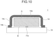
- FIG. 10 is a diagram showing another configuration example of the electronic structure 1. While the electronic structure 1 shown in FIG. 10 is manufactured by a manufacturing method similar to that in the first embodiment, a part (referred to as a remaining part 11a) of the first sacrificial layer 11 is left unremoved in the step S107 ( FIG. 1 ) .
- the substrate 10 and the function part 12 are joined to each other via the remaining part 11a, and thus the effect of inhibiting the displacement of the function part 12 on the substrate 10 is greater. Further, if the area of the remaining part 11a of the first sacrificial layer 11 is set at a minute area, the function part 12 can be peeled off from the substrate 10 with ease in the step S108 ( FIG. 1 ).
- a washing step for removing the remaining part 11a from the bottom surface of the function part 12 is necessary before the transfer step ( FIG. 8(A) ) of transferring the function part 12 onto the transfer substrate 20.
- a function unit 30 including a plurality of elements and wiring layers is used instead of the function part 12 in the first embodiment.
- the function unit 30 is, for example, formed on another growth substrate, peeled off from the growth substrate, and transferred onto the substrate 10.
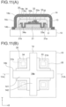
- FIGS. 11(A) and 11(B) are a cross-sectional view and a plan view showing a state in which the first sacrificial layer 11, the function unit 30, the second sacrificial layer 13 and the holding layer 14 have been formed on the substrate 10 in a manufacturing method of an electronic structure 1A in the modification of the first embodiment.
- the function unit 30 as a function part includes a base layer 31, a function layer 32, a first wiring layer 33, a second wiring layer 34, and a capsule layer 35 covering these layers.
- the base layer 31 is formed of an insulator such as SiOz, and is arranged on the first sacrificial layer 11. In the base layer 31, through holes 31a and 31b reaching the first sacrificial layer 11 are formed.
- the bottom surface of the base layer 31 i.e., surface of the base layer 31 on the substrate 10 side
- the function layer 32 is a semiconductor layer, for example, and is an epitaxial layer.
- the function layer 32 includes an anode layer 32a and a cathode layer 32b.
- the function layer 32 is referred to also as a functional thin film.
- the wiring layers 33 and 34 are formed of gold (Au) or alloy of gold, for example.
- the first wiring layer 33 extends from the anode layer 32a of the function layer 32 to the through hole 31a of the base layer 31.
- the first wiring layer 33 is exposed to a bottom surface of the base layer 31 via the through hole 31a and forms an electrode pad 33a.
- the surface roughness of the electrode pad 33a is 10 nm, for example.
- the second wiring layer 34 extends from the cathode layer 32b of the function layer 32 to the through hole 31b of the base layer 31.
- the second wiring layer 34 is exposed to the bottom surface of the base layer 31 via the through hole 31b and forms an electrode pad 34a.
- the surface roughness of the electrode pad 34a is 10 nm, for example.
- the capsule layer 35 is formed of an insulator such as SiOz, and is formed to cover the base layer 31, the function layer 32 and the wiring layers 33 and 34.
- the capsule layer 35 is formed of a material that transmits light.
- An element having a predetermined function is formed by the function layer 32, the first wiring layer 33 and the second wiring layer 34.
- a predetermined function for example, light-emitting function
- FIG. 12(B) which will be explained later, a plurality of elements having different functions are provided in the function unit 30.
- three elements (each including the function layer 32 and the wiring layers 33 and 34) respectively emitting light of red color, green color and blue color are provided in the function unit 30.
- the function unit 30 is provided on the first sacrificial layer 11. Further, the second sacrificial layer 13 is provided on the function unit 30, and the holding layer 14 is provided on the second sacrificial layer 13. Incidentally, the substrate 10, the first sacrificial layer 11 and the function unit 30 are collectively referred to as a layered substrate.
- the first sacrificial layer 11 and the second sacrificial layer 13 are inorganic films or organic films, for example. More specifically, the first sacrificial layer 11 and the second sacrificial layer 13 are formed of a material that is removed by an etching solution not eroding the base layer 31 and the capsule layer 35 of the function unit 30.
- the holding layer 14 is formed of an organic resist, for example.
- the holding layer 14 includes the top part 14a, the base part 14b and the pillar part 14c as described in the first embodiment.
- the surface 13e of the second sacrificial layer 13 is roughened, and the surface 14e of the holding layer 14 in contact with the surface 13e of the second sacrificial layer 13 is also roughened.
- the surface 14e of the holding layer 14 is roughened by roughening the surface 13e of the second sacrificial layer 13 in this example
- the surface 14e of the holding layer 14 may be roughened by a different method. For example, if a surface of the capsule layer 35 of the function unit 30 is roughened, the surface 13e of the second sacrificial layer 13 is roughened accordingly, and the surface 14e of the holding layer 14 can be roughened.
- FIGS. 12(A) and 12(B) are a cross-sectional view and a plan view showing a step of removing the first sacrificial layer 11 and the second sacrificial layer 13.
- FIG. 12(A) corresponds to a cross-sectional view taken along the line 12A - 12A shown in FIG. 12(B) .
- the removal of the first sacrificial layer 11 and the second sacrificial layer 13 is executed by means of wet etching similarly to the step S107 in the first embodiment.
- a material not eroding the base layer 31 and the capsule layer 35 of the function unit 30 is selected.
- the function unit 30 is suspended in the etching solution, displacement of the function unit 30 is inhibited by the holding layer 14.
- the electrode pads 33a and 34a which are parts of the wiring layers 33 and 34, are exposed to the bottom surface of the function unit 30 and make contact with the etching solution.
- the wiring layers 33 and 34 are formed of a material (aforementioned gold or the like) not eroded by the etching solution.
- the function unit 30 adheres to the surface of the substrate 10 with weak adhesion force and is held on the surface of the substrate 10. Further, a gap A is formed between the function unit 30 and the holding layer 14. With these steps, the electronic structure 1A is formed.
- the function unit 30 of the electronic structure 1A is peeled off from the substrate 10 and transferred onto the transfer substrate 20 by the transfer tool 17 by a method similar to the method described with reference to FIG. 6(A) to FIG. 8(B) .
- the function unit 30 adheres to the surface of the substrate 10 with weak adhesion force, the function unit 30 can be peeled off from the substrate 10 with ease.
- the thickness of the second sacrificial layer 13 is desired to be greater than or equal to 1/2 of the width of each electrode pad 33a, 34a in its short-side direction (i.e., widthwise direction).
- the function unit 30 i.e., a complex or composite body
- the function unit 30 including a plurality of elements, wiring and the like can be peeled off from the substrate 10 with ease and transferred onto the transfer substrate 20. Accordingly, the process including the transfer of the function unit 30 can be facilitated.
- the displacement of the function unit 30 is inhibited by the holding layer 14, and thus the positional accuracy of the function unit 30 on the substrate 10 can be increased.
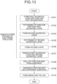
- FIG. 13 is a flowchart showing a manufacturing method of an electronic structure 1B in a second embodiment.
- the second embodiment differs from the first embodiment in that the roughening (the step S104 in FIG. 1 ) is not executed.
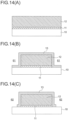
- FIG. 14(A) is a cross-sectional view showing a step of forming the first sacrificial layer 11 and the function part 12 on the substrate 10.
- FIG. 14(B) is a cross-sectional view showing a step of patterning the first sacrificial layer 11 and the function part 12 and forming the second sacrificial layer 13.
- FIG. 14(C) shows a step of patterning the second sacrificial layer 13.
- the first sacrificial layer 11 is formed on the substrate 10, and the function part 12 is formed on the first sacrificial layer 11.
- the separation grooves 61 exposing the surface of the substrate 10 are formed by patterning the first sacrificial layer 11 and the function part 12 by means of etching or the like.
- the substrate 10, the first sacrificial layer 11 and the function part 12 are collectively referred to as a layered substrate.
- the second sacrificial layer 13 extending from the surface of the substrate 10 to the function part 12 is formed.
- the openings 62 are formed by patterning the second sacrificial layer 13.
- FIG. 15(A) is a cross-sectional view showing a step of forming the holding layer 14.
- FIG. 15(B) is a cross-sectional view showing a step of removing the first sacrificial layer 11 and the second sacrificial layer 13.
- step S106 ( FIG. 13 ), as shown in FIG. 15(A) , the holding layer 14 extending from the surface of the substrate 10 to the second sacrificial layer 13 is formed. Since the surface of the second sacrificial layer 13 has not been roughened, the surface of the holding layer 14 in contact with the second sacrificial layer 13 is not roughened either.
- the first sacrificial layer 11 and the second sacrificial layer 13 are removed by means of etching. Due to the removal of the sacrificial layers 11 and 13, the function part 12 adheres to the surface of the substrate 10 with weak adhesion force and is held on the surface of the substrate 10. Further, a gap A is formed between the function part 12 and the holding layer 14. With these steps, the electronic structure 1B is obtained.
- the function part 12 of the electronic structure 1B is peeled off from the substrate 10 and transferred onto the transfer substrate 20 by the transfer tool 17 by a method similar to the method described with reference to FIG. 6(A) to FIG. 8(B) .
- the function part 12 adheres to the surface of the substrate 10 with weak adhesion force as described above, the function part 12 can be peeled off from the substrate 10 with ease in the step of peeling from the substrate 10.
- the surface of the holding layer 14 on the function part 12 side is not roughened.
- the adhesion force between the holding layer 14 and the function part 12 is set to be sufficiently weaker than the joining force between the function part 12 and the surface of the transfer substrate 20 by appropriately selecting the material of the holding layer 14, the holding layer 14 can be peeled off from the transfer substrate 20 while leaving the function part 12 on the transfer substrate 20.
- FIG. 16 is a flowchart showing a manufacturing method of an electronic structure 1C in the third embodiment.
- FIG. 17(A) is a cross-sectional view showing a step of forming a third sacrificial layer 15 and the first sacrificial layer 11 on the substrate 10.
- FIG. 17(B) is a cross-sectional view showing a step of forming the function unit 30 on the first sacrificial layer 11.
- FIG. 17(C) is a cross-sectional view showing a step of forming the second sacrificial layer 13.
- step S201 ( FIG. 16 ), as shown in FIG. 17(A) , the third sacrificial layer 15 is formed on the substrate 10, and the first sacrificial layer 11 is formed on the third sacrificial layer 15.
- the third sacrificial layer 15 is an inorganic film or an organic film, for example.
- the first sacrificial layer 11 is an inorganic film or an organic film, for example. More specifically, the first sacrificial layer 11 is formed of a material that can be removed by an etching solution not eroding the third sacrificial layer 15 and the second sacrificial layer 13 which will be described later.
- step S202 ( FIG. 16 ), as shown in FIG. 17(A) , the separation grooves 61 exposing the surface of the substrate 10 are formed by patterning the third sacrificial layer 15 and the first sacrificial layer 11 by means of dry etching or the like.
- step S203 the function unit 30 is formed on the first sacrificial layer 11.
- the function unit 30 is a complex (composite body) including a plurality of elements and wiring layers.
- the function unit 30 is formed on another growth substrate, peeled off from the growth substrate, and transferred onto the substrate 10.
- the function unit 30 includes the base layer 31, the function layer 32, the first wiring layer 33, the second wiring layer 34, and the capsule layer 35 covering these layers. These layers are the same as those in the modification ( FIG. 11(A) - FIG. 12(B) ) of the first embodiment, and thus repeated description thereof is omitted here.
- the substrate 10, the third sacrificial layer 15, the first sacrificial layer 11 and the function unit 30 are collectively referred to as a layered substrate.
- step S204 the second sacrificial layer 13 extending from the surface of the substrate 10 to the function unit 30 is formed.
- the second sacrificial layer 13 is an inorganic film such as Al 2 O 3 , SiO 2 or the like, for example.
- the thickness of the second sacrificial layer 13 is 100 nm, for example.
- FIG. 18(A) is a cross-sectional view showing a step of roughening the surface of the second sacrificial layer 13.
- FIG. 18(B) is a cross-sectional view showing a step of patterning the second sacrificial layer 13.
- step S205 ( FIG. 16 ), as shown in FIG. 18(A) , the surface 13e of the second sacrificial layer 13 is roughened.
- the method of the roughening it is possible to execute plasma processing such as ashing or to make particles of metal or the like adhere to the surface 13e of the second sacrificial layer 13.
- step S206 ( FIG. 16 ), as shown in FIG. 18(B) , the openings 62 are formed by patterning the second sacrificial layer 13.
- FIG. 19(A) is a cross-sectional view showing a step of forming the holding layer 14.
- FIG. 19(B) is a cross-sectional view showing a step of removing the first sacrificial layer 11.
- step S207 the holding layer 14 as the cover layer extending from the surface of the substrate 10 to the second sacrificial layer 13 is formed.
- the holding layer 14 is formed of a material that is not eroded by the etching solution in a step of removing the first sacrificial layer 11 (step S208) which will be described later, such as an organic resist, for example.
- the surface 14e of the holding layer 14 in contact with the surface 13e of the second sacrificial layer 13 is roughened similarly to the surface 13e of the second sacrificial layer 13.
- the holding layer 14 includes the top part 14a formed on the surface of the second sacrificial layer 13, the base part 14b formed on the surface of the substrate 10, and the pillar part 14c extending between the top part 14a and the base part 14b. Further, the holding layer 14 is desirably patterned in the planer shape shown in FIG. 4(B) in the first embodiment, for example.
- step S208 ( FIG. 16 ), as shown in FIG. 19(B) , the first sacrificial layer 11 is removed by means of wet etching.
- Dilute hydrochloric acid or the like can be used as the etching solution.
- FIGS. 20(A) and 20(B) are a cross-sectional view and a plan view showing a step of roughening a surface of the third sacrificial layer 15.
- FIG. 20(A) corresponds to a cross-sectional view taken along the line 20A - 20A shown in FIG. 20(B) .
- step S209 the surface of the third sacrificial layer 15 is roughened.
- the surface of the third sacrificial layer 15 is situated in the narrow gap C, the roughening by means of plasma processing such as ashing is possible. Further, in cases where the third sacrificial layer 15 is formed of metal, it is also possible to roughen the surface of the third sacrificial layer 15 by means of heating.
- the roughening is executed so that the surface roughness of the third sacrificial layer 15 becomes rougher than that of the bottom surface of the base layer 31 of the function unit 30.
- the roughening is executed so that the surface roughness (maximum height Ry) of the third sacrificial layer 15 becomes rougher than 10 nm.
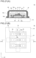
- FIGS. 21(A) and 21(B) are a cross-sectional view and a plan view showing a step of removing the second sacrificial layer 13.
- FIG. 21(A) corresponds to a cross-sectional view taken along the line 21A - 21A shown in FIG. 21(B) .
- the holding layer 14 is indicated by broken lines.
- step S210 the second sacrificial layer 13 is removed by means of wet etching.
- Phosphoric acid or the like can be used as the etching solution.
- the function unit 30 is, due to its own weight, held on the surface of the third sacrificial layer 15. Since the surface of the third sacrificial layer 15 has been roughened, the adhesion force between the third sacrificial layer 15 and the function unit 30 is extremely weak. Further, a gap A is formed between the function unit 30 and the holding layer 14.
- the electronic structure 1C including the substrate 10, the function unit 30 and the holding layer 14 and having the gap A between the function unit 30 and the holding layer 14 is obtained as shown in FIG. 21(B) .
- the steps S201 to S210 correspond to the manufacturing process of the electronic structure 1C.
- FIGS. 22(A) and 22(B) are cross-sectional views showing stepwise a step of peeling off the function unit 30 and the holding layer 14 from the substrate 10.
- step S211 the function unit 30 and the holding layer 14 are peeled off from the substrate 10 of the electronic structure 1C.
- the transfer tool 17 shown in FIG. 22(A) is used for the peeling.
- the configuration of the transfer tool 17 is as described in the first embodiment.
- the holding body 18 of the transfer tool 17 is pressed against the function unit 30 and the holding layer 14.
- the holding layer 14 is deformed by being pressed by the holding body 18 from above and makes contact with the surface of the function unit 30.
- the adhesion force between the holding layer 14 and the function unit 30 is extremely weak since the surface 14e of the holding layer 14 on the function unit 30 side has been roughened.
- the transfer tool 17 is moved in the direction away from the substrate 10.
- the adhesion force between the holding body 18 of the transfer tool 17 and the function unit 30 is stronger than the adhesion force between the function unit 30 and the third sacrificial layer 15. Therefore, the function unit 30 is peeled off from the substrate 10 together with the holding layer 14.
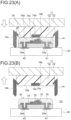
- FIGS. 23(A) and 23(B) are cross-sectional views showing stepwise a step of transferring the function unit 30 onto a transfer substrate 40 different from the substrate 10. While the transfer substrate 40 is configured similarly to the transfer substrate 20 described in the first embodiment, wirings 41 and 42 have previously been formed on the transfer substrate 40.
- step S212 ( FIG. 16 ), as shown in FIG. 23 (A) , the transfer tool 17 is moved to a position above the transfer substrate 40, and the function unit 30 held by the transfer tool 17 is pressed against the transfer substrate 40.
- the bottom surface of the function unit 30 and the surface of the transfer substrate 40 are smooth surfaces with surface roughness (maximum height Ry) smaller than or equal to 10 nm.
- surface roughness maximum height Ry
- the bottom surface of the function unit 30 and the surface (i.e., top surface) of the transfer substrate 40 are joined together by intermolecular force, that is, strong joining force.
- the function unit 30 is transferred onto the transfer substrate 40 so that three elements (each including the function layer 32 and the wiring layers 33 and 34) are arranged in the Y direction.
- step S210 the displacement of the function unit 30 is inhibited by the holding layer 14, by which misalignment of the electrode pads 33a and 34a of the function unit 30 and the wirings 41 and 42 of the transfer substrate 40 can be reduced to a minimum.
- the joining force between the bottom surface of the function unit 30 and the surface of the transfer substrate 40 is stronger than the adhesion force between the holding body 18 of the transfer tool 17 and the function unit 30 and the holding layer 14. Further, the adhesion force between the holding layer 14 and the function unit 30 is weak since the surface 14e of the holding layer 14 on the function unit 30 side has been roughened.
- the function unit 30 remains being joined to the transfer substrate 40, and the holding layer 14 separates from the transfer substrate 40 together with the transfer tool 17.
- the electronic device 2C in which the function unit 30 is arranged on the transfer substrate 40 is obtained.
- voltage from a non-illustrated drive circuit is applied to the wiring layers 33 and 34 via the wirings 41 and 42, light of the red color, the green color and the blue color is respectively emitted from the three elements of the function unit 30.
- the surface of the third sacrificial layer 15 on the substrate 10 is roughened after removing the first sacrificial layer 11.
- the function unit 30 is held on the roughened surface of the third sacrificial layer 15, and thus the adhesion force between the function unit 30 and the third sacrificial layer 15 is weak. Therefore, in the peeling step, the function unit 30 can be peeled off from the third sacrificial layer 15 with ease.
- FIGS. 24 (A) and 24 (B) are a cross-sectional view and a plan view showing a state in which the first sacrificial layer 11, the function unit 30, the second sacrificial layer 13 and holding layers 51 are formed on the substrate 10 in a manufacturing method of an electronic structure 1D in the fourth embodiment.
- a plurality of holding layers 51 as cover layers arranged along an outer periphery of the function unit 30 are used instead of the holding layer 14 in the first embodiment.
- four holding layers 51 are respectively arranged at four sides of the function unit 30 as shown in FIG. 24(B) .
- holding layers 51 are respectively arranged at positions for sandwiching the function unit 30 from both sides in the X direction and from both sides in the Y direction.
- the positions of the holding layers 51 are not limited to the four sides of the function unit 30.
- the holding layers 51 may be arranged at four corners of the function unit 30, for example.
- Each holding layer 51 is formed of an organic resist, for example.
- the holding layers 51 do not reach a central region of the function unit 30 in a top view.
- the holding body 18 of the transfer tool 17 can be brought into contact with the function unit 30 alone, without having the holding body 18 make contact with the holding layers 51.
- each holding layer 51 includes a top part 51a situated on the surface of the second sacrificial layer 13, a base part 51b formed on the substrate 10, and a pillar part 51c extending between the top part 51a and the base part 51b.
- a corner part 51d between the top part 51a and the pillar part 51c follows a curved shape of a corner part 30a of the capsule layer 35 of the function unit 30, and is formed in a similar curved shape.
- a minimum distance Dx between the top parts 51a of two holding layers 51 facing each other in the X direction is shorter than the width of the function unit 30 in the X direction.
- a minimum distance Dy between the top parts 51a of holding layers 51 facing each other in the Y direction is shorter than the width of the function unit 30 in the Y direction.
- FIGS. 25(A) and 25(B) are a cross-sectional view and a plan view showing a step of removing the first sacrificial layer 11 and the second sacrificial layer 13 by means of wet etching.
- FIG. 25(A) corresponds to a cross-sectional view taken along the line 25A - 25A shown in FIG. 25 (B) .
- the function unit 30 is suspended in the etching solution.
- the function unit 30 is surrounded by the plurality of holding layers 51 as shown in FIG. 25(A) , the displacement of the function unit 30 in a plane parallel to the surface of the substrate 10 is inhibited and displacement of the function unit 30 in the direction orthogonal to the surface of the substrate 10 is also restricted.
- the function unit 30 Due to the removal of the first sacrificial layer 11 and the second sacrificial layer 13, the function unit 30 is held in the state of adhering to the surface of the substrate 10 with weak adhesion force. Further, a gap A is formed between the function unit 30 and each holding layer 51. With these steps, the electronic structure 1D is obtained.
- FIGS. 26(A) and 26(B) are cross-sectional views showing stepwise a step of peeling off the function unit 30 of the electronic structure 1D from the substrate 10.
- the transfer tool 17 described in the first embodiment is used for the peeling of the function unit 30.
- the holding body 18 of the transfer tool 17 is pressed against the upper surface of the function unit 30. Since the top parts 51a of the holding layers 51 do not reach the central region of the function unit 30, the holding body 18 can be brought into contact with the function unit 30 alone, without having the holding body 18 make contact with the holding layers 51.
- the holding layers 51 are formed of an organic resist and have elasticity and flexibility to some extent, and thus are capable of elastic deformation when they are pushed by the function unit 30. Therefore, the function unit 30 can be separated from the substrate 10 without breaking the holding layers 51.
- the transfer of the function unit 30 onto the transfer substrate 40 is as described with reference to FIGS. 23(A) and 23(B) in the third embodiment. However, since the holding layers 51 do not adhere to the transfer tool 17, the function unit 30 can be transferred onto the transfer substrate 40 with ease.
- the transfer tool 17 can be reused since the holding layers 51 do not remain on the transfer tool 17.
- the number of holding layers 51 is not limited to four and it is sufficient that the number is two or more.
- the function part 12 in the first embodiment may be used instead of the function unit 30.
- the third sacrificial layer 15 described in the third embodiment may be provided.
- the substrate 10, the third sacrificial layer 15, the first sacrificial layer 11 and the function unit 30 (or the function part 12) are collectively referred to as a layered substrate.
- the fourth embodiment since a plurality of holding layers (cover layers) 51 arranged to be separate from each other are used, the displacement of the function unit 30 at the time of removing the sacrificial layers 11 and 13 can be prevented and the transfer tool 17 can be brought into contact with the function unit 30 alone. Thus, the process including the transfer can be facilitated. Further, the holding layers 51 do not remain on the transfer tool 17 and thus it is possible to reuse the transfer tool 17.
- the present disclosure is applicable to manufacturing methods of electronic devices such as piezoelectric devices, photoelectric conversion devices, switching elements and power devices.
- a manufacturing method of an electronic device comprising:
- 1, 1A, 1B, 1C, 1D electronic structure
- 2, 2C electronic device
- 10 substrate (first substrate), 11: first sacrificial layer, 12: function part, 13: second sacrificial layer, 13e: surface
- 14 holding layer (cover layer), 14e: surface
- 15 third sacrificial layer (sacrificial layer, third sacrificial layer)
- 17 transfer tool
- 18 holding body
- 19 support substrate
- 20, 40 transfer substrate (second substrate)
- 33 first wiring layer
- 33a, 34a electrode pad
- 34 second wiring layer
- 35 capsule layer (cover layer)
Landscapes
- Micromachines (AREA)
- Manufacturing Of Printed Wiring (AREA)
- Apparatuses And Processes For Manufacturing Resistors (AREA)
- Formation Of Insulating Films (AREA)
- Pressure Sensors (AREA)
- Piezo-Electric Or Mechanical Vibrators, Or Delay Or Filter Circuits (AREA)
- Led Device Packages (AREA)
Abstract
A manufacturing method of an electronic structure (1) includes a step of forming a second sacrificial layer (13) extending from a substrate (10) to a function part (12) of a layered substrate including the substrate (10), a first sacrificial layer (11) formed on the substrate (10), and the function part (12) formed on the first sacrificial layer (11). The manufacturing method includes a step of forming a cover layer (14) extending from the substrate (10) to the second sacrificial layer (13), and a step of removing the first sacrificial layer (11) and the second sacrificial layer (13).
Description
- The present disclosure relates to an electronic structure, a manufacturing method of the electronic structure, and a manufacturing method of an electronic device.
- There has been known a technology of forming a function part on a substrate via a support layer, peeling off the function part from the substrate, and transferring the function part onto another substrate (referred to also as a transfer substrate) (see
Patent Reference 1, for example). - Patent Reference 1:
Japanese Patent Application Publication No. 2009-152387 - In the aforementioned conventional technology, the support layer is also peeled off from the substrate and transferred onto the transfer substrate together with the function part. Therefore, work of removing the support layer is necessary in the transfer step or a subsequent step. Further, since a part of the support layer is broken at the time of the peeling, there is a possibility that a broken piece adheres to the transfer substrate and causes a defect such as a defective joint. Therefore, it is requested to facilitate the process including the transfer of the function part.
- The object of the present disclosure is to facilitate the process including the transfer of the function part.
- A manufacturing method of an electronic structure in the present disclosure includes a step of forming a second sacrificial layer extending from a substrate to a function part of a layered substrate including the substrate, a first sacrificial layer formed on the substrate, and the function part formed on the first sacrificial layer; a step of forming a cover layer extending from the substrate to the second sacrificial layer; and a step of removing the first sacrificial layer and the second sacrificial layer.
- An electronic structure in the present disclosure includes a substrate, a function part formed on the substrate, and a cover layer formed on the substrate to surround the function part. A gap is formed between the function part and the cover layer.
- A manufacturing method of an electronic device in the present disclosure includes a step of forming a second sacrificial layer extending from a substrate to a function part of a layered substrate including the substrate, a first sacrificial layer formed on the substrate, and the function part formed on the first sacrificial layer; a step of forming a cover layer extending from the substrate to the second sacrificial layer; a step of peeling off the function part from the substrate after removing the first sacrificial layer and the second sacrificial layer; and a step of transferring the function part onto another substrate different from the substrate.
- According to the present disclosure, the first sacrificial layer and the second sacrificial layer are removed and the function part is held on the substrate, and thus the function part can be peeled off from the substrate with ease and transferred onto another substrate. Accordingly, the process including the transfer of the function part can be facilitated.
-
-
FIG. 1 is a flowchart showing a manufacturing method of an electronic structure in a first embodiment. -
FIG. 2(A) is a cross-sectional view showing a step of forming a first sacrificial layer and a function part on a substrate in the manufacturing method of the electronic structure in the first embodiment. -
FIG. 2(B) is a cross-sectional view showing a step of forming a second sacrificial layer in the manufacturing method of the electronic structure in the first embodiment. -
FIG. 3(A) is a cross-sectional view showing a step of roughening a surface of the second sacrificial layer in the manufacturing method of the electronic structure in the first embodiment. -
FIG. 3(B) is a cross-sectional view showing a step of patterning the second sacrificial layer in the manufacturing method of the electronic structure in the first embodiment. -
FIGS. 4(A) and 4(B) are a cross-sectional view and a plan view showing a step of forming a holding layer (cover layer) in the manufacturing method of the electronic structure in the first embodiment. -
FIGS. 5(A) and 5(B) are a cross-sectional view and a bottom view showing a step of removing the first sacrificial layer and the second sacrificial layer in the manufacturing method of the electronic structure in the first embodiment. -
FIGS. 6(A) and 6(B) are a cross-sectional view and a plan view showing the electronic structure and a transfer tool in the first embodiment. -
FIGS. 7(A) and 7(B) are cross-sectional views showing stepwise a step of peeling off the function part of the electronic structure from the substrate in the first embodiment. -
FIGS. 8(A) and 8(B) are cross-sectional views showing stepwise a step of transferring the function part of the electronic structure onto a transfer substrate in the first embodiment -
FIGS. 9(A) and 9(B) are a cross-sectional view and a plan view showing a step of forming wiring and the like on the function part transferred from the electronic structure onto the transfer substrate in the first embodiment. -
FIG. 10 is a cross-sectional view showing another configuration example of the electronic structure in the first embodiment. -
FIGS. 11(A) and 11(B) are a cross-sectional view and a plan view showing a state in which the first sacrificial layer, a function unit, the second sacrificial layer and the holding layer are formed on the substrate in a manufacturing method of an electronic structure in a modification. -
FIGS. 12(A) and 12(B) are a cross-sectional view and a plan view showing a step of removing the first sacrificial layer and the second sacrificial layer in the manufacturing method of the electronic structure in the modification. -
FIG. 13 is a flowchart showing a manufacturing method of an electronic structure in a second embodiment. -
FIG. 14 (A) is a cross-sectional view showing a step of forming a first sacrificial layer and a function part on a substrate in the manufacturing method of the electronic structure in the second embodiment. -
FIG. 14(B) is a cross-sectional view showing a step of forming a second sacrificial layer in the manufacturing method of the electronic structure in the second embodiment. -
FIG. 14(C) is a cross-sectional view showing a step of patterning the second sacrificial layer in the manufacturing method of the electronic structure in the second embodiment. -
FIG. 15(A) is a cross-sectional view showing a step of forming a holding layer in the manufacturing method of the electronic structure in the second embodiment. -
FIG. 15(B) is a cross-sectional view showing a step of removing the first sacrificial layer and the second sacrificial layer in the manufacturing method of the electronic structure in the second embodiment. -
FIG. 16 is a flowchart showing a manufacturing method of an electronic structure in a third embodiment. -
FIG. 17(A) is a cross-sectional view showing a step of forming a third sacrificial layer and a first sacrificial layer on a substrate in the manufacturing method of the electronic structure in the third embodiment. -
FIG. 17(B) is a cross-sectional view showing a step of forming a function unit on the first sacrificial layer in the manufacturing method of the electronic structure in the third embodiment. -
FIG. 17(C) is a cross-sectional view showing a step of forming a second sacrificial layer in the manufacturing method of the electronic structure in the third embodiment. -
FIG. 18(A) is a cross-sectional view showing a step of roughening a surface of the second sacrificial layer in the manufacturing method of the electronic structure in the third embodiment. -
FIG. 18(B) is a cross-sectional view showing a step of patterning the second sacrificial layer in the manufacturing method of the electronic structure in the third embodiment. -
FIG. 19(A) is a cross-sectional view showing a step of forming a holding layer in the manufacturing method of the electronic structure in the third embodiment. -
FIG. 19(B) is a cross-sectional view showing a step of removing the first sacrificial layer in the manufacturing method of the electronic structure in the third embodiment. -
FIGS. 20(A) and 20(B) are a cross-sectional view and a plan view showing a step of roughening a surface of the third sacrificial layer in the manufacturing method of the electronic structure in the third embodiment. -
FIGS. 21(A) and 21(B) are a cross-sectional view and a plan view showing a step of removing the second sacrificial layer in the manufacturing method of the electronic structure in the third embodiment. -
FIGS. 22(A) and 22(B) are cross-sectional views showing stepwise a step of peeling off the function unit of the electronic structure from the substrate in the third embodiment. -
FIGS. 23(A) and 23(B) are cross-sectional views showing stepwise a step of transferring the function unit of the electronic structure onto a transfer substrate in the third embodiment. -
FIGS. 24(A) and 24(B) are a cross-sectional view and a plan view showing a state in which a first sacrificial layer, a function unit, a second sacrificial layer and holding layers are formed on a substrate in a manufacturing method of an electronic structure in a fourth embodiment. -
FIGS. 25(A) and 25(B) are a cross-sectional view and a plan view showing the electronic structure in the fourth embodiment. -
FIGS. 26(A) and 26(B) are cross-sectional views showing stepwise a step of peeling off the function part of the electronic structure from the substrate in the fourth embodiment. - An electronic structure and its manufacturing method according to each embodiment will be described below with reference to the drawings. The electronic structure is used in a manufacturing process of an electronic device.
- The electronic device is, for example, a photoelectric conversion device or the like including a photoelectric conversion element (light-emitting element, light-receiving element) such as an LED (Light-Emitting Diode). The photoelectric conversion device is used for a photoelectric conversion module such as an LED display or an image sensor.
- Further, the electronic device may also be a piezoelectric device. The piezoelectric device is used for, for example, a piezoelectric module such as a piezoelectric sensor, an actuator, an ultrasonic sensor, an ultrasonic generator or a pressure transducer. Furthermore, the electronic device may also be a switching element, a power device or the like.
-
FIG. 1 is a flowchart showing a manufacturing method of an electronic structure in a first embodiment.FIG. 2(A) is a cross-sectional view showing a step of forming a firstsacrificial layer 11 and afunction part 12 on asubstrate 10.FIG. 2(B) is a cross-sectional view showing a step of forming a secondsacrificial layer 13. - In step S101 (
FIG. 1 ), as shown inFIG. 2(A) , the firstsacrificial layer 11 is formed on thesubstrate 10, and thefunction part 12 is formed on the firstsacrificial layer 11. - The
substrate 10 is a semiconductor substrate or an insulative substrate. In cases where thefunction part 12 which will be described below is a semiconductor layer to be formed into a light-emitting element, thesubstrate 10 is desired to be a GaAs substrate (wafer) suitable for the formation of the semiconductor layer. - The first
sacrificial layer 11 is formed on a surface (upper surface) of thesubstrate 10. In cases where thefunction part 12 is grown epitaxially on the firstsacrificial layer 11, the firstsacrificial layer 11 is desired to be an AlGaAs layer whose lattice constant is close to that of thefunction part 12 and whose etching selectivity is high. The thickness of the firstsacrificial layer 11 is thicker than or equal to 10 nm and thinner than or equal to 1 µm, for example. - The
function part 12 is a semiconductor layer, for example, and is an epitaxial layer. Thefunction part 12 is referred to also as a functional thin film. - The
function part 12 is a heterojunction semiconductor film of GaP/AlInGaP, for example. Thefunction part 12 can also be GaAs, InGaP, GaN, AlGaN or InGaN. Thefunction part 12 can also be a crystal layer having a piezoelectric property. - The
function part 12 is formed by epitaxial growth on the firstsacrificial layer 11 as mentioned earlier. However, it is also possible to epitaxially grow thefunction part 12 on a substrate different from thesubstrate 10, peel off thefunction part 12 from the substrate, and transfer thefunction part 12 onto the firstsacrificial layer 11. In this case, the firstsacrificial layer 11 can be formed of an inorganic film such as Al2O3, SiO2 or the like formed by CVD (Chemical Vapor Deposition) or an organic film such as a photoresist or the like. Thesubstrate 10 can be a Si substrate, for example. - A bottom surface of the
function part 12, which faces thesubstrate 10, is a smooth surface whose surface roughness (maximum height Ry) is smaller than or equal to 10 nm. - In step S102 (
FIG. 1 ), as shown inFIG. 2(B) ,separation grooves 61 exposing the surface of thesubstrate 10 are formed by patterning the firstsacrificial layer 11 and thefunction part 12 by means of etching or the like. Incidentally, thesubstrate 10, the firstsacrificial layer 11 and thefunction part 12 are collectively referred to as a layered substrate. - In step S103 (
FIG. 1 ), as shown inFIG. 2(B) , the secondsacrificial layer 13 extending from the surface of thesubstrate 10 to thefunction part 12 is formed. The secondsacrificial layer 13 is, for example, an inorganic film such as Al2O3, SiO2 or the like or an organic film such as a photoresist or the like. The thickness of the secondsacrificial layer 13 is 100 nm, for example. - If the materials of the first
sacrificial layer 11 and the secondsacrificial layer 13 are selected so as to be removed by the same etching solution, the firstsacrificial layer 11 and the secondsacrificial layer 13 can be removed at the same time in step S107 which will be described later. - The second
sacrificial layer 13 is formed from the surface of thesubstrate 10, which is exposed via theseparation grooves 61, and reaches a surface of the function part 12 (i.e., surface of thefunction part 12 on a side opposite to the substrate 10). -
FIG. 3(A) is a cross-sectional view showing a step of roughening a surface (upper surface) 13e of the secondsacrificial layer 13.FIG. 3(B) is a cross-sectional view showing a step of patterning the secondsacrificial layer 13. - In step S104 (
FIG. 1 ), as shown inFIG. 3(A) , thesurface 13e of the secondsacrificial layer 13 is roughened. The roughening is processing for increasing the surface roughness, and is executed by means of plasma processing such as ashing, for example. - The roughening is not limited to plasma processing but may also be executed by making particles adhere to the
surface 13e of the secondsacrificial layer 13. For example, by means of vacuum evaporation of a metallic material, the metallic material granularized by self-organization adheres to thesurface 13e of the secondsacrificial layer 13 and the surface roughness can be increased. Irrespective of which roughening method is used, side faces of the secondsacrificial layer 13 are also roughened in addition to thesurface 13e of the secondsacrificial layer 13. - The surface roughness of the
surface 13e of the secondsacrificial layer 13 after the roughening is rougher than the surface roughness of a bottom surface of the function part 12 (i.e., surface of thefunction part 12 on thesubstrate 10 side). As an example, the surface roughness (maximum height Ry) of thesurface 13e of the secondsacrificial layer 13 is rougher than 10 nm. - In step S105 (
FIG. 1 ), as shown inFIG. 3(B) ,openings 62 are formed by patterning the secondsacrificial layer 13. Theopenings 62 are formed in order to facilitate the etching solution to reach the firstsacrificial layer 11 in a step of removing thesacrificial layers 11 and 13 (step S107) which will be described later. -
FIGS. 4(A) and 4(B) are a cross-sectional view and a plan view showing a step of forming aholding layer 14. Incidentally,FIG. 4(A) corresponds to a cross-sectional view taken along theline 4A - 4A shown inFIG. 4(B) . - In step S106 (
FIG. 1 ), as shown inFIG. 4(A) , the holdinglayer 14 as a cover layer extending from the surface of thesubstrate 10 to the secondsacrificial layer 13 is formed. The material of the holdinglayer 14 is desired to be a material that is not eroded by the etching solution in the step of removing the firstsacrificial layer 11 and the second sacrificial layer 13 (step S107) which will be described later. As an example, an organic resist is used as the material of the holdinglayer 14. - A
surface 14e of the holdinglayer 14 in contact with thesurface 13e of the secondsacrificial layer 13 is roughened similarly to thesurface 13e of the secondsacrificial layer 13. The surface roughness of thesurface 14e of the holdinglayer 14 is rougher than the surface roughness of the bottom surface of the function part 12 (i.e., surface of thefunction part 12 on thesubstrate 10 side), for example. As an example, the surface roughness (maximum height Ry) of thesurface 14e of the holdinglayer 14 is rougher than 10 nm. - As shown in
FIG. 4(A) , the holdinglayer 14 includes atop part 14a formed on the surface of the secondsacrificial layer 13, abase part 14b formed on the surface of thesubstrate 10, and apillar part 14c extending between thetop part 14a and thebase part 14b. - Further, the holding
layer 14 is desirably patterned as shown inFIG. 4(B) . Here, along the surface of thesubstrate 10, an X direction and a Y direction orthogonal to each other are defined. A planer shape of thefunction part 12 is a rectangular shape having two sides extending in the X direction and two sides extending in the Y direction. - In a top view, the holding
layer 14 includes afirst extension part 141 straddling thefunction part 12 in the X direction and asecond extension part 142 straddling thefunction part 12 in the Y direction. Thefirst extension part 141 and thesecond extension part 142 intersect with each other at the center of the surface of thefunction part 12. - Since the holding
layer 14 is patterned as above,openings 63 are formed at positions corresponding to four corners of thefunction part 12. Incidentally, theopenings 62 of the secondsacrificial layer 13 formed in the above-described step S105 are formed at positions corresponding to theopenings 63. -
FIGS. 5(A) and 5(B) are a cross-sectional view and a plan view showing the step of removing the firstsacrificial layer 11 and the secondsacrificial layer 13. Incidentally,FIG. 5(A) corresponds to a cross-sectional view taken along theline 5A - 5A shown inFIG. 5(B) . - In step S107 (
FIG. 1 ), as shown inFIG. 5(A) , the firstsacrificial layer 11 and the secondsacrificial layer 13 are removed by means of wet etching. As the etching solution, a liquid mixture of phosphoric acid and hydrogen peroxide can be used, for example. - Due to the removal of the first
sacrificial layer 11 and the secondsacrificial layer 13, thefunction part 12 is suspended in the etching solution. In this case, displacement of thefunction part 12 is inhibited since thefunction part 12 is surrounded by the holdinglayer 14. - Especially, since the holding
layer 14 is provided so as to straddle thefunction part 12 in the X direction and in the Y direction, the displacement of thefunction part 12 in a plane parallel to the surface of thesubstrate 10 is prevented and the position of thefunction part 12 in a direction orthogonal to the surface of thesubstrate 10 is also restricted. - Incidentally, regarding the removal of each sacrificial layer, it is sufficient that most of the sacrificial layer is removed. That is, it is permissible even if a small part of the sacrificial layer is left unremoved. For example, it is permissible even if a small part of the first
sacrificial layer 11 remains on the substrate 10 (seeFIG. 10 which will be explained later). - After the
substrate 10 is taken out of the etching solution, thefunction part 12, due to its own weight, adheres to the surface of thesubstrate 10 and is held on the surface of thesubstrate 10. The adhesion force between thefunction part 12 and the surface of thesubstrate 10 is force due to the wight of thefunction part 12, and thus is weak adhesion force. Further, a gap A is formed between thefunction part 12 and theholding layer 14. - A gap W between a side face of the
function part 12 and theholding layer 14 corresponds to the thickness of the secondsacrificial layer 13. As the thickness of the secondsacrificial layer 13 decreases, the gap W can be decreased and the displacement of thefunction part 12 while being suspended in the etching solution can be inhibited further. Namely, positional accuracy of thefunction part 12 on thesubstrate 10 can be increased. - While the thickness of the second
sacrificial layer 13 is 100 nm in this example, the thickness of the secondsacrificial layer 13 is not limited to 100 nm. The thickness of the secondsacrificial layer 13 is desired to be thinner than or equal to 1 µm since the positional accuracy of thefunction part 12 on atransfer substrate 20 which will be described later (FIG. 8(A) ) is required on the order of 1 µm. - Incidentally, while the first
sacrificial layer 11 and the secondsacrificial layer 13 are removed at the same time in the step S107, it is permissible even if one of thesacrificial layers sacrificial layer 11 and the secondsacrificial layer 13 are selected so as to be respectively removed by different etching solutions. - For example, when the first
sacrificial layer 11 is removed prior to the secondsacrificial layer 13, during the removal of the firstsacrificial layer 11, thefunction part 12 is held at a position apart from thesubstrate 10 by the secondsacrificial layer 13. Therefore, hanging down of a peripheral part of thefunction part 12 can be prevented and it is possible to let the etching solution spread over the firstsacrificial layer 11. Accordingly, insufficient etching can be eliminated and the firstsacrificial layer 11 can be removed efficiently. - By removing the first
sacrificial layer 11 and the secondsacrificial layer 13 as described above, anelectronic structure 1 including thesubstrate 10, thefunction part 12 and theholding layer 14 and having the gap A between thefunction part 12 and theholding layer 14 is obtained as shown inFIG. 5(A) . The steps S101 to S107 correspond to a manufacturing process of theelectronic structure 1. - By these steps S101 to S107 and steps S108 to S110 which will be described below, an
electronic device 2 is manufactured. -
FIG. 6(A) is a cross-sectional view showing theelectronic structure 1 and atransfer tool 17.FIG. 6(B) is a bottom view showing thetransfer tool 17. - In step S108 (
FIG. 1 ), thefunction part 12 and theholding layer 14 are peeled off from thesubstrate 10 of theelectronic structure 1. Thetransfer tool 17 shown inFIG. 6(A) is used for the peeling. Thetransfer tool 17 includes a holdingbody 18 and asupport substrate 19 that supports the holdingbody 18. - The holding
body 18, which is desired to have adhesiveness (tackiness) and elasticity, is an organic structure in this example. For example, the holdingbody 18 can be formed of an elastomer or a thick-film resist on a surface of thesupport substrate 19 formed of a hard material. - The holding
body 18 includesfirst contact parts 18a that make contact with the surface of thefunction part 12 and asecond contact part 18b that makes contact with a surface of the holding layer 14 (i.e., a surface of thetop part 14a). Thefirst contact parts 18a are at a position projected toward theelectronic structure 1 with respect to thesecond contact part 18b. - In the case where the holding
layer 14 extends in the X direction and the Y direction and in a cross shape (seeFIG. 5(B) ), thefirst contact parts 18a are arranged in two rows and two columns in the X direction and the Y direction. Thesecond contact part 18b is formed as a groove extending in a cross shape like theholding layer 14. -
FIGS. 7(A) and 7(B) are cross-sectional views showing stepwise a step of peeling off thefunction part 12 and theholding layer 14 from thesubstrate 10. - First, as shown in
FIG. 7(A) , thecontact parts body 18 of thetransfer tool 17 are pressed against thefunction part 12 and theholding layer 14. The holdinglayer 14 is deformed by being pressed by the holdingbody 18 from above and makes contact with the surface of thefunction part 12. However, the adhesion force between the holdinglayer 14 and thefunction part 12 is extremely weak since thesurface 14e of the holdinglayer 14 on thefunction part 12 side has been roughened. - Subsequently, as shown in
FIG. 7(B) , thetransfer tool 17 is moved in a direction away from thesubstrate 10. Thefunction part 12 is peeled off from thesubstrate 10 together with the holdinglayer 14 since the adhesion force between the holdingbody 18 of thetransfer tool 17 and thefunction part 12 is stronger than the adhesion force between thefunction part 12 and the surface of thesubstrate 10. -
FIGS. 8(A) and 8(B) are cross-sectional views showing stepwise a step of transferring thefunction part 12 and theholding layer 14 onto a substrate (referred to as a transfer substrate) different from thesubstrate 10. Thetransfer substrate 20 has a smooth surface in a mounting region for thefunction part 12, and the surface roughness (maximum height Ry) of the smooth surface is smaller than or equal to 10 nm. Thetransfer substrate 20 is referred to also as a second substrate. - In step S109 (
FIG. 1 ), as shown inFIG. 8(A) , thetransfer tool 17 is moved to a position above thetransfer substrate 20, and thefunction part 12 held by thetransfer tool 17 is pressed against the surface of thetransfer substrate 20. - The bottom surface of the
function part 12 and the surface of thetransfer substrate 20 are both smooth surfaces with surface roughness smaller than or equal to 10 nm. Thus, by performing predetermined pressing and heating, the bottom surface of thefunction part 12 and the surface of thetransfer substrate 20 are joined together by intermolecular force, that is, strong joining force. - Thereafter, as shown in
FIG. 8(B) , thetransfer tool 17 is moved in a direction away from thetransfer substrate 20. - The joining force between the bottom surface of the
function part 12 and the surface of thetransfer substrate 20 is stronger than the adhesion force between the holdingbody 18 of thetransfer tool 17 and thefunction part 12 and theholding layer 14. Further, the adhesion force between the holdinglayer 14 and thefunction part 12 is extremely weak since thesurface 14e of the holdinglayer 14 on thefunction part 12 side has been roughened. - Accordingly, the
function part 12 remains being joined to thetransfer substrate 20, and theholding layer 14 separates from thetransfer substrate 20 together with thetransfer tool 17. Since only thefunction part 12 remains on thetransfer substrate 20, it is unnecessary to remove unnecessary members from the surface of thetransfer substrate 20. -
FIGS. 9(A) and 9(B) are a cross-sectional view and a plan view showing a step of forming wiring and the like on thefunction part 12 transferred onto thetransfer substrate 20. Incidentally,FIG. 9(A) corresponds to a cross-sectional view taken along theline 9A - 9A shown inFIG. 9(B) . - In step S110 (
FIG. 1 ), as shown inFIGS. 9(A) and 9(B) , the wiring and the like are formed on thefunction part 12. Thefunction part 12 is made into an LED, for example, by forming the mesa structure by means of patterning and forming the wiring and the like. - For example, by a semiconductor process, wiring layers 23 and 24 are formed so as to connect an
anode layer 12a and acathode layer 12b of thefunction part 12 to wirings 21 and 22 on thetransfer substrate 20. Besides the semiconductor process, it is also possible to use wire bonding or a printing process, for example. - With these steps, the
electronic device 2 is completed. When voltage from a drive circuit is applied to the wiring layers 23 and 24 via thewirings function part 12 as an LED. - The
electronic structure 1 in this first embodiment is manufactured by forming the firstsacrificial layer 11, thefunction part 12, the secondsacrificial layer 13 and theholding layer 14 on thesubstrate 10 and thereafter removing the firstsacrificial layer 11 and the secondsacrificial layer 13 as shown inFIG. 5(A) . Accordingly, thefunction part 12 adheres to the surface of thesubstrate 10 with weak force and is held on the surface of thesubstrate 10. - Therefore, the
function part 12 can be peeled off from thesubstrate 10 with ease as shown inFIG. 7(B) and transferred onto thetransfer substrate 20. Accordingly, the process including the transfer of thefunction part 12 can be facilitated. - Further, after the transfer of the
function part 12 onto thetransfer substrate 20, the holdinglayer 14 is removed while remaining adhering to thetransfer tool 17 as shown inFIG. 8(B) , and thus a step of removing the holdinglayer 14 from thetransfer substrate 20 is unnecessary. Therefore, a printed circuit board, a flexible circuit board or the like on which electronic components and the like have previously been mounted can be used as thetransfer substrate 20. - Furthermore, since the holding
layer 14 extends from thesubstrate 10 to the secondsacrificial layer 13 as shown inFIG. 4(A) , the displacement of thefunction part 12 can be inhibited by the holdinglayer 14 in the step of removing the firstsacrificial layer 11 and the secondsacrificial layer 13. Therefore, the positional accuracy of thefunction part 12 on thesubstrate 10 can be enhanced. - Moreover, by roughening the
surface 13e of the secondsacrificial layer 13 as shown inFIG. 3(A) , thesurface 14e on thefunction part 12 side of the holdinglayer 14 formed on the secondsacrificial layer 13 is also roughened. Thus, the adhesion force between thefunction part 12 and theholding layer 14 can be weakened and theholding layer 14 can be separated from thefunction part 12 with ease in the step shown inFIG. 8(B) . - As described above, the manufacturing method of the
electronic structure 1 in the first embodiment includes the step of forming the secondsacrificial layer 13 extending from thesubstrate 10 to thefunction part 12 of the layered substrate including thesubstrate 10, the firstsacrificial layer 11 provided on thesubstrate 10, and thefunction part 12 formed on the firstsacrificial layer 11; the step of forming the holding layer (cover layer) 14 extending from thesubstrate 10 to the secondsacrificial layer 13; and the step of removing the firstsacrificial layer 11 and the secondsacrificial layer 13. - In this
electronic structure 1, thefunction part 12 is held in the state of adhering to thesubstrate 10 with weak adhesion force, and thus thefunction part 12 can be peeled off from thesubstrate 10 with ease and transferred onto thetransfer substrate 20. Accordingly, the process including the transfer of thefunction part 12 can be facilitated. - Further, in the step of removing the first
sacrificial layer 11 and the secondsacrificial layer 13, the holdinglayer 14 performs the function of inhibiting the displacement of thefunction part 12. Therefore, the positional accuracy of thefunction part 12 on thesubstrate 10 can be increased. - Furthermore, by setting the surface roughness of the
surface 14e of the holdinglayer 14 on thefunction part 12 side to be rougher than the surface roughness of the bottom surface of the function part 12 (i.e., the surface of thefunction part 12 on thesubstrate 10 side), the holdinglayer 14 can be separated from thefunction part 12 with ease after thefunction part 12 is transferred onto thetransfer substrate 20. - Moreover, since the first
sacrificial layer 11 and the secondsacrificial layer 13 are removed by using the same etching material, the firstsacrificial layer 11 and the secondsacrificial layer 13 can be removed by a single step (step S107) and production efficiency can be enhanced further. -
FIG. 10 is a diagram showing another configuration example of theelectronic structure 1. While theelectronic structure 1 shown inFIG. 10 is manufactured by a manufacturing method similar to that in the first embodiment, a part (referred to as a remainingpart 11a) of the firstsacrificial layer 11 is left unremoved in the step S107 (FIG. 1 ) . - In this configuration example, the
substrate 10 and thefunction part 12 are joined to each other via the remainingpart 11a, and thus the effect of inhibiting the displacement of thefunction part 12 on thesubstrate 10 is greater. Further, if the area of the remainingpart 11a of the firstsacrificial layer 11 is set at a minute area, thefunction part 12 can be peeled off from thesubstrate 10 with ease in the step S108 (FIG. 1 ). - In this regard, a washing step for removing the remaining
part 11a from the bottom surface of thefunction part 12 is necessary before the transfer step (FIG. 8(A) ) of transferring thefunction part 12 onto thetransfer substrate 20. - Next, a modification of the first embodiment will be described below. In the modification, a
function unit 30 including a plurality of elements and wiring layers is used instead of thefunction part 12 in the first embodiment. Thefunction unit 30 is, for example, formed on another growth substrate, peeled off from the growth substrate, and transferred onto thesubstrate 10. -
FIGS. 11(A) and 11(B) are a cross-sectional view and a plan view showing a state in which the firstsacrificial layer 11, thefunction unit 30, the secondsacrificial layer 13 and theholding layer 14 have been formed on thesubstrate 10 in a manufacturing method of anelectronic structure 1A in the modification of the first embodiment. - The
function unit 30 as a function part includes abase layer 31, afunction layer 32, afirst wiring layer 33, asecond wiring layer 34, and acapsule layer 35 covering these layers. - The
base layer 31 is formed of an insulator such as SiOz, and is arranged on the firstsacrificial layer 11. In thebase layer 31, throughholes sacrificial layer 11 are formed. The bottom surface of the base layer 31 (i.e., surface of thebase layer 31 on thesubstrate 10 side) is a smooth surface whose surface roughness (maximum height Ry) is smaller than or equal to 10 nm. - The
function layer 32 is a semiconductor layer, for example, and is an epitaxial layer. Thefunction layer 32 includes ananode layer 32a and acathode layer 32b. Thefunction layer 32 is referred to also as a functional thin film. - The wiring layers 33 and 34 are formed of gold (Au) or alloy of gold, for example. The
first wiring layer 33 extends from theanode layer 32a of thefunction layer 32 to the throughhole 31a of thebase layer 31. Thefirst wiring layer 33 is exposed to a bottom surface of thebase layer 31 via the throughhole 31a and forms anelectrode pad 33a. The surface roughness of theelectrode pad 33a is 10 nm, for example. - The
second wiring layer 34 extends from thecathode layer 32b of thefunction layer 32 to the throughhole 31b of thebase layer 31. Thesecond wiring layer 34 is exposed to the bottom surface of thebase layer 31 via the throughhole 31b and forms anelectrode pad 34a. The surface roughness of theelectrode pad 34a is 10 nm, for example. - The
capsule layer 35 is formed of an insulator such as SiOz, and is formed to cover thebase layer 31, thefunction layer 32 and the wiring layers 33 and 34. In cases where thefunction layer 32 is a semiconductor element such as an LED, thecapsule layer 35 is formed of a material that transmits light. - An element having a predetermined function (for example, light-emitting function) is formed by the
function layer 32, thefirst wiring layer 33 and thesecond wiring layer 34. As shown inFIG. 12(B) which will be explained later, a plurality of elements having different functions are provided in thefunction unit 30. In this example, three elements (each including thefunction layer 32 and the wiring layers 33 and 34) respectively emitting light of red color, green color and blue color are provided in thefunction unit 30. - The
function unit 30 is provided on the firstsacrificial layer 11. Further, the secondsacrificial layer 13 is provided on thefunction unit 30, and theholding layer 14 is provided on the secondsacrificial layer 13. Incidentally, thesubstrate 10, the firstsacrificial layer 11 and thefunction unit 30 are collectively referred to as a layered substrate. - The first
sacrificial layer 11 and the secondsacrificial layer 13 are inorganic films or organic films, for example. More specifically, the firstsacrificial layer 11 and the secondsacrificial layer 13 are formed of a material that is removed by an etching solution not eroding thebase layer 31 and thecapsule layer 35 of thefunction unit 30. - The holding
layer 14 is formed of an organic resist, for example. The holdinglayer 14 includes thetop part 14a, thebase part 14b and thepillar part 14c as described in the first embodiment. - As described in the first embodiment, the
surface 13e of the secondsacrificial layer 13 is roughened, and thesurface 14e of the holdinglayer 14 in contact with thesurface 13e of the secondsacrificial layer 13 is also roughened. - Incidentally, while the
surface 14e of the holdinglayer 14 is roughened by roughening thesurface 13e of the secondsacrificial layer 13 in this example, thesurface 14e of the holdinglayer 14 may be roughened by a different method. For example, if a surface of thecapsule layer 35 of thefunction unit 30 is roughened, thesurface 13e of the secondsacrificial layer 13 is roughened accordingly, and thesurface 14e of the holdinglayer 14 can be roughened. -
FIGS. 12(A) and 12(B) are a cross-sectional view and a plan view showing a step of removing the firstsacrificial layer 11 and the secondsacrificial layer 13. Incidentally,FIG. 12(A) corresponds to a cross-sectional view taken along theline 12A - 12A shown inFIG. 12(B) . - The removal of the first
sacrificial layer 11 and the secondsacrificial layer 13 is executed by means of wet etching similarly to the step S107 in the first embodiment. As the etching solution, a material not eroding thebase layer 31 and thecapsule layer 35 of thefunction unit 30 is selected. - It is possible either to remove the first
sacrificial layer 11 and the secondsacrificial layer 13 in the same step or to remove the firstsacrificial layer 11 first. - Although the
function unit 30 is suspended in the etching solution, displacement of thefunction unit 30 is inhibited by the holdinglayer 14. Incidentally, theelectrode pads function unit 30 and make contact with the etching solution. Thus, the wiring layers 33 and 34 are formed of a material (aforementioned gold or the like) not eroded by the etching solution. - After the removal of the first
sacrificial layer 11 and the secondsacrificial layer 13, thefunction unit 30 adheres to the surface of thesubstrate 10 with weak adhesion force and is held on the surface of thesubstrate 10. Further, a gap A is formed between thefunction unit 30 and theholding layer 14. With these steps, theelectronic structure 1A is formed. - The
function unit 30 of theelectronic structure 1A is peeled off from thesubstrate 10 and transferred onto thetransfer substrate 20 by thetransfer tool 17 by a method similar to the method described with reference toFIG. 6(A) to FIG. 8(B) . - Since the
function unit 30 adheres to the surface of thesubstrate 10 with weak adhesion force, thefunction unit 30 can be peeled off from thesubstrate 10 with ease. - In order to secure high accuracy of registration (alignment) of the
electrode pads function unit 30 and thewirings 21 and 22 (FIG. 9(B) ) on thetransfer substrate 20, the thickness of the secondsacrificial layer 13 is desired to be greater than or equal to 1/2 of the width of eachelectrode pad - In this modification, the function unit 30 (i.e., a complex or composite body) including a plurality of elements, wiring and the like can be peeled off from the
substrate 10 with ease and transferred onto thetransfer substrate 20. Accordingly, the process including the transfer of thefunction unit 30 can be facilitated. - Further, in the step of removing the first
sacrificial layer 11 and the secondsacrificial layer 13, the displacement of thefunction unit 30 is inhibited by the holdinglayer 14, and thus the positional accuracy of thefunction unit 30 on thesubstrate 10 can be increased. -
FIG. 13 is a flowchart showing a manufacturing method of anelectronic structure 1B in a second embodiment. The second embodiment differs from the first embodiment in that the roughening (the step S104 inFIG. 1 ) is not executed. -
FIG. 14(A) is a cross-sectional view showing a step of forming the firstsacrificial layer 11 and thefunction part 12 on thesubstrate 10.FIG. 14(B) is a cross-sectional view showing a step of patterning the firstsacrificial layer 11 and thefunction part 12 and forming the secondsacrificial layer 13.FIG. 14(C) shows a step of patterning the secondsacrificial layer 13. - In the step S101 (
FIG. 13 ), as shown inFIG. 14(A) , the firstsacrificial layer 11 is formed on thesubstrate 10, and thefunction part 12 is formed on the firstsacrificial layer 11. - In the step S102 (
FIG. 13 ), as shown inFIG. 14(B) , theseparation grooves 61 exposing the surface of thesubstrate 10 are formed by patterning the firstsacrificial layer 11 and thefunction part 12 by means of etching or the like. Incidentally, thesubstrate 10, the firstsacrificial layer 11 and thefunction part 12 are collectively referred to as a layered substrate. - In the step S103 (
FIG. 13 ), as shown inFIG. 14(B) , the secondsacrificial layer 13 extending from the surface of thesubstrate 10 to thefunction part 12 is formed. - While the roughening of the surface of the second
sacrificial layer 13 was executed in the step S104 in the first embodiment, the roughening is not executed in the second embodiment. - In the step S105 (
FIG. 13 ), as shown inFIG. 14(C) , theopenings 62 are formed by patterning the secondsacrificial layer 13. -
FIG. 15(A) is a cross-sectional view showing a step of forming the holdinglayer 14.FIG. 15(B) is a cross-sectional view showing a step of removing the firstsacrificial layer 11 and the secondsacrificial layer 13. - In the step S106 (
FIG. 13 ), as shown inFIG. 15(A) , the holdinglayer 14 extending from the surface of thesubstrate 10 to the secondsacrificial layer 13 is formed. Since the surface of the secondsacrificial layer 13 has not been roughened, the surface of the holdinglayer 14 in contact with the secondsacrificial layer 13 is not roughened either. - In the step S107 (
FIG. 13 ), as shown inFIG. 15(B) , the firstsacrificial layer 11 and the secondsacrificial layer 13 are removed by means of etching. Due to the removal of thesacrificial layers function part 12 adheres to the surface of thesubstrate 10 with weak adhesion force and is held on the surface of thesubstrate 10. Further, a gap A is formed between thefunction part 12 and theholding layer 14. With these steps, theelectronic structure 1B is obtained. - The
function part 12 of theelectronic structure 1B is peeled off from thesubstrate 10 and transferred onto thetransfer substrate 20 by thetransfer tool 17 by a method similar to the method described with reference toFIG. 6(A) to FIG. 8(B) . - Since the
function part 12 adheres to the surface of thesubstrate 10 with weak adhesion force as described above, thefunction part 12 can be peeled off from thesubstrate 10 with ease in the step of peeling from thesubstrate 10. - In the second embodiment, the surface of the holding
layer 14 on thefunction part 12 side is not roughened. However, if the adhesion force between the holdinglayer 14 and thefunction part 12 is set to be sufficiently weaker than the joining force between thefunction part 12 and the surface of thetransfer substrate 20 by appropriately selecting the material of the holdinglayer 14, the holdinglayer 14 can be peeled off from thetransfer substrate 20 while leaving thefunction part 12 on thetransfer substrate 20. - Next, a third embodiment will be described below.
FIG. 16 is a flowchart showing a manufacturing method of anelectronic structure 1C in the third embodiment.FIG. 17(A) is a cross-sectional view showing a step of forming a thirdsacrificial layer 15 and the firstsacrificial layer 11 on thesubstrate 10.FIG. 17(B) is a cross-sectional view showing a step of forming thefunction unit 30 on the firstsacrificial layer 11.FIG. 17(C) is a cross-sectional view showing a step of forming the secondsacrificial layer 13. - In step S201 (
FIG. 16 ), as shown inFIG. 17(A) , the thirdsacrificial layer 15 is formed on thesubstrate 10, and the firstsacrificial layer 11 is formed on the thirdsacrificial layer 15. - The third
sacrificial layer 15 is an inorganic film or an organic film, for example. The firstsacrificial layer 11 is an inorganic film or an organic film, for example. More specifically, the firstsacrificial layer 11 is formed of a material that can be removed by an etching solution not eroding the thirdsacrificial layer 15 and the secondsacrificial layer 13 which will be described later. - In step S202 (
FIG. 16 ), as shown inFIG. 17(A) , theseparation grooves 61 exposing the surface of thesubstrate 10 are formed by patterning the thirdsacrificial layer 15 and the firstsacrificial layer 11 by means of dry etching or the like. - In step S203 (
FIG. 16 ), as shown inFIG. 17 (B) , thefunction unit 30 is formed on the firstsacrificial layer 11. As explained in the modification of the first embodiment, thefunction unit 30 is a complex (composite body) including a plurality of elements and wiring layers. For example, thefunction unit 30 is formed on another growth substrate, peeled off from the growth substrate, and transferred onto thesubstrate 10. - The
function unit 30 includes thebase layer 31, thefunction layer 32, thefirst wiring layer 33, thesecond wiring layer 34, and thecapsule layer 35 covering these layers. These layers are the same as those in the modification (FIG. 11(A) - FIG. 12(B) ) of the first embodiment, and thus repeated description thereof is omitted here. Incidentally, thesubstrate 10, the thirdsacrificial layer 15, the firstsacrificial layer 11 and thefunction unit 30 are collectively referred to as a layered substrate. - In step S204 (
FIG. 16 ), as shown inFIG. 17(C) , the secondsacrificial layer 13 extending from the surface of thesubstrate 10 to thefunction unit 30 is formed. The secondsacrificial layer 13 is an inorganic film such as Al2O3, SiO2 or the like, for example. The thickness of the secondsacrificial layer 13 is 100 nm, for example. -
FIG. 18(A) is a cross-sectional view showing a step of roughening the surface of the secondsacrificial layer 13.FIG. 18(B) is a cross-sectional view showing a step of patterning the secondsacrificial layer 13. - In step S205 (
FIG. 16 ), as shown inFIG. 18(A) , thesurface 13e of the secondsacrificial layer 13 is roughened. As the method of the roughening, it is possible to execute plasma processing such as ashing or to make particles of metal or the like adhere to thesurface 13e of the secondsacrificial layer 13. - In step S206 (
FIG. 16 ), as shown inFIG. 18(B) , theopenings 62 are formed by patterning the secondsacrificial layer 13. -
FIG. 19(A) is a cross-sectional view showing a step of forming the holdinglayer 14.FIG. 19(B) is a cross-sectional view showing a step of removing the firstsacrificial layer 11. - In step S207 (
FIG. 16 ), as shown inFIG. 19(A) , the holdinglayer 14 as the cover layer extending from the surface of thesubstrate 10 to the secondsacrificial layer 13 is formed. The holdinglayer 14 is formed of a material that is not eroded by the etching solution in a step of removing the first sacrificial layer 11 (step S208) which will be described later, such as an organic resist, for example. Thesurface 14e of the holdinglayer 14 in contact with thesurface 13e of the secondsacrificial layer 13 is roughened similarly to thesurface 13e of the secondsacrificial layer 13. - As shown in
FIG. 19(A) , the holdinglayer 14 includes thetop part 14a formed on the surface of the secondsacrificial layer 13, thebase part 14b formed on the surface of thesubstrate 10, and thepillar part 14c extending between thetop part 14a and thebase part 14b. Further, the holdinglayer 14 is desirably patterned in the planer shape shown inFIG. 4(B) in the first embodiment, for example. - In step S208 (
FIG. 16 ), as shown inFIG. 19(B) , the firstsacrificial layer 11 is removed by means of wet etching. Dilute hydrochloric acid or the like can be used as the etching solution. - Since the second
sacrificial layer 13 is not removed even though the firstsacrificial layer 11 is removed, thefunction unit 30 is held by the holdinglayer 14 via the secondsacrificial layer 13. Therefore, a gap C is formed between the thirdsacrificial layer 15 on thesubstrate 10 and thefunction unit 30. -
FIGS. 20(A) and 20(B) are a cross-sectional view and a plan view showing a step of roughening a surface of the thirdsacrificial layer 15. Incidentally,FIG. 20(A) corresponds to a cross-sectional view taken along theline 20A - 20A shown inFIG. 20(B) . - In step S209 (
FIG. 16 ), as shown inFIGS. 20 (A) and 20(B), the surface of the thirdsacrificial layer 15 is roughened. Although the surface of the thirdsacrificial layer 15 is situated in the narrow gap C, the roughening by means of plasma processing such as ashing is possible. Further, in cases where the thirdsacrificial layer 15 is formed of metal, it is also possible to roughen the surface of the thirdsacrificial layer 15 by means of heating. - In the case of plasma processing, it is desirable to use a material (for example, inert gas) that does not roughen the bottom surface of the function unit 30 (including the
electrode pads - The roughening is executed so that the surface roughness of the third
sacrificial layer 15 becomes rougher than that of the bottom surface of thebase layer 31 of thefunction unit 30. As an example, the roughening is executed so that the surface roughness (maximum height Ry) of the thirdsacrificial layer 15 becomes rougher than 10 nm. -
FIGS. 21(A) and 21(B) are a cross-sectional view and a plan view showing a step of removing the secondsacrificial layer 13. Incidentally,FIG. 21(A) corresponds to a cross-sectional view taken along theline 21A - 21A shown inFIG. 21(B) . InFIG. 21(B) , the holdinglayer 14 is indicated by broken lines. - In step S210 (
FIG. 16 ), as shown inFIG. 21(B) , the secondsacrificial layer 13 is removed by means of wet etching. Phosphoric acid or the like can be used as the etching solution. - While the
function unit 30 is suspended in the etching solution due to the removal of the secondsacrificial layer 13, the displacement of thefunction unit 30 is inhibited since the holdinglayer 14 has been provided so as to surround the function unit 30 (FIG. 21(B) ). - After the
substrate 10 is taken out of the etching solution, thefunction unit 30 is, due to its own weight, held on the surface of the thirdsacrificial layer 15. Since the surface of the thirdsacrificial layer 15 has been roughened, the adhesion force between the thirdsacrificial layer 15 and thefunction unit 30 is extremely weak. Further, a gap A is formed between thefunction unit 30 and theholding layer 14. - With these steps, the
electronic structure 1C including thesubstrate 10, thefunction unit 30 and theholding layer 14 and having the gap A between thefunction unit 30 and theholding layer 14 is obtained as shown inFIG. 21(B) . The steps S201 to S210 correspond to the manufacturing process of theelectronic structure 1C. - By these steps S201 to S210 and steps S211 to S213 which will be described below, an
electronic device 2C is obtained. -
FIGS. 22(A) and 22(B) are cross-sectional views showing stepwise a step of peeling off thefunction unit 30 and theholding layer 14 from thesubstrate 10. - In step S211 (
FIG. 16 ), thefunction unit 30 and theholding layer 14 are peeled off from thesubstrate 10 of theelectronic structure 1C. Thetransfer tool 17 shown inFIG. 22(A) is used for the peeling. The configuration of thetransfer tool 17 is as described in the first embodiment. - First, as shown in
FIG. 22 (A) , the holdingbody 18 of thetransfer tool 17 is pressed against thefunction unit 30 and theholding layer 14. The holdinglayer 14 is deformed by being pressed by the holdingbody 18 from above and makes contact with the surface of thefunction unit 30. However, the adhesion force between the holdinglayer 14 and thefunction unit 30 is extremely weak since thesurface 14e of the holdinglayer 14 on thefunction unit 30 side has been roughened. - Subsequently, as shown in
FIG. 22(B) , thetransfer tool 17 is moved in the direction away from thesubstrate 10. The adhesion force between the holdingbody 18 of thetransfer tool 17 and thefunction unit 30 is stronger than the adhesion force between thefunction unit 30 and the thirdsacrificial layer 15. Therefore, thefunction unit 30 is peeled off from thesubstrate 10 together with the holdinglayer 14. - Incidentally, while the holding
layer 14 is broken at the time of peeling off thefunction unit 30 and thebase part 14b remains on thesubstrate 10 inFIG. 22(B) , it is permissible even if the holdinglayer 14 is totally separated from thesubstrate 10. -
FIGS. 23(A) and 23(B) are cross-sectional views showing stepwise a step of transferring thefunction unit 30 onto atransfer substrate 40 different from thesubstrate 10. While thetransfer substrate 40 is configured similarly to thetransfer substrate 20 described in the first embodiment, wirings 41 and 42 have previously been formed on thetransfer substrate 40. - In step S212 (
FIG. 16 ), as shown inFIG. 23 (A) , thetransfer tool 17 is moved to a position above thetransfer substrate 40, and thefunction unit 30 held by thetransfer tool 17 is pressed against thetransfer substrate 40. - The bottom surface of the
function unit 30 and the surface of thetransfer substrate 40 are smooth surfaces with surface roughness (maximum height Ry) smaller than or equal to 10 nm. Thus, by performing predetermined pressing and heating, the bottom surface of thefunction unit 30 and the surface (i.e., top surface) of thetransfer substrate 40 are joined together by intermolecular force, that is, strong joining force. - Assuming that the extending direction of the
wirings transfer substrate 40 is the Y direction, thefunction unit 30 is transferred onto thetransfer substrate 40 so that three elements (each including thefunction layer 32 and the wiring layers 33 and 34) are arranged in the Y direction. - In the aforementioned step of removing the second sacrificial layer 13 (step S210), the displacement of the
function unit 30 is inhibited by the holdinglayer 14, by which misalignment of theelectrode pads function unit 30 and thewirings transfer substrate 40 can be reduced to a minimum. - Thereafter, as shown in
FIG. 23(B) , thetransfer tool 17 is moved in the direction away from thetransfer substrate 40. - The joining force between the bottom surface of the
function unit 30 and the surface of thetransfer substrate 40 is stronger than the adhesion force between the holdingbody 18 of thetransfer tool 17 and thefunction unit 30 and theholding layer 14. Further, the adhesion force between the holdinglayer 14 and thefunction unit 30 is weak since thesurface 14e of the holdinglayer 14 on thefunction unit 30 side has been roughened. - Accordingly, the
function unit 30 remains being joined to thetransfer substrate 40, and theholding layer 14 separates from thetransfer substrate 40 together with thetransfer tool 17. - With these steps, the
electronic device 2C in which thefunction unit 30 is arranged on thetransfer substrate 40 is obtained. When voltage from a non-illustrated drive circuit is applied to the wiring layers 33 and 34 via thewirings function unit 30. - As described above, in the third embodiment, the surface of the third
sacrificial layer 15 on thesubstrate 10 is roughened after removing the firstsacrificial layer 11. After the secondsacrificial layer 13 is removed, thefunction unit 30 is held on the roughened surface of the thirdsacrificial layer 15, and thus the adhesion force between thefunction unit 30 and the thirdsacrificial layer 15 is weak. Therefore, in the peeling step, thefunction unit 30 can be peeled off from the thirdsacrificial layer 15 with ease. - Incidentally, while an example using the
function unit 30 has been described here, it is also possible to use thefunction part 12 described in the first embodiment instead of thefunction unit 30. Further, it is permissible even if the roughening of the secondsacrificial layer 13 is not executed as described in the second embodiment. - Next, a fourth embodiment will be described below.
FIGS. 24 (A) and 24 (B) are a cross-sectional view and a plan view showing a state in which the firstsacrificial layer 11, thefunction unit 30, the secondsacrificial layer 13 and holdinglayers 51 are formed on thesubstrate 10 in a manufacturing method of anelectronic structure 1D in the fourth embodiment. - In the fourth embodiment, a plurality of holding
layers 51 as cover layers arranged along an outer periphery of thefunction unit 30 are used instead of the holdinglayer 14 in the first embodiment. In this example, four holdinglayers 51 are respectively arranged at four sides of thefunction unit 30 as shown inFIG. 24(B) . - In other words, holding
layers 51 are respectively arranged at positions for sandwiching thefunction unit 30 from both sides in the X direction and from both sides in the Y direction. Incidentally, the positions of the holding layers 51 are not limited to the four sides of thefunction unit 30. The holding layers 51 may be arranged at four corners of thefunction unit 30, for example. Each holdinglayer 51 is formed of an organic resist, for example. - It is desirable that the holding layers 51 do not reach a central region of the
function unit 30 in a top view. With such a configuration, in a step of peeling off the function unit 30 (FIG. 26(A) ), the holdingbody 18 of thetransfer tool 17 can be brought into contact with thefunction unit 30 alone, without having the holdingbody 18 make contact with the holding layers 51. - As shown in
FIG. 24(A) , each holdinglayer 51 includes atop part 51a situated on the surface of the secondsacrificial layer 13, abase part 51b formed on thesubstrate 10, and apillar part 51c extending between thetop part 51a and thebase part 51b. Acorner part 51d between thetop part 51a and thepillar part 51c follows a curved shape of a corner part 30a of thecapsule layer 35 of thefunction unit 30, and is formed in a similar curved shape. - As shown in
FIG. 24 (B) , a minimum distance Dx between thetop parts 51a of two holdinglayers 51 facing each other in the X direction is shorter than the width of thefunction unit 30 in the X direction. Similarly, a minimum distance Dy between thetop parts 51a of holdinglayers 51 facing each other in the Y direction is shorter than the width of thefunction unit 30 in the Y direction. -
FIGS. 25(A) and 25(B) are a cross-sectional view and a plan view showing a step of removing the firstsacrificial layer 11 and the secondsacrificial layer 13 by means of wet etching. Incidentally,FIG. 25(A) corresponds to a cross-sectional view taken along theline 25A - 25A shown inFIG. 25 (B) . - In the step of removing the first
sacrificial layer 11 and the secondsacrificial layer 13, thefunction unit 30 is suspended in the etching solution. However, since thefunction unit 30 is surrounded by the plurality of holdinglayers 51 as shown inFIG. 25(A) , the displacement of thefunction unit 30 in a plane parallel to the surface of thesubstrate 10 is inhibited and displacement of thefunction unit 30 in the direction orthogonal to the surface of thesubstrate 10 is also restricted. - Due to the removal of the first
sacrificial layer 11 and the secondsacrificial layer 13, thefunction unit 30 is held in the state of adhering to the surface of thesubstrate 10 with weak adhesion force. Further, a gap A is formed between thefunction unit 30 and each holdinglayer 51. With these steps, theelectronic structure 1D is obtained. -
FIGS. 26(A) and 26(B) are cross-sectional views showing stepwise a step of peeling off thefunction unit 30 of theelectronic structure 1D from thesubstrate 10. Thetransfer tool 17 described in the first embodiment is used for the peeling of thefunction unit 30. - The holding
body 18 of thetransfer tool 17 is pressed against the upper surface of thefunction unit 30. Since thetop parts 51a of the holding layers 51 do not reach the central region of thefunction unit 30, the holdingbody 18 can be brought into contact with thefunction unit 30 alone, without having the holdingbody 18 make contact with the holding layers 51. - As shown in
FIG. 26(A) , when thetransfer tool 17 is moved in the direction away from thesubstrate 10, thefunction unit 30 is peeled off from thesubstrate 10. - As shown in
FIG. 26(B) , when thetransfer tool 17 is moved further in the direction away from thesubstrate 10,curved surfaces 35a of the corner parts of thecapsule layer 35 of thefunction unit 30 make contact with thetop parts 51a of the holding layers 51 and push the holding layers 51 outward. - The holding layers 51 are formed of an organic resist and have elasticity and flexibility to some extent, and thus are capable of elastic deformation when they are pushed by the
function unit 30. Therefore, thefunction unit 30 can be separated from thesubstrate 10 without breaking the holding layers 51. - The transfer of the
function unit 30 onto thetransfer substrate 40 is as described with reference toFIGS. 23(A) and 23(B) in the third embodiment. However, since the holding layers 51 do not adhere to thetransfer tool 17, thefunction unit 30 can be transferred onto thetransfer substrate 40 with ease. - In the fourth embodiment, the
transfer tool 17 can be reused since the holding layers 51 do not remain on thetransfer tool 17. - While the description here has been given of an example in which four holding
layers 51 are arranged around thefunction unit 30, the number of holdinglayers 51 is not limited to four and it is sufficient that the number is two or more. For example, it is possible to provide holdinglayers 51 at three sides of thefunction unit 30. - Further, the
function part 12 in the first embodiment may be used instead of thefunction unit 30. Furthermore, the thirdsacrificial layer 15 described in the third embodiment may be provided. Thesubstrate 10, the thirdsacrificial layer 15, the firstsacrificial layer 11 and the function unit 30 (or the function part 12) are collectively referred to as a layered substrate. - As described above, in the fourth embodiment, since a plurality of holding layers (cover layers) 51 arranged to be separate from each other are used, the displacement of the
function unit 30 at the time of removing thesacrificial layers transfer tool 17 can be brought into contact with thefunction unit 30 alone. Thus, the process including the transfer can be facilitated. Further, the holding layers 51 do not remain on thetransfer tool 17 and thus it is possible to reuse thetransfer tool 17. - Incidentally, it is also possible to use the
function part 12 described in the first embodiment instead of thefunction unit 30. Further, it is permissible even if the roughening of the secondsacrificial layer 13 is not executed as described in the second embodiment. Furthermore, it is also possible to provide the thirdsacrificial layer 15 and execute the roughening of the thirdsacrificial layer 15 as described in the third embodiment. - While preferred embodiments have been described specifically above, the present disclosure is not limited to the above-described embodiments and a variety of improvements or modifications are possible.
- The present disclosure is applicable to manufacturing methods of electronic devices such as piezoelectric devices, photoelectric conversion devices, switching elements and power devices.
- In the following, various modes according to the present disclosure will be described together as appendixes.
- A manufacturing method of an electronic device, comprising:
- a step of forming a second sacrificial layer extending from a substrate to a function part of a layered substrate including the substrate, a first sacrificial layer formed on the substrate, and the function part formed on the first sacrificial layer;
- a step of forming a cover layer extending from the substrate to the second sacrificial layer;
- a step of peeling off the function part from the substrate after removing the first sacrificial layer and the second sacrificial layer; and
- a step of transferring the function part onto another substrate different from the substrate.
- The manufacturing method of an electronic device according to
appendix 14, wherein the function part is peeled off from the substrate while deforming the cover layer in the step of peeling off the function part from the substrate. - 1, 1A, 1B, 1C, 1D: electronic structure, 2, 2C: electronic device, 10: substrate (first substrate), 11: first sacrificial layer, 12: function part, 13: second sacrificial layer, 13e: surface, 14: holding layer (cover layer), 14e: surface, 15: third sacrificial layer (sacrificial layer, third sacrificial layer), 17: transfer tool, 18: holding body, 19: support substrate, 20, 40: transfer substrate (second substrate), 30: function unit (function part), 31: base layer, 32: function layer, 33: first wiring layer, 33a, 34a: electrode pad, 34: second wiring layer, 35: capsule layer (cover layer), 51: holding layer (cover layer)
Claims (15)
- A manufacturing method of an electronic structure (1, 1A, 1B, 1C, 1D), comprising:a step of forming a second sacrificial layer (13) extending from a substrate (10) to a function part (12, 30) of a layered substrate (10) including the substrate (10), a first sacrificial layer (11) formed on the substrate (10), and the function part (12, 30) formed on the first sacrificial layer (11) ;a step of forming a cover layer (14, 51) extending from the substrate (10) to the second sacrificial layer (13); anda step of removing the first sacrificial layer (11) and the second sacrificial layer (13).
- The manufacturing method of an electronic structure (1, 1A, 1B, 1C, 1D) according to claim 1, comprising, before the step of forming the second sacrificial layer (13),a step of forming the first sacrificial layer (11) on the substrate (10); anda step of forming the function part (12, 30) on the first sacrificial layer (11).
- The manufacturing method of an electronic structure (1, 1A, 1B, 1C, 1D) according to claim 1 or 2, wherein in the step of removing the first sacrificial layer (11) and the second sacrificial layer (13), the function part (12, 30) and the substrate (10) come into contact with each other due to removal of the first sacrificial layer (11) and the second sacrificial layer (13).
- The manufacturing method of an electronic structure (1, 1A, 1C, 1D) according to any one of claims 1 to 3, wherein a surface roughness of a surface of the cover layer (14, 51) on the function part (12, 30) side is made rougher than a surface roughness of a surface of the function part (12, 30) on the substrate (10) side.
- The manufacturing method of an electronic structure (1C) according to any one of claims 1 to 4, wherein the layered substrate (10) includes a third sacrificial layer (15) between the substrate (10) and the first sacrificial layer (11), and
wherein the step of removing the first sacrificial layer (11) and the second sacrificial layer (13) includes:a step of removing the first sacrificial layer (11);a step of causing a surface roughness of a surface of the third sacrificial layer (15) on a side opposite to the substrate (10) to be rougher than a surface roughness of a surface of the function part (12, 30) on the substrate (10) side; anda step of removing the second sacrificial layer (13). - The manufacturing method of an electronic structure (1C) according to claim 5, wherein in the step of removing the second sacrificial layer (13), the function part (12, 30) and the third sacrificial layer (15) come into contact with each other due to removal of the second sacrificial layer (13).
- The manufacturing method of an electronic structure (1, 1A, 1B, 1D) according to any one of claims 1 to 4, wherein the first sacrificial layer (11) and the second sacrificial layer (13) are removed by using a same etching material in the step of removing the first sacrificial layer (11) and the second sacrificial layer (13).
- The manufacturing method of an electronic structure (1, 1C) according to any one of claims 1 to 5, wherein in the step of removing the first sacrificial layer (11) and the second sacrificial layer (13), one of the first sacrificial layer (11) and the second sacrificial layer (13) is removed by using a predetermined etching material and thereafter the other of the first sacrificial layer (11) and the second sacrificial layer (13) is removed by using an etching material different from the predetermined etching material.
- The manufacturing method of an electronic structure (1D) according to any one of claims 1 to 8, wherein a plurality of cover layers (51) are formed along an outer periphery of the function part (12, 30) in the step of forming the cover layer (51) .
- An electronic structure (1, 1A, 1B, 1C, 1D) comprising:a substrate (10);a function part (12, 30) formed on the substrate (10); anda cover layer (14, 51) formed on the substrate (10) to surround the function part (12, 30),wherein a gap is formed between the function part (12, 30) and the cover layer (14, 51).
- The electronic structure (1, 1A, 1C, 1D) according to claim 10, wherein a surface roughness of a surface of the cover layer (14, 51) on the function part (12, 30) side is rougher than a surface roughness of a surface of the function part (12, 30) on the substrate (10) side.
- The electronic structure (1C) according to claim 10 or 11, comprising a sacrificial layer (15) between the substrate (10) and the function part (12, 30),
wherein a surface roughness of a surface of the sacrificial layer (15) on a side opposite to the substrate (10) is rougher than a surface roughness of a surface of the function part (12, 30) on the substrate (10) side. - The electronic structure (10) according to any one of claims 10 to 12, wherein a plurality of the cover layers (51) are formed along an outer periphery of the function part (12, 30) .
- A manufacturing method of an electronic device (2, 2C), comprising:a step of forming a second sacrificial layer (13) extending from a substrate (10) to a function part (12, 30) of a layered substrate (10) including the substrate (10), a first sacrificial layer (11) formed on the substrate (10), and the function part (12, 30) formed on the first sacrificial layer (11) ;a step of forming a cover layer (14, 51) extending from the substrate (10) to the second sacrificial layer (13);a step of peeling off the function part (12, 30) from the substrate (10) after removing the first sacrificial layer (11) and the second sacrificial layer (13); anda step of transferring the function part (12, 30) onto another substrate (10) different from the substrate (10).
- The manufacturing method of an electronic device (2, 2C) according to claim 14, wherein the cover layer (14, 51) is peeled off from the substrate (10) together with the function part (12, 30) in the step of peeling off the function part (12, 30) from the substrate (10).
Applications Claiming Priority (1)
| Application Number | Priority Date | Filing Date | Title |
|---|---|---|---|
| JP2023050073A JP2024139226A (en) | 2023-03-27 | 2023-03-27 | Electronic structure, method for manufacturing electronic structure, and method for manufacturing electronic device |
Publications (1)
| Publication Number | Publication Date |
|---|---|
| EP4439643A1 true EP4439643A1 (en) | 2024-10-02 |
Family
ID=89661514
Family Applications (1)
| Application Number | Title | Priority Date | Filing Date |
|---|---|---|---|
| EP24152520.3A Pending EP4439643A1 (en) | 2023-03-27 | 2024-01-18 | Electronic structure, manufacturing method of electronic structure, and manufacturing method of electronic device |
Country Status (5)
| Country | Link |
|---|---|
| US (1) | US20240332454A1 (en) |
| EP (1) | EP4439643A1 (en) |
| JP (1) | JP2024139226A (en) |
| CN (1) | CN118712287A (en) |
| TW (1) | TWI907927B (en) |
Citations (4)
| Publication number | Priority date | Publication date | Assignee | Title |
|---|---|---|---|---|
| JP2009152387A (en) | 2007-12-20 | 2009-07-09 | Sony Corp | Electronic device manufacturing method, transfer electronic device substrate, and display device |
| US20110266640A1 (en) * | 2010-04-28 | 2011-11-03 | Omron Corporation | Acoustic sensor and method of manufacturing the same |
| US20180090657A1 (en) * | 2014-12-05 | 2018-03-29 | Shanghai Industrial Μtechnology Research Institute | Packaging Method and Semiconductor Device |
| US20200388500A1 (en) * | 2018-02-28 | 2020-12-10 | Filnex Inc. | Method for manufacturing semiconductor device |
Family Cites Families (12)
| Publication number | Priority date | Publication date | Assignee | Title |
|---|---|---|---|---|
| US7229901B2 (en) * | 2004-12-16 | 2007-06-12 | Wisconsin Alumni Research Foundation | Fabrication of strained heterojunction structures |
| US10062803B2 (en) * | 2016-03-29 | 2018-08-28 | X Development Llc | Micro-size devices formed by etch of sacrificial epitaxial layers |
| DE102017125217A1 (en) * | 2017-10-27 | 2019-05-02 | Osram Opto Semiconductors Gmbh | Method for producing at least one optoelectronic component and optoelectronic component |
| US10460994B2 (en) * | 2017-11-30 | 2019-10-29 | Taiwan Semiconductor Manufacturing Co., Ltd. | Residue-free metal gate cutting for fin-like field effect transistor |
| DE102018002426A1 (en) * | 2018-03-26 | 2019-09-26 | Azur Space Solar Power Gmbh | Stacked III-V semiconductor device and manufacturing method |
| KR102896660B1 (en) * | 2018-11-16 | 2025-12-04 | 뷰리얼 인크. | Microdevice cartridge structure |
| US11528808B2 (en) * | 2018-12-03 | 2022-12-13 | X Display Company Technology Limited | Printing components to substrate posts |
| GB2593260B (en) * | 2020-03-17 | 2024-06-26 | Rockley Photonics Ltd | Coupon wafer and method of preparation thereof |
| GB2593698B (en) * | 2020-03-30 | 2022-12-07 | Plessey Semiconductors Ltd | Monolithic electronic device |
| GB2593699B (en) * | 2020-03-30 | 2022-10-26 | Plessey Semiconductors Ltd | Monolithic LED pixel |
| US11850874B2 (en) * | 2020-03-30 | 2023-12-26 | X Display Company Technology Limited | Micro-transfer printing stamps and components |
| US12660564B2 (en) * | 2022-08-29 | 2026-06-16 | Daktronics, Inc. | Print-ready wafers with bottom-anchored components |
-
2023
- 2023-03-27 JP JP2023050073A patent/JP2024139226A/en active Pending
-
2024
- 2024-01-05 CN CN202410023039.9A patent/CN118712287A/en active Pending
- 2024-01-15 TW TW113101533A patent/TWI907927B/en active
- 2024-01-18 EP EP24152520.3A patent/EP4439643A1/en active Pending
- 2024-01-19 US US18/417,257 patent/US20240332454A1/en active Pending
Patent Citations (4)
| Publication number | Priority date | Publication date | Assignee | Title |
|---|---|---|---|---|
| JP2009152387A (en) | 2007-12-20 | 2009-07-09 | Sony Corp | Electronic device manufacturing method, transfer electronic device substrate, and display device |
| US20110266640A1 (en) * | 2010-04-28 | 2011-11-03 | Omron Corporation | Acoustic sensor and method of manufacturing the same |
| US20180090657A1 (en) * | 2014-12-05 | 2018-03-29 | Shanghai Industrial Μtechnology Research Institute | Packaging Method and Semiconductor Device |
| US20200388500A1 (en) * | 2018-02-28 | 2020-12-10 | Filnex Inc. | Method for manufacturing semiconductor device |
Also Published As
| Publication number | Publication date |
|---|---|
| CN118712287A (en) | 2024-09-27 |
| US20240332454A1 (en) | 2024-10-03 |
| TW202504127A (en) | 2025-01-16 |
| JP2024139226A (en) | 2024-10-09 |
| TWI907927B (en) | 2025-12-11 |
Similar Documents
| Publication | Publication Date | Title |
|---|---|---|
| US12249532B2 (en) | Multi-level micro-device tethers | |
| TWI697134B (en) | Printable inorganic semiconductor structures | |
| CN108987412B (en) | Display device and method of forming the same | |
| TWI639248B (en) | System and method for preparing gallium nitride and related materials for micro-assembly | |
| US9006896B2 (en) | Chip package and method for forming the same | |
| JP5232185B2 (en) | Manufacturing method of semiconductor device | |
| US20170338216A1 (en) | Compound micro-transfer-printed power transistor device | |
| JP4982932B2 (en) | Manufacturing method of image display device | |
| US20110169107A1 (en) | Method for manufacturing a component, method for manufacturing a component system, component, and component system | |
| TW202414515A (en) | Method for producing bonded wafer for micro LEDS | |
| US20240332454A1 (en) | Electronic structure, manufacturing method of electronic structure, and manufacturing method of electronic device | |
| CN116825939A (en) | Preparation method of red light micro LED device, red light micro LED device and display device | |
| JP2002314123A (en) | Element transfer method, element arrangement method using the same, and image display device manufacturing method | |
| GB2167897A (en) | Semiconductor manufacturing methods | |
| KR102089499B1 (en) | Semiconductor light emitting device and method of manufacturing the same | |
| KR20200062537A (en) | Semiconductor light emitting device and method of manufacturing the same | |
| JP2004266026A (en) | Chip component manufacturing method, element arrangement method, and image display device manufacturing method | |
| KR102100749B1 (en) | Semiconductor light emitting device and method of manufacturing the same | |
| JP4839533B2 (en) | Image display device and manufacturing method thereof | |
| JP2003060242A (en) | Element mounting method, element arrangement method, and image display device manufacturing method | |
| TWI925393B (en) | Semiconductor die transfer assembly and method, and semiconductor structure | |
| JP7249898B2 (en) | Semiconductor device and method for manufacturing semiconductor device | |
| KR102275367B1 (en) | Semiconductor light emitting device and method of manufacturing the same | |
| KR100657735B1 (en) | Vertical light emitting device manufacturing method | |
| KR100447495B1 (en) | circuit pattern of tape carrier type semiconductor package and the method of manufacturing the same |
Legal Events
| Date | Code | Title | Description |
|---|---|---|---|
| PUAI | Public reference made under article 153(3) epc to a published international application that has entered the european phase |
Free format text: ORIGINAL CODE: 0009012 |
|
| STAA | Information on the status of an ep patent application or granted ep patent |
Free format text: STATUS: THE APPLICATION HAS BEEN PUBLISHED |
|
| AK | Designated contracting states |
Kind code of ref document: A1 Designated state(s): AL AT BE BG CH CY CZ DE DK EE ES FI FR GB GR HR HU IE IS IT LI LT LU LV MC ME MK MT NL NO PL PT RO RS SE SI SK SM TR |
|
| STAA | Information on the status of an ep patent application or granted ep patent |
Free format text: STATUS: REQUEST FOR EXAMINATION WAS MADE |
|
| 17P | Request for examination filed |
Effective date: 20250402 |