EP4439600A1 - Multilayer ceramic electronic component - Google Patents
Multilayer ceramic electronic component Download PDFInfo
- Publication number
- EP4439600A1 EP4439600A1 EP22898404.3A EP22898404A EP4439600A1 EP 4439600 A1 EP4439600 A1 EP 4439600A1 EP 22898404 A EP22898404 A EP 22898404A EP 4439600 A1 EP4439600 A1 EP 4439600A1
- Authority
- EP
- European Patent Office
- Prior art keywords
- conductive resin
- resin layer
- layer part
- component
- adjacent conductive
- Prior art date
- Legal status (The legal status is an assumption and is not a legal conclusion. Google has not performed a legal analysis and makes no representation as to the accuracy of the status listed.)
- Pending
Links
Images



Classifications
-
- H—ELECTRICITY
- H01—ELECTRIC ELEMENTS
- H01B—CABLES; CONDUCTORS; INSULATORS; SELECTION OF MATERIALS FOR THEIR CONDUCTIVE, INSULATING OR DIELECTRIC PROPERTIES
- H01B1/00—Conductors or conductive bodies characterised by the conductive materials; Selection of materials as conductors
- H01B1/20—Conductive material dispersed in non-conductive organic material
- H01B1/22—Conductive material dispersed in non-conductive organic material the conductive material comprising metals or alloys
-
- H—ELECTRICITY
- H01—ELECTRIC ELEMENTS
- H01G—CAPACITORS; CAPACITORS, RECTIFIERS, DETECTORS, SWITCHING DEVICES, LIGHT-SENSITIVE OR TEMPERATURE-SENSITIVE DEVICES OF THE ELECTROLYTIC TYPE
- H01G2/00—Details of capacitors not covered by a single one of groups H01G4/00-H01G11/00
- H01G2/02—Mountings
- H01G2/06—Mountings specially adapted for mounting on a printed-circuit support
- H01G2/065—Mountings specially adapted for mounting on a printed-circuit support for surface mounting, e.g. chip capacitors
-
- H—ELECTRICITY
- H01—ELECTRIC ELEMENTS
- H01G—CAPACITORS; CAPACITORS, RECTIFIERS, DETECTORS, SWITCHING DEVICES, LIGHT-SENSITIVE OR TEMPERATURE-SENSITIVE DEVICES OF THE ELECTROLYTIC TYPE
- H01G4/00—Fixed capacitors; Processes of their manufacture
- H01G4/002—Details
- H01G4/005—Electrodes
- H01G4/008—Selection of materials
-
- H—ELECTRICITY
- H01—ELECTRIC ELEMENTS
- H01G—CAPACITORS; CAPACITORS, RECTIFIERS, DETECTORS, SWITCHING DEVICES, LIGHT-SENSITIVE OR TEMPERATURE-SENSITIVE DEVICES OF THE ELECTROLYTIC TYPE
- H01G4/00—Fixed capacitors; Processes of their manufacture
- H01G4/002—Details
- H01G4/005—Electrodes
- H01G4/012—Form of non-self-supporting electrodes
-
- H—ELECTRICITY
- H01—ELECTRIC ELEMENTS
- H01G—CAPACITORS; CAPACITORS, RECTIFIERS, DETECTORS, SWITCHING DEVICES, LIGHT-SENSITIVE OR TEMPERATURE-SENSITIVE DEVICES OF THE ELECTROLYTIC TYPE
- H01G4/00—Fixed capacitors; Processes of their manufacture
- H01G4/002—Details
- H01G4/018—Dielectrics
- H01G4/06—Solid dielectrics
- H01G4/08—Inorganic dielectrics
- H01G4/12—Ceramic dielectrics
- H01G4/1209—Ceramic dielectrics characterised by the ceramic dielectric material
-
- H—ELECTRICITY
- H01—ELECTRIC ELEMENTS
- H01G—CAPACITORS; CAPACITORS, RECTIFIERS, DETECTORS, SWITCHING DEVICES, LIGHT-SENSITIVE OR TEMPERATURE-SENSITIVE DEVICES OF THE ELECTROLYTIC TYPE
- H01G4/00—Fixed capacitors; Processes of their manufacture
- H01G4/002—Details
- H01G4/018—Dielectrics
- H01G4/06—Solid dielectrics
- H01G4/08—Inorganic dielectrics
- H01G4/12—Ceramic dielectrics
- H01G4/1209—Ceramic dielectrics characterised by the ceramic dielectric material
- H01G4/1218—Ceramic dielectrics characterised by the ceramic dielectric material based on titanium oxides or titanates
- H01G4/1227—Ceramic dielectrics characterised by the ceramic dielectric material based on titanium oxides or titanates based on alkaline earth titanates
-
- H—ELECTRICITY
- H01—ELECTRIC ELEMENTS
- H01G—CAPACITORS; CAPACITORS, RECTIFIERS, DETECTORS, SWITCHING DEVICES, LIGHT-SENSITIVE OR TEMPERATURE-SENSITIVE DEVICES OF THE ELECTROLYTIC TYPE
- H01G4/00—Fixed capacitors; Processes of their manufacture
- H01G4/002—Details
- H01G4/228—Terminals
- H01G4/232—Terminals electrically connecting two or more layers of a stacked or rolled capacitor
- H01G4/2325—Terminals electrically connecting two or more layers of a stacked or rolled capacitor characterised by the material of the terminals
-
- H—ELECTRICITY
- H01—ELECTRIC ELEMENTS
- H01G—CAPACITORS; CAPACITORS, RECTIFIERS, DETECTORS, SWITCHING DEVICES, LIGHT-SENSITIVE OR TEMPERATURE-SENSITIVE DEVICES OF THE ELECTROLYTIC TYPE
- H01G4/00—Fixed capacitors; Processes of their manufacture
- H01G4/30—Stacked capacitors
-
- H—ELECTRICITY
- H01—ELECTRIC ELEMENTS
- H01G—CAPACITORS; CAPACITORS, RECTIFIERS, DETECTORS, SWITCHING DEVICES, LIGHT-SENSITIVE OR TEMPERATURE-SENSITIVE DEVICES OF THE ELECTROLYTIC TYPE
- H01G4/00—Fixed capacitors; Processes of their manufacture
- H01G4/002—Details
- H01G4/018—Dielectrics
- H01G4/06—Solid dielectrics
- H01G4/08—Inorganic dielectrics
- H01G4/12—Ceramic dielectrics
-
- H—ELECTRICITY
- H01—ELECTRIC ELEMENTS
- H01G—CAPACITORS; CAPACITORS, RECTIFIERS, DETECTORS, SWITCHING DEVICES, LIGHT-SENSITIVE OR TEMPERATURE-SENSITIVE DEVICES OF THE ELECTROLYTIC TYPE
- H01G4/00—Fixed capacitors; Processes of their manufacture
- H01G4/002—Details
- H01G4/228—Terminals
- H01G4/232—Terminals electrically connecting two or more layers of a stacked or rolled capacitor
-
- Y—GENERAL TAGGING OF NEW TECHNOLOGICAL DEVELOPMENTS; GENERAL TAGGING OF CROSS-SECTIONAL TECHNOLOGIES SPANNING OVER SEVERAL SECTIONS OF THE IPC; TECHNICAL SUBJECTS COVERED BY FORMER USPC CROSS-REFERENCE ART COLLECTIONS [XRACs] AND DIGESTS
- Y02—TECHNOLOGIES OR APPLICATIONS FOR MITIGATION OR ADAPTATION AGAINST CLIMATE CHANGE
- Y02E—REDUCTION OF GREENHOUSE GAS [GHG] EMISSIONS, RELATED TO ENERGY GENERATION, TRANSMISSION OR DISTRIBUTION
- Y02E60/00—Enabling technologies; Technologies with a potential or indirect contribution to GHG emissions mitigation
- Y02E60/13—Energy storage using capacitors
Definitions
- the present invention relates to a multilayer ceramic electronic component.
- a multilayer ceramic electronic component of which a multilayer ceramic capacitor is representative have come to be used under more severe environments than before.
- electronic components which can be used in a mobile device such as a mobile telephone or portable music player
- thermosetting conductive resin paste in the external electrodes of the multilayer ceramic electronic component.
- an epoxy-based thermosetting resin layer is formed between a conventional electrode layer and Ni plating, and measures are taken for not cracking in the capacitor body even if under a severe environment (improvement in deflection resistance).
- Patent Document 1 Japanese Unexamined Patent Application, Publication No. H11-162771
- the main object of the present invention is to provide a multilayer ceramic electronic component which can have the desired ESR characteristic, while imparting mechanical strength to the multilayer ceramic electronic component.
- a multilayer ceramic electronic component includes: a multilayer body including a plurality of laminated ceramic layers, and having a first main surface and a second main surface which are opposing in a height direction, a first lateral surface and a second lateral surface which are opposing in a width direction which is orthogonal or substantially orthogonal to the height direction, and a first end surface and a second end surface which are opposing in a length direction which is orthogonal or substantially orthogonal to the height direction and the width direction; a first internal electrode layer disposed on the plurality of ceramic layers, and exposed at the first end surface; a second internal electrode layer disposed on the plurality of ceramic layers, and exposed at the second end surface; a first external electrode which is electrically connected with the first internal electrode layer, and disposed on the first end surface at part of the first main surface, at part of the second main surface, at part of the first lateral surface and at part of the second lateral surface; and a second external electrode which is electrically connected with the second internal electrode layer, and
- the multilayer ceramic electronic component according to the present invention makes a structure in which the first external electrode and the second external electrode include a base electrode layer containing a metal component and a glass component, a conductive resin layer containing a metal component and a resin component disposed on the base electrode layer, and a plated layer disposed on the conductive resin layer, the conductive resin layer includes an end-surface-side conductive resin layer part located on the first end surface and the second end surface, and an adjacent conductive resin layer part extending from an end part of the end-surface-side conductive resin layer part to be located on the first main surface, on the second main surface, on the first lateral surface and on the second lateral surface, and when defining a total amount of resin component and metal component in the end-surface-side conductive resin layer part and the adjacent conductive resin layer part as 100%, a content ratio of the resin component contained in the adjacent conductive resin layer part is greater than a content ratio of the resin component contained in the end-surface-side conductive resin layer part, and a content ratio of the
- FIG. 1 is an external perspective view showing an example of a multilayer ceramic capacitor as a multilayer ceramic electronic component according to an embodiment of the present invention.
- FIG. 2 is a cross-sectional view along the line II-II in FIG. 1 .
- FIG. 3 is a cross-sectional view along the line III-III in FIG. 1 .
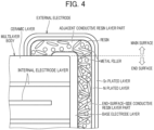
- FIG. 4 is a schematic cross-sectional view showing the structure of an external electrode.
- FIG. 5A is a cross-sectional view along the line II-II in FIG. 1 showing the structure of an internal electrode layer of the multilayer ceramic capacitor according to an embodiment of the present invention in which counter electrode is divided into two
- FIG.5B is a cross-sectional view along the line II-II in FIG.
- FIG.5C is a cross-sectional view along the line II-II in FIG. 1 showing the structure of an internal electrode layer of the multilayer ceramic capacitor according to an embodiment of the present invention in which counter electrode is divided into four.
- FIG. 1 is an external perspective view showing an example of a multilayer ceramic capacitor as a multilayer ceramic electronic component according to an embodiment of the present invention.
- FIG. 2 is a cross-sectional view along the line II-II in FIG. 1 .
- FIG. 3 is a cross-sectional view along the line III-III in FIG. 1 .
- FIG. 4 is a schematic cross-sectional view showing the structure of an external electrode.
- the multilayer ceramic capacitor 10 includes a rectangular parallelepiped-shape multilayer body 12, and an external electrode 30 arranged on both ends of the multilayer body 12.
- the multilayer body 12 has a plurality of laminated ceramic layers 14, and a plurality of internal electrode layers 16 laminated on the ceramic layer 14. Furthermore, the multilayer body 12 has a first main surface 12a and a second main surface 12b opposing in a height direction x, a first lateral surface 12c and a second lateral surface 12d opposing in a width direction y orthogonal or substantially orthogonal to the height direction x, and a first end surface 12e and a second end surface 12f opposing in a length direction z orthogonal or substantially orthogonal to the height direction x and width direction y. This multilayer body 12 is rounded at corner portions and ridge portions.
- corner portion is a portion at which three adjacent surfaces of the multilayer body intersect
- ridge portion is a portion at which two adjacent surface of the multilayer body intersect.
- unevenness or the like may be formed in a part or the entirety of the first main surface 12a and second main surface 12b, the first lateral surface 12c and second lateral surface 12d and first end surface 12e and second end surface 12f.
- the ceramic layer 14 and internal electrode layer 16 are laminated in the height direction x.
- the multilayer body 12 in a lamination direction linking first main surfaces 12a and second main surface 12b, includes an effective layer part 18 at which a plurality of internal electrode layers 16 are opposing, a first outer layer portion 20a formed from a plurality of ceramic layers 14 positioned between the internal electrode layer 16 located most to the side of the first main surface 12a and the first main surface 12a, and a second outer layer portion 20b formed from a plurality of ceramic layers 14 positioned between the internal electrode layer 16 located most to the side of the second main surface 12b and the second main surface 12b.
- the first outer layer portion 20a is positioned at the side of the first main surface 12a of the multilayer body 12, and is an aggregate body of a plurality of ceramic layers 14 located between the first main surface 12a and the internal electrode layer 16 closest to the first main surface 12a.
- the second outer layer portion 20b is positioned at the second main surface 12b side of the multilayer body 12, and is an aggregate body of a plurality of the ceramic layers 14 located between the second main surface 12b and the internal electrode layer 16 closest to the second main surface 12b.
- the number of laminated ceramic layers 14 is not particularly limited; however, it is preferable to include the first outer layer portion 20a and second outer layer portion 20b, and be at least 10 and no more than 700.
- the thickness of the ceramic layer 14 is preferably at least 0.5 um and no more than 15.0 ⁇ m.
- the dimensions of the multilayer body 12 is not particularly limited; however, it is preferably dimensions not exceeding the dimensions of the multilayer ceramic capacitor 10, including the thickness of the external electrode 30.
- the ceramic layer 14, for example, can be formed by a dielectric material as the ceramic material.
- a dielectric material for example, it is possible to use a dielectric ceramic containing components such as BaTiO 3 , CaTiO 3 , SrTiO 3 or CaZrO 3 .
- a material made by adding auxiliary components in a smaller content than the main component such as Mn compound, Fe compound, Cr compound, Co compound and Ni compound, for example, may be used according to the desired characteristics of the multilayer body 12.
- the multilayer ceramic electronic component functions as the piezoelectric component.
- the piezoelectric ceramic material for example, a PZT (lead zirconate titanate)-based ceramic material or the like can be exemplified.
- the multilayer ceramic electronic component functions as a thermistor.
- the semiconductor ceramic material for example, a spinel ceramic material or the like can be exemplified.
- the multilayer ceramic electronic component functions as an inductor.
- the internal electrode layer 16 becomes a coil-like conductor or the like.
- the magnetic ceramic material for example, a ferrite ceramic material or the like can be exemplified.
- the thickness of the fired ceramic layer 14 is preferably at least 0.5 um and no more than 15 um.
- the number of laminated ceramic layers 14 is preferably at least 10 and no more than 700. It should be noted that this number of ceramic layers 14 is the total number of the number of ceramic layers 14 of the effective layer part 18, and the number of ceramic layers 14 of the first outer layer portion 20a and second outer layer portion 20b.
- the multilayer body 12 has, as the plurality of internal electrode layers 16, a plurality of first internal electrode layers 16a and a plurality of second internal electrode layers 16b which are substantially rectangular, for example.
- the plurality of first internal electrode layers 16a and plurality of second internal electrode layers 16b are embedded so as to be alternately arranged at equal intervals sandwiching the ceramic layer 14 along the height direction x of the multilayer body 12.
- the first internal electrode layer 16a is arranged on a plurality of the ceramic layers 14, and is positioned inside of the multilayer body 12.
- the first internal electrode layer 16a has a first counter electrode part 22a opposing the second internal electrode layer 16b, and a first extraction electrode part 24a positioned on one end side of the first internal electrode layer 16a from the first counter electrode part 22a until a first end surface 12e of the multilayer body 12.
- the first extraction electrode part 24a has an end part thereof drawn to the surface of the first end surface 12e, and is exposed from the multilayer body 12.
- the shape of the first counter electrode part 22a of the first internal electrode layer 16a is not particularly limited, but is preferably a rectangular shape in a plan view.
- the corner portions in a plan view may be rounded, or the corner portions may be formed obliquely in a plan view (tapered).
- it may be a tapered shape in a plan view with an incline as approaching either direction.
- the shape of the first extraction electrode 24a of the first internal electrode layer 16a is not particularly limited, but is preferably a rectangular shape in a plan view.
- the corner portions in a plan view may be rounded, or the corner portions may be formed obliquely in a plan view (tapered).
- it may be a tapered shape in a plan view with an incline as approaching either direction.
- the width of the first counter electrode part 22a of the first internal electrode layer 16a and the width of the first extraction electrode layer 24a of the first internal electrode layer 16a may be formed as the same width, or may be formed so that the width of either is narrower.
- the second internal electrode layer 16b is arranged on the plurality of ceramic layers 14, and is located inside of the multilayer body 12.
- the second internal electrode layer 16b has a second counter electrode part 22b opposing the first internal electrode layer 16a, and a second extraction electrode part 24b located at one end side of the second internal electrode layer 16b from the second counter electrode part 22b until the second end surface 12f of the multilayer body 12.
- the second extraction electrode part 24b has an end thereof drawn out to a surface of the second end surface 12f, and exposed from the multilayer body 12.
- the shape of the second counter electrode part 22b of the second internal electrode layer 16b is not particularly limited, but is preferably a rectangular shape in a plan view.
- the corner portions in a plan view may be rounded, or the corner portions may be formed obliquely in a plan view (tapered).
- it may be a tapered shape in a plan view with an incline as approaching either direction.
- the shape of the second extraction electrode part 24b of the second internal electrode layer 16b is not particularly limited, but is preferably a rectangular shape in a plan view.
- the corner portions in a plan view may be rounded, or the corner portions may be formed obliquely in a plan view (tapered).
- it may be a tapered shape in a plan view with an incline as approaching either direction.
- the width of the second counter electrode part 22b of the second internal electrode layer 16b, and the width of the second extraction electrode part 24b of the second internal electrode layer 16b may be formed at the same width, or may be formed with the width of either one narrower.
- the multilayer body 12 includes an end part (hereinafter referred to as "L gap") 28 of the multilayer body 12 formed between an end part of the first internal electrode layer 16a on an opposite side to the first extraction electrode part 24a and the second end surface 12f, and between an end part of the second internal electrode layer 16b on an opposite side to the second extraction electrode part 24b and the first end surface 12e.
- L gap an end part
- the multilayer body 12 includes a lateral part (hereinafter referred to as "W gap") 26 of the multilayer body 12 formed between an end in the width direction y of the first counter electrode part 22a and second counter electrode part 22b, and the first lateral surface 12c, and between the other end in the width direction y of the first counter electrode part 22a and second counter electrode part 22b and the second lateral surface 12d.
- W gap lateral part
- the first internal electrode layer 16a and second internal electrode layer 16b can be constituted by appropriate conductive material such as metals such as Ni, Cu, Ag, Pd and Au, and an alloys containing at least one of these metals such as an Ag-Pd alloy.
- each of the internal electrode layers 16, i.e. first internal electrode layer 16a and second internal electrode layer 16b is preferably at least 0.2 um and no more than 2.0 um.
- the number of the first internal electrode layers 16a and second internal electrode layers 16b is preferably at least 10 and no more than 700 combined.
- the external electrode 30 is arranged on the first end surface 12e side and the second end surface 12f side of the multilayer body 12.
- the external electrode 30 includes the first external electrode 30a and second external electrode 30b.
- the first external electrode 30a is connected to the first internal electrode layer 16a, and is arranged at the surface of at least the first end surface 12e.
- the first external electrode 30a is arranged extending from the first end surface 12e of the multilayer body 12 to a part of the first main surface 12a and a part of the second main surface 12b, as well as a part of the first lateral surface 12c and part of the second lateral surface 12d.
- the first external electrode 30a is electrically connected with the first extraction electrode part 24a of the first internal electrode layer 16a.
- the second external electrode 30b is connected to the second internal electrode layer 16b, and is arranged on at least the surface of the second end surface 12f.
- the second external electrode 30b is arranged to extend from the second end surface 12f to a part of the first main surface 12a and a part of the second main surface 12b, as well as a part of the first lateral surface 12c and a part of the second lateral surface 12d.
- the second external electrode 30b is electrically connected with the second extraction electrode part 24b of the second internal electrode layer 16b.
- electrostatic capacitance is formed by the first counter electrode part 22a of the first internal electrode layer 16a and the second counter electrode part 22b of the second internal electrode layer 16b opposing each other via the ceramic layer 14. For this reason, it is possible to obtain electrostatic capacitance between the first external electrode 30a to which the first internal electrode layer 16a is connected, and the second external electrode 30b to which the second internal electrode layer 16b is connected, whereby the characteristics of a capacitor are expressed
- the multilayer body 12 shown in FIG. 1 may be made a structure in which a floating internal electrode layer 16c which is not drawn out is provided to either of the first end surface 12e and second end surface 12f, in addition to the first internal electrode layer 16a and second internal electrode layer 16b, and the counter electrode part 22c is divided into many by the floating electrode layer 16c, as shown in FIGS. 5A to 5C .
- a floating internal electrode layer 16c which is not drawn out is provided to either of the first end surface 12e and second end surface 12f, in addition to the first internal electrode layer 16a and second internal electrode layer 16b, and the counter electrode part 22c is divided into many by the floating electrode layer 16c, as shown in FIGS. 5A to 5C .
- it is a two-portion structure shown in FIG. 5B , three-portion structure shown in FIG. 5B , or a four-portion structure such as that shown in FIG. 5C , and it goes without saying may be a four or more-portion structure.
- the external electrode 30 includes: a base electrode layer 32 including a metal component and glass component, a conductive resin layer 34 containing a metal component and resin component arranged on the base electrode layer 32, and a plated layer 36 arranged on the conductive resin layer 34.
- the first external electrode 30a includes: a first base electrode layer 32a containing the metal component and glass component, and a first conductive resin layer 34a containing a metal component and resin component arranged on the first base electrode layer 32a, and a first plated layer 36a arranged on the first conductive resin layer 34a.
- the second external electrode 30b includes: a second base electrode layer 32b containing a metal component and glass component, a second conductive resin layer 34b containing a metal component and resin component arranged on the second base electrode layer 32b, and a second plated layer 36b arranged on the second conductive resin layer 34b.
- the base electrode layer 32 has a first base electrode layer 32a and second base electrode layer 32b.
- the first base electrode layer 32a is connected to the first internal electrode layer 16a, and arranged at the surface of the first end surface 12e.
- the first base electrode layer 32a is arranged extending from the first end surface 12e to a part of the first main surface 12a and second main surface 12b, as well as a part of the first lateral surface 12c and part of the second lateral surface 12d.
- the first base electrode layer 32a is electrically connected with the first extraction electrode part 24a of the first internal electrode layer 16a.
- the second base electrode layer 32b is connected to the second internal electrode layer 16b, and arranged at the surface of the second end surface 12f.
- the second base electrode layer 32b extends from the second end surface 12f to be arranged at a part of the first main surface 12a and part of the second main surface 12b, as well as a part of the first lateral surface 12c and part of the second lateral surface 12d.
- the second base electrode layer 32b is electrically connected with the second extraction electrode part 24b of the second internal electrode layer 16b.
- the base electrode layer 32 includes at least one selected from a fired layer, thin film layer or the like.
- a fired layer thin film layer or the like.
- the fired layer contains a glass component and a metal component.
- the glass component of the fired layer contains at least one selected from B, Si, Ba, Mg, Al, Li or the like.
- the metal component of the fired layer for example, contains at least one selected from Cu, Ni, Ag, Pd, Ag-Pd alloy, Au or the like.
- the fired layer is a layer made by coating a conductive paste containing a glass component and metal component on the multilayer body 12 and firing.
- the fired layer may be made by simultaneously firing a multilayer chip having an internal electrode layer 16 and ceramic layer 14 and a conductive paste coated on the multilayer chip, or may be made by firing a multilayer chip having an internal electrode layer 16 and ceramic layer 14 to obtain a multilayer body, followed by firing a conductive paste on the multilayer body.
- the fired layer in the case of simultaneously firing the multilayer chip having the internal electrode layer 16 and ceramic layer 14, and the conductive paste coated on the multilayer chip, the fired layer is preferably formed by firing a layer obtained by adding a ceramic component in place of the glass component.
- the fired layer may be multiple layers.
- the base electrode layer 32 may contain both the glass component and ceramic component.
- the ceramic component contained in the base electrode layer 32 may use the same type of ceramic material as the ceramic layer 14, or may use a different type of ceramic material.
- the ceramic component for example, contains at least one selected from BaTiO 3 , CaTiO 3 , (Ba,Ca)TiO 3 , SrTiO 3 , CaZrO 3 or the like.
- the thickness in the length direction z linking the first end surface 12e and second end surface 12f at a central part in the height direction x of the first base electrode layer 32a positioned at the first end surface 12e is preferably on the order of at least 2 um and no more than 220 um.
- the thickness in the length direction z linking the first end surface 12e and second end surface 12f at the central part in the height direction x of the second base electrode layer 32b positioned at the second end surface 12f is preferably on the order of at least 2 um and no more than 220 ⁇ m.
- the thickness in the height direction x linking the first main surface 12a and second main surface 12b at the central part in the length direction z linking the first end surface 12e and second end surface 12f of the first base electrode layer 32a located at part of the first main surface 12a and second main surface 12b, for example, is preferably on the order of at least 3 um and no more than 40 um.
- the thickness in the height direction x linking the first main surface 12a and second main surface 12b at a central part in the length direction z linking the first end surface 12e and second end surface 12f of the second base electrode layer 32b located at a part of the first main surface 12a and second main surface 12b, for example, is preferably on the order of at least 3 um and no more than 40 ⁇ m.
- the thickness in the width direction y linking the first lateral surface 12c and second lateral surface 12d at a central part in the length direction z linking the first end surface 12e and second end surface 12f of the first base electrode layer 32a located at a part of the first lateral surface 12c and second lateral surface 12d is preferably on the order of at least 3 um and no more than 40 um.
- the thickness in the width direction y linking the first lateral surface 12c and second lateral surface 12d in the central part in the length direction z linking the first end surface 12e and second end surface 12f of the second base electrode layer 32b positioned at part of the first lateral surface 12c and second lateral surface 12d is preferably on the order of at least 3 um and no more than 40 ⁇ m.
- the thin layer is a layer no more than 1 um formed by a thin film formation method such as sputtering or vapor deposition, and in which metal particles are deposited.
- the conductive resin layer 34 is arranged on the base electrode layer 32, and contains a resin component and metal component.
- the conductive resin layer 34 is arranged so as to completely cover the base electrode layer 32.
- the conductive resin layer 34 has a first conductive resin layer 34a and second conductive resin layer 34b.
- the first conductive resin layer 34a is arranged on the first base electrode layer 32a, and still the first conductive resin layer 34a is arranged so as to completely cover the first base electrode layer 32a, and the end part of the first conductive resin layer 34a contacts the multilayer body 12.
- the second conductive resin layer 34b is arranged on the second based electrode layer 32b, and still the second conductive resin layer 34b is arranged so as to completely cover the second base electrode layer 32b, and the end part of the second conductive resin layer 34b contacts the multilayer body 12.
- the conductive resin layer 34 due to containing a thermosetting resin which is a resin component, for example, has more flexibility than the base electrode layer 32 consisting of a plated film, and/or a fired product of a metal component and glass component. For this reason, even in a case of flexural stress acting on the mounting substrate, or an impact caused by physical shock or thermal cycling being applied to the multilayer ceramic capacitor 10, the conductive resin layer 34 will function as a buffer layer, and it is possible to prevent cracks from occurring in the multilayer ceramic capacitor 10.
- thermosetting resin of the conductive resin layer 34 for example, it is possible to use various known thermosetting resins such as epoxy resin, phenoxy resin, phenolic resin, urethane resin, silicone resin, polyimide resin. Thereamong, an epoxy resin superior in heat resistance, moisture resistance and adhesion is one of the most appropriate resins.
- the conductive resin layer 34 preferably contains a curing agent together with the thermosetting resin.
- the curing agent in the case of using an epoxy resin as the base resin, it is possible to use various known compounds such as phenol-based, amine-based, acid anhydride-based, imidazole-based, active ester-based and amideimide-based compounds as the curing agent of the epoxy resin.
- the metal component contained in the conductive resin layer 34 is a metal filler.
- the metal filler can employ Ag, Cu, Ni, Sn, Bi or an alloy containing these.
- metal powder with Ag coating on the surface of the metal powder Upon using a powder coated with Ag on the surface of the metal powder, it is preferable to use Cu, Ni, Sn, Be or alloy powders of these as the metal powder.
- Ag is suited to an electrode material due to having the lowest specific resistance among the metals, and Ag is a noble metal and has high weather resistance without oxidizing. In addition, this is because it is becomes possible to make the base metal cheaper, while maintaining the above characteristics of Ag.
- the metal filler contained in the conductive resin layer 34 it is possible to use a filler made by conducting an antioxidation treatment on Cu or Ni.
- the metal filler contained in the conductive resin layer 34 it is possible to use a metal powder with Sn, Ni, or Cu coated on the surface of the metal powder.
- metal powder coated with Sn, Ni, Cu on the surface of the metal powder it is preferable to use Ag, Cu, Ni, Sn, Bi or an alloy powder of these as the metal powder.
- the shape of the metal filler contained in the conductive resin layer 34 is not particularly limited.
- the metal filler may be spherical, flat, or the like. In addition, it may be mixing spherical metal powder and flat metal powder.
- the average particle size of the metal filler contained in the conductive resin layer 34 is not particularly limited.
- the average particle size of the metal filler for example, may be on the order of at least 0.3 um and no more than 10.0 ⁇ m.
- the measurement method of the average particle size of metal filler contained in the conductive resin layer 34 can calculate using a laser diffraction particle size measuring method based on ISO 13320 irrespective of the shape of the filler.
- the metal filler contained in the conductive resin layer 34 mainly accounts for the conductivity of the conductive resin layer 34. More specifically, the energizing path is formed inside of the conductive resin layer 34 by the metal fillers making contact.
- the first conductive resin layer 34a has a first end-surface-side conductive resin layer part 34a 1 positioned on the first end surface 12e, and a first adjacent conductive resin layer part 34a 2 positioned to extend from an end part of the first end-surface-side conductive resin layer part 34a 1 portion to a part on the first main surface 12a, a part on the second main surface 12b, a part on the first lateral surface 12c and a part on the second lateral surface 12d.
- the second conductive resin layer 34b has a second end-surface-side conductive resin layer part 34b 1 positioned on the first end surface 12f, and a second adjacent conductive resin layer part 34b 2 positioned to extend from an end part of the first end-surface-side conductive resin layer part 34a 1 portion to a part on the first main surface 12a, a part on the second main surface 12b, a part on the first lateral surface 12c and a part on the second lateral surface 12d.
- the resin amount contained in the first adjacent conductive resin layer part 34a 2 is greater than the resin amount contained in the first end-surface-side conductive resin layer part 34a 1
- the resin amount contained in the second adjacent conductive resin layer part 34b 2 is greater than the resin amount contained in the second end-surface-side conductive resin layer part 34b 1 .
- the content ratio of resin component contained in the first adjacent conductive resin layer part 34a 2 is greater than the content ratio of resin component contained in the first end-surface-side conductive resin layer part 34a 1
- the content ratio of resin component contained in the second adjacent conductive resin layer part 34b 2 is greater than the content ratio of resin component contained in the second end-surface-side conductive resin layer part 34b 1 .
- first adjacent conductive resin layer part 34a 2 and the second adjacent conductive resin layer part 34b 2 having an abundant amount of resin, since it becomes possible to maintain sufficient elasticity, upon stress from impact when dropping, or deflective stress occurring by being subject to thermal cycling and the mounting substrate thermally expanding and contracting being generated, for the stress transmitted to the mounting substrate (distortion of mounting substrate), it is possible to peel off between the first base electrode layer 32a and first adjacent conductive resin layer part 34a2, or between the first plated layer 36a and first adjacent conductive resin layer part 34a2 with the starting point of the leading end of the first adjacent conductive resin layer part 34a 2 , and possible to fracture cohesion inside of the first adjacent conductive resin layer part 34a 2 , and similarly, it is possible to peel off between the second base electrode layer 32b and second adjacent conductive resin layer part 34b 2 , or between the second plated layer 36b and second adjacent conductive resin layer part 34b 2 with the starting point of the leading end of the second adjacent conductive resin layer part 34b
- the present invention makes it possible to effectively exhibit the characteristics of both of these.
- the content ratio of resin component in the first end-surface-side conductive resin layer part 34a 1 and the second end-surface-side conductive resin layer part 34b 1 , when defining the total amount of the resin component and metal component as 100%, is at least 10% and no more than 60%.
- the conductive resin layer 34 generally causes the metal filler particles to contact, by trying to pull the metal filler particles together by the resin contracting upon curing of the conductive resin layer 34.
- the measurement method of the content ratio of resin component in the first end-surface-side conductive resin layer part 34a 1 and the second end-surface-side conductive resin layer part 34b 1 can be measured in a cross section as shown below.
- polishing is started from the first lateral surface 12c or second lateral surface 12d of the multilayer ceramic capacitor 10, and the central part in the height direction x of the first end-surface-side conductive resin layer part 34a 1 on the side of the first end surface 12e or the second end-surface-side conductive resin layer part 34b 1 on the side of the second end surface 12f is confirmed in the LT plane polished to a position that is 1/2W in the width direction y linking the first lateral surface 12c and second lateral surface 12d.
- polishing is started from the first main surface 12a or second main surface 12b of the multilayer ceramic capacitor 10, and the central part in the width direction y of the first end-surface-side conductive resin layer part 34a 1 on the side of the first end surface 12e or the second end-surface-side conductive resin layer part 34b 1 on the side of the second end surface 12f is confirmed in the LW plane polished to a position that is 1/2T in the height direction x linking the first main surface 12a and second main surface 12b.
- thermosetting resin metal component (metal filler), voids).
- photographed image is binarized into the thermosetting resin and other by image analysis software, and it is possible to obtain the content ratio of resin component in the first end-surface-side conductive resin layer part 34a 1 and the second end-surface-side conductive resin layer part 34b 1 .
- the content ratio of metal component in the first end-surface-side conductive resin layer part 34a 1 and the second end-surface-side conductive resin layer part 34b 1 , upon defining the total amount of resin component and metal component as 100%, is preferably at least 40% and no more than 90%. It thereby becomes possible to improve the conductivity in the first end-surface-side conductive resin layer part 34a 1 and the second end-surface-side conductive resin layer part 34b 1 having abundant metal filler constituting the metal component, a result of which the ESR of the multilayer ceramic component 10 declines.
- the ESR may deteriorate.
- the conductive resin layer 34 generally causes the metal filler particles to contact, by trying to pull the metal filler particles by the resin contracting upon curing of the conductive resin layer 34.
- the measurement method of the content ratio of metal component in the first end-surface-side conductive resin layer part 34a 1 and the second end-surface-side conductive resin layer part 34b 1 can measure in a cross section, as shown below.
- polishing is started from the first lateral surface 12c or second lateral surface 12d of the multilayer ceramic capacitor 10, and the central part in the height direction x of the first end-surface-side conductive resin layer part 34a 1 on the side of the first end surface 12e or the second end-surface-side conductive resin layer part 34b 1 on the side of the second end surface 12f is confirmed in the LT plane polished to a position that is 1/2W in the width direction y linking the first lateral surface 12c and second lateral surface 12d.
- polishing is started from the first main surface 12a or second main surface 12b of the multilayer ceramic capacitor 10, and the central part in the width direction y of the first end-surface-side conductive resin layer part 34a 1 on the side of the first end surface 12e or the second end-surface-side conductive resin layer part 34b 1 on the side of the second end surface 12f is confirmed in the LW plane polished to a position that is 1/2T in the height direction x linking the first main surface 12a and second main surface 12b.
- thermosetting resin metal component (metal filler), voids).
- photographed image is binarized into the thermosetting resin and other by image analysis software, and it is possible to obtain the content ratio of metal component in the first end-surface-side conductive resin layer part 34a 1 and the second end-surface-side conductive resin layer part 34b 1 .
- the content ratio of resin component in the first adjacent conductive resin layer part 34a 2 and the second adjacent conductive resin layer part 34b 2 , upon defining the total amount of resin component and metal component as 100%, is preferably at least 40% and no more than 60%.
- the first base electrode layer 32a and first adjacent conductive resin layer part 34a 2 at which stress tends to act, since it is thereby possible to impart sufficient elasticity, upon stress due to impact when falling, or deflection stress generated by being subject to thermal cycling and the mounting substrate thermally expanding being generated, for the stress transmitted to the mounting substrate (mounting substrate distortion), it is possible to peel off between the first base electrode layer 32a and first adjacent conductive resin layer part 34a 2 , or between the first plated layer 36a and first adjacent conductive resin layer part 34a 2 with the starting point of the leading end of the arranged portion of the first adjacent conductive resin layer part 34a 2 , and similarly, it is possible to peel off between the second base electrode layer 32b and second adjacent conductive resin layer part 34b 2 ,
- the content ratio of resin component in the first adjacent conductive resin layer part 34a 2 and the second adjacent conductive resin layer part 34b 2 upon defining the total amount of resin component and metal component as 100%, in the case of being smaller than 40%, the content ratio of metal component in the first adjacent conductive resin layer part 34a 2 and the second adjacent conductive resin layer part 34b 2 increases.
- the metal filler comes to have a higher value.
- the entire portion of the conductive resin layer 34 hardens, and even in the case of stress from impact when dropping, or deflective stress occurring by being subject to thermal cycling and the mounting substrate thermally expanding and contracting being generated, for the stress transmitted to the mounting substrate (distortion of mounting substrate), it will not be possible to peel off between the first base electrode layer 32a and first adjacent conductive resin layer part 34a 2 , or between the first plated layer 36a and first adjacent conductive resin layer part 34a 2 , with the starting point of the leading end of the arranged portion of the first adjacent conductive resin layer part 34a2, and similarly, it will not be possible to peel off between the second base electrode layer 32b and second adjacent conductive resin layer part 34b 2 , or between the second plated layer 36b and second adjacent conductive resin layer part 34b 2 with the starting point of the leading end of the arranged portion of the second adjacent conductive resin layer
- the content ratio of resin component in the first adjacent conductive resin layer part 34a 2 and the second adjacent conductive resin layer part 34b 2 upon defining the total amount of resin component and metal component as 100%, in the case of being greater than 90%, since the resin amount in the first adjacent conductive resin layer part 34a 2 and the second adjacent conductive resin layer part 34b 2 increases, the metal filler exposed at the surface of the first adjacent conductive resin layer part 34a 2 and the second adjacent conductive resin layer part 34b 2 decreases.
- plating formation is hindered.
- plating formation is hindered, a portion without plating formation occurs, and thus makes a plated layer in which several defective parts exist discontinuously.
- the measurement method of the content ratio of resin component in the first adjacent conductive resin layer part 34a 2 and the second adjacent conductive resin layer part 34b 2 can measure in a cross section, as shown below.
- polishing is started from the first lateral surface 12c or second lateral surface 12d of the multilayer ceramic capacitor 10, and the central part in the length direction z of the first adjacent conductive resin layer part 34a 2 on the first main surface 12a side or second main surface 12b side, or the second adjacent conductive resin layer part 34b 2 on the first main surface 12a side or second main surface 12b side is confirmed in the LT plane polished to a position which is 1/2W in the width direction y linking the first lateral surface 12c and second lateral surface 12d.
- polishing is started from the first main surface 12a or second main surface 12b of the multilayer ceramic capacitor 10, and the central part in the length direction z of the first adjacent conductive resin layer part 34a 2 on the first lateral surface 12c side or second lateral surface 12d side, or the second adjacent conductive resin layer part 34b 2 on the first lateral surface 12c side or second lateral surface 12d side is confirmed, in the LW plane polished to a position which is 1/2T in the height direction x linking the first main surface 12a and second main surface 12b.
- thermosetting resin metal component (metal filler), voids).
- photographed image is binarized into the thermosetting resin and other by image analysis software, and it is possible to obtain the content ratio of resin component in the first adjacent conductive resin layer part 34a 2 and the second adjacent conductive resin layer part 34b 2 .
- the content ratio of metal component in the first adjacent conductive resin layer part 34a 2 and the second adjacent conductive resin layer part 34b 2 , upon defining the total amount of the resin component and metal components as 100%, is preferably at least 10% and no more than 60%. It is thereby possible to secure conduction, and upon stress from impact when dropping, or deflective stress occurring by being subject to thermal cycling and the mounting substrate thermally expanding and contracting being generated, for the stress transmitted to the mounting substrate (distortion of mounting substrate), it is possible to peel off between the first base electrode layer 32a and first adjacent conductive resin layer part 34a 2 , or between the first plated layer 36a and first adjacent conductive resin layer part 34a 2 with the starting point of the leading end of the arranged portion of the first adjacent conductive resin layer part 34a 2 , and similarly, it is possible to peel off between the second base electrode layer 32b and second adjacent conductive resin layer part 34b 2 , or between the second plated layer 36b and second adjacent conductive resin layer part 34b 2 with the starting point of the leading end of the
- the metal filler exposed at the surface of the first adjacent conductive resin layer part 34a 2 and the second adjacent conductive resin layer part 34b 2 decreases.
- the content ratio of the metal component in the first adjacent conductive resin layer part 34a 2 and the second adjacent conductive resin layer part 34b 2 upon defining the total amount of the resin component and metal component as 100%, in the case of being greater than 60%, the content ratio of the metal component in the first adjacent conductive resin layer part 34a 2 and the second adjacent conductive resin layer part 34b 2 increases.
- the metal filler comes to have a higher value.
- the entire portion of the conductive resin layer 34 hardens, and even in the case of stress from impact when dropping, or deflective stress occurring by being subject to thermal cycling and the mounting substrate thermally expanding and contracting being generated, for the stress transmitted to the mounting substrate (distortion of mounting substrate), it is not possible to peel off between the first base electrode layer 32a and first adjacent conductive resin layer part 34a 2 , or between the first plated layer 36a and first adjacent conductive resin layer part 34a 2 with the starting point of the leading end of the arranged portion of the first adjacent conductive resin layer part 34a 2 , and similarly, it is not possible to peel off between the second base electrode layer 32b and second adjacent conductive resin layer part 34b 2 , or between the second plated layer 36b and second adjacent conductive resin layer part 34b 2 with the starting point of the leading end of the arranged portion of the second adjacent conductive resin layer part 34
- the measurement method of the content ratio of the metal component in the first adjacent conductive resin layer part 34a 2 and the second adjacent conductive resin layer part 34b 2 can measure in a cross section, as shown below.
- polishing is started from the first lateral surface 12c or second lateral surface 12d of the multilayer ceramic capacitor 10, and the central part in the height direction x of the first adjacent conductive resin layer part 34a 2 on the first main surface 12a side or second main surface 12b side, or the second adjacent conductive resin layer part 34b 2 on the first main surface 12a side or second main surface 12b side is confirmed in the LT plane polished to a position which is 1/2W in the width direction y linking the first lateral surface 12c and second lateral surface 12d.
- polishing is started from the first main surface 12a or second main surface 12b of the multilayer ceramic capacitor 10, and the central part in the length direction z of the first adjacent conductive resin layer part 34a 2 on the first lateral surface 12c side or second lateral surface 12d side, or the second adjacent conductive resin layer part 34b 2 on the first lateral surface 12c side or second lateral surface 12d side is confirmed, in the LW plane polished to a position which is 1/2T in the height direction x linking the first main surface 12a and second main surface 12b.
- thermosetting resin metal component (metal filler), voids).
- photographed image is binarized into the thermosetting resin and other by image analysis software, and it is possible to obtain the content ratio of metal component in the first adjacent conductive resin layer part 34a 2 and the second adjacent conductive resin layer part 34b 2 .
- the thickness in the conductive resin layer 34 positioned at a central part in the height direction x of the multilayer body 12 located at the first end surface 12e and second end surface 12f, for example, is preferably on the order of at least 20.0 um and no more than 150.0 ⁇ m.
- the thickness of the conductive resin layer 34 at a central part in the length direction z of the conductive resin layer positioned at the first main surface 12a and second main surface 12b, and first lateral surface 12c and second lateral surface 12d is preferably on the order of at least 5.0 um and no more than 40.0 ⁇ m.
- the conductivity (resistance) in the first end-surface-side conductive resin layer part 34a 1 and the second end-surface-side conductive resin layer part 34b 1 is preferably at least 5 ⁇ cm and no more than 25 ⁇ cm, and the conductivity (resistance) in the first adjacent conductive resin layer part 34a 2 and the second adjacent conductive resin layer part 34b 2 is preferably at least 20 ⁇ cm and no more than 150 ⁇ cm. It is thereby possible to decrease the ESR of the multilayer ceramic capacitor 10.
- the indentation elastic modulus of the first end-surface-side conductive resin layer part 34a 1 and the second end-surface-side conductive resin layer part 34b 1 is preferably at least 15 GPa and no more than 21 GPa
- the indentation elastic modulus of the first adjacent conductive resin layer part 34a 2 and the second adjacent conductive resin layer part 34b 2 is preferably at least 12 GPa and no more than 15 GPa. It is thereby possible to relieve the stress on the multilayer body 12, whereby it becomes possible to suppress cracking in the multilayer body 12, and possible to improve the mechanical strength of the multilayer ceramic capacitor 10.
- the storage modulus of the first adjacent conductive resin layer part 34a 2 and the second adjacent conductive resin layer part 34b 2 is preferably at least 6 GPa and no more than 8 GPa, and the storage modulus of the first end-surface-side conductive resin layer part 34a 1 and the second end-surface-side conductive resin layer part 34b 1 is preferably at least 8 GPa and no more than 10 GPa. It is thereby possible to relieve the stress on the multilayer body 12, whereby it becomes possible to suppress cracking in the multilayer body 12, and possible to improve the mechanical strength of the multilayer ceramic capacitor 10.
- the loss modulus of the first adjacent conductive resin layer part 34a 2 and the second adjacent conductive resin layer part 34b 2 is preferably at least 0.2 GPa and no more than 0.4 GPa, and the loss modulus of the first end-surface-side conductive resin layer part 34a 1 and the second end-surface-side conductive resin layer part 34b 1 is preferably at least 0.4 GPa and no more than 0.5 GPa. It is thereby possible to relieve the stress on the multilayer body 12, whereby it becomes possible to suppress cracking in the multilayer body 12, and possible to improve the mechanical strength of the multilayer ceramic capacitor 10.
- the hardness of the first adjacent conductive resin layer part 34a 2 and the second adjacent conductive resin layer part 34b 2 is preferably at least 0.1 GPa and no more than 0.3 GPa, and the hardness of the first end-surface-side conductive resin layer part 34a 1 and the second end-surface-side conductive resin layer part 34b 1 is preferably at least 0.2 GPa and no more than 0.7 GPa. It is thereby possible to relieve the stress on the multilayer body 12, whereby it becomes possible to suppress cracking in the multilayer body 12, and possible to improve the mechanical strength of the multilayer ceramic capacitor 10.
- the first plated layer 36a and second plated layer 36b which are the plated layers 36 arranged on the based electrode layer 32, will be explained by referencing FIGS. 2 and 3 .
- the first plated layer 36a and second plated layer 36b for example, contain at least one selected from Cu, Ni, Sn, Ag, Pd, Ag-Pd alloy, Au or the like.
- the first plated layer 36a is arranged so as to completely cover the first conductive resin layer 34a.
- the second plated layer 36b is arranged so as to completely cover the second conductive resin layer 34b.
- the first plated layer 36a and second plated layer 36b may be formed from a plurality of layers.
- the plated layer 36 is preferably a two-layer structure of a lower plated layer (Ni plated layer) from Ni plating formed on the conductive resin layer 34, and an upper plated layer (Sn plated layer) from Sn plating formed on the first lower plated layer.
- the first plated layer 36a has a first lower plated layer, and a first upper plated layer positioned on the surface of the lower plated layer.
- the second plated layer 36b has a second lower plated layer, and a second upper plated layer positioned on the surface of the second lower plated layer.
- the lower plated layer from Ni plating is used for preventing the base electrode layer 32 or conductive resin layer 34 from being eroded by solder upon mounting to the multilayer ceramic capacitor 10, and the upper plated layer from Sn plating is used so as to configure to be able to easily mount by improving the wettability of solder upon mounting the multilayer ceramic capacitor 10.
- the thickness per layer of plated layer is preferably at least 1.0 um and no more than 15.0 um.
- the dimension in the length direction z of the multilayer ceramic capacitor 10 including the multilayer body 12, first external electrode 30a and second external electrode 30b is defined as the L dimension
- the dimension in the height direction x of the multilayer ceramic capacitor 10 including the multilayer body 12, first external electrode 30a and second external electrode 30b is defined as the T dimension
- the dimension in the width direction y of the multilayer ceramic capacitor 10 including the multilayer body 12, first external electrode 30a and second external electrode 30b is defined as the W dimension.
- the L dimension in the length direction is at least 0.2 mm and no more than 10.0 mm
- the W dimension in the width direction y is at least 0.1 mm and no more than 10.0 mm
- the T dimension in the height direction x is at least 0.1 mm and no more than 10.0 mm.
- the dimensions of the multilayer ceramic capacitor 10 can be measured by a microscope.
- the content ratio of resin component contained in the first adjacent conductive resin layer part 34a 2 is greater than the content ratio of resin component contained in the first end-surface-side conductive resin layer part 34a 1
- the content ratio of resin component contained in the second adjacent conductive resin layer part 34b 2 is greater than the content ratio of resin component contained in the second end-surface-side conductive resin layer part 34b 1 .
- the content ratio of resin component in the first end-surface-side conductive resin layer part 34a 1 and the first adjacent conductive resin layer part 34a 2 , when defining the total amount of the resin component and metal component as 100%, is at least 10% and no more than 60%.
- the content ratio of the resin component in the first end-surface-side conductive resin layer part 34a 1 and the second end-surface-side conductive resin layer part 34b 1 having abundant metal filler, which is the metal component contained in the conductive resin layer 34, upon defining the total amount of the resin component and metal component as 100%, is at least 10% and no more than 60%; therefore, it becomes possible to improve conductivity, a result of which the ESR of the multilayer ceramic capacitor can be decreased.
- first adjacent conductive resin layer part 34a 2 and the second adjacent conductive resin layer part 34b 2 having an abundant amount of resin, since it becomes possible to maintain sufficient elasticity, upon stress from impact when dropping, or deflective stress occurring by being subject to thermal cycling and the mounting substrate thermally expanding and contracting being generated, for the stress transmitted to the mounting substrate (distortion of mounting substrate), it is possible to peel off between the first base electrode layer 32a and first adjacent conductive resin layer part 34a2, or between the first plated layer 36a and first adjacent conductive resin layer part 34a 2 with the starting point of the leading end of the first adjacent conductive resin layer part 34a 2 , and possible to fracture cohesion inside of the first adjacent conductive resin layer part 34a 2 , and similarly, it is possible to peel off between the second base electrode layer 32b and second adjacent conductive resin layer part 34b 2 , or between the second plated layer 36b and second adjacent conductive resin layer part 34b 2 with the starting point of the leading end of the second adjacent conductive resin layer part 34b 2
- the present invention makes it possible to effectively exhibit the characteristics of both of these.
- a dielectric sheet for the ceramic layer and a conductive paste for the internal electrode layer are prepared.
- the dielectric sheet and the conductive paste for the internal electrode layer contain binder and solvent.
- the binder and solvent may be known ones.
- the dielectric paste for the internal electrode layer for example, is printed in a predetermined pattern on the dielectric sheet, by screen printing, gravure printing or the like.
- the dielectric sheet on which a pattern of the first internal electrode layer was formed, and the dielectric sheet on which a pattern of the second internal electrode layer was formed are thereby prepared.
- a dielectric sheet for an external layer on which a pattern of the internal electrode layer has not been printed is also prepared.
- a portion serving as a second outer layer portion on the second main surface side is formed.
- a portion serving as the effective layer part is formed by the dielectric sheet on which a pattern of the first internal electrode layer was printed, and a dielectric sheet on which a pattern of the second internal electrode layer was printed being laminated in order on a portion serving as the second outer layer portion so as to make the structure of the present invention.
- a portion serving as the first outer layer portion on the first main surface side is formed by a dielectric sheet for the outer layer on which a pattern of the internal electrode layer is not printed being laminated in a predetermined number on this portion serving as the effective layer part.
- a multilayer block is manufactured by the multilayer sheet being pressed in the lamination direction by a means such as hydrostatic pressing.
- a multilayer chip is cut out by the multilayer block being cut to a predetermined size.
- corners and ridges of the multilayer chip may be rounded by barrel polishing or the like.
- the multilayer body 12 is manufactured by the multilayer chip being fired.
- the firing temperature depends on the materials of the ceramic layer which is a dielectric, and the internal electrode layer; however, it is preferably at least 900°C and no more than 1400°C.
- a conductive paste serving as the base electrode layer is coated on the first end surface and second end surface of the multilayer body to form the base electrode layer.
- a conductive paste containing a glass component and metal is coated by a method such as dipping, for example, and then firing treatment is performed, whereby the base electrode layer is formed.
- the temperature of the firing treatment at this time is preferably at least 700°C and no more than 950°C.
- the fired layer may contain a ceramic component.
- a ceramic component may be contained in place of the glass component, or may contain both.
- the ceramic component is preferably the same type of ceramic material as the multilayer body, for example. It should be noted that, in the case of containing a ceramic component in the fired layer, it is preferable to coat the conductive paste on the multilayer chip before firing, simultaneously fire the multilayer chip before firing and the conductive paste coated on the multilayer chip before firing (baking), to form a multilayer body on which the fired layer is formed.
- the temperature of the firing treatment at this time is preferably at least 900°C and no more than 1400°C.
- the conductive resin layer is formed on the base electrode layer.
- the end-surface-side conductive resin layer part and adjacent conductive resin layer part are formed by separately coating.
- the formation of the end-surface-side conductive resin layer part is performed by the following method.
- the multilayer body is arranged on the back row plate with the first end surface side or second end surface side facing upwards, and the first conductive resin paste for the end-surface-side conductive resin layer part is coated only onto a portion on which it is desired to form the end-surface-side conductive resin layer part.
- the amount of metal filler contained in the first conductive resin paste is preferably contained in at least 35 vol% and no more than 95 vol% relative to the resin component.
- the amount of the resin component contained in the first conductive resin paste is preferably contained in at least 5 vol% and no more than 65 vol% relative to the metal filler.
- heat treatment at a temperature of at least 200°C and no more than 550°C is performed to cure the first conductive resin paste.
- the atmosphere during heat treatment at this time is preferably an N 2 atmosphere.
- the oxygen concentration preferably is curbed to no more than 100 ppm.
- the formation of the adjacent conductive resin layer part is performed by the following method.
- the multilayer body is aligned on the arrangement plate with the first main surface side, second main surface side, first lateral surface side and second lateral surface side respective facing upwards, masking is performed so that the second conductive resin paste for the adjacent conductive resin layer can be coated on only a portion on which it is desired to the form the second conductive resin paste for the adjacent conductive resin layer part, and the second conductive resin paste for the adjacent conductive resin layer part is coated using a screen printing method.
- the amount of metal filler contained in the second conductive resin paste is preferably contained in at least 5 vol% and no more than 65 vol% relative to the resin component.
- the amount of resin component contained in the second conductive resin paste is preferably contained in at least 50 vol% and no more than 95 vol% relative to the metal filler. Afterwards, heat treatment is performed at a temperature of at least 200°C and no more than 550°C to cure the second conductive resin paste.
- the atmosphere during heat treatment at this time is preferably an N 2 atmosphere.
- the oxygen concentration preferably is curbed to no more than 100 ppm.
- the plated layer is formed on the surface of the base electrode layer.
- the Ni plated layer is formed on the base electrode layer, and the Sn plated layer on the Ni plated layer.
- electroless plating is adopted. Since the conductive resin layer has little content of metal component, conduction is difficult. For this reason, the plated layer is formed by electroless plating.
- the plating method it is preferable to use barrel plating.
- the multilayer ceramic capacitor 10 according to the present embodiment is produced.
- a multilayer ceramic capacitor to be a sample was prepared as a multilayer ceramic electronic component, and ESR measurement and evaluation was performed by confirming the presence/absence of cracks in the multilayer body by a substrate bending test.
- FIGS. 1 to 4 were established to prepare multilayer ceramic capacitors of the following specification.
- a multilayer ceramic capacitor of the following specifications was prepared as Comparative Example 1.
- the multilayer ceramic capacitor of Comparative Example 1 establishes a resin amount contained in the end-surface-side conductive resin layer part as 60 vol%, and establishes the resin amount contained in the adjacent conductive resin layer part as 60 vol%.
- Other specifications thereof are as follows.
- a multilayer ceramic capacitor of the following specifications was prepared as Comparative Example 2.
- a multilayer ceramic capacitor of the following specifications was prepared as Comparative Example 2.
- the multilayer ceramic capacitor of Comparative Example 1 establishes a resin amount contained in the end-surface-side conductive resin layer part as 60 vol%, and establishes the resin amount contained in the adjacent conductive resin layer part as 30 vol%.
- Other specifications thereof are as follows.
- a multilayer ceramic capacitor of the following specifications was prepared as Comparative Example 3.
- a multilayer ceramic capacitor not provided with the conductive resin layer itself on the external electrode was prepared.
- Other specifications thereof are as follows.
- the measurement of the content ratio of metal filler constituting the metal component of the end-surface-side conductive resin layer part was measured in a cross section, as shown below.
- polishing was started from the first lateral surface or second lateral surface of the multilayer ceramic capacitor which is the sample, and the central part in the height direction x of the end-surface-side conductive resin layer part on the first end surface side or second end surface side was confirmed, in the LT plane polished to the position, which is 1/2W in the width direction y linking the first lateral surface and second lateral surface.
- polishing was started from the first main surface or second main surface of the multilayer ceramic capacitor which is the sample, and the central part in the width direction y of the end-surface-side conductive resin layer part on the first end surface side or second end surface side was confirmed, in the LW plane polished to a position which is 1/2T in the height direction x linking the first main surface and second main surface.
- SEM scanning electron microscope
- n number which is the observed number, was established as 100, and the average value of these was established as the content ratio of the metal component in the end-surface-side conductive resin layer part.
- the measurement method of the content ratio of resin component in the adjacent conductive resin layer part was measured in a cross section, as shown below.
- polishing was started from the first lateral surface or second lateral surface of the multilayer ceramic capacitor which is the sample, and the central part in the length direction z of the adjacent conductive resin layer part on the first main surface side or second main surface side was confirmed in the LT plane polished to the position, which is 1/2W in the width direction y linking the first lateral surface and second lateral surface.
- polishing was started from the first main surface or second main surface of the multilayer ceramic capacitor which is the sample, and the central part in the length direction z of the adjacent conductive resin layer part on the first lateral surface side or second lateral surface side was confirmed, in the LW plane polished to a position which is 1/2T in the height direction x linking the first main surface and second main surface.
- SEM scanning electron microscope
- n number which is the observed number, was established as 100, and the average value of these was established as the content ratio of the resin component in the end-surface-side conductive resin layer part.
- the measurement method of the content ratio of the metal component in the adjacent conductive resin layer part was measured in a cross section, as shown below.
- polishing was started from the first lateral surface or second lateral surface of the multilayer ceramic capacitor which is the sample, and the central part in the height direction x of the adjacent conductive resin layer part on the first main surface side or second main surface side was confirmed in the LT plane polished to the position, which is 1/2W in the width direction y linking the first lateral surface and second lateral surface.
- polishing was started from the first main surface or second main surface of the multilayer ceramic capacitor which is the sample, and the central part in the length direction z of the adjacent conductive resin layer part on the first lateral surface side or second lateral surface side was confirmed, in the LW plane polished to a position which is 1/2T in the height direction x linking the first main surface and second main surface.
- SEM scanning electron microscope
- n number which is the observed number, was established as 100, and the average value of these was established as the content ratio of the metal component in the adjacent conductive resin layer part.
- the measurement method of the content ratio of the resin component in the adjacent conductive resin layer part was measured in a cross section, as shown below.
- polishing was started from the first lateral surface or second lateral surface of the multilayer ceramic capacitor which is the sample, and the central part in the length direction z of the adjacent conductive resin layer part on the first main surface side or second main surface side was confirmed, in the LT plane polished to the position, which is 1/2W in the width direction y linking the first lateral surface and second lateral surface.
- polishing was started from the first main surface or second main surface of the multilayer ceramic capacitor which is the sample, and the central part in the length direction z of the adjacent conductive resin layer part on the first lateral surface side or second lateral surface side was confirmed, in the LW plane polished to a position which is 1/2T in the height direction x linking the first main surface and second main surface.
- SEM scanning electron microscope
- n number which is the observed number, was established as 100, and the average value of these was established as the content ratio of the resin component in the adjacent conductive resin layer part.
- the multilayer ceramic capacitor that is the sample was mounted to a mounting substrate of 1.6 mm thickness using soldering paste. Afterwards, the substrate was bent using a push rod with a 5-um diameter from the back surface of the mounting substrate on which the multilayer ceramic capacitor is not mounted, to apply mechanical stress. The retention time at this time was 60 seconds, and the bending amount was 17 mm. It should be noted that the this test was set to more severe conditions than normal conditions. After performing the substrate bending, the multilayer ceramic capacitor was removed from the mounting substrate, and the presence/absence of cracks inside of the multilayer body on which cross section polishing is performed was observed.
- Measurement of ESR was performed by a method as follows. Specifically, first, prior to measurement, heat treatment for 1 hour was performed on the multilayer ceramic capacitor that is the sample at conditions of 150°C in an air atmosphere, then mounted to the substrate for measurement, the measurement frequency was set as 1 MHz after 24+/-2 hours after the heat treatment completion, and then measured using a network analyzer. As each sample of the Examples, and Comparative Examples 1 to 3, 100 units of each were prepared, and 100 units were then measured, and the average values thereof were established as the measurement value for ESR of each sample of the Examples, and Comparative Examples 1 to 3. It should be noted that 100 mQ was determined as passing.
- Table 1 shows the results from performing confirmation of the presence/absence of cracks inside of the multilayer body by the substrate bending test, and measurement of ESR on each sample of the Examples, and Comparative Examples 1 to 3.
- [Table 1] Content percentage of resin component (%) Content percentage of metal component (%) ESR (m ⁇ ) Presence/absence of cracks(number) End-surface-side conductive resin layer part Adjacent conductive resin layer part End-surface-side conductive resin layer part Adjacent conductive resin layer part Comparative Example 1 60 60 40 40 90 20/100 Comparative Example 2 60 30 40 70 90 50/100 Comparative Example 3 - - - - 20 70/100 Example 30 60 70 40 25 0/100
- Comparative Example 2 since the content ratio of the metal component of the end-surface-side conductive resin layer part was 40%, the measurement result of ESR was 90 mQ; however, since the content ratio of the resin component in the adjacent conductive resin layer part was relatively low at 30%, as a result of confirming the presence/absence of cracks, 50 cracks occurred among the 100 units. Furthermore, in Comparative Example 3, since the conductive resin layer itself is not being formed, the measurement result of ESR was 20 mQ; however, as a result of confirming the presence/absence of cracks, 70 cracks occurred among the 100 units.
- the content ratio of the resin component contained in the adjacent conductive resin layer part was 60%, and the content ratio of the resin component contained in the end-surface-side conductive resin layer part was 30%, the content ratio of the resin component contained in the adjacent conductive resin layer part is greater than the content ratio of the resin component contained in the end-surface-side conductive resin layer part; therefore, the measurement result of ESR is favorable at 25 mQ, and as a result of confirming the presence/absence of cracks, a favorable result of 0 among 100 units was obtained.
- samples varying the content ratio of the resin component in each of the end-surface-side conductive resin layer part and adjacent conductive resin layer part were prepared, and ESR measurement and evaluation was performed by confirming the presence/absence of cracks in the multilayer body by substrate bending test.
- specifications other than the content ratio of the resin component were the same as the specifications of Example 1 in Test Example 1.
- samples were prepared in which the content ratio of the resin component in the end-surface-side conductive resin layer part was 5%, and varied the content ratio of resin component in the adjacent conductive resin layer part, for the samples of Sample Nos. 8 to 15, samples were prepared in which the content ratio of the resin component in the end-surface-side conductive resin layer part was 10%, and varied the content ratio of the resin component in the adjacent conductive resin layer part, for the samples of Sample Nos. 16 to 22, samples were prepared in which the content ratio of the resin component in the end-surface-side conductive resin layer part was 30%, and varied the content ratio of the resin component in the adjacent conductive resin layer part, for the samples of Sample Nos.
- samples were prepared in which the content ratio of the resin component in the end-surface-side conductive resin layer part was 40%, and varied the content ratio of the resin component in the adjacent conductive resin layer part, for the samples of Sample Nos. 27 to 31, samples were prepared in which the content ratio of the resin component in the end-surface-side conductive resin layer part was 60%, and varied the content ratio of the resin component in the adjacent conductive resin layer part, and for the samples of Sample Nos. 32 to 35, samples were prepared in which the content ratio of the resin component in the end-surface-side conductive resin layer part was 65%, and varied the content ratio of the resin component in the adjacent conductive resin layer part.
- the confirmation method for the presence/absence of cracks inside of the multilayer body, and ESR measurement method were performed according to the same methods as Test Example 1.
- Table 2 shows the results from performing confirmation of the presence/absence of cracks inside of the multilayer body by substrate bending test, and measurement of ESR on each sample of Sample Nos. 1 to 35.
- Each sample of Sample Nos. 1 to 7 had a content ratio of the resin component in the end-surface-side conductive resin layer part of 5%, which is less than 10%; therefore, the ESR value was 110 mQ. This shows that the content ratio required as the resin component in the end-surface-side conductive resin layer part existed, apart from the content ratio of the resin component in the adjacent conductive resin layer part. In the samples of Sample Nos.
- the content ratio of the resin component in the end-surface-side conductive resin layer part is at least the content ratio of the resin component in the adjacent conductive resin layer part, and the content ratio of the resin component in the end-surface-side conductive resin layer part and the content ratio of the resin component in the adjacent conductive resin layer part are both relatively low; therefore, in the samples of Sample No. 1, there was cracking inside of the multilayer body in 100 samples among the 100 units, and in the samples of Sample No. 2, there was cracking inside of the multilayer body in 90 samples among the 100 units. It should be noted, in each sample of Sample Nos.
- the ESR was 110 mQ; however, since the content ratio of the resin component in the adjacent conductive resin layer part was at least 10%, the samples generating cracks inside of the multilayer body were a relatively smaller number of samples at no more than 20 among 100 even in the samples of any sample numbers.
- the content ratio of the resin component in the end-surface-side conductive resin layer part was 10%; however, in the samples of Sample Nos. 8 and 9, since the content ratio of the resin component in the end-surface-side conductive resin layer part is at least the content ratio of the resin component in the adjacent conductive resin layer part, in the samples of Sample No. 8, there were cracks inside of the multilayer body in 90 samples among 100 units, and in the samples of Sample No. 9, there were cracks inside of the multilayer body in 80 samples among 100 units. On the other hand, in each sample of Sample Nos.
- ESR was no more than 100 mQ at 20 mQ, and thus the samples generating cracks inside of the multilayer body were a relatively small number of samples at no more than 15 among 100 units in the samples of any sample number.
- the samples with cracking were 0 among 100 units.
- the ESR was no more than 100 mQ at 25 mQ, and the samples generating cracks inside of the multilayer body were a relatively smaller number of samples at no more than 10 among 100 even in the samples of any sample number.
- samples with cracks were 0 among 100 units.
- the ESR was no more than 100 mQ at 90 mQ
- the samples generating cracks inside of the multilayer body were a relatively small number of samples at no more than 15 among 100 even in the samples of any sample number.
- the samples with cracks were 0 among 100 units.
Landscapes
- Engineering & Computer Science (AREA)
- Power Engineering (AREA)
- Microelectronics & Electronic Packaging (AREA)
- Manufacturing & Machinery (AREA)
- Chemical & Material Sciences (AREA)
- Ceramic Engineering (AREA)
- Inorganic Chemistry (AREA)
- Materials Engineering (AREA)
- Physics & Mathematics (AREA)
- Dispersion Chemistry (AREA)
- Spectroscopy & Molecular Physics (AREA)
- Fixed Capacitors And Capacitor Manufacturing Machines (AREA)
- Ceramic Capacitors (AREA)
Abstract
Description
- The present invention relates to a multilayer ceramic electronic component.
- In the related art, a multilayer ceramic electronic component of which a multilayer ceramic capacitor is representative have come to be used under more severe environments than before. For example, for electronic components which can be used in a mobile device such as a mobile telephone or portable music player, it has been demanded to be able to withstand the impact when falling. More specifically, even if subject to impact due to falling, it is necessary to configure so that the multilayer ceramic electronic component does not fall off from the mounting substrate, or cracking does not occur in the multilayer ceramic electronic component.
- In addition, for electronic components which can be used in on-board devices such as an ECU (Electronic Control Unit), it has been demanded to resist the shock of thermal cycling. More specifically, it is necessary to configure so that cracks do not occur in the multilayer ceramic component even if subject to deflection stress generated by being subject to thermal cycling and the mounting substrate thermally expanding and contracting.
- In response to this, it has been proposed to use a thermosetting conductive resin paste in the external electrodes of the multilayer ceramic electronic component. For example, in Patent Document 1, an epoxy-based thermosetting resin layer is formed between a conventional electrode layer and Ni plating, and measures are taken for not cracking in the capacitor body even if under a severe environment (improvement in deflection resistance).
- With such a configuration, upon stress from impact when falling, or deflection stress occurring by being subject to thermal cycling and the mounting substrate thermally expanding and contracting being generated, for the stress transmitting to the mounting substrate (distortion of mounting substrate), stress is relieved by peeling between the electrode layer and epoxy-based thermosetting resin layer starting from the leading end of the epoxy-based thermosetting resin layer to suppress cracking in the capacitor body.
- Patent Document 1:
Japanese Unexamined Patent Application, Publication No. H11-162771 - However, since the metal components included in the epoxy-based thermosetting resin layer increase the hardness and elastic modulus of the resin electrode, it leads to a disadvantage in the improvement of mechanical stress, and since the resin component contained in the epoxy-based thermosetting resin layer does not have conductivity, it leads to a disadvantage in the ESR (equivalent series resistance) characteristic. For this reason, in a multilayer ceramic electronic component such that has a epoxy-based thermosetting resin layer, since the above-mentioned improvement in mechanical strength and ESR characteristic are in a tradeoff relationship, it may be difficult to effectively exhibit the characteristics of both.
- Therefore, the main object of the present invention is to provide a multilayer ceramic electronic component which can have the desired ESR characteristic, while imparting mechanical strength to the multilayer ceramic electronic component.
- A multilayer ceramic electronic component according to the present invention includes: a multilayer body including a plurality of laminated ceramic layers, and having a first main surface and a second main surface which are opposing in a height direction, a first lateral surface and a second lateral surface which are opposing in a width direction which is orthogonal or substantially orthogonal to the height direction, and a first end surface and a second end surface which are opposing in a length direction which is orthogonal or substantially orthogonal to the height direction and the width direction; a first internal electrode layer disposed on the plurality of ceramic layers, and exposed at the first end surface; a second internal electrode layer disposed on the plurality of ceramic layers, and exposed at the second end surface; a first external electrode which is electrically connected with the first internal electrode layer, and disposed on the first end surface at part of the first main surface, at part of the second main surface, at part of the first lateral surface and at part of the second lateral surface; and a second external electrode which is electrically connected with the second internal electrode layer, and disposed on the second end surface at part of the first main surface, at part of the second main surface, at part of the first lateral surface and at part of the second lateral surface, in which the first external electrode and the second external electrode include a base electrode layer containing a metal component and a glass component, a conductive resin layer containing a metal component and a resin component disposed on the base electrode layer, and a plated layer disposed on the conductive resin layer, the conductive resin layer includes an end-surface-side conductive resin layer part located on the first end surface and the second end surface, and an adjacent conductive resin layer part extending from an end part of the end-surface-side conductive resin layer part to be located on the first main surface, on the second main surface, on the first lateral surface and on the second lateral surface, and when defining a total amount of resin component and metal component in the end-surface-side conductive resin layer part and the adjacent conductive resin layer part as 100%, a content ratio of the resin component contained in the adjacent conductive resin layer part is greater than a content ratio of the resin component contained in the end-surface-side conductive resin layer part, and a content ratio of the resin component in the end-surface-side conductive resin layer part is at least 10% and no more than 60%.
- The multilayer ceramic electronic component according to the present invention makes a structure in which the first external electrode and the second external electrode include a base electrode layer containing a metal component and a glass component, a conductive resin layer containing a metal component and a resin component disposed on the base electrode layer, and a plated layer disposed on the conductive resin layer, the conductive resin layer includes an end-surface-side conductive resin layer part located on the first end surface and the second end surface, and an adjacent conductive resin layer part extending from an end part of the end-surface-side conductive resin layer part to be located on the first main surface, on the second main surface, on the first lateral surface and on the second lateral surface, and when defining a total amount of resin component and metal component in the end-surface-side conductive resin layer part and the adjacent conductive resin layer part as 100%, a content ratio of the resin component contained in the adjacent conductive resin layer part is greater than a content ratio of the resin component contained in the end-surface-side conductive resin layer part, and a content ratio of the resin component in the end-surface-side conductive resin layer part is at least 10% and no more than 60%. For this reason, it becomes possible to improve the conductivity in the end-surface-side conductive resin layer part having a large content ratio of metal component, a result of which it is possible to decrease the ESR of the multilayer ceramic electronic component. In addition, at the adjacent conductive resin layer part having large content ratio of the resin component, since it is possible to impart sufficient elasticity, upon stress due to impact when falling, or deflection stress generated by being subject to thermal cycling and the mounting substrate thermally expanding being generated, for the stress transmitted to the mounting substrate (mounting substrate distortion), it is possible to peel off between the base electrode layer and adjacent conductive resin layer with the starting point of the leading end of the adjacent conductive resin layer part, and possible to fracture cohesion inside of the adjacent conductive resin layer part. It thereby becomes possible to relieve the stress and suppress cracking in the multilayer body, and thus the mechanical strength of the multilayer ceramic electronic component can be improved.
- According to the present invention, it is possible to provide a multilayer ceramic electronic component which can have the desired ESR characteristic, while imparting mechanical strength to the multilayer ceramic electronic component.
- The aforementioned object of the present invention, other objects thereof, features and advantages thereof will become clearer from the explanation of the modes for realizing the invention below made by referencing the drawings.
-
FIG. 1 is an external perspective view showing an example of a multilayer ceramic capacitor as a multilayer ceramic electronic component according to an embodiment of the present invention.FIG. 2 is a cross-sectional view along the line II-II inFIG. 1 .FIG. 3 is a cross-sectional view along the line III-III inFIG. 1 .FIG. 4 is a schematic cross-sectional view showing the structure of an external electrode.FIG. 5A is a cross-sectional view along the line II-II inFIG. 1 showing the structure of an internal electrode layer of the multilayer ceramic capacitor according to an embodiment of the present invention in which counter electrode is divided into two,FIG.5B is a cross-sectional view along the line II-II inFIG. 1 showing the structure of an internal electrode layer of the multilayer ceramic capacitor according to an embodiment of the present invention in which counter electrode is divided into three, andFIG.5C is a cross-sectional view along the line II-II inFIG. 1 showing the structure of an internal electrode layer of the multilayer ceramic capacitor according to an embodiment of the present invention in which counter electrode is divided into four. - As an example of a multilayer ceramic electronic component according to an embodiment of the present invention, a multilayer ceramic capacitor will be explained.
-
FIG. 1 is an external perspective view showing an example of a multilayer ceramic capacitor as a multilayer ceramic electronic component according to an embodiment of the present invention.FIG. 2 is a cross-sectional view along the line II-II inFIG. 1 .FIG. 3 is a cross-sectional view along the line III-III inFIG. 1 .FIG. 4 is a schematic cross-sectional view showing the structure of an external electrode. - As shown in
FIGS. 1 to 3 , the multilayerceramic capacitor 10 includes a rectangular parallelepiped-shape multilayer body 12, and anexternal electrode 30 arranged on both ends of themultilayer body 12. - The
multilayer body 12 has a plurality of laminatedceramic layers 14, and a plurality ofinternal electrode layers 16 laminated on theceramic layer 14. Furthermore, themultilayer body 12 has a firstmain surface 12a and a secondmain surface 12b opposing in a height direction x, a firstlateral surface 12c and a secondlateral surface 12d opposing in a width direction y orthogonal or substantially orthogonal to the height direction x, and afirst end surface 12e and asecond end surface 12f opposing in a length direction z orthogonal or substantially orthogonal to the height direction x and width direction y. Thismultilayer body 12 is rounded at corner portions and ridge portions. It should be noted that the corner portion is a portion at which three adjacent surfaces of the multilayer body intersect, and ridge portion is a portion at which two adjacent surface of the multilayer body intersect. In addition, unevenness or the like may be formed in a part or the entirety of the firstmain surface 12a and secondmain surface 12b, the firstlateral surface 12c and secondlateral surface 12d andfirst end surface 12e andsecond end surface 12f. Theceramic layer 14 andinternal electrode layer 16 are laminated in the height direction x. - As shown in
FIGS. 2 and3 , themultilayer body 12, in a lamination direction linking firstmain surfaces 12a and secondmain surface 12b, includes aneffective layer part 18 at which a plurality ofinternal electrode layers 16 are opposing, a firstouter layer portion 20a formed from a plurality ofceramic layers 14 positioned between theinternal electrode layer 16 located most to the side of the firstmain surface 12a and the firstmain surface 12a, and a secondouter layer portion 20b formed from a plurality ofceramic layers 14 positioned between theinternal electrode layer 16 located most to the side of the secondmain surface 12b and the secondmain surface 12b. - The first
outer layer portion 20a is positioned at the side of the firstmain surface 12a of themultilayer body 12, and is an aggregate body of a plurality ofceramic layers 14 located between the firstmain surface 12a and theinternal electrode layer 16 closest to the firstmain surface 12a. - The second
outer layer portion 20b is positioned at the secondmain surface 12b side of themultilayer body 12, and is an aggregate body of a plurality of theceramic layers 14 located between the secondmain surface 12b and theinternal electrode layer 16 closest to the secondmain surface 12b. - Then, the region sandwiched by the first
outer layer portion 20a and the secondouter layer portion 20b is theeffective layer part 18. The number of laminatedceramic layers 14 is not particularly limited; however, it is preferable to include the firstouter layer portion 20a and secondouter layer portion 20b, and be at least 10 and no more than 700. In addition, the thickness of theceramic layer 14 is preferably at least 0.5 um and no more than 15.0 µm. - The dimensions of the
multilayer body 12 is not particularly limited; however, it is preferably dimensions not exceeding the dimensions of the multilayerceramic capacitor 10, including the thickness of theexternal electrode 30. - The
ceramic layer 14, for example, can be formed by a dielectric material as the ceramic material. As such a dielectric material, for example, it is possible to use a dielectric ceramic containing components such as BaTiO3, CaTiO3, SrTiO3 or CaZrO3. In the case of containing the above-mentioned dielectric material as the main component, a material made by adding auxiliary components in a smaller content than the main component such as Mn compound, Fe compound, Cr compound, Co compound and Ni compound, for example, may be used according to the desired characteristics of themultilayer body 12. - It should be noted, in the case of using a piezoelectric ceramic material in the
ceramic layer 14, the multilayer ceramic electronic component functions as the piezoelectric component. As specific examples of the piezoelectric ceramic material, for example, a PZT (lead zirconate titanate)-based ceramic material or the like can be exemplified. In addition, in the case of using a semiconductor ceramic material in theceramic layer 14, the multilayer ceramic electronic component functions as a thermistor. As specific examples of the semiconductor ceramic material, for example, a spinel ceramic material or the like can be exemplified. In addition, in the case of using a magnetic ceramic material in theceramic layer 14, the multilayer ceramic electronic component functions as an inductor. In addition, in the case of functioning as an inductor, theinternal electrode layer 16 becomes a coil-like conductor or the like. As specific examples of the magnetic ceramic material, for example, a ferrite ceramic material or the like can be exemplified. - The thickness of the fired
ceramic layer 14 is preferably at least 0.5 um and no more than 15 um. The number of laminatedceramic layers 14 is preferably at least 10 and no more than 700. It should be noted that this number ofceramic layers 14 is the total number of the number ofceramic layers 14 of theeffective layer part 18, and the number ofceramic layers 14 of the firstouter layer portion 20a and secondouter layer portion 20b. - The
multilayer body 12 has, as the plurality of internal electrode layers 16, a plurality of firstinternal electrode layers 16a and a plurality of second internal electrode layers 16b which are substantially rectangular, for example. The plurality of firstinternal electrode layers 16a and plurality of second internal electrode layers 16b are embedded so as to be alternately arranged at equal intervals sandwiching theceramic layer 14 along the height direction x of themultilayer body 12. - The first
internal electrode layer 16a is arranged on a plurality of theceramic layers 14, and is positioned inside of themultilayer body 12. The firstinternal electrode layer 16a has a firstcounter electrode part 22a opposing the secondinternal electrode layer 16b, and a firstextraction electrode part 24a positioned on one end side of the firstinternal electrode layer 16a from the firstcounter electrode part 22a until afirst end surface 12e of themultilayer body 12. The firstextraction electrode part 24a has an end part thereof drawn to the surface of thefirst end surface 12e, and is exposed from themultilayer body 12. - The shape of the first
counter electrode part 22a of the firstinternal electrode layer 16a is not particularly limited, but is preferably a rectangular shape in a plan view. Naturally, the corner portions in a plan view may be rounded, or the corner portions may be formed obliquely in a plan view (tapered). In addition, it may be a tapered shape in a plan view with an incline as approaching either direction. - The shape of the
first extraction electrode 24a of the firstinternal electrode layer 16a is not particularly limited, but is preferably a rectangular shape in a plan view. Naturally, the corner portions in a plan view may be rounded, or the corner portions may be formed obliquely in a plan view (tapered). In addition, it may be a tapered shape in a plan view with an incline as approaching either direction. - The width of the first
counter electrode part 22a of the firstinternal electrode layer 16a and the width of the firstextraction electrode layer 24a of the firstinternal electrode layer 16a may be formed as the same width, or may be formed so that the width of either is narrower. - The second
internal electrode layer 16b is arranged on the plurality ofceramic layers 14, and is located inside of themultilayer body 12. The secondinternal electrode layer 16b has a secondcounter electrode part 22b opposing the firstinternal electrode layer 16a, and a secondextraction electrode part 24b located at one end side of the secondinternal electrode layer 16b from the secondcounter electrode part 22b until thesecond end surface 12f of themultilayer body 12. The secondextraction electrode part 24b has an end thereof drawn out to a surface of thesecond end surface 12f, and exposed from themultilayer body 12. - The shape of the second
counter electrode part 22b of the secondinternal electrode layer 16b is not particularly limited, but is preferably a rectangular shape in a plan view. Naturally, the corner portions in a plan view may be rounded, or the corner portions may be formed obliquely in a plan view (tapered). In addition, it may be a tapered shape in a plan view with an incline as approaching either direction. - The shape of the second
extraction electrode part 24b of the secondinternal electrode layer 16b is not particularly limited, but is preferably a rectangular shape in a plan view. Naturally, the corner portions in a plan view may be rounded, or the corner portions may be formed obliquely in a plan view (tapered). In addition, it may be a tapered shape in a plan view with an incline as approaching either direction. - The width of the second
counter electrode part 22b of the secondinternal electrode layer 16b, and the width of the secondextraction electrode part 24b of the secondinternal electrode layer 16b may be formed at the same width, or may be formed with the width of either one narrower. - Furthermore, as shown in
FIG. 2 , themultilayer body 12 includes an end part (hereinafter referred to as "L gap") 28 of themultilayer body 12 formed between an end part of the firstinternal electrode layer 16a on an opposite side to the firstextraction electrode part 24a and thesecond end surface 12f, and between an end part of the secondinternal electrode layer 16b on an opposite side to the secondextraction electrode part 24b and thefirst end surface 12e. - As shown in
FIG. 3 , themultilayer body 12 includes a lateral part (hereinafter referred to as "W gap") 26 of themultilayer body 12 formed between an end in the width direction y of the firstcounter electrode part 22a and secondcounter electrode part 22b, and the firstlateral surface 12c, and between the other end in the width direction y of the firstcounter electrode part 22a and secondcounter electrode part 22b and the secondlateral surface 12d. - The first
internal electrode layer 16a and secondinternal electrode layer 16b, for example, can be constituted by appropriate conductive material such as metals such as Ni, Cu, Ag, Pd and Au, and an alloys containing at least one of these metals such as an Ag-Pd alloy. - The thickness of each of the internal electrode layers 16, i.e. first
internal electrode layer 16a and secondinternal electrode layer 16b, is preferably at least 0.2 um and no more than 2.0 um. In addition, the number of the firstinternal electrode layers 16a and secondinternal electrode layers 16b is preferably at least 10 and no more than 700 combined. - As shown in
FIGS. 1 to 3 , theexternal electrode 30 is arranged on thefirst end surface 12e side and thesecond end surface 12f side of themultilayer body 12. - The
external electrode 30 includes the firstexternal electrode 30a and secondexternal electrode 30b. - The first
external electrode 30a is connected to the firstinternal electrode layer 16a, and is arranged at the surface of at least thefirst end surface 12e. In addition, the firstexternal electrode 30a is arranged extending from thefirst end surface 12e of themultilayer body 12 to a part of the firstmain surface 12a and a part of the secondmain surface 12b, as well as a part of the firstlateral surface 12c and part of the secondlateral surface 12d. In this case, the firstexternal electrode 30a is electrically connected with the firstextraction electrode part 24a of the firstinternal electrode layer 16a. - The second
external electrode 30b is connected to the secondinternal electrode layer 16b, and is arranged on at least the surface of thesecond end surface 12f. In addition, the secondexternal electrode 30b is arranged to extend from thesecond end surface 12f to a part of the firstmain surface 12a and a part of the secondmain surface 12b, as well as a part of the firstlateral surface 12c and a part of the secondlateral surface 12d. In this case, the secondexternal electrode 30b is electrically connected with the secondextraction electrode part 24b of the secondinternal electrode layer 16b. - Inside the
multilayer body 12, electrostatic capacitance is formed by the firstcounter electrode part 22a of the firstinternal electrode layer 16a and the secondcounter electrode part 22b of the secondinternal electrode layer 16b opposing each other via theceramic layer 14. For this reason, it is possible to obtain electrostatic capacitance between the firstexternal electrode 30a to which the firstinternal electrode layer 16a is connected, and the secondexternal electrode 30b to which the secondinternal electrode layer 16b is connected, whereby the characteristics of a capacitor are expressed - In addition, the
multilayer body 12 shown inFIG. 1 may be made a structure in which a floatinginternal electrode layer 16c which is not drawn out is provided to either of thefirst end surface 12e andsecond end surface 12f, in addition to the firstinternal electrode layer 16a and secondinternal electrode layer 16b, and thecounter electrode part 22c is divided into many by the floatingelectrode layer 16c, as shown inFIGS. 5A to 5C . For example, it is a two-portion structure shown inFIG. 5B , three-portion structure shown inFIG. 5B , or a four-portion structure such as that shown inFIG. 5C , and it goes without saying may be a four or more-portion structure. In this way, by establishing a structure dividing thecounter electrode part 22c into several pieces, it becomes a configuration in which a plurality of capacitor components are formed between the opposinginternal electrode layers ceramic capacitor 10. - The
external electrode 30 includes: abase electrode layer 32 including a metal component and glass component, aconductive resin layer 34 containing a metal component and resin component arranged on thebase electrode layer 32, and a platedlayer 36 arranged on theconductive resin layer 34. The firstexternal electrode 30a includes: a firstbase electrode layer 32a containing the metal component and glass component, and a firstconductive resin layer 34a containing a metal component and resin component arranged on the firstbase electrode layer 32a, and a first platedlayer 36a arranged on the firstconductive resin layer 34a. The secondexternal electrode 30b includes: a secondbase electrode layer 32b containing a metal component and glass component, a secondconductive resin layer 34b containing a metal component and resin component arranged on the secondbase electrode layer 32b, and a second platedlayer 36b arranged on the secondconductive resin layer 34b. - The
base electrode layer 32 has a firstbase electrode layer 32a and secondbase electrode layer 32b. - The first
base electrode layer 32a is connected to the firstinternal electrode layer 16a, and arranged at the surface of thefirst end surface 12e. In addition, the firstbase electrode layer 32a is arranged extending from thefirst end surface 12e to a part of the firstmain surface 12a and secondmain surface 12b, as well as a part of the firstlateral surface 12c and part of the secondlateral surface 12d. In this case, the firstbase electrode layer 32a is electrically connected with the firstextraction electrode part 24a of the firstinternal electrode layer 16a. - The second
base electrode layer 32b is connected to the secondinternal electrode layer 16b, and arranged at the surface of thesecond end surface 12f. In addition, the secondbase electrode layer 32b extends from thesecond end surface 12f to be arranged at a part of the firstmain surface 12a and part of the secondmain surface 12b, as well as a part of the firstlateral surface 12c and part of the secondlateral surface 12d. In this case, the secondbase electrode layer 32b is electrically connected with the secondextraction electrode part 24b of the secondinternal electrode layer 16b. - The
base electrode layer 32 includes at least one selected from a fired layer, thin film layer or the like. Hereinafter, the respective configurations in the case of establishing thebase electrode layer 32 as the above fired layer and thin film layer will be explained. - The fired layer contains a glass component and a metal component. The glass component of the fired layer contains at least one selected from B, Si, Ba, Mg, Al, Li or the like. The metal component of the fired layer, for example, contains at least one selected from Cu, Ni, Ag, Pd, Ag-Pd alloy, Au or the like. The fired layer is a layer made by coating a conductive paste containing a glass component and metal component on the
multilayer body 12 and firing. The fired layer may be made by simultaneously firing a multilayer chip having aninternal electrode layer 16 andceramic layer 14 and a conductive paste coated on the multilayer chip, or may be made by firing a multilayer chip having aninternal electrode layer 16 andceramic layer 14 to obtain a multilayer body, followed by firing a conductive paste on the multilayer body. It should be noted that, for the fired layer, in the case of simultaneously firing the multilayer chip having theinternal electrode layer 16 andceramic layer 14, and the conductive paste coated on the multilayer chip, the fired layer is preferably formed by firing a layer obtained by adding a ceramic component in place of the glass component. The fired layer may be multiple layers. - It should be noted that, in the case of containing a ceramic component in place of the glass component in the based
electrode layer 32, it is possible to improve the adherence between themultilayer body 12 andbase electrode layer 32. It should be noted that thebase electrode layer 32 may contain both the glass component and ceramic component. - The ceramic component contained in the
base electrode layer 32 may use the same type of ceramic material as theceramic layer 14, or may use a different type of ceramic material. The ceramic component, for example, contains at least one selected from BaTiO3, CaTiO3, (Ba,Ca)TiO3, SrTiO3, CaZrO3 or the like. - The thickness in the length direction z linking the
first end surface 12e andsecond end surface 12f at a central part in the height direction x of the firstbase electrode layer 32a positioned at thefirst end surface 12e, for example, is preferably on the order of at least 2 um and no more than 220 um. The thickness in the length direction z linking thefirst end surface 12e andsecond end surface 12f at the central part in the height direction x of the secondbase electrode layer 32b positioned at thesecond end surface 12f, for example, is preferably on the order of at least 2 um and no more than 220 µm. - The thickness in the height direction x linking the first
main surface 12a and secondmain surface 12b at the central part in the length direction z linking thefirst end surface 12e andsecond end surface 12f of the firstbase electrode layer 32a located at part of the firstmain surface 12a and secondmain surface 12b, for example, is preferably on the order of at least 3 um and no more than 40 um. The thickness in the height direction x linking the firstmain surface 12a and secondmain surface 12b at a central part in the length direction z linking thefirst end surface 12e andsecond end surface 12f of the secondbase electrode layer 32b located at a part of the firstmain surface 12a and secondmain surface 12b, for example, is preferably on the order of at least 3 um and no more than 40 µm. - The thickness in the width direction y linking the first
lateral surface 12c and secondlateral surface 12d at a central part in the length direction z linking thefirst end surface 12e andsecond end surface 12f of the firstbase electrode layer 32a located at a part of the firstlateral surface 12c and secondlateral surface 12d, for example, is preferably on the order of at least 3 um and no more than 40 um. The thickness in the width direction y linking the firstlateral surface 12c and secondlateral surface 12d in the central part in the length direction z linking thefirst end surface 12e andsecond end surface 12f of the secondbase electrode layer 32b positioned at part of the firstlateral surface 12c and secondlateral surface 12d, for example, is preferably on the order of at least 3 um and no more than 40 µm. - The thin layer is a layer no more than 1 um formed by a thin film formation method such as sputtering or vapor deposition, and in which metal particles are deposited.
- The
conductive resin layer 34 is arranged on thebase electrode layer 32, and contains a resin component and metal component. Theconductive resin layer 34 is arranged so as to completely cover thebase electrode layer 32. - The
conductive resin layer 34 has a firstconductive resin layer 34a and secondconductive resin layer 34b. The firstconductive resin layer 34a is arranged on the firstbase electrode layer 32a, and still the firstconductive resin layer 34a is arranged so as to completely cover the firstbase electrode layer 32a, and the end part of the firstconductive resin layer 34a contacts themultilayer body 12. The secondconductive resin layer 34b is arranged on the second basedelectrode layer 32b, and still the secondconductive resin layer 34b is arranged so as to completely cover the secondbase electrode layer 32b, and the end part of the secondconductive resin layer 34b contacts themultilayer body 12. - The
conductive resin layer 34, due to containing a thermosetting resin which is a resin component, for example, has more flexibility than thebase electrode layer 32 consisting of a plated film, and/or a fired product of a metal component and glass component. For this reason, even in a case of flexural stress acting on the mounting substrate, or an impact caused by physical shock or thermal cycling being applied to the multilayerceramic capacitor 10, theconductive resin layer 34 will function as a buffer layer, and it is possible to prevent cracks from occurring in the multilayerceramic capacitor 10. - As the thermosetting resin of the
conductive resin layer 34, for example, it is possible to use various known thermosetting resins such as epoxy resin, phenoxy resin, phenolic resin, urethane resin, silicone resin, polyimide resin. Thereamong, an epoxy resin superior in heat resistance, moisture resistance and adhesion is one of the most appropriate resins. In addition, theconductive resin layer 34 preferably contains a curing agent together with the thermosetting resin. As the curing agent, in the case of using an epoxy resin as the base resin, it is possible to use various known compounds such as phenol-based, amine-based, acid anhydride-based, imidazole-based, active ester-based and amideimide-based compounds as the curing agent of the epoxy resin. - The metal component contained in the
conductive resin layer 34 is a metal filler. The metal filler can employ Ag, Cu, Ni, Sn, Bi or an alloy containing these. In addition, it is possible to use metal powder with Ag coating on the surface of the metal powder. Upon using a powder coated with Ag on the surface of the metal powder, it is preferable to use Cu, Ni, Sn, Be or alloy powders of these as the metal powder. As the reason for using Ag as the metal filler, it is because Ag is suited to an electrode material due to having the lowest specific resistance among the metals, and Ag is a noble metal and has high weather resistance without oxidizing. In addition, this is because it is becomes possible to make the base metal cheaper, while maintaining the above characteristics of Ag. - As the metal filler contained in the
conductive resin layer 34, it is possible to use a filler made by conducting an antioxidation treatment on Cu or Ni. - It should be noted that, as the metal filler contained in the
conductive resin layer 34, it is possible to use a metal powder with Sn, Ni, or Cu coated on the surface of the metal powder. Upon using metal powder coated with Sn, Ni, Cu on the surface of the metal powder, it is preferable to use Ag, Cu, Ni, Sn, Bi or an alloy powder of these as the metal powder. - The shape of the metal filler contained in the
conductive resin layer 34 is not particularly limited. The metal filler may be spherical, flat, or the like. In addition, it may be mixing spherical metal powder and flat metal powder. - The average particle size of the metal filler contained in the
conductive resin layer 34 is not particularly limited. The average particle size of the metal filler, for example, may be on the order of at least 0.3 um and no more than 10.0 µm. - The measurement method of the average particle size of metal filler contained in the
conductive resin layer 34 can calculate using a laser diffraction particle size measuring method based on ISO 13320 irrespective of the shape of the filler. - The metal filler contained in the
conductive resin layer 34 mainly accounts for the conductivity of theconductive resin layer 34. More specifically, the energizing path is formed inside of theconductive resin layer 34 by the metal fillers making contact. - The first
conductive resin layer 34a has a first end-surface-side conductiveresin layer part 34a1 positioned on thefirst end surface 12e, and a first adjacent conductiveresin layer part 34a2 positioned to extend from an end part of the first end-surface-side conductiveresin layer part 34a1 portion to a part on the firstmain surface 12a, a part on the secondmain surface 12b, a part on the firstlateral surface 12c and a part on the secondlateral surface 12d. The secondconductive resin layer 34b has a second end-surface-side conductiveresin layer part 34b1 positioned on thefirst end surface 12f, and a second adjacent conductiveresin layer part 34b2 positioned to extend from an end part of the first end-surface-side conductiveresin layer part 34a1 portion to a part on the firstmain surface 12a, a part on the secondmain surface 12b, a part on the firstlateral surface 12c and a part on the secondlateral surface 12d. - The resin amount contained in the first adjacent conductive
resin layer part 34a2 is greater than the resin amount contained in the first end-surface-side conductiveresin layer part 34a1, and the resin amount contained in the second adjacent conductiveresin layer part 34b2 is greater than the resin amount contained in the second end-surface-side conductiveresin layer part 34b1. In other words, upon defining the total amount of resin component and metal component in the first end-surface-side conductiveresin layer part 34a1 and the first adjacent conductiveresin layer part 34a2 as 100%, the content ratio of resin component contained in the first adjacent conductiveresin layer part 34a2 is greater than the content ratio of resin component contained in the first end-surface-side conductiveresin layer part 34a1, and upon defining the total amount of resin component and metal component in the second end-surface-side conductiveresin layer part 34b1 and the second adjacent conductiveresin layer part 34b2 as 100%, the content ratio of resin component contained in the second adjacent conductiveresin layer part 34b2 is greater than the content ratio of resin component contained in the second end-surface-side conductiveresin layer part 34b1. It thereby becomes possible to improve the conductivity in the first end-surface-side conductiveresin layer part 34a1 and the second end-surface-side conductiveresin layer part 34b1 having abundant metal filler, which is the metal component contained in theconductive resin layer 34, a result of which it is possible to decrease the ESR of the multilayer ceramic capacitor. On the other hand, in the first adjacent conductiveresin layer part 34a2 and the second adjacent conductiveresin layer part 34b2, having an abundant amount of resin, since it becomes possible to maintain sufficient elasticity, upon stress from impact when dropping, or deflective stress occurring by being subject to thermal cycling and the mounting substrate thermally expanding and contracting being generated, for the stress transmitted to the mounting substrate (distortion of mounting substrate), it is possible to peel off between the firstbase electrode layer 32a and first adjacent conductive resin layer part 34a2, or between the first platedlayer 36a and first adjacent conductive resin layer part 34a2 with the starting point of the leading end of the first adjacent conductiveresin layer part 34a2, and possible to fracture cohesion inside of the first adjacent conductiveresin layer part 34a2, and similarly, it is possible to peel off between the secondbase electrode layer 32b and second adjacent conductiveresin layer part 34b2, or between the second platedlayer 36b and second adjacent conductiveresin layer part 34b2 with the starting point of the leading end of the second adjacent conductiveresin layer part 34b2, and possible to fracture cohesion inside of the second adjacent conductiveresin layer part 34b2. As a result, it becomes possible to relieve stress and suppress cracking in themultilayer body 12, and thus mechanical strength of the multilayerceramic capacitor 10 can be improved. Based on the above, in the tradeoff relationship in mechanical strength related to the multilayerceramic capacitor 10, and ESR characteristic, the present invention makes it possible to effectively exhibit the characteristics of both of these. - The content ratio of resin component in the first end-surface-side conductive
resin layer part 34a1 and the second end-surface-side conductiveresin layer part 34b1, when defining the total amount of the resin component and metal component as 100%, is at least 10% and no more than 60%. While securing conductivity and reducing ESR in the first end-surface-side conductiveresin layer part 34a1 and second end-surface-side conductiveresin layer part 34b1, upon stress from impact when falling, or deflection stress occurring by being subject to thermal cycling and the mounting substrate thermally expanding and contracting being generated, for the stress transmitted to the mounting substrate (distortion of mounting substrate), it is thereby possible to peel off between the firstbase electrode layer 32a and first adjacent conductiveresin layer part 34a2, or between the first platedlayer 36a and first adjacent conductiveresin layer part 34a2 with the starting point of the leading end of the first adjacent conductiveresin layer part 34a2, and similarly, it is possible to peel off between the secondbase electrode layer 32b and second adjacent conductiveresin layer part 34b2, or between the second platedlayer 36b and second adjacent conductiveresin layer part 34b2 with the starting point of the leading end of the second adjacent conductiveresin layer part 34b2. It thereby becomes possible to relieve stress, and suppress cracking in themultilayer body 12. - For the content ratio of the resin component in the first end-surface-side conductive
resin layer part 34a1 and the second end-surface-side conductiveresin layer part 34b1, upon defining the total amount of resin component and metal component as 100%, in the case of being less than 10%, the ratio of metal component in the first end-surface-side conductiveresin layer part 34a1 and the second end-surface-side conductiveresin layer part 34b1 increases, and the resin amount that should exist around the metal filler constituting the metal component decreases. Herein, theconductive resin layer 34 generally causes the metal filler particles to contact, by trying to pull the metal filler particles together by the resin contracting upon curing of theconductive resin layer 34. However, in the case of the content ratio of resin component decreasing as mentioned above, this contraction is small, and it is not possible to make the metal filler particles sufficiently contact, thereby entering a state where voids appear between metal filler particles. For this reason, ESR deteriorates. - In addition, for the content ratio of resin component in the first end-surface-side conductive
resin layer part 34a1 and the second end-surface-side conductiveresin layer part 34b1, upon defining the total amount of resin component and metal component as 100%, in the case of being greater than 60%, contact between metal fillers constituting the metal component is hindered by the content ratio of resin component in the first end-surface-side conductiveresin layer part 34a1 and the second end-surface-side conductiveresin layer part 34b1 increasing, and the distance between metal filler particles lengthens, and thus ESR deteriorates. - The measurement method of the content ratio of resin component in the first end-surface-side conductive
resin layer part 34a1 and the second end-surface-side conductiveresin layer part 34b1 can be measured in a cross section as shown below. In other words, first, polishing is started from the firstlateral surface 12c or secondlateral surface 12d of the multilayerceramic capacitor 10, and the central part in the height direction x of the first end-surface-side conductiveresin layer part 34a1 on the side of thefirst end surface 12e or the second end-surface-side conductiveresin layer part 34b1 on the side of thesecond end surface 12f is confirmed in the LT plane polished to a position that is 1/2W in the width direction y linking the firstlateral surface 12c and secondlateral surface 12d. Alternatively, polishing is started from the firstmain surface 12a or secondmain surface 12b of the multilayerceramic capacitor 10, and the central part in the width direction y of the first end-surface-side conductiveresin layer part 34a1 on the side of thefirst end surface 12e or the second end-surface-side conductiveresin layer part 34b1 on the side of thesecond end surface 12f is confirmed in the LW plane polished to a position that is 1/2T in the height direction x linking the firstmain surface 12a and secondmain surface 12b. Next, using a scanning electron microscope (SEM), the backscattered electron image is observed with an acceleration voltage of 5 kV and magnification of 1000 times, and photographed, so that it is possible to distinguish between the thermosetting resin and other components (metal component (metal filler), voids). Afterwards, the photographed image is binarized into the thermosetting resin and other by image analysis software, and it is possible to obtain the content ratio of resin component in the first end-surface-side conductiveresin layer part 34a1 and the second end-surface-side conductiveresin layer part 34b1. - The content ratio of metal component in the first end-surface-side conductive
resin layer part 34a1 and the second end-surface-side conductiveresin layer part 34b1, upon defining the total amount of resin component and metal component as 100%, is preferably at least 40% and no more than 90%. It thereby becomes possible to improve the conductivity in the first end-surface-side conductiveresin layer part 34a1 and the second end-surface-side conductiveresin layer part 34b1 having abundant metal filler constituting the metal component, a result of which the ESR of the multilayerceramic component 10 declines. - For the content ratio of metal component in the first end-surface-side conductive
resin layer part 34a1 and the second end-surface-side conductiveresin layer part 34b1, upon defining the total amount of resin component and metal component as 100%, in the case of being less than 40%, since contact between metal filler particles constituting the metal component is hindered by the content ratio of resin component in the first end-surface-side conductiveresin layer part 34a1 and the second end-surface-side conductiveresin layer part 34b1 increasing, and the distance between metal filler particles lengthening, the ESR may deteriorate. - For the content ratio of the first end-surface-side conductive
resin layer part 34a1 and the second end-surface-side conductiveresin layer part 34b1, upon defining the total amount of resin component and metal component as 100%, in the case of being greater than 90%, the ratio of metal component in the first end-surface-side conductiveresin layer part 34a1 and the second end-surface-side conductiveresin layer part 34b1 increases, and the resin amount which should be present around the metal filler constituting the metal component decreases. Herein, theconductive resin layer 34 generally causes the metal filler particles to contact, by trying to pull the metal filler particles by the resin contracting upon curing of theconductive resin layer 34. However, in the case of the content ratio of resin component decreasing as mentioned above, this contraction is small, and it is not possible to make the metal filler particles sufficiently contact, thereby entering a state where voids appear between metal filler particles. For this reason, ESR deteriorates. - The measurement method of the content ratio of metal component in the first end-surface-side conductive
resin layer part 34a1 and the second end-surface-side conductiveresin layer part 34b1 can measure in a cross section, as shown below. In other words, first, polishing is started from the firstlateral surface 12c or secondlateral surface 12d of the multilayerceramic capacitor 10, and the central part in the height direction x of the first end-surface-side conductiveresin layer part 34a1 on the side of thefirst end surface 12e or the second end-surface-side conductiveresin layer part 34b1 on the side of thesecond end surface 12f is confirmed in the LT plane polished to a position that is 1/2W in the width direction y linking the firstlateral surface 12c and secondlateral surface 12d. Alternatively, polishing is started from the firstmain surface 12a or secondmain surface 12b of the multilayerceramic capacitor 10, and the central part in the width direction y of the first end-surface-side conductiveresin layer part 34a1 on the side of thefirst end surface 12e or the second end-surface-side conductiveresin layer part 34b1 on the side of thesecond end surface 12f is confirmed in the LW plane polished to a position that is 1/2T in the height direction x linking the firstmain surface 12a and secondmain surface 12b. Next, using a scanning electron microscope (SEM), the backscattered electron image is observed with an acceleration voltage of 5 kV and magnification of 1000 times, and photographed, so that it is possible to distinguish between the thermosetting resin and other components (metal component (metal filler), voids). Afterwards, the photographed image is binarized into the thermosetting resin and other by image analysis software, and it is possible to obtain the content ratio of metal component in the first end-surface-side conductiveresin layer part 34a1 and the second end-surface-side conductiveresin layer part 34b1. - The content ratio of resin component in the first adjacent conductive
resin layer part 34a2 and the second adjacent conductiveresin layer part 34b2, upon defining the total amount of resin component and metal component as 100%, is preferably at least 40% and no more than 60%. At the arranged portion of the first adjacent conductiveresin layer part 34a2 and second adjacent conductiveresin layer part 34b2 at which stress tends to act, since it is thereby possible to impart sufficient elasticity, upon stress due to impact when falling, or deflection stress generated by being subject to thermal cycling and the mounting substrate thermally expanding being generated, for the stress transmitted to the mounting substrate (mounting substrate distortion), it is possible to peel off between the firstbase electrode layer 32a and first adjacent conductiveresin layer part 34a2, or between the first platedlayer 36a and first adjacent conductiveresin layer part 34a2 with the starting point of the leading end of the arranged portion of the first adjacent conductiveresin layer part 34a2, and similarly, it is possible to peel off between the secondbase electrode layer 32b and second adjacent conductiveresin layer part 34b2, or between the second platedlayer 36b and second adjacent conductiveresin layer part 34b2 with the starting point of the leading end of the arranged portion of the second adjacent conductiveresin layer part 34b2. As a result, it thereby becomes possible to relieve stress and suppress cracking in themultilayer body 12, and thus mechanical strength of the multilayerceramic capacitor 10 can be improved. - For the content ratio of resin component in the first adjacent conductive
resin layer part 34a2 and the second adjacent conductiveresin layer part 34b2, upon defining the total amount of resin component and metal component as 100%, in the case of being smaller than 40%, the content ratio of metal component in the first adjacent conductiveresin layer part 34a2 and the second adjacent conductiveresin layer part 34b2 increases. Herein, when comparing the elastic modulus and hardness between the metal filler constituting the metal component and the resin, the metal filler comes to have a higher value. For this reason, by the ratio of metal filler contained in the first adjacent conductiveresin layer part 34a2 and second adjacent conductiveresin layer part 34b2 becoming higher, the entire portion of theconductive resin layer 34 hardens, and even in the case of stress from impact when dropping, or deflective stress occurring by being subject to thermal cycling and the mounting substrate thermally expanding and contracting being generated, for the stress transmitted to the mounting substrate (distortion of mounting substrate), it will not be possible to peel off between the firstbase electrode layer 32a and first adjacent conductiveresin layer part 34a2, or between the first platedlayer 36a and first adjacent conductiveresin layer part 34a2, with the starting point of the leading end of the arranged portion of the first adjacent conductive resin layer part 34a2, and similarly, it will not be possible to peel off between the secondbase electrode layer 32b and second adjacent conductiveresin layer part 34b2, or between the second platedlayer 36b and second adjacent conductiveresin layer part 34b2 with the starting point of the leading end of the arranged portion of the second adjacent conductiveresin layer part 34b2. Therefore, there may be cracking in themultilayer body 12. - For the content ratio of resin component in the first adjacent conductive
resin layer part 34a2 and the second adjacent conductiveresin layer part 34b2, upon defining the total amount of resin component and metal component as 100%, in the case of being greater than 90%, since the resin amount in the first adjacent conductiveresin layer part 34a2 and the second adjacent conductiveresin layer part 34b2 increases, the metal filler exposed at the surface of the first adjacent conductiveresin layer part 34a2 and the second adjacent conductiveresin layer part 34b2 decreases. In the case of the metal filler exposed at the surface of the first adjacent conductiveresin layer part 34a2 and the second adjacent conductiveresin layer part 34b2 decreasing, since the starting point of growth of plating of the platedlayer 36 formed at the surface of the first adjacent conductiveresin layer part 34a2 and the second adjacent conductiveresin layer part 34b2 decreases, plating formation is hindered. When plating formation is hindered, a portion without plating formation occurs, and thus makes a plated layer in which several defective parts exist discontinuously. Since the stress tends to concentrate at the several defective parts, upon stress from impact when dropping, or deflective stress occurring by being subject to thermal cycling and the mounting substrate thermally expanding and contracting being generated, stress also comes to act at the defective parts, and it is not possible to sufficiently peel off between the firstbase electrode layer 32a and first adjacent conductiveresin layer part 34a2, or between the first platedlayer 36a and first adjacent conductiveresin layer part 34a2, starting at the leading end of the first adjacent conductiveresin layer part 34a2 and second adjacent conductiveresin layer part 34b2, and similarly it is not possible to peel off between the secondbase electrode layer 32b and second adjacent conductiveresin layer part 34b2, or between the second platedlayer 36b and second adjacent conductiveresin layer part 34b2, starting at the leading end of the arranged portion of the second adjacent conductiveresin layer part 34b2. Therefore, there may be cracking in themultilayer body 12. - The measurement method of the content ratio of resin component in the first adjacent conductive
resin layer part 34a2 and the second adjacent conductiveresin layer part 34b2 can measure in a cross section, as shown below. In other words, first, polishing is started from the firstlateral surface 12c or secondlateral surface 12d of the multilayerceramic capacitor 10, and the central part in the length direction z of the first adjacent conductiveresin layer part 34a2 on the firstmain surface 12a side or secondmain surface 12b side, or the second adjacent conductiveresin layer part 34b2 on the firstmain surface 12a side or secondmain surface 12b side is confirmed in the LT plane polished to a position which is 1/2W in the width direction y linking the firstlateral surface 12c and secondlateral surface 12d. Alternatively, polishing is started from the firstmain surface 12a or secondmain surface 12b of the multilayerceramic capacitor 10, and the central part in the length direction z of the first adjacent conductiveresin layer part 34a2 on the firstlateral surface 12c side or secondlateral surface 12d side, or the second adjacent conductiveresin layer part 34b2 on the firstlateral surface 12c side or secondlateral surface 12d side is confirmed, in the LW plane polished to a position which is 1/2T in the height direction x linking the firstmain surface 12a and secondmain surface 12b. Next, using a scanning electron microscope (SEM), the backscattered electron image is observed with an acceleration voltage of 5 kV and magnification of 1000 times, and photographed, so that it is possible to distinguish between the thermosetting resin and other components (metal component (metal filler), voids). Afterwards, the photographed image is binarized into the thermosetting resin and other by image analysis software, and it is possible to obtain the content ratio of resin component in the first adjacent conductiveresin layer part 34a2 and the second adjacent conductiveresin layer part 34b2. - The content ratio of metal component in the first adjacent conductive
resin layer part 34a2 and the second adjacent conductiveresin layer part 34b2, upon defining the total amount of the resin component and metal components as 100%, is preferably at least 10% and no more than 60%. It is thereby possible to secure conduction, and upon stress from impact when dropping, or deflective stress occurring by being subject to thermal cycling and the mounting substrate thermally expanding and contracting being generated, for the stress transmitted to the mounting substrate (distortion of mounting substrate), it is possible to peel off between the firstbase electrode layer 32a and first adjacent conductiveresin layer part 34a2, or between the first platedlayer 36a and first adjacent conductiveresin layer part 34a2 with the starting point of the leading end of the arranged portion of the first adjacent conductiveresin layer part 34a2, and similarly, it is possible to peel off between the secondbase electrode layer 32b and second adjacent conductiveresin layer part 34b2, or between the second platedlayer 36b and second adjacent conductiveresin layer part 34b2 with the starting point of the leading end of the arranged portion of the second adjacent conductiveresin layer part 34b2. As a result thereof, it is possible to relieve stress acting on themultilayer body 12, by the first adjacent conductiveresin layer part 34a2 and the second adjacent conductiveresin layer part 34b2 being formed. - For the content ratio of the metal component in the first adjacent conductive
resin layer part 34a2 and the second adjacent conductiveresin layer part 34b2, upon defining the total amount of the resin component and metal component as 100%, in the case of being smaller than 10%, since the resin amount in the first adjacent conductiveresin layer part 34a2 and the second adjacent conductiveresin layer part 34b2 increases, the metal filler exposed at the surface of the first adjacent conductiveresin layer part 34a2 and the second adjacent conductiveresin layer part 34b2 decreases. In the case of the metal filler exposed at the surface of the first adjacent conductiveresin layer part 34a2 and the second adjacent conductiveresin layer part 34b2 decreasing, since the starting point of growth of plating of the platedlayer 36 formed at the surface of the first adjacent conductiveresin layer part 34a2 and the second adjacent conductiveresin layer part 34b2 decreases, the plating formation is hindered. When plating formation is hindered, a portion without plating formation occurs, and thus makes a plated layer in which several defective parts exist discontinuously. Since the stress tends to concentrate at the several defective parts, upon stress from impact when dropping, or deflective stress occurring by being subject to thermal cycling and the mounting substrate thermally expanding and contracting being generated, stress also comes to act at the defective parts, and it is not possible to sufficiently peel off between the firstbase electrode layer 32a and first adjacent conductiveresin layer part 34a2, or between the first platedlayer 36a and first adjacent conductiveresin layer part 34a2, starting at the leading end of the first adjacent conductiveresin layer part 34a2 and second adjacent conductiveresin layer part 34b2, and similarly, it is not possible to peel off between the secondbase electrode layer 32b and second adjacent conductiveresin layer part 34b2, or between the second platedlayer 36b and second adjacent conductiveresin layer part 34b2, starting at the leading end of the arranged portion of the second adjacent conductiveresin layer part 34b2. Therefore, there may be cracking in themultilayer body 12. - For the content ratio of the metal component in the first adjacent conductive
resin layer part 34a2 and the second adjacent conductiveresin layer part 34b2, upon defining the total amount of the resin component and metal component as 100%, in the case of being greater than 60%, the content ratio of the metal component in the first adjacent conductiveresin layer part 34a2 and the second adjacent conductiveresin layer part 34b2 increases. Herein, when comparing the elastic modulus and hardness between the metal filler constituting the metal component and the resin, the metal filler comes to have a higher value. For this reason, by the ratio of metal filler contained in the first adjacent conductiveresin layer part 34a2 and second adjacent conductiveresin layer part 34b2 becoming higher, the entire portion of theconductive resin layer 34 hardens, and even in the case of stress from impact when dropping, or deflective stress occurring by being subject to thermal cycling and the mounting substrate thermally expanding and contracting being generated, for the stress transmitted to the mounting substrate (distortion of mounting substrate), it is not possible to peel off between the firstbase electrode layer 32a and first adjacent conductiveresin layer part 34a2, or between the first platedlayer 36a and first adjacent conductiveresin layer part 34a2 with the starting point of the leading end of the arranged portion of the first adjacent conductiveresin layer part 34a2, and similarly, it is not possible to peel off between the secondbase electrode layer 32b and second adjacent conductiveresin layer part 34b2, or between the second platedlayer 36b and second adjacent conductiveresin layer part 34b2 with the starting point of the leading end of the arranged portion of the second adjacent conductiveresin layer part 34b2. Therefore, there may be cracking in themultilayer body 12. - The measurement method of the content ratio of the metal component in the first adjacent conductive
resin layer part 34a2 and the second adjacent conductiveresin layer part 34b2 can measure in a cross section, as shown below. In other words, first, polishing is started from the firstlateral surface 12c or secondlateral surface 12d of the multilayerceramic capacitor 10, and the central part in the height direction x of the first adjacent conductiveresin layer part 34a2 on the firstmain surface 12a side or secondmain surface 12b side, or the second adjacent conductiveresin layer part 34b2 on the firstmain surface 12a side or secondmain surface 12b side is confirmed in the LT plane polished to a position which is 1/2W in the width direction y linking the firstlateral surface 12c and secondlateral surface 12d. Alternatively, polishing is started from the firstmain surface 12a or secondmain surface 12b of the multilayerceramic capacitor 10, and the central part in the length direction z of the first adjacent conductiveresin layer part 34a2 on the firstlateral surface 12c side or secondlateral surface 12d side, or the second adjacent conductiveresin layer part 34b2 on the firstlateral surface 12c side or secondlateral surface 12d side is confirmed, in the LW plane polished to a position which is 1/2T in the height direction x linking the firstmain surface 12a and secondmain surface 12b. Next, using a scanning electron microscope (SEM), the backscattered electron image is observed with an acceleration voltage of 5 kV and magnification of 1000 times, and photographed, so that it is possible to distinguish between the thermosetting resin and other components (metal component (metal filler), voids). Afterwards, the photographed image is binarized into the thermosetting resin and other by image analysis software, and it is possible to obtain the content ratio of metal component in the first adjacent conductiveresin layer part 34a2 and the second adjacent conductiveresin layer part 34b2. - The thickness in the
conductive resin layer 34 positioned at a central part in the height direction x of themultilayer body 12 located at thefirst end surface 12e andsecond end surface 12f, for example, is preferably on the order of at least 20.0 um and no more than 150.0 µm. - In addition, in the case of providing the conductive resin layer also on the first
main surface 12a and secondmain surface 12b, and firstlateral surface 12c and secondlateral surface 12d, the thickness of theconductive resin layer 34 at a central part in the length direction z of the conductive resin layer positioned at the firstmain surface 12a and secondmain surface 12b, and firstlateral surface 12c and secondlateral surface 12d, for example, is preferably on the order of at least 5.0 um and no more than 40.0 µm. - The conductivity (resistance) in the first end-surface-side conductive
resin layer part 34a1 and the second end-surface-side conductiveresin layer part 34b1 is preferably at least 5 Ω·cm and no more than 25 Ω·cm, and the conductivity (resistance) in the first adjacent conductiveresin layer part 34a2 and the second adjacent conductiveresin layer part 34b2 is preferably at least 20 Ω·cm and no more than 150 Ω·cm. It is thereby possible to decrease the ESR of the multilayerceramic capacitor 10. - The indentation elastic modulus of the first end-surface-side conductive
resin layer part 34a1 and the second end-surface-side conductiveresin layer part 34b1 is preferably at least 15 GPa and no more than 21 GPa, and the indentation elastic modulus of the first adjacent conductiveresin layer part 34a2 and the second adjacent conductiveresin layer part 34b2 is preferably at least 12 GPa and no more than 15 GPa. It is thereby possible to relieve the stress on themultilayer body 12, whereby it becomes possible to suppress cracking in themultilayer body 12, and possible to improve the mechanical strength of the multilayerceramic capacitor 10. - The storage modulus of the first adjacent conductive
resin layer part 34a2 and the second adjacent conductiveresin layer part 34b2 is preferably at least 6 GPa and no more than 8 GPa, and the storage modulus of the first end-surface-side conductiveresin layer part 34a1 and the second end-surface-side conductiveresin layer part 34b1 is preferably at least 8 GPa and no more than 10 GPa. It is thereby possible to relieve the stress on themultilayer body 12, whereby it becomes possible to suppress cracking in themultilayer body 12, and possible to improve the mechanical strength of the multilayerceramic capacitor 10. - The loss modulus of the first adjacent conductive
resin layer part 34a2 and the second adjacent conductiveresin layer part 34b2 is preferably at least 0.2 GPa and no more than 0.4 GPa, and the loss modulus of the first end-surface-side conductiveresin layer part 34a1 and the second end-surface-side conductiveresin layer part 34b1 is preferably at least 0.4 GPa and no more than 0.5 GPa. It is thereby possible to relieve the stress on themultilayer body 12, whereby it becomes possible to suppress cracking in themultilayer body 12, and possible to improve the mechanical strength of the multilayerceramic capacitor 10. - The hardness of the first adjacent conductive
resin layer part 34a2 and the second adjacent conductiveresin layer part 34b2 is preferably at least 0.1 GPa and no more than 0.3 GPa, and the hardness of the first end-surface-side conductiveresin layer part 34a1 and the second end-surface-side conductiveresin layer part 34b1 is preferably at least 0.2 GPa and no more than 0.7 GPa. It is thereby possible to relieve the stress on themultilayer body 12, whereby it becomes possible to suppress cracking in themultilayer body 12, and possible to improve the mechanical strength of the multilayerceramic capacitor 10. - Next, the first plated
layer 36a and second platedlayer 36b, which are the plated layers 36 arranged on the basedelectrode layer 32, will be explained by referencingFIGS. 2 and3 . The first platedlayer 36a and second platedlayer 36b, for example, contain at least one selected from Cu, Ni, Sn, Ag, Pd, Ag-Pd alloy, Au or the like. - The first plated
layer 36a is arranged so as to completely cover the firstconductive resin layer 34a. The second platedlayer 36b is arranged so as to completely cover the secondconductive resin layer 34b. - The first plated
layer 36a and second platedlayer 36b may be formed from a plurality of layers. In this case, the platedlayer 36 is preferably a two-layer structure of a lower plated layer (Ni plated layer) from Ni plating formed on theconductive resin layer 34, and an upper plated layer (Sn plated layer) from Sn plating formed on the first lower plated layer. In other words, the first platedlayer 36a has a first lower plated layer, and a first upper plated layer positioned on the surface of the lower plated layer. In addition, the second platedlayer 36b has a second lower plated layer, and a second upper plated layer positioned on the surface of the second lower plated layer. - The lower plated layer from Ni plating is used for preventing the
base electrode layer 32 orconductive resin layer 34 from being eroded by solder upon mounting to the multilayerceramic capacitor 10, and the upper plated layer from Sn plating is used so as to configure to be able to easily mount by improving the wettability of solder upon mounting the multilayerceramic capacitor 10. The thickness per layer of plated layer is preferably at least 1.0 um and no more than 15.0 um. - The dimension in the length direction z of the multilayer
ceramic capacitor 10 including themultilayer body 12, firstexternal electrode 30a and secondexternal electrode 30b is defined as the L dimension, the dimension in the height direction x of the multilayerceramic capacitor 10 including themultilayer body 12, firstexternal electrode 30a and secondexternal electrode 30b is defined as the T dimension, and the dimension in the width direction y of the multilayerceramic capacitor 10 including themultilayer body 12, firstexternal electrode 30a and secondexternal electrode 30b is defined as the W dimension. For the dimensions of the multilayerceramic capacitor 10, the L dimension in the length direction is at least 0.2 mm and no more than 10.0 mm, the W dimension in the width direction y is at least 0.1 mm and no more than 10.0 mm, and the T dimension in the height direction x is at least 0.1 mm and no more than 10.0 mm. In addition, the dimensions of the multilayerceramic capacitor 10 can be measured by a microscope. - For the multilayer
ceramic capacitor 10 shown inFIG. 1 , upon defining the total amount of resin component and metal component in the first end-surface-side conductiveresin layer part 34a1 and the first adjacent conductiveresin layer part 34a2 as 100%, the content ratio of resin component contained in the first adjacent conductiveresin layer part 34a2 is greater than the content ratio of resin component contained in the first end-surface-side conductiveresin layer part 34a1, and upon defining the total amount of resin component and metal component in the second end-surface-side conductiveresin layer part 34b1 and the second adjacent conductiveresin layer part 34b2 as 100%, the content ratio of resin component contained in the second adjacent conductiveresin layer part 34b2 is greater than the content ratio of resin component contained in the second end-surface-side conductiveresin layer part 34b1. The content ratio of resin component in the first end-surface-side conductiveresin layer part 34a1 and the first adjacent conductiveresin layer part 34a2, when defining the total amount of the resin component and metal component as 100%, is at least 10% and no more than 60%. The content ratio of the resin component in the first end-surface-side conductiveresin layer part 34a1 and the second end-surface-side conductiveresin layer part 34b1 having abundant metal filler, which is the metal component contained in theconductive resin layer 34, upon defining the total amount of the resin component and metal component as 100%, is at least 10% and no more than 60%; therefore, it becomes possible to improve conductivity, a result of which the ESR of the multilayer ceramic capacitor can be decreased. On the other hand, in the first adjacent conductiveresin layer part 34a2 and the second adjacent conductiveresin layer part 34b2 having an abundant amount of resin, since it becomes possible to maintain sufficient elasticity, upon stress from impact when dropping, or deflective stress occurring by being subject to thermal cycling and the mounting substrate thermally expanding and contracting being generated, for the stress transmitted to the mounting substrate (distortion of mounting substrate), it is possible to peel off between the firstbase electrode layer 32a and first adjacent conductive resin layer part 34a2, or between the first platedlayer 36a and first adjacent conductiveresin layer part 34a2 with the starting point of the leading end of the first adjacent conductiveresin layer part 34a2, and possible to fracture cohesion inside of the first adjacent conductiveresin layer part 34a2, and similarly, it is possible to peel off between the secondbase electrode layer 32b and second adjacent conductiveresin layer part 34b2, or between the second platedlayer 36b and second adjacent conductiveresin layer part 34b2 with the starting point of the leading end of the second adjacent conductiveresin layer part 34b2, and possible to fracture cohesion inside of the second adjacent conductiveresin layer part 34b2. As a result, it becomes possible to relieve stress and suppress cracking in themultilayer body 12, and thus mechanical strength of the multilayerceramic capacitor 10 can be improved. Based on the above, in the tradeoff relationship in mechanical strength related to the multilayerceramic capacitor 10, and ESR characteristic, the present invention makes it possible to effectively exhibit the characteristics of both of these. - Next, a production method of the multilayer ceramic capacitor will be explained.
- First, a dielectric sheet for the ceramic layer and a conductive paste for the internal electrode layer are prepared. The dielectric sheet and the conductive paste for the internal electrode layer contain binder and solvent. The binder and solvent may be known ones.
- Then, the dielectric paste for the internal electrode layer, for example, is printed in a predetermined pattern on the dielectric sheet, by screen printing, gravure printing or the like. The dielectric sheet on which a pattern of the first internal electrode layer was formed, and the dielectric sheet on which a pattern of the second internal electrode layer was formed are thereby prepared.
- In addition, concerning the dielectric sheets, a dielectric sheet for an external layer on which a pattern of the internal electrode layer has not been printed is also prepared.
- Next, by the dielectric sheet for an external layer on which a pattern of the internal electrode layer has not been printed being laminated in a predetermined number, a portion serving as a second outer layer portion on the second main surface side is formed. Then, a portion serving as the effective layer part is formed by the dielectric sheet on which a pattern of the first internal electrode layer was printed, and a dielectric sheet on which a pattern of the second internal electrode layer was printed being laminated in order on a portion serving as the second outer layer portion so as to make the structure of the present invention. A portion serving as the first outer layer portion on the first main surface side is formed by a dielectric sheet for the outer layer on which a pattern of the internal electrode layer is not printed being laminated in a predetermined number on this portion serving as the effective layer part.
- Next, a multilayer block is manufactured by the multilayer sheet being pressed in the lamination direction by a means such as hydrostatic pressing.
- Then, a multilayer chip is cut out by the multilayer block being cut to a predetermined size. At this time, corners and ridges of the multilayer chip may be rounded by barrel polishing or the like.
- Next, the
multilayer body 12 is manufactured by the multilayer chip being fired. The firing temperature depends on the materials of the ceramic layer which is a dielectric, and the internal electrode layer; however, it is preferably at least 900°C and no more than 1400°C. - Next, a conductive paste serving as the base electrode layer is coated on the first end surface and second end surface of the multilayer body to form the base electrode layer. In the case of forming a fired layer as the base electrode layer, a conductive paste containing a glass component and metal is coated by a method such as dipping, for example, and then firing treatment is performed, whereby the base electrode layer is formed. The temperature of the firing treatment at this time is preferably at least 700°C and no more than 950°C.
- In addition, in the case of forming the base electrode layer by a fired layer, the fired layer may contain a ceramic component. In this case, a ceramic component may be contained in place of the glass component, or may contain both.
- The ceramic component is preferably the same type of ceramic material as the multilayer body, for example. It should be noted that, in the case of containing a ceramic component in the fired layer, it is preferable to coat the conductive paste on the multilayer chip before firing, simultaneously fire the multilayer chip before firing and the conductive paste coated on the multilayer chip before firing (baking), to form a multilayer body on which the fired layer is formed. The temperature of the firing treatment at this time (firing temperature) is preferably at least 900°C and no more than 1400°C.
- Next, the conductive resin layer is formed on the base electrode layer. At this time, the end-surface-side conductive resin layer part and adjacent conductive resin layer part are formed by separately coating.
- The formation of the end-surface-side conductive resin layer part is performed by the following method. First, the multilayer body is arranged on the back row plate with the first end surface side or second end surface side facing upwards, and the first conductive resin paste for the end-surface-side conductive resin layer part is coated only onto a portion on which it is desired to form the end-surface-side conductive resin layer part. The amount of metal filler contained in the first conductive resin paste is preferably contained in at least 35 vol% and no more than 95 vol% relative to the resin component. In addition, the amount of the resin component contained in the first conductive resin paste is preferably contained in at least 5 vol% and no more than 65 vol% relative to the metal filler. Afterwards, heat treatment at a temperature of at least 200°C and no more than 550°C is performed to cure the first conductive resin paste. The atmosphere during heat treatment at this time is preferably an N2 atmosphere. In addition, to prevent scattering of resin and prevent oxidation of various metal components, the oxygen concentration preferably is curbed to no more than 100 ppm.
- Next, the formation of the adjacent conductive resin layer part is performed by the following method. First, the multilayer body is aligned on the arrangement plate with the first main surface side, second main surface side, first lateral surface side and second lateral surface side respective facing upwards, masking is performed so that the second conductive resin paste for the adjacent conductive resin layer can be coated on only a portion on which it is desired to the form the second conductive resin paste for the adjacent conductive resin layer part, and the second conductive resin paste for the adjacent conductive resin layer part is coated using a screen printing method. The amount of metal filler contained in the second conductive resin paste is preferably contained in at least 5 vol% and no more than 65 vol% relative to the resin component. In addition, the amount of resin component contained in the second conductive resin paste is preferably contained in at least 50 vol% and no more than 95 vol% relative to the metal filler. Afterwards, heat treatment is performed at a temperature of at least 200°C and no more than 550°C to cure the second conductive resin paste. The atmosphere during heat treatment at this time is preferably an N2 atmosphere. In addition, to prevent scattering of resin and prevent oxidation of various metal components, the oxygen concentration preferably is curbed to no more than 100 ppm.
- It should be noted that, with the present invention, by adjusting the temperature of heat treatment of the end-surface-side conductive resin layer part or adjacent conductive resin layer part, or the amount of metal filler or resin amount contained in the first conductive resin paste and second conductive resin paste used upon forming the end-surface-side conductive resin layer part and adjacent conductive resin layer part, it is possible to control the metal filler and resin amount of the end-surface-side conductive resin layer part and adjacent conductive resin layer part.
- Next, the plated layer is formed on the surface of the base electrode layer. In more detail, the Ni plated layer is formed on the base electrode layer, and the Sn plated layer on the Ni plated layer. Upon performing the plating process, electroless plating is adopted. Since the conductive resin layer has little content of metal component, conduction is difficult. For this reason, the plated layer is formed by electroless plating. As the plating method, it is preferable to use barrel plating.
- By configuring in the above way, the multilayer
ceramic capacitor 10 according to the present embodiment is produced. - Following the aforementioned production method, a multilayer ceramic capacitor to be a sample was prepared as a multilayer ceramic electronic component, and ESR measurement and evaluation was performed by confirming the presence/absence of cracks in the multilayer body by a substrate bending test.
- As Examples, the structures shown in
FIGS. 1 to 4 were established to prepare multilayer ceramic capacitors of the following specification. -
- Dimensions of multilayer ceramic capacitor (design value): L × W × T= 3.2 mm x 2.5 mm x 2.5 mm
- - - Material of main component of ceramic layer: BaTiO3
- Capacity: 1 nF
- Rated voltage: 50 V
- Material of internal electrode layer: Ni
- Specification of external electrode layer
- Specification of base electrode layer
- Base electrode layer: fired layer containing metal component and glass component
- Metal component: Cu
- Thickness of base electrode layer
- Thickness in length direction z at central part in height direction x of base electrode layer positioned at first end surface and second end surface in cross section of multilayer body at 1/2W position: 30 um
- Thickness in height direction x linking first main surface and second main surface at central part in length direction z of base electrode layer positioned at first main surface and second main surface in cross section of multilayer body at 1/2W position (thickness of base electrode layer at e dimension central portion): 5 um
- Thickness in width direction y linking first lateral surface and second lateral surface at central part in length direction z of base electrode layer positioned at first lateral surface and second lateral surface in cross section of multilayer body at 1/2T position (thickness of base electrode layer at e dimension central portion): 5 um
- Specification of conductive resin layer
- End-surface-side conductive resin layer part: metal filler: Ag
- Resin component: epoxy based
- Thermosetting temperature: 230°C
- Thickness in length direction z at central part in height direction x of end-surface-side conductive resin layer part located at first end surface and second end surface in cross section of multilayer body at 1/2W position: 30 um
- Ratio of content of each of metal filler and resin amount: metal filler: resin = 70:30
- Adjacent conductive resin layer part: metal filler: Ag
- Resin component: epoxy based
- Thermosetting temperature: 230°C
- Thickness in length direction z of central part in heigh direction x of end-surface-side conductive resin layer part located at first end surface and second end surface in cross section of multilayer body at 1/2W position: 10 um
- Ratio of content of each of metal filler and resin amount: metal filler: resin = 40:60
- Specification of plated layer: formed in two layers, forming Ni plated layer on base electrode layer and Sn plated layer on Ni plated layer
- Thickness of Ni plated layer
- Thickness in length direction z of central part in height direction x of Ni plated layer located at first end surface and second end surface in cross section of multilayer body at 1/2W position: 3 um
- Thickness at central part in length direction z of Ni plated layer located on first main surface and second main surface, and on first lateral surface and second lateral surface: 3 um
- Thickness of Sn plated layer
- Thickness in length direction z at central part in height direction x of Ni plated layer located at first end surface and second end surface in cross section of multilayer body at 1/2W position: 4 um
- Thickness at central part in length direction z of Ni plated layer located on first main surface and second main surface, and first lateral surface and second lateral surface: 4 um
- A multilayer ceramic capacitor of the following specifications was prepared as Comparative Example 1. In other words, the multilayer ceramic capacitor of Comparative Example 1 establishes a resin amount contained in the end-surface-side conductive resin layer part as 60 vol%, and establishes the resin amount contained in the adjacent conductive resin layer part as 60 vol%. Other specifications thereof are as follows.
-
- Dimensions of multilayer ceramic capacitor (design value): L × W × T= 3.2 mm x 2.5 mm x 2.5 mm
- - - Material of main component of ceramic layer: BaTiO3
- Capacity: 1 nF
- Rated voltage: 50 V
- Material of internal electrode layer: Ni
- Specification of external electrode layer
- Specification of base electrode layer
- Base electrode layer: fired layer containing metal component and glass component
- Metal component: Cu
- Thickness of base electrode layer
- Thickness in length direction z at central part in height direction x of base electrode layer positioned at first end surface and second end surface in cross section of multilayer body at 1/2W position: 30 um
- Thickness in height direction x linking first main surface and second main surface at central part in length direction z of base electrode layer positioned at first main surface and second main surface in cross section of multilayer body at 1/2W position (thickness of base electrode layer at e dimension central portion): 5 um
- Thickness in width direction y linking first lateral surface and second lateral surface at central part in length direction z of base electrode layer positioned at first lateral surface and second lateral surface in cross section of multilayer body at 1/2T position (thickness of base electrode layer at e dimension central portion): 5 um
- Specification of conductive resin layer
- End-surface-side conductive resin layer part: metal filler: Ag
- Resin component: epoxy based
- Thermosetting temperature: 230°C
- Thickness in length direction z at central part in heigh direction x of end-surface-side conductive resin layer part located at first end surface and second end surface in cross section of multilayer body at 1/2W position: 30 um
- Ratio of content of each of metal filler and resin amount: metal filler: resin = 40:60
- Adjacent conductive resin layer part: metal filler: Ag Resin component: epoxy based
- Thermosetting temperature: 230°C
- Thickness in length direction z at central part in heigh direction x of end-surface-side conductive resin layer part located at first end surface and second end surface in cross section of multilayer body at 1/2W position: 10 um
- Ratio of content of each of metal filler and resin amount: metal filler: resin = 40:60
- Specification of plated layer: formed in two layers, forming Ni plated layer on base electrode layer and Sn plated layer on Ni plated layer
- Thickness of Ni plated layer
- Thickness in length direction z of central part in height direction x of Ni plated layer located at first end surface and second end surface in cross section of multilayer body at 1/2W position: 3 um
- Thickness at central part in length direction z of Ni plated layer located on first main surface and second main surface, and on first lateral surface and second lateral surface: 3 um
- Thickness of Sn plated layer
- Thickness in length direction z at central part in height direction x of Ni plated layer located at first end surface and second end surface in cross section of multilayer body at 1/2W position: 4 um
- Thickness at central part in length direction z of Ni plated layer located on first main surface and second main surface, and first lateral surface and second lateral surface: 4 um
- A multilayer ceramic capacitor of the following specifications was prepared as Comparative Example 2. A multilayer ceramic capacitor of the following specifications was prepared as Comparative Example 2. In other words, the multilayer ceramic capacitor of Comparative Example 1 establishes a resin amount contained in the end-surface-side conductive resin layer part as 60 vol%, and establishes the resin amount contained in the adjacent conductive resin layer part as 30 vol%. Other specifications thereof are as follows.
-
- Dimensions of multilayer ceramic capacitor (design value): L × W × T= 3.2 mm x 2.5 mm x 2.5 mm
- - - Material of main component of ceramic layer: BaTiO3
- Capacity: 1 nF
- Rated voltage: 50 V
- Material of internal electrode layer: Ni
- Specification of external electrode layer
- Specification of base electrode layer
- Base electrode layer: fired layer containing metal component and glass component
- Metal component: Cu
- Thickness of base electrode layer
- Thickness in length direction z at central part in height direction x of base electrode layer positioned at first end surface and second end surface in cross section of multilayer body at 1/2W position: 30 um
- Thickness in height direction x linking first main surface and second main surface at central part in length direction z of base electrode layer positioned at first main surface and second main surface in cross section of multilayer body at 1/2W position (thickness of base electrode layer at e dimension central portion): 5 um
- Thickness in width direction y linking first lateral surface and second lateral surface at central part in length direction z of base electrode layer positioned at first lateral surface and second lateral surface in cross section of multilayer body at 1/2T position (thickness of base electrode layer at e dimension central portion): 5 um
- Specification of conductive resin layer
- End-surface-side conductive resin layer part: metal filler: Ag
- Resin component: epoxy based
- Thermosetting temperature: 230°C
- Thickness in length direction z at central part in heigh direction x of end-surface-side conductive resin layer part located at first end surface and second end surface in cross section of multilayer body at 1/2W position: 30 um
- Ratio of content of each of metal filler and resin amount: metal filler: resin = 40:60
- Adjacent conductive resin layer part: metal filler: Ag
- Resin component: epoxy based
- Thermosetting temperature: 230°C
- Thickness in length direction z at central part in height direction x of end-surface-side conductive resin layer part located at first end surface and second end surface in cross section of multilayer body at 1/2W position: 10 um
- Ratio of content of each of metal filler and resin amount: metal filler: resin = 70:30
- Specification of plated layer: formed in two layers, forming Ni plated layer on base electrode layer and Sn plated layer on Ni plated layer
- Thickness of Ni plated layer
- Thickness in length direction z at central part in height direction x of Ni plated layer located at first end surface and second end surface in cross section of multilayer body at 1/2W position: 3 um
- Thickness at central part in length direction z of Ni plated layer located on first main surface and second main surface, and on first lateral surface and second lateral surface: 3 um
- Thickness of Sn plated layer
- Thickness in length direction z at central part in height direction x of Ni plated layer located at first end surface and second end surface in cross section of multilayer body at 1/2W position: 4 um
- Thickness at central part in length direction z of Ni plated layer located on first main surface and second main surface, and first lateral surface and second lateral surface: 4 um
- A multilayer ceramic capacitor of the following specifications was prepared as Comparative Example 3. In other words, a multilayer ceramic capacitor not provided with the conductive resin layer itself on the external electrode was prepared. Other specifications thereof are as follows.
- Dimensions of multilayer ceramic capacitor (design value): L x W x T= 3.2 mm x 2.5 mm x 2.5 mm
- - - Material of main component of ceramic layer: BaTiO3
- Capacity: 1 nF
- Rated voltage: 50 V
- Material of internal electrode layer: Ni
- Specification of external electrode layer
- Specification of base electrode layer
- Base electrode layer: fired layer containing metal component and glass component
- Metal component: Cu
- Thickness of base electrode layer
- Thickness in length direction z at central part in height direction x of base electrode layer positioned at first end surface and second end surface in cross section of multilayer body at 1/2W position: 80 um
- Thickness in height direction x linking first main surface and second main surface at central part in length direction z of base electrode layer positioned at first main surface and second main surface in cross section of multilayer body at 1/2W position (thickness of base electrode layer at e dimension central portion): 5 um
- Thickness in width direction y linking first lateral surface and second lateral surface at central part in length direction z of base electrode layer positioned at first lateral surface and second lateral surface in cross section of multilayer body at 1/2T position (thickness of base electrode layer at e dimension central portion): 5 um
- Specification of plated layer: formed in two layers, forming Ni plated layer on base electrode layer and Sn plated layer on Ni plated layer
- Thickness of Ni plated layer
- Thickness in length direction z at central part in height direction x of Ni plated layer located at first end surface and second end surface in cross section of multilayer body at 1/2W position: 3 um
- Thickness at central part in length direction z of Ni plated layer located on first main surface and second main surface, and on first lateral surface and second lateral surface: 3 um
- Thickness of Sn plated layer
- Thickness in length direction z at central part in height direction x of Ni plated layer located at first end surface and second end surface in cross section of multilayer body at 1/2W position: 4 um
- Thickness at central part in length direction z of Ni plated layer located on first main surface and second main surface, and first lateral surface and second lateral surface: 4 um
- The measurement of the content ratio of metal filler constituting the metal component of the end-surface-side conductive resin layer part was measured in a cross section, as shown below. In other words, first, polishing was started from the first lateral surface or second lateral surface of the multilayer ceramic capacitor which is the sample, and the central part in the height direction x of the end-surface-side conductive resin layer part on the first end surface side or second end surface side was confirmed, in the LT plane polished to the position, which is 1/2W in the width direction y linking the first lateral surface and second lateral surface. Alternatively, polishing was started from the first main surface or second main surface of the multilayer ceramic capacitor which is the sample, and the central part in the width direction y of the end-surface-side conductive resin layer part on the first end surface side or second end surface side was confirmed, in the LW plane polished to a position which is 1/2T in the height direction x linking the first main surface and second main surface. Next, using a scanning electron microscope (SEM), the backscattered electron image was observed with an acceleration voltage of 5 kV and magnification of 1000 times, and photographed, so that it was possible to distinguish between the thermosetting resin and other components (metal component (metal filler), voids). Afterwards, the photographed image was binarized into the thermosetting resin and other by image analysis software, and the content ratio of the metal component in the end-surface-side conductive resin layer part was determined.
n number, which is the observed number, was established as 100, and the average value of these was established as the content ratio of the metal component in the end-surface-side conductive resin layer part. - The measurement method of the content ratio of resin component in the adjacent conductive resin layer part was measured in a cross section, as shown below. In other words, first, polishing was started from the first lateral surface or second lateral surface of the multilayer ceramic capacitor which is the sample, and the central part in the length direction z of the adjacent conductive resin layer part on the first main surface side or second main surface side was confirmed in the LT plane polished to the position, which is 1/2W in the width direction y linking the first lateral surface and second lateral surface. Alternatively, polishing was started from the first main surface or second main surface of the multilayer ceramic capacitor which is the sample, and the central part in the length direction z of the adjacent conductive resin layer part on the first lateral surface side or second lateral surface side was confirmed, in the LW plane polished to a position which is 1/2T in the height direction x linking the first main surface and second main surface. Next, using a scanning electron microscope (SEM), the backscattered electron image was observed with an acceleration voltage of 5 kV and magnification of 1000 times, and photographed, so that it was possible to distinguish between the thermosetting resin and other components (metal component (metal filler), voids). Afterwards, the photographed image was binarized into the thermosetting resin and other by image analysis software, and the content ratio of the resin component in the adjacent conductive resin layer part was determined.
n number, which is the observed number, was established as 100, and the average value of these was established as the content ratio of the resin component in the end-surface-side conductive resin layer part. - The measurement method of the content ratio of the metal component in the adjacent conductive resin layer part was measured in a cross section, as shown below. In other words, first, polishing was started from the first lateral surface or second lateral surface of the multilayer ceramic capacitor which is the sample, and the central part in the height direction x of the adjacent conductive resin layer part on the first main surface side or second main surface side was confirmed in the LT plane polished to the position, which is 1/2W in the width direction y linking the first lateral surface and second lateral surface. Alternatively, polishing was started from the first main surface or second main surface of the multilayer ceramic capacitor which is the sample, and the central part in the length direction z of the adjacent conductive resin layer part on the first lateral surface side or second lateral surface side was confirmed, in the LW plane polished to a position which is 1/2T in the height direction x linking the first main surface and second main surface. Next, using a scanning electron microscope (SEM), the backscattered electron image was observed with an acceleration voltage of 5 kV and magnification of 1000 times, and photographed, so that it was possible to distinguish between the thermosetting resin and other components (metal component (metal filler), voids). Afterwards, the photographed image was binarized into the thermosetting resin and other by image analysis software, and the content ratio of the metal component in the adjacent conductive resin layer part was determined.
n number, which is the observed number, was established as 100, and the average value of these was established as the content ratio of the metal component in the adjacent conductive resin layer part. - The measurement method of the content ratio of the resin component in the adjacent conductive resin layer part was measured in a cross section, as shown below. In other words, first, polishing was started from the first lateral surface or second lateral surface of the multilayer ceramic capacitor which is the sample, and the central part in the length direction z of the adjacent conductive resin layer part on the first main surface side or second main surface side was confirmed, in the LT plane polished to the position, which is 1/2W in the width direction y linking the first lateral surface and second lateral surface. Alternatively, polishing was started from the first main surface or second main surface of the multilayer ceramic capacitor which is the sample, and the central part in the length direction z of the adjacent conductive resin layer part on the first lateral surface side or second lateral surface side was confirmed, in the LW plane polished to a position which is 1/2T in the height direction x linking the first main surface and second main surface. Next, using a scanning electron microscope (SEM), the backscattered electron image was observed with an acceleration voltage of 5 kV and magnification of 1000 times, and photographed, so that it was possible to distinguish between the thermosetting resin and other components (metal component (metal filler), voids). Afterwards, the photographed image was binarized into the thermosetting resin and other by image analysis software, and the content ratio of the resin component in the adjacent conductive resin layer part was determined. n number, which is the observed number, was established as 100, and the average value of these was established as the content ratio of the resin component in the adjacent conductive resin layer part.
- First, the multilayer ceramic capacitor that is the sample was mounted to a mounting substrate of 1.6 mm thickness using soldering paste. Afterwards, the substrate was bent using a push rod with a 5-um diameter from the back surface of the mounting substrate on which the multilayer ceramic capacitor is not mounted, to apply mechanical stress. The retention time at this time was 60 seconds, and the bending amount was 17 mm. It should be noted that the this test was set to more severe conditions than normal conditions. After performing the substrate bending, the multilayer ceramic capacitor was removed from the mounting substrate, and the presence/absence of cracks inside of the multilayer body on which cross section polishing is performed was observed. In the cross section polishing, polishing was performed so that the LT plane of the multilayer ceramic capacitor was exposed to a position which is 1/2W in the width direction y linking the first lateral surface and second lateral surface of the multilayer ceramic capacitor. As the respective samples of the Examples, and Comparative Examples 1 to 3, 100 units of each were prepared. It should be noted that, in the case of being 20 or less units, it was determined as having an effect.
- Measurement of ESR was performed by a method as follows. Specifically, first, prior to measurement, heat treatment for 1 hour was performed on the multilayer ceramic capacitor that is the sample at conditions of 150°C in an air atmosphere, then mounted to the substrate for measurement, the measurement frequency was set as 1 MHz after 24+/-2 hours after the heat treatment completion, and then measured using a network analyzer. As each sample of the Examples, and Comparative Examples 1 to 3, 100 units of each were prepared, and 100 units were then measured, and the average values thereof were established as the measurement value for ESR of each sample of the Examples, and Comparative Examples 1 to 3. It should be noted that 100 mQ was determined as passing.
- Table 1 shows the results from performing confirmation of the presence/absence of cracks inside of the multilayer body by the substrate bending test, and measurement of ESR on each sample of the Examples, and Comparative Examples 1 to 3.
[Table 1] Content percentage of resin component (%) Content percentage of metal component (%) ESR (mΩ) Presence/absence of cracks(number) End-surface-side conductive resin layer part Adjacent conductive resin layer part End-surface-side conductive resin layer part Adjacent conductive resin layer part Comparative Example 1 60 60 40 40 90 20/100 Comparative Example 2 60 30 40 70 90 50/100 Comparative Example 3 - - - - 20 70/100 Example 30 60 70 40 25 0/100 - According to Table 1, in the samples of Comparative Example 1, the content ratio of the metal component of the end-surface-side conductive resin layer part and adjacent conductive resin layer part were both 40%; therefore, the measurement result of ESR was 90 mQ; however, since the content ratio of the resin component in the end-surface-side conductive resin layer part and adjacent conductive resin layer part were both 60%, as a result of confirming the presence/absence of cracks, 20 cracks occurred among the 100 units. In addition, in Comparative Example 2, since the content ratio of the metal component of the end-surface-side conductive resin layer part was 40%, the measurement result of ESR was 90 mQ; however, since the content ratio of the resin component in the adjacent conductive resin layer part was relatively low at 30%, as a result of confirming the presence/absence of cracks, 50 cracks occurred among the 100 units. Furthermore, in Comparative Example 3, since the conductive resin layer itself is not being formed, the measurement result of ESR was 20 mQ; however, as a result of confirming the presence/absence of cracks, 70 cracks occurred among the 100 units.
- On the other hand, in the samples of the Examples, since the content ratio of the resin component contained in the adjacent conductive resin layer part was 60%, and the content ratio of the resin component contained in the end-surface-side conductive resin layer part was 30%, the content ratio of the resin component contained in the adjacent conductive resin layer part is greater than the content ratio of the resin component contained in the end-surface-side conductive resin layer part; therefore, the measurement result of ESR is favorable at 25 mQ, and as a result of confirming the presence/absence of cracks, a favorable result of 0 among 100 units was obtained.
- From the above results, according to the structure of the multilayer ceramic capacitor of the Examples, upon defining the total amount of the resin component and metal component in the end-surface-side conductive resin layer part and adjacent conductive resin layer part as 100%, since the content ratio of the resin component contained in the adjacent conductive resin layer part is greater than the content ratio of the resin component contained in the end-surface-side conductive resin layer part, the conductivity is maintained, a result of relative low ESR was obtained, and it is possible to suppress cracking inside of the multilayer body. From the above, according to the multilayer ceramic capacitor according to the present invention, it was confirmed that it can have the desired ESR characteristic, while having mechanical strength in the multilayer ceramic capacitor.
- Next, following the aforementioned production method, samples varying the content ratio of the resin component in each of the end-surface-side conductive resin layer part and adjacent conductive resin layer part were prepared, and ESR measurement and evaluation was performed by confirming the presence/absence of cracks in the multilayer body by substrate bending test. In the samples used in test example 2, specifications other than the content ratio of the resin component were the same as the specifications of Example 1 in Test Example 1.
- As shown in Table 2, for the samples of Sample Nos. 1 to 7, samples were prepared in which the content ratio of the resin component in the end-surface-side conductive resin layer part was 5%, and varied the content ratio of resin component in the adjacent conductive resin layer part, for the samples of Sample Nos. 8 to 15, samples were prepared in which the content ratio of the resin component in the end-surface-side conductive resin layer part was 10%, and varied the content ratio of the resin component in the adjacent conductive resin layer part, for the samples of Sample Nos. 16 to 22, samples were prepared in which the content ratio of the resin component in the end-surface-side conductive resin layer part was 30%, and varied the content ratio of the resin component in the adjacent conductive resin layer part, for the samples of Sample Nos. 23 to 26, samples were prepared in which the content ratio of the resin component in the end-surface-side conductive resin layer part was 40%, and varied the content ratio of the resin component in the adjacent conductive resin layer part, for the samples of Sample Nos. 27 to 31, samples were prepared in which the content ratio of the resin component in the end-surface-side conductive resin layer part was 60%, and varied the content ratio of the resin component in the adjacent conductive resin layer part, and for the samples of Sample Nos. 32 to 35, samples were prepared in which the content ratio of the resin component in the end-surface-side conductive resin layer part was 65%, and varied the content ratio of the resin component in the adjacent conductive resin layer part.
- The confirmation method for the presence/absence of cracks inside of the multilayer body, and ESR measurement method were performed according to the same methods as Test Example 1.
- Table 2 shows the results from performing confirmation of the presence/absence of cracks inside of the multilayer body by substrate bending test, and measurement of ESR on each sample of Sample Nos. 1 to 35.
[Table 2] Sample no. Content percentage of resin component (%) Content percentage of metal component (%) ESR (mΩ) Presence/absence of cracks(number) End-surface-side conductive resin layer part Adjacent conductive resin layer part End-surface-side conductive resin layer part Adjacent conductive resin layer part 1 5 2 95 98 110 100/100 2 5 5 95 95 110 90/100 3 5 10 95 90 110 20/100 4 5 30 95 70 110 10/100 5 5 40 95 60 110 0/100 6 5 60 95 40 110 0/100 7 5 90 95 10 110 0/100 8 10 5 90 95 20 90/100 9 10 10 90 90 20 80/100 10 10 35 90 65 20 15/100 11 10 40 90 60 20 0/100 12 10 60 90 40 20 0/100 13 10 75 90 25 20 0/100 14 10 90 90 10 20 0/100 15 10 95 90 5 20 10/100 16 30 10 70 90 25 80/100 17 30 30 70 70 25 50/100 18 30 40 70 60 25 0/100 19 30 60 70 40 25 0/100 20 30 75 70 25 25 0/100 21 30 90 70 10 25 0/100 22 30 95 70 5 25 10/100 23 40 30 60 70 45 50/100 24 40 50 60 50 45 0/100 25 40 70 60 30 45 0/100 26 40 95 60 5 45 15/100 27 60 30 40 70 90 50/100 28 60 60 40 40 90 20/100 29 60 70 40 30 90 0/100 30 60 90 40 10 90 0/100 31 60 95 40 5 90 15/100 32 65 50 35 50 120 0/100 33 65 65 35 35 120 5/100 34 65 90 35 10 120 0/100 35 65 95 35 5 120 15/100 - Each sample of Sample Nos. 1 to 7 had a content ratio of the resin component in the end-surface-side conductive resin layer part of 5%, which is less than 10%; therefore, the ESR value was 110 mQ. This shows that the content ratio required as the resin component in the end-surface-side conductive resin layer part existed, apart from the content ratio of the resin component in the adjacent conductive resin layer part. In the samples of Sample Nos. 1 and 2, the content ratio of the resin component in the end-surface-side conductive resin layer part is at least the content ratio of the resin component in the adjacent conductive resin layer part, and the content ratio of the resin component in the end-surface-side conductive resin layer part and the content ratio of the resin component in the adjacent conductive resin layer part are both relatively low; therefore, in the samples of Sample No. 1, there was cracking inside of the multilayer body in 100 samples among the 100 units, and in the samples of Sample No. 2, there was cracking inside of the multilayer body in 90 samples among the 100 units. It should be noted, in each sample of Sample Nos. 3 to 7, the ESR was 110 mQ; however, since the content ratio of the resin component in the adjacent conductive resin layer part was at least 10%, the samples generating cracks inside of the multilayer body were a relatively smaller number of samples at no more than 20 among 100 even in the samples of any sample numbers.
- For each sample of Sample Nos. 8 to 15, the content ratio of the resin component in the end-surface-side conductive resin layer part was 10%; however, in the samples of Sample Nos. 8 and 9, since the content ratio of the resin component in the end-surface-side conductive resin layer part is at least the content ratio of the resin component in the adjacent conductive resin layer part, in the samples of Sample No. 8, there were cracks inside of the multilayer body in 90 samples among 100 units, and in the samples of Sample No. 9, there were cracks inside of the multilayer body in 80 samples among 100 units. On the other hand, in each sample of Sample Nos. 10 to 15, ESR was no more than 100 mQ at 20 mQ, and thus the samples generating cracks inside of the multilayer body were a relatively small number of samples at no more than 15 among 100 units in the samples of any sample number. In particular, in Sample Nos. 11 to 14, since the content ratio of the resin component in the adjacent conductive resin layer part was at least 40% and no more than 90%, the samples with cracking were 0 among 100 units.
- In each sample of Sample Nos. 16 to 22, the content ratio of the resin component in the end-surface-side conductive resin layer part was 30%; however, in the samples of Sample Nos. 16 and 17, since the content ratio of the resin component of the end-surface-side conductive resin layer part was at least the content ratio of the resin component of the adjacent conductive resin layer part, there was cracking inside of the multilayer body in 80 samples among 100 units for the samples of Sample No. 16, and there was cracking inside of the multilayer body in 50 samples among 100 units for the samples of Sample No. 17. On the other hand, in each sample of Sample Nos. 18 to 22, the ESR was no more than 100 mQ at 25 mQ, and the samples generating cracks inside of the multilayer body were a relatively smaller number of samples at no more than 10 among 100 even in the samples of any sample number. In particular, in Sample No. 18 to 21, since the content ratio of the resin component in the adjacent conductive resin layer part was at least 40% and no more than 90%, samples with cracks were 0 among 100 units.
- In each sample of Sample Nos. 23 to 26, the content ratio of the resin component in the end-surface-side conductive resin layer part was 40%; however, in the samples of Sample No. 23, since the content ratio of the resin component in the end-surface-side conductive resin layer part was at least the content ratio of the resin component in the adjacent conductive resin layer part, there was cracking inside of the multilayer body in 50 samples among 100 units for the samples of Sample No. 23. On the other hand, in each sample of Sample Nos. 24 to 26, the ESR was no more than 100 mQ at 45 mQ, and the samples generating cracks inside of the multilayer body were a relatively small number of samples at no more than 15 among 100 even in the samples of any sample number. In particular, in Sample Nos. 24 and 25, since the content ratio of the resin component in the adjacent conductive resin layer part was at least 40% and no more than 90%, samples with cracks were 0 among 100 units.
- In each sample of Sample Nos. 27 to 31, the content ratio of the resin component in the end-surface-side conductive resin layer part was 60%; however, in the samples of Sample No. 27 and 28, since the content ratio of the resin component in the end-surface-side conductive resin layer part was at least the content ratio of the resin component in the adjacent conductive resin layer part, in the samples of Sample No. 27, there were cracks inside of the multilayer body in 50 samples among 100 units, and in the samples of Sample No. 28, there were cracks inside of the multilayer body in 20 samples among 100 units. On the other hand, in each sample of Sample Nos. 29 to 31, the ESR was no more than 100 mQ at 90 mQ, and the samples generating cracks inside of the multilayer body were a relatively small number of samples at no more than 15 among 100 even in the samples of any sample number. In particular, in Sample Nos. 29 and 30, since the content ratio of the resin component in the adjacent conductive resin layer part was at least 40% and no more than 90%, the samples with cracks were 0 among 100 units.
- In each sample of Sample Nos. 32 to 35, since the content ratio of the resin component in the end-surface-side conductive resin layer part was 65%, the ESR value was 120 mQ. It should be noted that, in each sample of Sample Nos. 32 to 35, since the content ratio of the resin component in the end-surface-side conductive resin layer part was 65%, the samples generating cracks inside of the multilayer body was a relatively small number of samples at no more than 15 among 100 even in the samples of any sample number.
- Based on the above results, upon defining the total amount of the resin component and metal component in the end-surface-side conductive resin layer part as 100%, in the case of establishing the content ratio of the resin component in the end-surface-side conductive resin layer part as at least 10% and no more than 60%, and upon defining the total amount of the resin component and metal component in the adjacent conductive resin layer part as 100%, in the case of establishing the content ratio of the resin component in the adjacent conductive resin layer part as at least 40% and no more than 90%, it was confirmed to obtain a multilayer ceramic capacitor having the desired ESR and without generating cracks. In other words, upon defining the total amount of the resin component and metal component in the end-surface-side conductive resin layer part as 100%, in the case of establishing the content ratio of the metal component in the end-surface-side conductive resin layer part as at least 40% and no more than 90%, and upon defining the total amount of the resin component and metal component in the adjacent conductive resin layer part as 100%, in the case of establishing the content ratio of the metal component in the adjacent conductive resin layer part as at least 10% and no more than 60%, it was confirmed to obtain a multilayer ceramic capacitor having the desired ESR and without generating cracks.
- It should be noted that, although embodiments of the present invention have been disclosed in the previous description in the above way, the present invention is not to be limited thereto. In other words, various changes in mechanism, shape, material, quantity, position, arrangement, and the like can be made to the above-described embodiments without departing from the technical idea and the scope of the present invention, and these modifications are included in the present invention.
-
- 10 multilayer ceramic capacitor
- 12 multilayer body
- 12a first main surface
- 12b second main surface
- 12c first lateral surface
- 12d second lateral surface
- 12e first end surface
- 12f second end surface
- 14 ceramic layer
- 16 internal electrode layer
- 16a first internal electrode layer
- 16b second internal electrode layer
- 18 effective layer part
- 20a first outer layer portion
- 20b second outer layer portion
- 22a first counter electrode part
- 22b second counter electrode part
- 22c counter electrode part
- 24a first extraction electrode part
- 24b second extraction electrode part
- 26 side part (W gap)
- 28 end part (L gap)
- 30 external electrode
- 30a first external electrode
- 30b second external electrode
- 32 base electrode layer
- 32a first base electrode layer
- 32b second base electrode layer
- 34 conductive resin layer
- 34a first conductive resin layer
- 34a1 first end-surface-side conductive resin layer part
- 34a2 first adjacent conductive resin layer part
- 34b second conductive resin layer
- 34b1 second end-surface-side conductive resin layer part
- 34b2 second adjacent conductive resin layer part
- 36 plated layer
- 36a first plated layer
- 36b second plated layer
- x height direction
- y width direction
- z length direction
Claims (3)
- A multilayer ceramic electronic component comprising:a multilayer body including a plurality of laminated ceramic layers, and having a first main surface and a second main surface which are opposing in a height direction, a first lateral surface and a second lateral surface which are opposing in a width direction which is orthogonal or substantially orthogonal to the height direction, and a first end surface and a second end surface which are opposing in a length direction which is orthogonal or substantially orthogonal to the height direction and the width direction;a first internal electrode layer disposed on the plurality of ceramic layers, and exposed at the first end surface;a second internal electrode layer disposed on the plurality of ceramic layers, and exposed at the second end surface;a first external electrode which is electrically connected with the first internal electrode layer, and disposed on the first end surface at part of the first main surface, at part of the second main surface, at part of the first lateral surface and at part of the second lateral surface; anda second external electrode which is electrically connected with the second internal electrode layer, and disposed on the second end surface at part of the first main surface, at part of the second main surface, at part of the first lateral surface and at part of the second lateral surface,wherein the first external electrode and the second external electrode include a base electrode layer containing a metal component and a glass component, a conductive resin layer containing a metal component and a resin component disposed on the base electrode layer, and a plated layer disposed on the conductive resin layer,wherein the conductive resin layer includes an end-surface-side conductive resin layer part located on the first end surface and the second end surface, and an adjacent conductive resin layer part extending from an end part of the end-surface-side conductive resin layer part to be located on the first main surface, on the second main surface, on the first lateral surface and on the second lateral surface, andwherein, when defining a total amount of resin component and metal component in the end-surface-side conductive resin layer part and the adjacent conductive resin layer part as 100%, a content ratio of the resin component contained in the adjacent conductive resin layer part is greater than a content ratio of the resin component contained in the end-surface-side conductive resin layer part, and a content ratio of the resin component in the end-surface-side conductive resin layer part is at least 10% and no more than 60%.
- The multilayer ceramic electronic component according to claim 1, wherein the content ratio of the resin component in the adjacent conductive resin layer part, when defining a total amount of the resin component and the metal component in the adjacent conductive resin layer part as 100%, is at least 40% and no more than 90%.
- The multilayer ceramic electronic component according to claim 1 or 2, wherein the content ratio of the metal component in the end-surface-side conductive resin layer part, when defining a total amount of the resin component and metal component in the end-surface-side conductive resin layer part as 100%, is at least 40% and no more than 90%, and
wherein the content ratio of the metal component in the adjacent conductive resin layer part, when defining a total amount of the resin component and the metal component in the adjacent conductive resin layer part as 100%, is at least 10% and no more than 60%.
Applications Claiming Priority (2)
| Application Number | Priority Date | Filing Date | Title |
|---|---|---|---|
| JP2021192512 | 2021-11-26 | ||
| PCT/JP2022/041769 WO2023095620A1 (en) | 2021-11-26 | 2022-11-09 | Multilayer ceramic electronic component |
Publications (2)
| Publication Number | Publication Date |
|---|---|
| EP4439600A1 true EP4439600A1 (en) | 2024-10-02 |
| EP4439600A4 EP4439600A4 (en) | 2025-11-26 |
Family
ID=86539466
Family Applications (1)
| Application Number | Title | Priority Date | Filing Date |
|---|---|---|---|
| EP22898404.3A Pending EP4439600A4 (en) | 2021-11-26 | 2022-11-09 | CERAMIC ELECTRONIC MULTI-LAYER ELEMENT |
Country Status (6)
| Country | Link |
|---|---|
| US (1) | US12537139B2 (en) |
| EP (1) | EP4439600A4 (en) |
| JP (1) | JP7616420B2 (en) |
| KR (1) | KR102950887B1 (en) |
| CN (1) | CN118235223A (en) |
| WO (1) | WO2023095620A1 (en) |
Families Citing this family (3)
| Publication number | Priority date | Publication date | Assignee | Title |
|---|---|---|---|---|
| JP7659393B2 (en) * | 2020-12-28 | 2025-04-09 | Tdk株式会社 | Electronic Components |
| KR20230097816A (en) * | 2021-12-24 | 2023-07-03 | 삼성전기주식회사 | Multilayered electronic component and method for manufacturing the same |
| KR20250114986A (en) * | 2024-01-23 | 2025-07-30 | 삼성전기주식회사 | Multilayer electronic component and method of manufacturing the same |
Family Cites Families (15)
| Publication number | Priority date | Publication date | Assignee | Title |
|---|---|---|---|---|
| JPH11162771A (en) | 1997-11-25 | 1999-06-18 | Kyocera Corp | Multilayer ceramic capacitors |
| EP2034496B1 (en) | 2006-06-28 | 2013-10-23 | Murata Manufacturing Co. Ltd. | Ceramic electronic component and method for manufacturing same |
| KR101444528B1 (en) * | 2012-08-10 | 2014-09-24 | 삼성전기주식회사 | Multi-layered ceramic electronic parts and fabricating method thereof |
| JP2015026816A (en) | 2013-06-19 | 2015-02-05 | 株式会社村田製作所 | Ceramic electronic component and manufacturing method thereof |
| KR102067175B1 (en) * | 2013-09-17 | 2020-01-15 | 삼성전기주식회사 | Multi-layered ceramic electronic parts and fabricating method thereof |
| KR102032757B1 (en) * | 2014-10-06 | 2019-10-17 | 삼성전기주식회사 | Conductive paste for external electrode, multi-layered ceramic electronic parts fabricated by using the same and fabricating method thereof |
| US10395827B2 (en) * | 2016-09-28 | 2019-08-27 | Murata Manufacturing Co., Ltd. | Electronic component |
| JP2018101724A (en) * | 2016-12-21 | 2018-06-28 | 株式会社村田製作所 | Multilayer ceramic capacitor |
| KR102620524B1 (en) * | 2018-08-06 | 2024-01-03 | 삼성전기주식회사 | Multilayered capacitor |
| KR102574412B1 (en) * | 2018-12-11 | 2023-09-04 | 삼성전기주식회사 | Capacitor component |
| JP2021034440A (en) * | 2019-08-20 | 2021-03-01 | 株式会社村田製作所 | Multilayer ceramic electronic part |
| JP2021034458A (en) * | 2019-08-21 | 2021-03-01 | 株式会社村田製作所 | Layered ceramic electronic component |
| JP2021052129A (en) * | 2019-09-26 | 2021-04-01 | 株式会社村田製作所 | Multilayer ceramic electronic component |
| KR102870453B1 (en) * | 2020-11-03 | 2025-10-15 | 삼성전기주식회사 | Mutilayer electronic component |
| KR20220163610A (en) * | 2021-06-03 | 2022-12-12 | 삼성전기주식회사 | Multilayered capacitor |
-
2022
- 2022-11-09 CN CN202280075356.4A patent/CN118235223A/en active Pending
- 2022-11-09 WO PCT/JP2022/041769 patent/WO2023095620A1/en not_active Ceased
- 2022-11-09 EP EP22898404.3A patent/EP4439600A4/en active Pending
- 2022-11-09 KR KR1020247017048A patent/KR102950887B1/en active Active
- 2022-11-09 JP JP2023563607A patent/JP7616420B2/en active Active
-
2024
- 2024-03-28 US US18/619,245 patent/US12537139B2/en active Active
Also Published As
| Publication number | Publication date |
|---|---|
| JP7616420B2 (en) | 2025-01-17 |
| WO2023095620A1 (en) | 2023-06-01 |
| JPWO2023095620A1 (en) | 2023-06-01 |
| KR102950887B1 (en) | 2026-04-10 |
| KR20240093871A (en) | 2024-06-24 |
| EP4439600A4 (en) | 2025-11-26 |
| CN118235223A (en) | 2024-06-21 |
| US12537139B2 (en) | 2026-01-27 |
| US20240249889A1 (en) | 2024-07-25 |
Similar Documents
| Publication | Publication Date | Title |
|---|---|---|
| US10840021B2 (en) | Multilayer ceramic electronic component | |
| CN111952076B (en) | Electronic component mounting structure and method for manufacturing same | |
| US10453612B2 (en) | Multilayer ceramic capacitor | |
| US20200168400A1 (en) | Multilayer ceramic electronic component | |
| US12537139B2 (en) | Multilayer ceramic electronic component | |
| US11361906B2 (en) | Multilayer ceramic electronic component | |
| US10879004B2 (en) | Multilayer ceramic capacitor and multilayer ceramic capacitor-mounting structure | |
| US11495404B2 (en) | Multilayer ceramic electronic component | |
| JP2021034440A (en) | Multilayer ceramic electronic part | |
| US12586716B2 (en) | Multilayer ceramic capacitor including internal electrode layers with varying coverages | |
| US12603223B2 (en) | Multilayer electronic component | |
| CN115881434B (en) | Multilayer ceramic capacitors | |
| JP2021034458A (en) | Layered ceramic electronic component | |
| US20250308798A1 (en) | Multilayer ceramic electronic component | |
| CN121263863A (en) | Laminated ceramic electronic component | |
| US20250054698A1 (en) | Multilayer ceramic electronic component | |
| US20250364184A1 (en) | Multilayer ceramic capacitor | |
| US20250308793A1 (en) | Multilayer ceramic electronic component | |
| US20250054704A1 (en) | Multilayer ceramic electronic component and mounting structure of multilayer ceramic electronic component | |
| WO2025126319A1 (en) | Multilayer ceramic electronic component | |
| US20260024700A1 (en) | Multilayer ceramic capacitor | |
| KR20260070265A (en) | Multilayer ceramic electronic components |
Legal Events
| Date | Code | Title | Description |
|---|---|---|---|
| STAA | Information on the status of an ep patent application or granted ep patent |
Free format text: STATUS: THE INTERNATIONAL PUBLICATION HAS BEEN MADE |
|
| PUAI | Public reference made under article 153(3) epc to a published international application that has entered the european phase |
Free format text: ORIGINAL CODE: 0009012 |
|
| STAA | Information on the status of an ep patent application or granted ep patent |
Free format text: STATUS: REQUEST FOR EXAMINATION WAS MADE |
|
| 17P | Request for examination filed |
Effective date: 20240523 |
|
| AK | Designated contracting states |
Kind code of ref document: A1 Designated state(s): AL AT BE BG CH CY CZ DE DK EE ES FI FR GB GR HR HU IE IS IT LI LT LU LV MC ME MK MT NL NO PL PT RO RS SE SI SK SM TR |
|
| DAV | Request for validation of the european patent (deleted) | ||
| DAX | Request for extension of the european patent (deleted) | ||
| A4 | Supplementary search report drawn up and despatched |
Effective date: 20251029 |
|
| RIC1 | Information provided on ipc code assigned before grant |
Ipc: H01G 4/30 20060101AFI20251023BHEP Ipc: H01G 4/232 20060101ALI20251023BHEP Ipc: H01G 4/12 20060101ALI20251023BHEP |