EP4439367A1 - Schaltung und verfahren zur schnittstellenbildung mit peripherieschaltungen - Google Patents
Schaltung und verfahren zur schnittstellenbildung mit peripherieschaltungen Download PDFInfo
- Publication number
- EP4439367A1 EP4439367A1 EP24164625.6A EP24164625A EP4439367A1 EP 4439367 A1 EP4439367 A1 EP 4439367A1 EP 24164625 A EP24164625 A EP 24164625A EP 4439367 A1 EP4439367 A1 EP 4439367A1
- Authority
- EP
- European Patent Office
- Prior art keywords
- circuit
- value
- processor
- writing
- data
- Prior art date
- Legal status (The legal status is an assumption and is not a legal conclusion. Google has not performed a legal analysis and makes no representation as to the accuracy of the status listed.)
- Granted
Links
Images


Classifications
-
- G—PHYSICS
- G06—COMPUTING OR CALCULATING; COUNTING
- G06F—ELECTRIC DIGITAL DATA PROCESSING
- G06F12/00—Accessing, addressing or allocating within memory systems or architectures
- G06F12/14—Protection against unauthorised use of memory or access to memory
- G06F12/1458—Protection against unauthorised use of memory or access to memory by checking the subject access rights
-
- G—PHYSICS
- G06—COMPUTING OR CALCULATING; COUNTING
- G06F—ELECTRIC DIGITAL DATA PROCESSING
- G06F12/00—Accessing, addressing or allocating within memory systems or architectures
- G06F12/14—Protection against unauthorised use of memory or access to memory
- G06F12/1408—Protection against unauthorised use of memory or access to memory by using cryptography
-
- G—PHYSICS
- G06—COMPUTING OR CALCULATING; COUNTING
- G06F—ELECTRIC DIGITAL DATA PROCESSING
- G06F12/00—Accessing, addressing or allocating within memory systems or architectures
- G06F12/14—Protection against unauthorised use of memory or access to memory
- G06F12/1416—Protection against unauthorised use of memory or access to memory by checking the object accessibility, e.g. type of access defined by the memory independently of subject rights
- G06F12/1425—Protection against unauthorised use of memory or access to memory by checking the object accessibility, e.g. type of access defined by the memory independently of subject rights the protection being physical, e.g. cell, word, block
- G06F12/1441—Protection against unauthorised use of memory or access to memory by checking the object accessibility, e.g. type of access defined by the memory independently of subject rights the protection being physical, e.g. cell, word, block for a range
-
- G—PHYSICS
- G06—COMPUTING OR CALCULATING; COUNTING
- G06F—ELECTRIC DIGITAL DATA PROCESSING
- G06F21/00—Security arrangements for protecting computers, components thereof, programs or data against unauthorised activity
- G06F21/30—Authentication, i.e. establishing the identity or authorisation of security principals
- G06F21/31—User authentication
- G06F21/34—User authentication involving the use of external additional devices, e.g. dongles or smart cards
-
- G—PHYSICS
- G06—COMPUTING OR CALCULATING; COUNTING
- G06F—ELECTRIC DIGITAL DATA PROCESSING
- G06F21/00—Security arrangements for protecting computers, components thereof, programs or data against unauthorised activity
- G06F21/70—Protecting specific internal or peripheral components, in which the protection of a component leads to protection of the entire computer
- G06F21/71—Protecting specific internal or peripheral components, in which the protection of a component leads to protection of the entire computer to assure secure computing or processing of information
- G06F21/72—Protecting specific internal or peripheral components, in which the protection of a component leads to protection of the entire computer to assure secure computing or processing of information in cryptographic circuits
-
- G—PHYSICS
- G06—COMPUTING OR CALCULATING; COUNTING
- G06F—ELECTRIC DIGITAL DATA PROCESSING
- G06F21/00—Security arrangements for protecting computers, components thereof, programs or data against unauthorised activity
- G06F21/70—Protecting specific internal or peripheral components, in which the protection of a component leads to protection of the entire computer
- G06F21/71—Protecting specific internal or peripheral components, in which the protection of a component leads to protection of the entire computer to assure secure computing or processing of information
- G06F21/74—Protecting specific internal or peripheral components, in which the protection of a component leads to protection of the entire computer to assure secure computing or processing of information operating in dual or compartmented mode, i.e. at least one secure mode
-
- H—ELECTRICITY
- H04—ELECTRIC COMMUNICATION TECHNIQUE
- H04L—TRANSMISSION OF DIGITAL INFORMATION, e.g. TELEGRAPHIC COMMUNICATION
- H04L9/00—Cryptographic mechanisms or cryptographic arrangements for secret or secure communications; Network security protocols
- H04L9/06—Cryptographic mechanisms or cryptographic arrangements for secret or secure communications; Network security protocols the encryption apparatus using shift registers or memories for block-wise or stream coding, e.g. DES systems or RC4; Hash functions; Pseudorandom sequence generators
- H04L9/0618—Block ciphers, i.e. encrypting groups of characters of a plain text message using fixed encryption transformation
- H04L9/0637—Modes of operation, e.g. cipher block chaining [CBC], electronic codebook [ECB] or Galois/counter mode [GCM]
-
- H—ELECTRICITY
- H04—ELECTRIC COMMUNICATION TECHNIQUE
- H04L—TRANSMISSION OF DIGITAL INFORMATION, e.g. TELEGRAPHIC COMMUNICATION
- H04L9/00—Cryptographic mechanisms or cryptographic arrangements for secret or secure communications; Network security protocols
- H04L9/08—Key distribution or management, e.g. generation, sharing or updating, of cryptographic keys or passwords
- H04L9/0861—Generation of secret information including derivation or calculation of cryptographic keys or passwords
-
- G—PHYSICS
- G06—COMPUTING OR CALCULATING; COUNTING
- G06F—ELECTRIC DIGITAL DATA PROCESSING
- G06F2212/00—Indexing scheme relating to accessing, addressing or allocation within memory systems or architectures
- G06F2212/10—Providing a specific technical effect
- G06F2212/1052—Security improvement
Definitions
- This disclosure relates generally to circuits and methods for interfacing with peripheral circuits.
- peripheral circuits Some generic processors included in electronic devices are required to interact with peripheral circuits.
- these peripheral circuits may provide security-related functions, such as cryptographic operations, such as encryption, signature and/or hash value generation, etc.
- the generic processor may be required to manipulate secrets of the device, such as, for example, encryption keys. These secrets are, for example, manipulated by the generic processor when executing cryptographic operations. However, it is desirable that software, executed by the generic processor, does not have access to these secrets.
- the interface circuit when the access request is an access request for writing data, the interface circuit is further configured to select the operation and/or its destination further depending on the value of the data.
- the generated operation comprises writing another data value, generated by the second peripheral circuit, to the destination address in the first peripheral circuit.
- the operation comprises reading from the first peripheral circuit a data value stored at the destination address and writing the data value to the second peripheral circuit.
- the above circuit is further configured to, when the state parameter is programmed to an initialization value, authorize access, by the processor, to each of the at least two peripheral circuits.
- the generated operation comprises programming the value of the state parameter to the initialization value and deleting the content of at least one of the peripheral circuits.
- the generated operation further comprises reading and/or writing in a third peripheral circuit connected to the interface circuit.
- the above circuit is further configured to, following the read or write access request from the processor, return a default value to the processor.
- the at least two peripheral circuits comprise a first cryptographic circuit and a number generator
- the interface circuit is configured to, when the state parameter is programmed to a first state value, intercept a requesting access to write an encryption key from the processor to a destination address in the first cryptographic circuit and commanding the writing of another value, generated by the number generator, to the destination address in the first cryptographic circuit.
- the at least two circuits further comprise a second cryptographic circuit
- the interface circuit is configured to, when the state parameter is programmed to a second state value different from the first state value, intercept an access request for writing and/or reading from the processor and to a destination address in the first cryptographic circuit and command the writing of a data value, previously stored at the destination address in the first cryptographic circuit, in the second cryptographic circuit.
- the above circuit further comprises a clock reset circuit configured to activate and/or deactivate the at least two peripheral circuits and the interface circuit is configured to control the clock reset circuit.
- the generated operation and/or its destination are selected further depending on the value of the data.
- the above method further comprises providing, by the interface circuit and to the processor, a default value in response to the read or write access request.
- the expressions “approximately”, “approximately”, “substantially”, and “of the order of” mean to within 10%, preferably to within 5%.
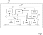
- FIG. 1 is a block diagram of an electronic device 100 comprising an integrated circuit 102 according to an embodiment of the present description.
- the electronic device 100 is for example a mobile electronic device, such as a mobile telephone, or an electronic card such as a microcircuit card.
- the circuit 102 comprises for example a processor 104 (CPU) connected to a non-volatile memory 106 (NV MEM) and to a volatile memory 108 (RAM) via a system bus 110.
- processor 104 CPU
- NV MEM non-volatile memory
- RAM volatile memory
- the memory 106 is a Flash type memory
- the memory 108 is a RAM type memory (from the English "Random Access Memory").
- the circuit 102 further comprises an interface circuit 112 (CCB - from the English "Coupling and Chaining Bridge") connected to the bus 110 via a bus 114.
- the term “coupling” refers to one or more transactions carried out in parallel by two peripheral circuits while the term “chaining” refers to one or more transactions performed in series by two peripheral circuits. In other words, in a chaining operation, the two peripheral circuits involved are occupied one after the other.
- the interface circuit is for example configured to provide a connection between the bus 114 and peripheral circuits.
- the interface circuit 112 will also be called here “coupling and chaining circuit", because it is capable of performing coupling and/or chaining functions in relation to the peripheral circuits.
- the bus 114 is for example an AHB type bus (from the English “Advanced High-performance Bus”). In other examples, the bus 114 is an APB type bus (from the English “Advanced Peripheral Bus”) or AXI type bus (from the English “Advanced External Interface”).
- the circuit 102 comprises, for example, peripheral circuits 116, 118, 120 and/or 122.
- the circuit 116 is for example a cryptographic circuit.
- the cryptographic circuit 116 is for example configured to encrypt and/or decrypt data according to a symmetric encryption algorithm, such as for example an algorithm of the AES type (from the English “Advanced Encryption Standard”).
- the circuit 118 is for example another cryptographic circuit.
- the circuit 118 is a circuit configured to perform hashing operations, for example according to an algorithm of the SHA type (from the English "Secure Digest Algorithm”).
- the cryptographic circuit 118 is further configured to perform cryptographic operations, such as for example, symmetric key generation and/or key derivation functions and/or shared key calculations, for example used for ECDH encryption and decryption (from the English "Elliptic Curve Diffie Hellman").
- the cryptographic circuit 118 is configured to generate SHA1, SHA2 and/or SHA3 type signatures or keyed hash message authentication codes (HMAC - the English “hashed MAC”).
- the circuit 120 is, for example, a true random number generator (TRNG) using a physical source of randomness based, for example, on intrinsic properties of the material on which it is implemented.
- the number generator is a pseudo-random number generator, for example a linear congruential generator.
- the number generator 120 is implemented in software, such as software stored and executed in the coupling and chaining circuit 112 if the latter includes a suitable processor and memory.
- the circuit 102 is configured so that the processor 104 does not have access to the values generated by the number generator 120 for a peripheral circuit among the circuits 116, 118 or 122.
- the circuit 122 is for example a key accelerator.
- the circuit 122 is configured to perform pre-calculations on a private or public key before it is for example processed by the cryptographic circuit 116 or by the cryptographic circuit 118.
- the processor 104 is for example a generic and non-secure processor. Thus, when sensitive data of the circuit 102, such as cryptographic keys stored in the non-volatile memory 106, are manipulated by the processor 104, their integrity is not guaranteed.
- the cryptographic circuits 116 and 118 and the circuit 122 are each connected, via a dedicated bus, to the coupling and chaining circuit 112.
- the number generator 120 is a hardware circuit
- the latter is also connected, for example, to the coupling and chaining circuit 112 via a dedicated bus.
- the coupling and chaining circuit 112 is configured to perform chaining operations on data exchanged between the circuits 116 to 122.
- peripheral circuits e.g. other cryptographic circuits
- other peripheral circuits are also connected to the coupling and chaining circuit 112 and in other embodiments, one or more of the circuits 116, 118, 120 and/or 122 could be omitted.
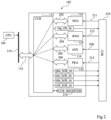
- FIG. 2 illustrates in more detail the circuit 102 according to an embodiment of the present description.
- the circuits 116, 118, 120 and 122 are, for example, each respectively connected to the coupling and chaining circuit 112 via a bus 200, 202, 204 and 206.
- the buses 110, 114 and 200 to 206 are AHB type buses.
- the buses 110, 114 and 200 to 206 are APB or AXI type buses.
- the buses 110, 114 and 200 to 206 are proprietary buses.
- the coupling and chaining circuit 112 is connected to other peripheral circuits (not shown) via dedicated buses.
- the coupling and chaining circuit 112 is connected to a cyclic redundancy check circuit configured to generate error checking codes based on data values.
- circuit 102 further includes a reset and clock control circuit (RCC) 210.
- RRC reset and clock control circuit
- circuit 210 is configured to control the timing of circuit 116, 118, 120, and 122, respectively, via clock buses 208, 211, 212, and 214, respectively.
- the coupling and chaining circuit 112 is further configured to control activation of one or more peripheral circuits 116, 118, and/or 122 via the clock reset circuit 210.
- the coupling and chaining circuit 112 transmits one or more activation signals aes_hclk_en, sha_hclk_en, pka_hclk_en, ccb_hclk_en, and/or rng_hclk_en to the clock reset circuit 210 to force the clock reset circuit 210 to clock the circuits 116, 118, 122, 112, and/or 120.
- the clock reset circuit 210 When the clock reset circuit 210 is forced to clock the circuits 116, 118, and/or 120, the clock reset circuit 210 transmits one or more activation signals aes_hclk_en, sha_hclk_en, pka_hclk_en, ccb_hclk_en, and/or rng_hclk_en to the clock reset circuit 210. 122, it is no longer possible to deactivate the clocking in software, for example by programming in registers of the circuit 210.
- the coupling and chaining circuit 112 is therefore capable of activating one or more of the circuits 116, 118, 120 and 122.
- the coupling and chaining circuit 112 is configured to perform read and/or write operations between the peripheral circuits 116, 118, 120 and/or 122 following the reception of an access request, to one of the peripheral circuits 116, 118, 120 and/or 122 and coming from the processor 104.
- the coupling and chaining circuit 112 includes a register 216 (CCB REGISTER) configured to store a state parameter.
- the state value conditions the behavior of the coupling and chaining circuit.
- the state value is for example programmed by the coupling and chaining circuit 112, and in particular by a state machine produced by the coupling and chaining circuit 112.
- the value of the state parameter written in the register 216 imposes a type of operation, for example a read and/or write operation, in the circuit 122.
- the value of the state parameter imposes, for example in addition, a sequence of states in the state machine, each state of the state machine being associated with one or more chaining and/or coupling operations between at least two peripheral circuits.
- a configuration value is for example stored in a register of the state machine. This value corresponds for example to a configuration of the coupling and chaining circuit 112, and for each configuration value, the value of the state parameter indicates to the coupling and chaining circuit 112 an operation to be performed.
- the same value of the state parameter signifies for example two different transactions.
- the possible sequences of the values taken by the state parameter differ depending on the value of the configuration parameter.
- FIG. 3 is a block diagram illustrating an example of operation implemented by the coupling and chaining circuit 112, between the circuits 120 and 122.
- the figure 3 illustrates a chaining operation, implemented by the coupling and chaining circuit 112. This operation is for example carried out for a first configuration value of the state machine.
- the value of the state parameter evolves. For example, the value of the state parameter is incremented following each transaction between two circuits.
- the processor 104 transmits a write data of a private key, or more generally a data value, to a destination address in the circuit 122.
- the coupling and chaining circuit 112 is configured to intercept the data value, transmitted via the bus 114.
- the coupling and chaining circuit 112 is further configured to, upon receipt of the write access request, command the generation of a value by the number generator 120. For example, before, or directly following, the transmission of the data value to be written by the processor, it is verified that a random value is available in the number generator circuit 120. For example, if no data is available in the number generator circuit 120, an error signal is generated. For example, following the generation of the error signal, all the data stored in the circuits 116, 118 and 122 are erased. Additionally, as an example, upon generation of the error signal, the write access request is aborted. In another example, for one or more given configuration values, processor 104 is permitted to write a value, known to processor 104, to circuit 122.
- the coupling and chaining circuit 112 is then configured to generate a new write request to the circuit 122 upon receipt of an access request for writing, in a volatile memory of the circuit 122, coming from the processor 104.
- the writing in the circuit 122 controlled by the circuit coupling and chaining 122 is for example carried out at the destination address indicated in the access request for writing by the processor 104.
- the processor 104 For example, whatever the value of the key, or more generally of the data, transmitted by the processor 104, it is a value generated by the number generator 120 which is written to the desired destination address in the circuit 122.
- the coupling and chaining circuit 112 is further configured to prohibit reading in the circuit 122 to the processor 104.
- the coupling and chaining circuit 112 is configured to return to the processor 104 a default value in response to an access request, coming from the processor 104, for reading and/or writing in the circuit 122.
- the value stored in a volatile memory of the circuit 122 instead of the data value transmitted by the processor 104, is inaccessible by the processor 104.
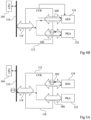
- FIG. 4A is a block diagram illustrating an example of an operation implemented by the coupling and chaining circuit 112 between the circuits 122 and 116. More particularly, the Figure 4A illustrates a chaining operation from circuit 122 to cryptographic circuit 116.
- the Figure 4A illustrates a chaining operation, implemented by the coupling and chaining circuit 112. This operation is for example carried out for a second configuration value of the state machine.
- the value of the state parameter evolves. For example, the value of the state parameter is incremented following each transaction between two circuits.
- the processor 104 wishes to access the circuit 122.
- the processor 104 transmits for example an access request for writing data stored at a destination address in the circuit 122.
- the coupling and chaining circuit 112 is configured to provide a default value to the processor 104 in response to a write access request, coming from the processor 104.
- the default value consists of indicating to the processor that the writing has been carried out, for example by returning a write done value.
- the coupling and chaining circuit 112 is further configured to, in response to the request for access to the destination address in the circuit 122, generate an access request for writing the data value stored at the destination address in the circuit 122, to the cryptographic circuit 116.
- the coupling and chaining circuit 112 is further configured for example to transform the write request from the processor 104 into a read request at the address given by the processor 104 in the volatile memory of the circuit 122 using a dedicated bus.
- the value retrieved from the volatile memory of the circuit 122 is then written, by the coupling and chaining circuit 112, in the circuit 116 at a fixed address which corresponds, for example, to the input of a FIFO (First Input First Output) type memory.
- a problem such as a write in the wrong format, for example a write of 1 byte or 2 bytes instead of a write of 4 bytes, an error is returned to the processor 104 in response to the write request.
- the cryptographic circuit 116 is then configured to encrypt the data value, for example according to a AES encryption algorithm.
- the encrypted value is accessible by the processor 104.
- the value of the data transmitted by the processor 104 is, for example, an additional parameter to the operation performed.
- the value of the data indicates an address in the circuit 116 to which the data, stored at the destination address in the circuit 122, is to be written.
- the coupling and chaining circuit 112 is configured to perform the operation described in connection with the Figure 4A only when the data value transmitted by the processor 104 is equal to a value defined upstream, such as for example a so-called magic value.
- the coupling and chaining circuit 112 upon receipt of an access request for writing a data value, is configured to compare the data value with a value for example stored in a register of the coupling and chaining circuit 112. For example, the comparison is performed by a state machine.
- the coupling and chaining circuit 112 is configured to, for example, perform an operation such as writing 0 in the volatile memory of the circuit 122.
- the writing of 0, by the processor 104 causes, for example, the stopping of the chaining operations, indicates to the circuit 122 the end of the transfer and allows the transition to the next configuration value for the state machine.
- FIG. 4B is a block diagram illustrating an example of an operation implemented by the coupling and chaining circuit 112 between the circuits 122 and 116. More particularly, the Figure 4B illustrates a chaining operation from circuit 116 to cryptographic circuit 122. This operation is for example carried out for a third configuration value of the state machine. In particular, During the execution of the described operation, the value of the state parameter changes. For example, the value of the state parameter is incremented following each transaction between two circuits.
- the processor 104 transmits for example an access request for writing to a destination address in the circuit 122.
- the chaining operation is performed when the data value transmitted by the processor 104 is equal to a value defined upstream, for example a magic value, for example equal to OxCCB.
- the coupling and chaining circuit 112 is configured to allow the writing of 0 in the volatile memory of the circuit 122 and to indicate the end of the writing in the volatile memory of the circuit 122 and the transition to the next configuration value for the state machine.
- the end of the writing in the volatile memory of the circuit 122 therefore results in the reprogramming of the configuration value.
- the comparison operation between the magic value and the data transmitted by the processor 104 is performed for a given value of the state parameter.
- the coupling and chaining circuit 112 is for example configured to, for example, control the decryption of the value stored at the destination address in the circuit 116, and its writing in the circuit 122.
- the value of the data to be written provided by the processor 104 indicates an address in the circuit 122 to which the decrypted value is to be written.
- the value of the data to be written transmitted by the processor 104 allows the coupling and chaining circuit 112 to determine between which peripheral circuits the operation is to be carried out.
- FIG. 5A is a block diagram illustrating an example of an operation implemented by the coupling and chaining circuit 112. More particularly, the operation illustrated in relation to the Figure 5A is performed between the circuit 122 and the cryptographic circuit 118. This operation is for example performed for a fourth configuration value of the state machine. In particular, during the performance of the operation described, the value of the state parameter changes. For example, the value of the state parameter is incremented following each transaction between two circuits.
- the coupling and chaining circuit 112 Upon receipt of an access request for writing a data value to a destination address in the circuit 122, the coupling and chaining circuit 112 is for example configured to command the writing of the data already stored at the destination address in the circuit 122 to the circuit 118.
- the value of the data transmitted by the processor 104 corresponds to an address in the circuit 118 to which the data is to be written. In another example, the value of the data to be written does not provide any information and a single address in the circuit 118 is accessible for writing.
- the data value transmitted by the processor 104 indicates, for example, between which peripheral devices the operation is to be performed.
- the circuit 118 is configured to perform cryptographic signature operations such as SHA2 or HMAC cryptographic operations, such as for example key derivation operations.
- the coupling and chaining circuit 112 is further configured to, in response to the access request transmitted by the processor 104, transmit a default value to the processor 104. The processor 104 then does not have access to the values stored in the circuits 118 and 122.
- FIG. 5B is a block diagram illustrating an example of an operation between the cryptographic circuits 116 and 118, implemented by the coupling and chaining circuit 112. This operation is for example carried out for a fifth configuration value of the state machine.
- the value of the state parameter evolves. For example, the value of the state parameter is incremented following each transaction between two circuits.
- Programming the configuration value to a value different from that described in relation to the Figure 4A allows for example the state machine to be placed in a state allowing chaining operations from circuit 118 to circuit 116 and no longer from circuit 122 to circuit 118.
- the operation described in relation to the Figure 5B is performed when the state parameter is programmed to the second state value.
- it is the value of the data transmitted by the processor 104 which allows for example the coupling and chaining circuit 112 to distinguish whether the operation to be performed is that described by the Figure 4A or that described in relation to the Figure 5B .
- the value of the data to be written determines whether the operation to be performed involves circuit 122 or circuit 118.
- the processor 104 sends an access request for writing to a destination address in the cryptographic circuit 118.
- the processor 104 requests access to the result previously generated by the circuit 118 following the operation described in relation to the Figure 5A .
- the coupling and chaining circuit 112 is for example configured to intercept the write access request and to command the writing of the data, already stored at the destination address in the circuit 118, to the circuit 116.
- the data value transmitted by the processor 104 corresponds to an address in the circuit 116 to which the data of the circuit 118 is to be written.
- the circuit 116 is configured to encrypt the data.
- the processor 104 then has, for example, access to the data value encrypted by the circuit 116.
- the coupling and chaining circuit 112 is configured to return a default value in response to the access request from the processor 104.
- the operations described in relation to the Figures 3, 4A , 4B, 5A And 5B are performed following a write access request from the processor 104, it is entirely possible to configure the coupling and chaining circuit 112 so that these operations are performed following read access requests.
- the coupling and chaining circuit 112 is configured to never authorize access by the processor 104 to data stored in one of the peripheral circuits 118, 120 and 122. For example, only data encrypted by the peripheral circuit 116 are accessible by the processor 104.
- the coupling circuit 112 is configured to control a read operation in the first circuit or in another circuit and to control the writing in the first circuit or in the other circuit
- the coupling circuit controls only read operations, or write operations, towards one and/or the other of the first and the other circuit.
- the type of operations controlled by the coupling circuit 112 is determined by the value of the state parameter and, for example, by the type of access requested by the processor 104.
- the direction of the data to be written depends on the value of the state parameter.
- the above examples are given for illustrative purposes and are not limiting.
- the address in the second circuit is a constant when the processor 104 addresses a first in first out (FIFO) type memory.
- the command for writing data, by the processor 104 is not relevant for defining the address in the second circuit.
- the command for writing data by the processor 104, is used to define a new type of operation when the data is moved between two circuits among the circuits 116, 118, 120 or 122.
- the new operation is a type of data exchange at the byte level, respectively at the bit level.
- part of the value of the data commanded for writing by the processor 104 is used to define an address in the second circuit and another part of the value is used to define the type of data exchange.
- the coupling and chaining circuit 112 is configured to intercept a transaction created by an initiator such as the processor 104 or such as a direct access memory (DMA) circuit in order to create new transactions between two peripheral circuits.
- an initiator such as the processor 104 or such as a direct access memory (DMA) circuit
- DMA direct access memory
- the nature of the new transaction depends, for example, on the value of the state parameter, the address and the data initiated.
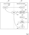
- FIG. 6 is a flowchart illustrating steps performed during different operating modes of the coupling and chaining circuit 112.
- a suspicious event refers to any unexpected transaction on the bus 114 and/or another bus.
- a suspicious event occurs during a physical attack on the circuit 102.
- Malware injected into the circuit 102 may also be the cause of a suspicious event.
- a suspicious event also occurs during a hardware attack or failure of the circuit 102.
- the coupling and chaining circuit 112 includes a state machine configured to detect the presence of a suspicious event to and/or in the coupling and chaining circuit 112.
- the state machine is configured to monitor transactions performed on the buses 114, 200, 202, 204, and 206.
- the state machine is configured to compare the data value with, for example, a list of authorized values. For example, when the data value does not match any of the data values included in the list, a suspicious event is detected.
- the list of authorized values includes several sublists, each sublist indicating authorized data values in association with a given state value.
- the configuration value is an initial value.
- the verification value is automatically programmed to the initial value.
- the coupling and chaining circuit 112 is then placed in a standard mode 601 (LEGACY MODE).
- the coupling and chaining circuit 112 is configured to act as a router.
- the state machine is for example deactivated.
- the coupling and chaining circuit 112 is configured to authorize and route the transactions, requested by the processor 104, to one or more peripheral circuits.
- the coupling and chaining circuit 112 acts as a router, the chaining or coupling operations are, for example, not executable.
- the coupling and chaining circuit 112 Upon receipt of an access request to a peripheral, the coupling and chaining circuit 112 then generates one or more transactions to only the peripheral circuit in question, and not to several peripherals.
- the standard mode is used for testing purposes.
- use cases of the circuit 102 are tested through particular data manipulations and associated tests and manipulations of non-secret values.
- the coupling and chaining circuit 112 is then placed in a protected mode 603 (PROTECTED MODE).
- the coupling and chaining circuit 112 is configured to, according to the value of the state parameter contained in the register 216 and/or the value of a data item transmitted for writing by the processor 104, perform one of the operations described in relation to the Figures 3, 4A , 4B, 5A and/or 5B.
- Step 602 further comprises, for example, access requests for writing keys in the circuit 122.
- the coupling and chaining circuit 112 is then configured to perform, for each request to write a key in the circuit 122, the operation described in relation to the figure 3 .
- step 602 consists of writing keys, generated by the number generator 120, it is entirely conceivable that other operations, for example having a purpose other than writing keys, are performed.
- the person skilled in the art will know how to adapt and configure the chaining and coupling circuit 112 to perform the desired operations between the desired peripheral circuits when the state parameter is programmed at the first state value.
- step 604 the state machine verifies that no suspicious event occurs.
- step 604 is performed in parallel with step 602.
- step 604 is performed following the writing of keys in circuit 12.
- the state machine verifies, for example, that the writing in the volatile memory of circuit 122 was carried out without error. For example, the state machine further verifies that the entire memory of circuit 122 is written.
- step 605 comprises reprogramming the configuration value to the initial value, returning the coupling and chaining circuit 112 to the standard state 601.
- step 605 further comprises deleting the content of the volatile memory of the circuit 122.
- step 605 further comprises deleting the content of memories internal to the peripheral circuits 116, 118, 120 and 122.
- step 605 further comprises erasing secret values, such as for example keys of encryption, stored in different registers of peripheral circuits 122, 116 and 118.
- step 604 If, when performing step 604, no suspicious event is detected by the state machine (branch Y), the method continues for example in a step 606 (OPSTEP ++). For example, when performing step 606, the state parameter is programmed, or incremented, to a new value.
- Step 606 further comprises, in response to a request for access for writing, or reading, from the processor 104, the execution of an operation among the operations for example described in relation to the Figures 4A , 4B, 5A and/or 5B.
- the nature of the operation and the peripheral circuits concerned depend on the value of the status parameter and the configuration value, and for example on the value of the data transmitted for writing.
- a step 607 (MORE ACTIONS?) is performed, for example by the state machine. For example, during step 607, the state machine determines whether other actions, for example depending on the configuration value, are to be performed. If this is the case (branch Y), the method resumes in a new implementation of step 604.
- the state machine configuration value determines the type of operation.
- the operation described in relation to the Figure 5A is performed before the operation described in relation to the Figure 5B .
- the operations performed are, in order, the operation described in relation to the Figure 5A , performing cryptographic operations such as a hashing operation by the circuit 118 and the operation described in connection with the Figure 5B .
- Step 608 takes place for example when the processor 104 no longer commands any access request to one or more of the peripheral circuits 116, 118, 120 and/or 122. Step 608 is then a final step in which the processor 104 has access for reading the results stored in the volatile memory of the circuit 122.
- step 608 the method ends in an embodiment of step 605, in which the value of the state parameter is reset and the contents of the internal memories of the circuits 116 to 122 are erased.
- the coupling and chaining circuit is then placed again in the standard mode.
- FIG. 7 is a table showing examples of different operations performed by the coupling and chaining circuit 112 depending on the value of the state parameter.
- a column 700 indicates for example the values that can be taken by the state parameter for a configuration value of the state machine.
- a sequence of values of the state parameter 0x6, 0x4, 0x8 and 0xA represents a succession of states of the state machine for a given configuration value.
- Step 606 then allows the transition from one state to the next state.
- the state parameter is for example accessible by the processor 104 in reading mode but is not accessible in writing mode by the processor 104.
- the circuit 102 in particular the coupling and chaining circuit 112, is configured to not authorize the processor 104 to modify the configuration value and the state value.
- the evolution of these values is for example internal to the coupling circuit. and chaining 112.
- the possible state sequences depend, for example, on the current configuration value.
- the value 0x0 indicates for example that the configuration value is programmed to the initial value and consequently that the circuit 112 is in the standard mode.
- the binary object when the value is less than 0x10, a binary object is being generated.
- the binary object comprises an encryption, for example by the circuit 116 and according to a Galois/Counter mode (GCM - "Galois Counter Mode") of the value provided by the number generator circuit 120.
- GCM Galois/Counter mode
- the binary object allows for example the provision of a reference value allowing for example to verify the integrity of the data handled during the transactions between the processor 104 and the circuits 122, 120, 118 and 116.
- the reference value is for example calculated according to the sequence of operations carried out.
- a column 702 indicates an operating mode of the circuit 122 depending on the value of the state parameter.
- the operating mode of the circuit 122 is defined by a value that can be equal to 0x24 or to N/A.
- the circuit 122 in the standard mode, the circuit 122 is automatically placed in an operating mode associated with the value N/A, indicating for example that the circuit 122 is operating normally or is inoperative.
- the value 0x24 indicates that access to the circuit 122 is controlled by the coupling and chaining circuit 112 and according to the configuration value.
- the value of the configuration parameter imposes the operating mode of the circuit 122.
- a column 704 indicates a mode of operation of circuit 116. For example, when the value of column 704 is equal to 0x2, circuit 116 is configured to encrypt, in a Galois/Counter mode, payload data. For example, when the value of column 704 is equal to 0x3, the binary object is completely generated and the reference value can be recovered, for example by the coupling and chaining circuit 112. The value N/A indicates that the circuit 116 is operating as expected in the standard mode.
- a column 706 indicates the type of operations, for example among the operations described in relation to the Figures 3, 4A , 4B, 5A and/or 5B, which is achievable, depending on the value of the state parameter.
- the coupling and chaining circuit 112 acts as a router.
- the operations described in relation to the Figures 3, 4A , 4B, 5A and 5C are not executable (N/A).
- N/A For example, when the value of the status parameter is 0x6, the possible operation is the one described in relation to the figure 3 (RNG->PKA).
- the possible operation is the one described in relation to the Figure 4A (PKA -> AES).
- the processor 104 when the state parameter is equal to 0xA or 0x4, no chaining and coupling operation is possible.
- the processor 104 then has, for example, when the value of the state parameter is equal to 0x4, the authorization to write in the circuit 122, but no operation, neither coupling nor chaining, will be carried out by the coupling and chaining circuit 112 in response to this writing.
- a column 708 indicates for example a parameterization of the coupling and chaining circuit 112 indicating the end of an operation. For example, each time a value indicating the end of an operation is stored, the state parameter is reprogrammed, or incremented, to a new value of the state parameter. The reprogramming, or incrementing the value of the state parameter, is for example executed by the state machine. In particular, the state machine is configured to reprogram or increment the value of the state parameter when a final condition is verified. As an example, the final condition corresponds to writing the value 0x3, for example in the circuit 116 and according to the example described in relation to the column 704. The writing of this value is for example triggered by the processor 104 or by another hardware circuit of the circuit 102.
- the processor 104 is not authorized to modify the state value.
- the processor 104 programs for example a value indicating the end of an operation. For example, the programming of this value by the processor 104 causes the coupling and chaining circuit 112 to return to standard mode.
- a column 710 (CPU ACTION) indicates for example the actions which can be carried out by the processor 104 depending on the value of the state parameter.
- the processor 104 can transmit write requests in the circuit 122 (WRITE IN PKA).
- Column 706 indicates that the operation described in relation to the figure 3 is performed.
- keys generated by the number generator circuit 120 are written to the volatile memory of the circuit 122.
- a RNGOKF SET value is stored when a predetermined number of keys has been written to the memory of the circuit 122.
- the RNGOKF SET value is stored when the memory of the circuit 122 is full.
- storing the RNGOKF SET value SET causes the state parameter to be programmed, or incremented, to the value 0x8.
- the state machine is for example configured to check the content of the volatile memory of the circuit 122. For example, the state machine checks that all of the data transmitted by the processor 104 has been written in the volatile memory of the circuit 122. For example, once the memory check has been successfully completed, a data value DATAOKF SET is stored in the coupling and chaining circuit 112.
- the processor 104 writes a private key to the circuit 122.
- the write sequence for the write operation depends on the value of the state parameter stored in the register 216.
- storing the DATAOKF SET value causes the state parameter value to be reprogrammed, or incremented, to the value 0x8.
- the processor 104 can, for example, transmit write and/or read requests to the circuit 122 (READ/WRITE IN PKA).
- Column 706 indicates that the operation performed by the coupling and chaining circuit 112 is then, for example, the operation described in relation to the Figure 4A .
- the processor 104 is configured to indicate to the coupling and chaining circuit 112 that the sequence of access requests for reading in the circuit 122 is complete. For example, this indication takes the form of an access request for writing a data value, the data value being known for example by the machine status and indicating that the read and/or write sequence is complete.
- the operating mode of circuit 116 is then also modified.
- the coupling and chaining circuit 112 is configured to receive access requests for reading data in the circuit 116 (READ IN AES) from the processor 104.
- the processor 104 also reads, in the peripheral circuit 116, the reference value generated via the binary object.
- the coupling and chaining circuit 112 is then configured to perform no operation (N/A).
- N/A no operation
- an IPRST value is for example stored in the coupling and chaining circuit 112.
- the storage of the IPRST value causes for example the reprogramming of the state parameter to the initial value.
- the peripheral circuits 116, 118 and 122 are reset (RESET).
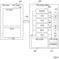
- FIG. 8 is a block diagram illustrating another embodiment of the electronic device 100.
- the circuit 102 comprises a secure area 800 (SECURED AREA) connected to a non-secure area 802 (APP. AND CPU AREA) via a bus 804.
- SECURED AREA secure area 800
- APP. AND CPU AREA non-secure area 802
- the secure area 800 comprises the circuits 116, 118, 120 and 122 as well as the coupling and chaining circuit 112.
- the circuit 122 is connected to a volatile memory 805 (PKA RAM) configured to store data transmitted by the coupling and chaining circuit 112.
- PKA RAM volatile memory 805
- the secure zone 800 further comprises, for example, another cryptographic circuit 806 (AES2), for example configured to encrypt and/or decrypt data according to a cryptographic algorithm, such as, for example, an AES type algorithm.
- AES2 another cryptographic circuit 806
- the secure zone 800 further comprises other peripheral circuits 808, such as for example a cyclic redundancy control circuit.
- the secure area 800 further comprises a dedicated processor 810 (CPU2) connected to the coupling and chaining circuit 112 via a bus.
- the area 800 for example further comprises a non-volatile, non-modifiable memory 812 (ROM, from the English “Read Only Memory”) as well as a volatile memory 814 (CPU RAM) and a non-volatile memory 816 (NV MEM2).
- the dedicated processor 802 is configured to perform the coupling and/or chaining operations via the coupling and chaining circuit 112. According to this embodiment, only the processor 810 is configured to perform secure operations, and consequently, to manipulate the generated binary objects.
- the non-secure area 802 includes the processor 104, as well as the non-volatile and volatile memories 106 and 108.
- An advantage of the described embodiments is that the processor 104 cannot read the plaintext data and does not cannot make a transaction with the coupling and chaining circuit 112.
- Another advantage of the described embodiments is that the dedicated processor 810, although able to use the coupling and chaining circuit 112, also cannot read cleartext data.
- the use of the processor 810 provides an additional level of isolation for sensitive data and secrets.
- peripheral circuits comprising the combination, at the system level, of the peripheral circuits with a chaining or coupling circuit, are that they allow to improve the performance in terms of processing time and/or to provide new functionalities without modifying the existing peripherals.
- the peripheral circuits such as for example a cryptographic circuit and a cyclic redundancy check circuit, or any other peripheral circuit, have the possibility of being used separately or in combination depending on the mode of use of the coupling and chaining circuit.
- Another advantage of the embodiments described is that they allow the processing of a data value by two peripheral circuits in parallel.
- the use of the coupling and chaining circuit allows the surface area of the circuit to be reduced.
- a chaining operation requires only a single data transfer request from the processor 104.
- the embodiments described allow the performance, in terms of processing time, of the device to be improved and reduce its energy consumption.
- Another advantage of the described embodiments is that, compared to using only the processor without coupling and chaining circuitry, fewer operations are required. necessary to perform a chaining or coupling operation between two devices. Indeed, a single access request from the processor allows the generation, by the coupling and chaining circuit, of other operations.
- peripheral circuits described are mainly cryptographic circuits, other types of circuits can be connected to the coupling and chaining circuit.
Landscapes
- Engineering & Computer Science (AREA)
- Theoretical Computer Science (AREA)
- Computer Security & Cryptography (AREA)
- Physics & Mathematics (AREA)
- General Engineering & Computer Science (AREA)
- General Physics & Mathematics (AREA)
- Computer Hardware Design (AREA)
- Software Systems (AREA)
- Computer Networks & Wireless Communication (AREA)
- Signal Processing (AREA)
- Mathematical Physics (AREA)
- Storage Device Security (AREA)
Applications Claiming Priority (1)
| Application Number | Priority Date | Filing Date | Title |
|---|---|---|---|
| FR2303154A FR3147398A1 (fr) | 2023-03-31 | 2023-03-31 | Circuit et procédé d’interface avec des circuits périphériques |
Publications (2)
| Publication Number | Publication Date |
|---|---|
| EP4439367A1 true EP4439367A1 (de) | 2024-10-02 |
| EP4439367B1 EP4439367B1 (de) | 2025-09-03 |
Family
ID=87571162
Family Applications (1)
| Application Number | Title | Priority Date | Filing Date |
|---|---|---|---|
| EP24164625.6A Active EP4439367B1 (de) | 2023-03-31 | 2024-03-19 | Schaltung und verfahren zur schnittstellenbildung mit peripherieschaltungen |
Country Status (3)
| Country | Link |
|---|---|
| US (1) | US20260037452A1 (de) |
| EP (1) | EP4439367B1 (de) |
| FR (1) | FR3147398A1 (de) |
Citations (3)
| Publication number | Priority date | Publication date | Assignee | Title |
|---|---|---|---|---|
| US6708273B1 (en) * | 1997-09-16 | 2004-03-16 | Safenet, Inc. | Apparatus and method for implementing IPSEC transforms within an integrated circuit |
| EP1870814A1 (de) * | 2006-06-19 | 2007-12-26 | Texas Instruments France | Verfahren, Vorrichtungen und Systeme für sicheren, nachfragebasierten Seitenabruf und andere Seitenabruf Vorgänge für Prozessorvorrichtungen |
| US20120008768A1 (en) * | 2010-07-08 | 2012-01-12 | Texas Instruments Incorporated | Mode control engine (mce) for confidentiality and other modes, circuits and processes |
-
2023
- 2023-03-31 FR FR2303154A patent/FR3147398A1/fr active Pending
-
2024
- 2024-03-19 EP EP24164625.6A patent/EP4439367B1/de active Active
- 2024-03-27 US US18/617,982 patent/US20260037452A1/en active Pending
Patent Citations (3)
| Publication number | Priority date | Publication date | Assignee | Title |
|---|---|---|---|---|
| US6708273B1 (en) * | 1997-09-16 | 2004-03-16 | Safenet, Inc. | Apparatus and method for implementing IPSEC transforms within an integrated circuit |
| EP1870814A1 (de) * | 2006-06-19 | 2007-12-26 | Texas Instruments France | Verfahren, Vorrichtungen und Systeme für sicheren, nachfragebasierten Seitenabruf und andere Seitenabruf Vorgänge für Prozessorvorrichtungen |
| US20120008768A1 (en) * | 2010-07-08 | 2012-01-12 | Texas Instruments Incorporated | Mode control engine (mce) for confidentiality and other modes, circuits and processes |
Also Published As
| Publication number | Publication date |
|---|---|
| FR3147398A1 (fr) | 2024-10-04 |
| EP4439367B1 (de) | 2025-09-03 |
| US20260037452A1 (en) | 2026-02-05 |
Similar Documents
| Publication | Publication Date | Title |
|---|---|---|
| US12079350B2 (en) | Secure public key acceleration | |
| EP2988243B1 (de) | Gerät und Verfahren um Dienste eines sicheren Plattformmoduls sicherzustellen | |
| US20090285390A1 (en) | Integrated circuit with secured software image and method therefor | |
| FR2995707A1 (fr) | Systemes et procedes de gestion de cles de chiffrement dans un microcontroleur securise | |
| US11847209B2 (en) | Memory device and system | |
| FR2984553A1 (fr) | Procede et dispositif de detection de fautes | |
| FR2979443A1 (fr) | Microcontroleur securise a base de mode | |
| EP1983436B1 (de) | Kontrolle der Integrität eines prozessorexternen Speichers | |
| KR20190038609A (ko) | 순서 검증 | |
| US12339959B2 (en) | Sparse encodings for control signals | |
| EP4068134B1 (de) | Gesicherte fehlerbeseitigung | |
| JP7770418B2 (ja) | 読み取り専用メモリ(rom)のセキュリティ | |
| CN113127262A (zh) | 镜像文件的生成方法、装置、电子设备及存储介质 | |
| EP4439367B1 (de) | Schaltung und verfahren zur schnittstellenbildung mit peripherieschaltungen | |
| EP3044721B1 (de) | Automatische paarung von io-vorrichtungen mit sicheren hardware-elementen | |
| JP7654819B2 (ja) | 読み取り専用メモリ(rom)のセキュリティ | |
| US20250211448A1 (en) | Storage device, operating method of controller, and system | |
| US11467954B2 (en) | Passing data between programs using read-once memory | |
| US20250038989A1 (en) | Securing access of storage array services | |
| CN112131612B (zh) | 一种cf卡数据防篡改方法、装置、设备及介质 | |
| EP4439315A1 (de) | Verfahren und schaltung zur emulation eines festwertspeichers | |
| CN118586003A (zh) | 一种基于国密算法的安全bootloader方法、装置及介质 | |
| CN119276452A (zh) | 同态加密算术设备及其操作方法 |
Legal Events
| Date | Code | Title | Description |
|---|---|---|---|
| PUAI | Public reference made under article 153(3) epc to a published international application that has entered the european phase |
Free format text: ORIGINAL CODE: 0009012 |
|
| STAA | Information on the status of an ep patent application or granted ep patent |
Free format text: STATUS: REQUEST FOR EXAMINATION WAS MADE |
|
| 17P | Request for examination filed |
Effective date: 20240319 |
|
| AK | Designated contracting states |
Kind code of ref document: A1 Designated state(s): AL AT BE BG CH CY CZ DE DK EE ES FI FR GB GR HR HU IE IS IT LI LT LU LV MC ME MK MT NL NO PL PT RO RS SE SI SK SM TR |
|
| REG | Reference to a national code |
Ref country code: DE Ref legal event code: R079 Free format text: PREVIOUS MAIN CLASS: G06F0021720000 Ipc: G06F0012140000 Ref country code: DE Ref legal event code: R079 Ref document number: 602024000567 Country of ref document: DE Free format text: PREVIOUS MAIN CLASS: G06F0021720000 Ipc: G06F0012140000 |
|
| GRAP | Despatch of communication of intention to grant a patent |
Free format text: ORIGINAL CODE: EPIDOSNIGR1 |
|
| STAA | Information on the status of an ep patent application or granted ep patent |
Free format text: STATUS: GRANT OF PATENT IS INTENDED |
|
| RIC1 | Information provided on ipc code assigned before grant |
Ipc: H04L 9/08 20060101ALI20250417BHEP Ipc: H04L 9/06 20060101ALI20250417BHEP Ipc: G06F 21/74 20130101ALI20250417BHEP Ipc: G06F 21/72 20130101ALI20250417BHEP Ipc: G06F 21/34 20130101ALI20250417BHEP Ipc: G06F 12/14 20060101AFI20250417BHEP |
|
| INTG | Intention to grant announced |
Effective date: 20250514 |
|
| GRAS | Grant fee paid |
Free format text: ORIGINAL CODE: EPIDOSNIGR3 |
|
| GRAA | (expected) grant |
Free format text: ORIGINAL CODE: 0009210 |
|
| STAA | Information on the status of an ep patent application or granted ep patent |
Free format text: STATUS: THE PATENT HAS BEEN GRANTED |
|
| AK | Designated contracting states |
Kind code of ref document: B1 Designated state(s): AL AT BE BG CH CY CZ DE DK EE ES FI FR GB GR HR HU IE IS IT LI LT LU LV MC ME MK MT NL NO PL PT RO RS SE SI SK SM TR |
|
| REG | Reference to a national code |
Ref country code: CH Ref legal event code: EP |
|
| REG | Reference to a national code |
Ref country code: DE Ref legal event code: R096 Ref document number: 602024000567 Country of ref document: DE |
|
| REG | Reference to a national code |
Ref country code: IE Ref legal event code: FG4D Free format text: LANGUAGE OF EP DOCUMENT: FRENCH |
|
| REG | Reference to a national code |
Ref country code: NL Ref legal event code: MP Effective date: 20250903 |
|
| PG25 | Lapsed in a contracting state [announced via postgrant information from national office to epo] |
Ref country code: NO Free format text: LAPSE BECAUSE OF FAILURE TO SUBMIT A TRANSLATION OF THE DESCRIPTION OR TO PAY THE FEE WITHIN THE PRESCRIBED TIME-LIMIT Effective date: 20251203 |
|
| REG | Reference to a national code |
Ref country code: LT Ref legal event code: MG9D |
|
| PG25 | Lapsed in a contracting state [announced via postgrant information from national office to epo] |
Ref country code: FI Free format text: LAPSE BECAUSE OF FAILURE TO SUBMIT A TRANSLATION OF THE DESCRIPTION OR TO PAY THE FEE WITHIN THE PRESCRIBED TIME-LIMIT Effective date: 20250903 |
|
| PG25 | Lapsed in a contracting state [announced via postgrant information from national office to epo] |
Ref country code: HR Free format text: LAPSE BECAUSE OF FAILURE TO SUBMIT A TRANSLATION OF THE DESCRIPTION OR TO PAY THE FEE WITHIN THE PRESCRIBED TIME-LIMIT Effective date: 20250903 |
|
| PG25 | Lapsed in a contracting state [announced via postgrant information from national office to epo] |
Ref country code: GR Free format text: LAPSE BECAUSE OF FAILURE TO SUBMIT A TRANSLATION OF THE DESCRIPTION OR TO PAY THE FEE WITHIN THE PRESCRIBED TIME-LIMIT Effective date: 20251204 |
|
| PG25 | Lapsed in a contracting state [announced via postgrant information from national office to epo] |
Ref country code: SE Free format text: LAPSE BECAUSE OF FAILURE TO SUBMIT A TRANSLATION OF THE DESCRIPTION OR TO PAY THE FEE WITHIN THE PRESCRIBED TIME-LIMIT Effective date: 20250903 |
|
| PG25 | Lapsed in a contracting state [announced via postgrant information from national office to epo] |
Ref country code: LV Free format text: LAPSE BECAUSE OF FAILURE TO SUBMIT A TRANSLATION OF THE DESCRIPTION OR TO PAY THE FEE WITHIN THE PRESCRIBED TIME-LIMIT Effective date: 20250903 |
|
| PG25 | Lapsed in a contracting state [announced via postgrant information from national office to epo] |
Ref country code: BG Free format text: LAPSE BECAUSE OF FAILURE TO SUBMIT A TRANSLATION OF THE DESCRIPTION OR TO PAY THE FEE WITHIN THE PRESCRIBED TIME-LIMIT Effective date: 20250903 Ref country code: PL Free format text: LAPSE BECAUSE OF FAILURE TO SUBMIT A TRANSLATION OF THE DESCRIPTION OR TO PAY THE FEE WITHIN THE PRESCRIBED TIME-LIMIT Effective date: 20250903 |
|
| PG25 | Lapsed in a contracting state [announced via postgrant information from national office to epo] |
Ref country code: RS Free format text: LAPSE BECAUSE OF FAILURE TO SUBMIT A TRANSLATION OF THE DESCRIPTION OR TO PAY THE FEE WITHIN THE PRESCRIBED TIME-LIMIT Effective date: 20251203 |
|
| PG25 | Lapsed in a contracting state [announced via postgrant information from national office to epo] |
Ref country code: ES Free format text: LAPSE BECAUSE OF FAILURE TO SUBMIT A TRANSLATION OF THE DESCRIPTION OR TO PAY THE FEE WITHIN THE PRESCRIBED TIME-LIMIT Effective date: 20250903 |
|
| REG | Reference to a national code |
Ref country code: AT Ref legal event code: MK05 Ref document number: 1833908 Country of ref document: AT Kind code of ref document: T Effective date: 20250903 |
|
| PG25 | Lapsed in a contracting state [announced via postgrant information from national office to epo] |
Ref country code: NL Free format text: LAPSE BECAUSE OF FAILURE TO SUBMIT A TRANSLATION OF THE DESCRIPTION OR TO PAY THE FEE WITHIN THE PRESCRIBED TIME-LIMIT Effective date: 20250903 |