EP4435832A1 - Organic light-emitting diode display panel and manufacturing method therefor - Google Patents
Organic light-emitting diode display panel and manufacturing method therefor Download PDFInfo
- Publication number
- EP4435832A1 EP4435832A1 EP21827379.5A EP21827379A EP4435832A1 EP 4435832 A1 EP4435832 A1 EP 4435832A1 EP 21827379 A EP21827379 A EP 21827379A EP 4435832 A1 EP4435832 A1 EP 4435832A1
- Authority
- EP
- European Patent Office
- Prior art keywords
- thin
- organic light
- display panel
- emitting diode
- diode display
- Prior art date
- Legal status (The legal status is an assumption and is not a legal conclusion. Google has not performed a legal analysis and makes no representation as to the accuracy of the status listed.)
- Pending
Links
Images



Classifications
-
- H—ELECTRICITY
- H10—SEMICONDUCTOR DEVICES; ELECTRIC SOLID-STATE DEVICES NOT OTHERWISE PROVIDED FOR
- H10K—ORGANIC ELECTRIC SOLID-STATE DEVICES
- H10K50/00—Organic light-emitting devices
- H10K50/80—Constructional details
- H10K50/805—Electrodes
-
- H—ELECTRICITY
- H10—SEMICONDUCTOR DEVICES; ELECTRIC SOLID-STATE DEVICES NOT OTHERWISE PROVIDED FOR
- H10K—ORGANIC ELECTRIC SOLID-STATE DEVICES
- H10K59/00—Integrated devices, or assemblies of multiple devices, comprising at least one organic light-emitting element covered by group H10K50/00
- H10K59/10—OLED displays
- H10K59/12—Active-matrix OLED [AMOLED] displays
- H10K59/1201—Manufacture or treatment
-
- H—ELECTRICITY
- H10—SEMICONDUCTOR DEVICES; ELECTRIC SOLID-STATE DEVICES NOT OTHERWISE PROVIDED FOR
- H10K—ORGANIC ELECTRIC SOLID-STATE DEVICES
- H10K59/00—Integrated devices, or assemblies of multiple devices, comprising at least one organic light-emitting element covered by group H10K50/00
- H10K59/10—OLED displays
- H10K59/12—Active-matrix OLED [AMOLED] displays
- H10K59/121—Active-matrix OLED [AMOLED] displays characterised by the geometry or disposition of pixel elements
- H10K59/1213—Active-matrix OLED [AMOLED] displays characterised by the geometry or disposition of pixel elements the pixel elements being TFTs
-
- H—ELECTRICITY
- H10—SEMICONDUCTOR DEVICES; ELECTRIC SOLID-STATE DEVICES NOT OTHERWISE PROVIDED FOR
- H10K—ORGANIC ELECTRIC SOLID-STATE DEVICES
- H10K59/00—Integrated devices, or assemblies of multiple devices, comprising at least one organic light-emitting element covered by group H10K50/00
- H10K59/10—OLED displays
- H10K59/12—Active-matrix OLED [AMOLED] displays
- H10K59/123—Connection of the pixel electrodes to the thin film transistors [TFT]
-
- H—ELECTRICITY
- H10—SEMICONDUCTOR DEVICES; ELECTRIC SOLID-STATE DEVICES NOT OTHERWISE PROVIDED FOR
- H10K—ORGANIC ELECTRIC SOLID-STATE DEVICES
- H10K59/00—Integrated devices, or assemblies of multiple devices, comprising at least one organic light-emitting element covered by group H10K50/00
- H10K59/10—OLED displays
- H10K59/12—Active-matrix OLED [AMOLED] displays
- H10K59/124—Insulating layers formed between TFT elements and OLED elements
-
- H—ELECTRICITY
- H10—SEMICONDUCTOR DEVICES; ELECTRIC SOLID-STATE DEVICES NOT OTHERWISE PROVIDED FOR
- H10K—ORGANIC ELECTRIC SOLID-STATE DEVICES
- H10K59/00—Integrated devices, or assemblies of multiple devices, comprising at least one organic light-emitting element covered by group H10K50/00
- H10K59/10—OLED displays
- H10K59/12—Active-matrix OLED [AMOLED] displays
- H10K59/126—Shielding, e.g. light-blocking means over the TFTs
-
- H—ELECTRICITY
- H10—SEMICONDUCTOR DEVICES; ELECTRIC SOLID-STATE DEVICES NOT OTHERWISE PROVIDED FOR
- H10K—ORGANIC ELECTRIC SOLID-STATE DEVICES
- H10K59/00—Integrated devices, or assemblies of multiple devices, comprising at least one organic light-emitting element covered by group H10K50/00
- H10K59/10—OLED displays
- H10K59/12—Active-matrix OLED [AMOLED] displays
- H10K59/131—Interconnections, e.g. wiring lines or terminals
-
- H—ELECTRICITY
- H10—SEMICONDUCTOR DEVICES; ELECTRIC SOLID-STATE DEVICES NOT OTHERWISE PROVIDED FOR
- H10K—ORGANIC ELECTRIC SOLID-STATE DEVICES
- H10K59/00—Integrated devices, or assemblies of multiple devices, comprising at least one organic light-emitting element covered by group H10K50/00
- H10K59/80—Constructional details
- H10K59/805—Electrodes
- H10K59/8051—Anodes
- H10K59/80515—Anodes characterised by their shape
-
- H—ELECTRICITY
- H10—SEMICONDUCTOR DEVICES; ELECTRIC SOLID-STATE DEVICES NOT OTHERWISE PROVIDED FOR
- H10K—ORGANIC ELECTRIC SOLID-STATE DEVICES
- H10K71/00—Manufacture or treatment specially adapted for the organic devices covered by this subclass
-
- H—ELECTRICITY
- H10—SEMICONDUCTOR DEVICES; ELECTRIC SOLID-STATE DEVICES NOT OTHERWISE PROVIDED FOR
- H10K—ORGANIC ELECTRIC SOLID-STATE DEVICES
- H10K71/00—Manufacture or treatment specially adapted for the organic devices covered by this subclass
- H10K71/80—Manufacture or treatment specially adapted for the organic devices covered by this subclass using temporary substrates
Definitions
- the present invention is related to the field of display technology and specifically to an organic light-emitting diode display panel and a manufacturing method thereof.
- Organic light-emitting diode display panels have advantages of wide viewing angles and wide color gamut. As mainstream display panels, they have been paid attention and developed by major display device manufacturers. Currently, the organic light-emitting diode display panels mostly use thin-film transistors with top gate structures, which are top-gate thin-film transistors. Compared with traditional thin-film transistors with bottom-gate structures, the top-gate thin-film transistors reduce manufacturing processes of the organic light-emitting diode display panels, thereby reducing manufacturing costs.
- a gate positioned in the middle of the top-gate thin-film transistor often causes a surface of the top-gate thin-film transistor to fluctuate, making a surface flatness of the top-gate thin-film transistor poor.
- the surface of the top-gate thin-film transistor is not flat enough, it will affect a light-emitting effect of a light-emitting layer on the top-gate thin-film transistor.
- a leveling layer is usually added onto the top-gate thin-film transistor.
- the leveling layer enables the light-emitting layer to be disposed on a flat surface of the leveling layer to increase the light-emitting effect of the light-emitting layer.
- the above-mentioned structure of the prior art can increase a display effect of the organic light-emitting diode display panel using the top-gate thin-film transistor, it also increases a thickness of the organic light-emitting diode display panel, increases manufacturing processes and manufacturing costs of the organic light-emitting diode display panel, and even affects flexibility of the organic light-emitting diode display panel.
- the traditional technology cannot take into account original advantages of the organic light-emitting diode display panel and solve technical problems of the top-gate thin-film transistor.
- the present invention provides an organic light-emitting diode display panel and a manufacturing method thereof, which can prevent problems faced by a traditional organic light-emitting diode display panel when using top-gate thin-film transistors. Meanwhile, the present invention can simplify manufacturing processes of the organic light-emitting diode display panel, enhance a light-emitting effect of the organic light-emitting diode display panel, and increase a pixel density of the organic light-emitting diode display panel, so as to enable viewers to obtain a better viewing effect.
- the organic light-emitting diode display panel of the present invention includes a thin-film transistor substrate, a plurality of thin-film transistors, and a plurality of organic light-emitting diodes.
- the thin-film transistors are disposed on a side of the thin-film transistor substrate.
- the organic light-emitting diodes are disposed on a side of the thin-film transistor substrate away from the thin-film transistors.
- each of the thin-film transistors includes a gate, a source, a drain, and a semiconductor layer.
- the semiconductor layer is electrically connected to the source and the drain.
- Each of the organic light-emitting diodes corresponds to each of the thin-film transistors and includes a first electrode, a light-emitting layer, and a second electrode.
- the first electrode is electrically connected to the source or the drain.
- the first electrode is disposed on the side of the thin-film transistor substrate away from the thin-film transistors.
- the light-emitting layer is disposed on a side of the first electrode away from the thin-film transistor substrate.
- the second electrode is disposed on a side of the light-emitting layer away from the first electrode.
- an area of the first electrode is greater than or equal to an area of the semiconductor layer.
- the first electrode blocks light from irradiating the semiconductor layer.
- a material of the first electrode includes an opaque material.
- the source and the drain are disposed on a side of the semiconductor layer away from the thin-film transistor substrate, and the gate is disposed on a side of the source and the drain away from the semiconductor layer.
- the gate is disposed on a side of the semiconductor layer away from the thin-film transistor substrate, and the source and the drain are disposed on a side of the gate away from the semiconductor layer.
- a total projected area of the gate, the source, and the drain on the semiconductor layer is greater than or equal to an area of the semiconductor layer.
- the gate, the source, and the drain block light from irradiating the semiconductor layer.
- the thin-film transistor substrate includes a through-hole, and the first electrode is electrically connected to the thin-film transistor through the through-hole.
- the organic light-emitting diode display panel further includes a peeling layer disposed between the thin-film transistor substrate and the organic light-emitting diodes.
- a material of the peeling layer includes gallium nitride.
- the manufacturing method of the organic light-emitting diode display panel of the present invention includes steps of:
- step S3 includes steps of:
- a total projected area of the gate, the source, and the drain on the semiconductor layer is greater than or equal to an area of the semiconductor layer.
- the gate, the source, and the drain block light from irradiating the semiconductor layer.
- step S36 includes steps of:
- step S4 includes a step of forming a first electrode on a side of the thin-film transistor substrate away from the thin-film transistors, forming a light-emitting layer on a side of the first electrode away from the thin-film transistor substrate, and forming a second electrode on a side of the light-emitting layer away from the first electrode.
- an area of the first electrode is greater than or equal to an area of the semiconductor layer.
- the first electrode blocks light from irradiating the semiconductor layer.
- a material of the first electrode includes an opaque material.
- step S1 includes a step of forming a peeling layer on a side of the first substrate.
- the manufacturing method further includes a step of separating the first substrate from the peeling layer.
- the peeling layer is separated from the first substrate by a laser ablation process.
- a material of the peeling layer includes gallium nitride.
- the organic light-emitting diode display panel and the manufacturing method of the organic light-emitting diode display panel of the present invention a traditional leveling layer and the organic light-emitting diodes are not disposed on the thin-film transistors.
- the organic light-emitting diodes are disposed on the side of the thin-film transistor substrate away from the thin-film transistors. Therefore, in the organic light-emitting diode display panel of the present invention, the organic light-emitting diodes are disposed on a flat surface and will not be affected by surface fluctuations caused by the gates of the thin-film transistors.
- the organic light-emitting diodes can be disposed on the flat surface, a space usage of the light-emitting layer can be maximized, thereby increasing a pixel density of the organic light-emitting diode display panel.
- the gate, the source, the drain, and the first electrode disposed on an upper side and a lower side of each of the thin-film transistors can also function as a light-shielding layer that blocks light for the semiconductor layer in each of the thin-film transistors.
- the invention provides an organic light-emitting diode display panel.
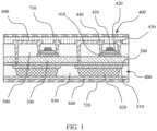
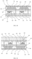
- FIG. 1 is a structural schematic diagram of the organic light-emitting diode display panel of the present invention.
- the organic light-emitting diode display panel includes a peeling layer 200, a thin-film transistor substrate 300, a plurality of thin-film transistors 400, and a plurality of organic light-emitting diodes 800.
- the peeling layer is made of semiconductor materials, including organic semiconductors or inorganic semiconductors.
- a material of the peeling layer 200 of the present invention includes gallium nitride (GaN) of an inorganic semiconductor.
- GaN gallium nitride
- the thin-film transistor substrate 300 is disposed on a side of the peeling layer 200, and the thin-film transistors 400 are disposed on a side of the thin-film transistor substrate 300 away from the peeling layer 200. Since the thin-film transistor substrate 300 insulates the peeling layer 200 from the thin-film transistors 400, it can be ensured that the peeling layer 200 will not directly contact the thin-film transistors 400, thereby preventing operations of the thin-film transistors 400 from affecting.
- Each of the thin-film transistors 400 serves as a driving switch for each of the organic light-emitting diodes 800, and includes a semiconductor layer 410, a gate insulating layer 420, a gate 430, a source 440, and a drain 450.
- the source 440 and the drain 450 are disposed on a side of the gate 430 away from the thin-film transistor substrate 300.
- each of the thin-film transistors 400 can control the on and off of a current at both ends of the source 440 and the drain 450.
- each of the thin-film transistors 400 of the present invention is not limited to the top-gate thin-film transistor, and may also be a bottom-gate thin-film transistor or a thin-film transistor having other structures.
- the gate 430 is disposed on a side of the semiconductor layer 410 away from the thin-film transistor substrate 300.
- the source 440 and the drain 450 are disposed on a side of the gate 430 away from the semiconductor layer 410.
- the semiconductor layer 410 is disposed between the thin-film transistor substrate 300 and the gate 430.
- the gate insulating layer 420 is disposed between the semiconductor layer 410 and the gate 430.
- the source 440 and the drain 450 are electrically connected to the semiconductor layer 410.
- the semiconductor layer 410 includes a metal oxide with a wide energy gap, so the semiconductor layer 410 of the present invention can construct a connection channel for the source 440 and the drain 450.
- the semiconductor layer 410 of the present invention includes indium gallium zinc oxide (IGZO).
- IGZO indium gallium zinc oxide
- An electron mobility of the indium gallium zinc oxide is 20-30 times that of a traditional amorphous silicon semiconductor, so a charge and discharge rate and response speed of each of the thin-film transistors 400 are significantly increased.
- Using the indium gallium zinc oxide as the channel of each of the thin-film transistors 400 can achieve a faster refresh rate of the organic light-emitting diode display panel.
- the indium gallium zinc oxide has a better driving capability, so driving power consumption of each of the thin-film transistors 400 is low, which makes the organic light-emitting diode display panel more energy-saving and power-saving, thereby greatly increasing a battery life of the organic light-emitting diode display panel.
- the organic light-emitting diode display panel further includes an interlayer dielectric layer 500.
- the interlayer dielectric layer 500 covers the semiconductor layer 410, the gate insulating layer 420, and the gate 430.
- the interlayer dielectric layer 500 has a high dielectric constant, which is used to insulate the gate 430 from the source 440 and the drain 450.
- the organic light-emitting diode display panel further includes a passivation layer 600 and a first encapsulation layer 710 sequentially disposed on a side of the thin-film transistors 400 away from the thin-film transistor substrate 300.
- the passivation layer 600 covers the source 440 and the drain 450 of each of the thin-film transistors 400, and further covers the interlayer dielectric layer 500.
- the passivation layer 600 not only has an insulating effect, but also imparts toughness to the organic light-emitting diode display panel when flexed.
- the first encapsulation layer 710 Through the arrangement of the first encapsulation layer 710, an outer side of the organic light-emitting diode display panel can be encapsulated to protect the organic light-emitting diode display panel.
- the organic light-emitting diodes 800 are disposed on a side of the thin-film transistor substrate 300 away from the thin-film transistors 400. Each of the organic light-emitting diodes 800 corresponds to each of the thin-film transistors 400. Each of the organic light-emitting diodes 800 includes a first electrode 810, a light-emitting layer 820, and a second electrode 840.
- the first electrode 810 is disposed on a side of the peeling layer 200 away from the thin-film transistor substrate 300.
- the first electrode 810 corresponds to each of the thin-film transistors 400.
- the light-emitting layer 820 can achieve the best space utilization efficiency and increase a pixel density of the organic light-emitting diode display panel.
- the source 440 of each of the thin-film transistors 400 is electrically connected to the first electrode 810.
- the drain 450 of each of the thin-film transistors 400 is electrically connected to the first electrode 810. Since the work performed by the source 440 or the drain 450 in each of the thin-film transistors 400 is only inputting or outputting a current, the present invention does not limit the source 440 or the drain 450 to be electrically connected to the first electrode 810.
- the light-emitting layer 820 is disposed on a side of the first electrode 810 away from the peeling layer 200.
- the light-emitting layer 820 is disposed on a surface of the first electrode 810 through an inkjet printing process.
- a pixel spacer 830 is filled between the light-emitting layers 820, so that the light-emitting layer 820 forms pixels of the organic light-emitting diode display panel.
- the second electrode 840 is disposed on a side of the light-emitting layer 820 away from the first electrode 810.
- the second electrode 840 covers the light-emitting layer 820 and the pixel spacer 830, and works as a common electrode with the first electrode 810 to drive the light-emitting layer 820 to emit light.
- the semiconductor layer 410 of each of the thin-film transistors 400 is sensitive to light. When light is irradiated on the semiconductor layer 410, a drift current effect is likely to occur and affect a driving effect of each of the thin-film transistors 400. Therefore, the traditional technology usually requires additional light-shielding layers to be provided on an upper side and a lower side of the semiconductor layer 410 of each of the thin-film transistors 400.
- the gate 430, the source 440, the drain 450, and the first electrode 810 can also provide a light shielding effect for the semiconductor layer 410, which can block light from irradiating the semiconductor layer 410.
- the gate 430, the source 440, and the drain 450 are disposed on a side of the semiconductor layer 410, and the first electrode 810 is disposed on a side of the semiconductor layer 410 away from the gate 430, the source 440, and the drain 450, the gate 430, the source 440, the drain 450, and the first electrode 810 can achieve the light-shielding effect of the light-shielding layer in the prior art, so the present invention can also simplify a structure of the organic light-emitting diode display panel.
- a total projected area of the gate 430, the source 440, and the drain 450 on the semiconductor layer 410 is greater than or equal to an area of the semiconductor layer 410.
- an area of the first electrode 810 is configured to be greater than or equal to an area of the semiconductor layer 410 of each of the thin-film transistors 400.
- a material of the first electrode 810 is an opaque conductive material, such as silver (Ag), indium tin oxide/silver/indium tin oxide (ITO/Ag/ITO) composite layer, indium zinc oxide/silver/ indium zinc oxide (IZO/Ag/IZO) composite layer, indium tin oxide/silver palladium copper alloy/indium tin oxide (ITO/APC/ITO) composite layer, or indium zinc oxide/silver palladium copper alloy/indium zinc oxide (IZO/APC/IZO) composite layer.
- silver silver
- ITO/Ag/ITO indium tin oxide/silver/indium tin oxide
- IZO/Ag/IZO indium zinc oxide/silver/ indium zinc oxide
- ITO/APC/ITO indium zinc oxide/silver palladium copper alloy/indium zinc oxide
- IZO/APC/IZO indium zinc oxide/silver palladium copper alloy/
- the organic light-emitting diode display panel of the present invention further includes a second encapsulation layer 720 disposed on a surface of the second electrode 840.
- a second encapsulation layer 720 disposed on a surface of the second electrode 840.
- the traditional leveling layer and the organic light-emitting diodes 800 are not disposed on the thin-film transistors 400.
- the organic light-emitting diodes 800 are disposed on the side of the thin-film transistor substrate 300 away from the thin-film transistors 400. Therefore, in the organic light-emitting diode display panel of the present invention, the organic light-emitting diodes 800 are disposed on a flat surface and will not be affected by surface fluctuations caused by the gates 430 of the thin-film transistors 400.
- the organic light-emitting diodes 800 can be disposed on the flat surface, a space usage of the light-emitting layer 820 can be maximized, thereby increasing the pixel density of the organic light-emitting diode display panel.
- the gate 430, the source 440, the drain 450, and the first electrode 810 disposed on an upper side and a lower side of each of the thin-film transistors 400 can also function as the light-shielding layer that blocks light for the semiconductor layer 410 in each of the thin-film transistors 400.
- the present invention further provides a manufacturing method of the above-mentioned organic light-emitting diode display panel.
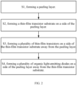
- FIG. 2 is a flowchart of steps S1-S4 of the manufacturing method of the organic light-emitting diode display panel of the present invention.
- the manufacturing method of the organic light-emitting diode display panel of the present invention shown in FIG. 1 mainly includes the following steps S1-S4.
- the peeling layer 200 is formed.
- the peeling layer is made of semiconductor materials, including organic semiconductors or inorganic semiconductors.
- a material of the peeling layer 200 of the present invention includes gallium nitride (GaN) of an inorganic semiconductor.
- step S1 includes forming the peeling layer 200 on a side of the first substrate 110.
- the first substrate 110 may be a glass substrate usually used in display panel industry, which provides a simple and convenient initial process for the manufacturing method of the organic light-emitting diode display panel of the present invention.
- a thin-film transistor substrate 300 is formed on a side of the peeling layer 200 away from the first substrate 110.
- the thin-film transistor substrate 300 insulates the peeling layer 200 from the thin-film transistors 400, it can be ensured that the peeling layer 200 will not directly contact the thin-film transistors 400 formed in subsequent step S3, thereby preventing operations of the thin-film transistors 400 from affecting.
- step S3 of FIG. 2 the thin-film transistors 400 shown in FIG. 1 are formed on the side of the thin-film transistor substrate 300 away from the peeling layer 200.
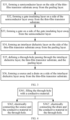
- step S3 includes the following steps S31-S36 to form each of the thin-film transistors 400 shown in FIG. 1 .
- the semiconductor layer 410 is formed on the side of the thin-film transistor substrate 300 away from the peeling layer 200 through a photolithography process.
- the semiconductor layer 410 includes a metal oxide with a wide energy gap, so the semiconductor layer 410 of the present invention can construct a connection channel for the source 440 and the drain 450 shown in FIG. 1 formed in step S36.
- the semiconductor layer 410 of the present invention includes indium gallium zinc oxide (IGZO).
- IGZO indium gallium zinc oxide
- An electron mobility of the indium gallium zinc oxide is 20-30 times that of a traditional amorphous silicon semiconductor, so a charge and discharge rate and response speed of each of the thin-film transistors 400 shown in FIG. 1 are significantly increased.
- the indium gallium zinc oxide as the channel of each of the thin-film transistors 400 can achieve a faster refresh rate of the organic light-emitting diode display panel. Meanwhile, the indium gallium zinc oxide has a better driving capability, so driving power consumption of each of the thin-film transistors 400 is low, which makes the organic light-emitting diode display panel more energy-saving and power-saving, thereby greatly increasing a battery life of the organic light-emitting diode display panel.
- the gate insulating layer 420 is formed on the side of the semiconductor layer 410 away from the thin-film transistor substrate 300 through the photolithography process. As shown in FIG. 1 , the gate insulating layer 420 is configured to insulate the semiconductor layer 410 from the gate 430 formed in subsequent step S33. In an embodiment, the gate insulating layer 420 is disposed on the semiconductor layer 410, and edges of the gate insulating layer 420 are retracted compared to edges of the semiconductor layer 410, which means that a lower surface area of the gate insulating layer 420 is smaller than an upper surface area of the semiconductor layer 410. The purpose is to reserve positions of the left and right sides of the semiconductor layer 410 to facilitate connections between the source 440 and the drain 450 formed in subsequent step S36.
- the gate 430 is formed on the side of the gate insulating layer 420 away from the semiconductor layer 410 through the photolithography process.
- the gate 430 is disposed on the gate insulating layer 420, and edges of the gate 430 is retracted compared to the edges of the gate insulating layer 420, which means that a lower surface area of the gate 430 is smaller than an upper surface area of the gate insulating layer 420.
- the purpose is to prevent the gate 430 from going beyond the edges of the gate insulating layer 420, and to retain positions of the left and right sides of the semiconductor layer 410 to facilitate connections between the source 440 and the drain 450 shown in FIG. 1 formed in subsequent step S36.
- the interlayer dielectric layer 500 is formed on the side of the thin-film transistor substrate 300 away from the peeling layer 200 through a coating process. After the interlayer dielectric layer 500 is coated on the thin-film transistor substrate 300, it will cover the semiconductor layer 410, the gate insulating layer 420, and the gate 430.
- the interlayer dielectric layer 500 has a high dielectric constant, which is configured to insulate the gate 430 from the source 440 and the drain 450 shown in FIG. 1 formed in subsequent step S36.
- step S35 the interlayer dielectric layer 500, the thin-film transistor substrate 300, and the peeling layer 200 are etched at different depths through a halftone mask, so as to form the through-holes 510 passing through the interlayer dielectric layer 500, the thin-film transistor substrate 300, and the peeling layer 200. Since the semiconductor layer 410, the gate insulating layer 420, and the gate 430 are covered by the interlayer dielectric layer 500, the source 440 and the drain 450 shown in FIG. 1 formed in subsequent step S36 cannot be electrically connected to the semiconductor layer 410. Therefore, when forming each of the thin-film transistors 400, it is necessary to form an electrical connection channel through an etching process.
- the through-holes 510 include a source through-hole 511 and a drain through-hole 512.
- the source through-hole 511 and the drain through-hole 512 pass through the interlayer dielectric layer 500 and expose the semiconductor layer 410.
- the through-holes 510 further include a first electrode through-hole 513.
- the first electrode through-hole 513 passes through the interlayer dielectric layer 500, the thin-film transistor substrate 300, and the peeling layer 200, and exposes the first substrate 110.
- step S36 the source 440 and the drain 450 are formed on the side of the interlayer dielectric layer 500 away from the thin-film transistor substrate 300 through the photolithography process.
- the thin-film transistors 400 formed in step S3 of the present invention are top-gate thin-film transistors.
- each of the thin-film transistors 400 serves as a driving switch for each of the organic light-emitting diodes 800, and includes the semiconductor layer 410, the gate insulating layer 420, the gate 430, the source 440, and the drain 450.
- each of the thin-film transistors 400 can control the on and off of a current at both ends of the source 440 and the drain 450.
- each of the thin-film transistors 400 of the present invention is not limited to the top-gate thin-film transistor, and may also be a bottom-gate thin-film transistor or a thin-film transistor having other structures.
- step S36 includes the following steps S361-S362/S362' to form the source 440 and the drain 450 shown in FIG. 1 .
- step S361 after the through-holes 510 are formed, the through-holes 510 will be filled with the conductive material.
- the source 440 and the drain 450 are formed on the through-holes 510, they are electrically connected to the conductive material in the through-holes 510. Therefore, in each of the thin-film transistors 400, the source 440 is electrically connected to the semiconductor layer 410 through the conductive material in the source through-hole 511, and the drain 450 is electrically connected to the semiconductor layer 410 through the drain through-hole 512.
- the conductive material is electrically connected to the semiconductor layer 410.
- the purpose of the first electrode through-hole 513 is to electrically connect the source 440 or the drain 450 of each of the thin-film transistors 400 to the first electrode 810 shown in FIG. 1 formed in subsequent step S4. Therefore, as shown in FIG. 12 , an embodiment of the present invention selects step S362, which means that the source 440 is electrically connected to the conductive material in the first electrode through-hole 513.
- step S362' may also be selected, so as to electrically connect the drain 450 to the conductive material in the first electrode through-hole 513.
- the present invention does not limit the source 440 or the drain 450 to be electrically connected to the first electrode 810 shown in FIG. 1 .
- a passivation layer 600 and a first encapsulation layer 710 are sequentially formed on a side of the thin-film transistors 400 away from the thin-film transistor substrate 300.
- the passivation layer 600 covers the source 440 and the drain 450 of each of the thin-film transistors 400, and further covers the interlayer dielectric layer 500.
- the passivation layer 600 not only has an insulating effect, but also imparts toughness to the organic light-emitting diode display panel when flexed.
- a semi-finished product of the organic light-emitting diode display panel formed in steps S1-S3 is attached to a second substrate 120 through the first encapsulation layer 710 to facilitate subsequent manufacturing processes.
- the manufacturing method of the organic light-emitting diode display panel of the present invention further includes separating the first substrate 110 from the peeling layer 200. Before the manufacturing method of the organic light-emitting diode display panel of the present invention proceeds to step S4, the first substrate 110 in a semi-finished product of the organic light-emitting diode display panel formed in the previous step is removed.
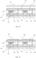
- FIG. 14 shows a semi-finished product of the organic light-emitting diode display panel turned upside down.
- the present invention flips the semi-finished organic light-emitting diode display panel in this manufacturing process, and uses a laser ablation process to peel the first substrate 110 from the peeling layer 200.
- a laser ablation process to peel the first substrate 110 from the peeling layer 200.
- FIG. 15 shows a semi-finished product of the organic light-emitting diode display panel turned upside down.
- the organic light-emitting diodes 800 are formed on the side of the peeling layer 200 away from the thin-film transistor substrate 300 through the photolithography process.
- Each of the organic light-emitting diodes 800 corresponds to each of the thin-film transistors 400.
- Each of the organic light-emitting diodes 800 includes the first electrode 810, a light-emitting layer 820, and a second electrode 840.
- the source 440 or the drain 450 of each of the thin-film transistors 400 are electrically connected to the first electrode 810.
- the light-emitting layer 820 shown in FIG. 1 can achieve the best space utilization efficiency and increase a pixel density of the organic light-emitting diode display panel.
- the semiconductor layer 410 of each of the thin-film transistors 400 is sensitive to light. When light is irradiated on the semiconductor layer 410, a drift current effect is likely to occur and affect a driving effect of each of the thin-film transistors 400. Therefore, the traditional technology usually requires additional light-shielding layers to be provided on an upper side and a lower side of the semiconductor layer 410 of each of the thin-film transistors 400.
- the gate 430, the source 440, the drain 450, and the first electrode 810 can also provide a light shielding effect for the semiconductor layer 410, which can block light from irradiating the semiconductor layer 410.
- the gate 430, the source 440, and the drain 450 are formed on a side of the semiconductor layer 410, and the first electrode 810 is formed on a side of the semiconductor layer 410 away from the gate 430, the source 440, and the drain 450, the gate 430, the source 440, the drain 450, and the first electrode 810 can achieve the light-shielding effect of the light-shielding layer in the prior art, so the present invention can also simplify a structure of the organic light-emitting diode display panel.
- a total projected area of the gate 430, the source 440, and the drain 450 on the semiconductor layer 410 is greater than or equal to an area of the semiconductor layer 410.
- an area of the first electrode 810 is configured to be greater than or equal to an area of the semiconductor layer 410 of each of the thin-film transistors 400.
- a material of the first electrode 810 is an opaque conductive material, such as silver (Ag), indium tin oxide/silver/indium tin oxide (ITO/Ag/ITO) composite layer, indium zinc oxide/silver/ indium zinc oxide (IZO/Ag/IZO) composite layer, indium tin oxide/silver palladium copper alloy/indium tin oxide (ITO/APC/ITO) composite layer, or indium zinc oxide/silver palladium copper alloy/indium zinc oxide (IZO/APC/IZO) composite layer.
- silver silver
- ITO/Ag/ITO indium tin oxide/silver/indium tin oxide
- IZO/Ag/IZO indium zinc oxide/silver/ indium zinc oxide
- ITO/APC/ITO indium zinc oxide/silver palladium copper alloy/indium zinc oxide
- IZO/APC/IZO indium zinc oxide/silver palladium copper alloy/
- FIG. 16 shows a semi-finished product of the organic light-emitting diode display panel turned upside down.
- the present invention forms the light-emitting layer 820 on a side of the first electrode 810 away from the peeling layer 200 through an inkjet printing process. Meanwhile, a pixel spacer 830 is filled between the light-emitting layers 820, so that the light-emitting layer 820 forms pixels of the organic light-emitting diode display panel.
- FIG. 17 shows a semi-finished product of the organic light-emitting diode display panel turned upside down.
- the second electrode 840 is formed on a side of the light-emitting layer 820 away from the first electrode 810.
- the second electrode 840 covers the light-emitting layer 820 and the pixel spacer 830, and works as a common electrode with the first electrode 810 to drive the light-emitting layer 820 to emit light.
- step S4 of FIG. 2 the present invention forms a second encapsulation layer 720 on a side of the second electrode 840 away from the light-emitting layer 820.
- the semi-finished product of the organic light-emitting diode display panel formed in steps S1-S4 is encapsulated by the second encapsulation layer 720 to protect the organic light-emitting diode display panel.
- the present invention separates the second substrate 120 from the first encapsulation layer 710 through the laser ablation process.
- the present invention flips the semi-finished organic light-emitting diode display panel again in this manufacturing process, and focuses the high-power nanosecond-femtosecond pulsed laser on the first encapsulation layer 710
- the first encapsulation layer 710 is irradiated by the laser it will generate gas, so that a bonding between the interfaces disappears.
- the second substrate 120 can be removed from the semi-finished product of the organic light-emitting diode display panel.
- the traditional leveling layer and the organic light-emitting diodes 800 are not formed on the thin-film transistors 400.
- the organic light-emitting diodes 800 are formed on the side of the thin-film transistor substrate 300 away from the thin-film transistors 400. Therefore, in the organic light-emitting diode display panel of the present invention, the organic light-emitting diodes 800 are formed on a flat surface and will not be affected by surface fluctuations caused by the gates 430 of the thin-film transistors 400.
- the organic light-emitting diodes 800 can be formed on the flat surface, a space usage of the light-emitting layer 820 can be maximized, thereby increasing the pixel density of the organic light-emitting diode display panel.
- the gate 430, the source 440, the drain 450, and the first electrode 810 formed on an upper side and a lower side of each of the thin-film transistors 400 can also function as the light-shielding layer that blocks light for the semiconductor layer 410 in each of the thin-film transistors 400.
Landscapes
- Engineering & Computer Science (AREA)
- Microelectronics & Electronic Packaging (AREA)
- Manufacturing & Machinery (AREA)
- Physics & Mathematics (AREA)
- Geometry (AREA)
- Optics & Photonics (AREA)
- Electroluminescent Light Sources (AREA)
- Devices For Indicating Variable Information By Combining Individual Elements (AREA)
- Thin Film Transistor (AREA)
Abstract
Description
- The present invention is related to the field of display technology and specifically to an organic light-emitting diode display panel and a manufacturing method thereof.
- Organic light-emitting diode display panels have advantages of wide viewing angles and wide color gamut. As mainstream display panels, they have been paid attention and developed by major display device manufacturers. Currently, the organic light-emitting diode display panels mostly use thin-film transistors with top gate structures, which are top-gate thin-film transistors. Compared with traditional thin-film transistors with bottom-gate structures, the top-gate thin-film transistors reduce manufacturing processes of the organic light-emitting diode display panels, thereby reducing manufacturing costs.
- However, in a top-gate thin-film transistor, a gate positioned in the middle of the top-gate thin-film transistor often causes a surface of the top-gate thin-film transistor to fluctuate, making a surface flatness of the top-gate thin-film transistor poor. When the surface of the top-gate thin-film transistor is not flat enough, it will affect a light-emitting effect of a light-emitting layer on the top-gate thin-film transistor.
- In the prior art, in order to increase the surface flatness of the top-gate thin-film transistor, a leveling layer is usually added onto the top-gate thin-film transistor. The leveling layer enables the light-emitting layer to be disposed on a flat surface of the leveling layer to increase the light-emitting effect of the light-emitting layer.
- Although the above-mentioned structure of the prior art can increase a display effect of the organic light-emitting diode display panel using the top-gate thin-film transistor, it also increases a thickness of the organic light-emitting diode display panel, increases manufacturing processes and manufacturing costs of the organic light-emitting diode display panel, and even affects flexibility of the organic light-emitting diode display panel.
- Therefore, the traditional technology cannot take into account original advantages of the organic light-emitting diode display panel and solve technical problems of the top-gate thin-film transistor.
- The present invention provides an organic light-emitting diode display panel and a manufacturing method thereof, which can prevent problems faced by a traditional organic light-emitting diode display panel when using top-gate thin-film transistors. Meanwhile, the present invention can simplify manufacturing processes of the organic light-emitting diode display panel, enhance a light-emitting effect of the organic light-emitting diode display panel, and increase a pixel density of the organic light-emitting diode display panel, so as to enable viewers to obtain a better viewing effect.
- The organic light-emitting diode display panel of the present invention includes a thin-film transistor substrate, a plurality of thin-film transistors, and a plurality of organic light-emitting diodes. The thin-film transistors are disposed on a side of the thin-film transistor substrate. The organic light-emitting diodes are disposed on a side of the thin-film transistor substrate away from the thin-film transistors.
- In an embodiment, each of the thin-film transistors includes a gate, a source, a drain, and a semiconductor layer. The semiconductor layer is electrically connected to the source and the drain. Each of the organic light-emitting diodes corresponds to each of the thin-film transistors and includes a first electrode, a light-emitting layer, and a second electrode. The first electrode is electrically connected to the source or the drain. The first electrode is disposed on the side of the thin-film transistor substrate away from the thin-film transistors. The light-emitting layer is disposed on a side of the first electrode away from the thin-film transistor substrate. The second electrode is disposed on a side of the light-emitting layer away from the first electrode.
- In an embodiment, an area of the first electrode is greater than or equal to an area of the semiconductor layer. The first electrode blocks light from irradiating the semiconductor layer.
- In an embodiment, a material of the first electrode includes an opaque material.
- In an embodiment, the source and the drain are disposed on a side of the semiconductor layer away from the thin-film transistor substrate, and the gate is disposed on a side of the source and the drain away from the semiconductor layer.
- In an embodiment, the gate is disposed on a side of the semiconductor layer away from the thin-film transistor substrate, and the source and the drain are disposed on a side of the gate away from the semiconductor layer.
- In an embodiment, a total projected area of the gate, the source, and the drain on the semiconductor layer is greater than or equal to an area of the semiconductor layer. The gate, the source, and the drain block light from irradiating the semiconductor layer.
- In an embodiment, the thin-film transistor substrate includes a through-hole, and the first electrode is electrically connected to the thin-film transistor through the through-hole.
- In an embodiment, the organic light-emitting diode display panel further includes a peeling layer disposed between the thin-film transistor substrate and the organic light-emitting diodes.
- In an embodiment, a material of the peeling layer includes gallium nitride.
- The manufacturing method of the organic light-emitting diode display panel of the present invention includes steps of:
- S 1, forming a peeling layer;
- S2, forming a thin-film transistor substrate on a side of the peeling layer;
- S3, forming a plurality of thin-film transistors on a side of the thin-film transistor substrate away from the peeling layer; and
- S4, forming a plurality of organic light-emitting diodes on a side of the peeling layer away from the thin-film transistor substrate.
- In an embodiment, step S3 includes steps of:
- S31, forming a semiconductor layer on the side of the thin-film transistor substrate away from the peeling layer;
- S32, forming a gate insulating layer on a side of the semiconductor layer away from the thin-film transistor substrate;
- S33, forming a gate on a side of the gate insulating layer away from the semiconductor layer;
- S34, forming an interlayer dielectric layer on the side of the thin-film transistor substrate away from the peeling layer;
- S35, defining a through-hole passing through the interlayer dielectric layer, the thin-film transistor substrate, and the peeling layer; and
- S36, forming a source and a drain on a side of the interlayer dielectric layer away from the thin-film transistor substrate.
- In an embodiment, a total projected area of the gate, the source, and the drain on the semiconductor layer is greater than or equal to an area of the semiconductor layer. The gate, the source, and the drain block light from irradiating the semiconductor layer.
- In an embodiment, step S36 includes steps of:
- S361, filling the through-hole with a conductive material;
- S362, electrically connecting the source and the conductive material in the through-hole; or
- S362', electrically connecting the drain and the conductive material in the through-hole.
- In an embodiment, step S4 includes a step of forming a first electrode on a side of the thin-film transistor substrate away from the thin-film transistors, forming a light-emitting layer on a side of the first electrode away from the thin-film transistor substrate, and forming a second electrode on a side of the light-emitting layer away from the first electrode.
- In an embodiment, an area of the first electrode is greater than or equal to an area of the semiconductor layer. The first electrode blocks light from irradiating the semiconductor layer.
- In an embodiment, a material of the first electrode includes an opaque material.
- In an embodiment, step S1 includes a step of forming a peeling layer on a side of the first substrate. Before step S4, the manufacturing method further includes a step of separating the first substrate from the peeling layer.
- In an embodiment, the peeling layer is separated from the first substrate by a laser ablation process.
- In an embodiment, a material of the peeling layer includes gallium nitride.
- In the organic light-emitting diode display panel and the manufacturing method of the organic light-emitting diode display panel of the present invention, a traditional leveling layer and the organic light-emitting diodes are not disposed on the thin-film transistors. On the contrary, the organic light-emitting diodes are disposed on the side of the thin-film transistor substrate away from the thin-film transistors. Therefore, in the organic light-emitting diode display panel of the present invention, the organic light-emitting diodes are disposed on a flat surface and will not be affected by surface fluctuations caused by the gates of the thin-film transistors. Since the organic light-emitting diodes can be disposed on the flat surface, a space usage of the light-emitting layer can be maximized, thereby increasing a pixel density of the organic light-emitting diode display panel. Meanwhile, the gate, the source, the drain, and the first electrode disposed on an upper side and a lower side of each of the thin-film transistors can also function as a light-shielding layer that blocks light for the semiconductor layer in each of the thin-film transistors. This can simplify manufacturing processes of the organic light-emitting diode display panel, increase a display efficiency of the thin-film transistors, and enhance a light-emitting effect of the organic light-emitting diode display panel, so as to enable viewers to obtain a better viewing effect.
-
-
FIG. 1 is a structural schematic diagram of an organic light-emitting diode display panel of the present invention. -
FIG. 2 is a flowchart of steps S1-S4 of a manufacturing method of the organic light-emitting diode display panel of the present invention. -
FIG. 3 is a flowchart of steps S31-S36 of the manufacturing method of the organic light-emitting diode display panel of the present invention. -
FIG. 4 is a flowchart of steps S361-S362/S362' of the manufacturing method of the organic light-emitting diode display panel of the present invention. -
FIGs. 5-19 are structural schematic diagrams showing the organic light-emitting diode display panel of the present invention at different manufacturing processes. - In order to make the above purposes, features, and advantages of the present invention more obvious and understandable, the following is a detailed description of preferred embodiments of the present invention in conjunction with accompanying drawings.
- The invention provides an organic light-emitting diode display panel. Please refer to
FIG. 1 , which is a structural schematic diagram of the organic light-emitting diode display panel of the present invention. The organic light-emitting diode display panel includes apeeling layer 200, a thin-film transistor substrate 300, a plurality of thin-film transistors 400, and a plurality of organic light-emittingdiodes 800. - The peeling layer is made of semiconductor materials, including organic semiconductors or inorganic semiconductors. In an embodiment, a material of the
peeling layer 200 of the present invention includes gallium nitride (GaN) of an inorganic semiconductor. When thepeeling layer 200 made of gallium nitride is irradiated by a laser, it will generate gas, which can separate components connected on its surface. Applications of thepeeling layer 200 to a manufacturing method of the organic light-emitting diode display panel of the present invention will be described in subsequent embodiments. - As shown in
FIG. 1 , the thin-film transistor substrate 300 is disposed on a side of thepeeling layer 200, and the thin-film transistors 400 are disposed on a side of the thin-film transistor substrate 300 away from thepeeling layer 200. Since the thin-film transistor substrate 300 insulates thepeeling layer 200 from the thin-film transistors 400, it can be ensured that thepeeling layer 200 will not directly contact the thin-film transistors 400, thereby preventing operations of the thin-film transistors 400 from affecting. - Each of the thin-
film transistors 400 serves as a driving switch for each of the organic light-emittingdiodes 800, and includes asemiconductor layer 410, agate insulating layer 420, agate 430, asource 440, and adrain 450. In an embodiment, thesource 440 and thedrain 450 are disposed on a side of thegate 430 away from the thin-film transistor substrate 300. By controlling an input voltage of thegate 430, each of the thin-film transistors 400 can control the on and off of a current at both ends of thesource 440 and thedrain 450. - The present invention is described by taking a top-gate thin-film transistor as an example for each of the thin-
film transistors 400. The top-gate thin-film transistor reduces manufacturing processes of the organic light-emitting diode display panel, thereby reducing manufacturing costs. However, each of the thin-film transistors 400 of the present invention is not limited to the top-gate thin-film transistor, and may also be a bottom-gate thin-film transistor or a thin-film transistor having other structures. - As shown in
FIG. 1 , thegate 430 is disposed on a side of thesemiconductor layer 410 away from the thin-film transistor substrate 300. Thesource 440 and thedrain 450 are disposed on a side of thegate 430 away from thesemiconductor layer 410. Thesemiconductor layer 410 is disposed between the thin-film transistor substrate 300 and thegate 430. Thegate insulating layer 420 is disposed between thesemiconductor layer 410 and thegate 430. Thesource 440 and thedrain 450 are electrically connected to thesemiconductor layer 410. - The
semiconductor layer 410 includes a metal oxide with a wide energy gap, so thesemiconductor layer 410 of the present invention can construct a connection channel for thesource 440 and thedrain 450. In an embodiment, thesemiconductor layer 410 of the present invention includes indium gallium zinc oxide (IGZO). An electron mobility of the indium gallium zinc oxide is 20-30 times that of a traditional amorphous silicon semiconductor, so a charge and discharge rate and response speed of each of the thin-film transistors 400 are significantly increased. Using the indium gallium zinc oxide as the channel of each of the thin-film transistors 400 can achieve a faster refresh rate of the organic light-emitting diode display panel. Meanwhile, the indium gallium zinc oxide has a better driving capability, so driving power consumption of each of the thin-film transistors 400 is low, which makes the organic light-emitting diode display panel more energy-saving and power-saving, thereby greatly increasing a battery life of the organic light-emitting diode display panel. - As shown in
FIG. 1 , the organic light-emitting diode display panel further includes aninterlayer dielectric layer 500. Theinterlayer dielectric layer 500 covers thesemiconductor layer 410, thegate insulating layer 420, and thegate 430. Theinterlayer dielectric layer 500 has a high dielectric constant, which is used to insulate thegate 430 from thesource 440 and thedrain 450. - As shown in
FIG. 1 , the organic light-emitting diode display panel further includes apassivation layer 600 and afirst encapsulation layer 710 sequentially disposed on a side of the thin-film transistors 400 away from the thin-film transistor substrate 300. Thepassivation layer 600 covers thesource 440 and thedrain 450 of each of the thin-film transistors 400, and further covers theinterlayer dielectric layer 500. Thepassivation layer 600 not only has an insulating effect, but also imparts toughness to the organic light-emitting diode display panel when flexed. Through the arrangement of thefirst encapsulation layer 710, an outer side of the organic light-emitting diode display panel can be encapsulated to protect the organic light-emitting diode display panel. - As shown in
FIG. 1 , the organic light-emittingdiodes 800 are disposed on a side of the thin-film transistor substrate 300 away from the thin-film transistors 400. Each of the organic light-emittingdiodes 800 corresponds to each of the thin-film transistors 400. Each of the organic light-emittingdiodes 800 includes afirst electrode 810, a light-emittinglayer 820, and asecond electrode 840. - In an embodiment, the
first electrode 810 is disposed on a side of thepeeling layer 200 away from the thin-film transistor substrate 300. Thefirst electrode 810 corresponds to each of the thin-film transistors 400. When thefirst electrode 810 is disposed on a flat surface of thepeeling layer 200, the light-emittinglayer 820 can achieve the best space utilization efficiency and increase a pixel density of the organic light-emitting diode display panel. - In an embodiment, the
source 440 of each of the thin-film transistors 400 is electrically connected to thefirst electrode 810. In another embodiment, thedrain 450 of each of the thin-film transistors 400 is electrically connected to thefirst electrode 810. Since the work performed by thesource 440 or thedrain 450 in each of the thin-film transistors 400 is only inputting or outputting a current, the present invention does not limit thesource 440 or thedrain 450 to be electrically connected to thefirst electrode 810. - As shown in
FIG. 1 , the light-emittinglayer 820 is disposed on a side of thefirst electrode 810 away from thepeeling layer 200. In the present invention, the light-emittinglayer 820 is disposed on a surface of thefirst electrode 810 through an inkjet printing process. Meanwhile, apixel spacer 830 is filled between the light-emittinglayers 820, so that the light-emittinglayer 820 forms pixels of the organic light-emitting diode display panel. - The
second electrode 840 is disposed on a side of the light-emittinglayer 820 away from thefirst electrode 810. Thesecond electrode 840 covers the light-emittinglayer 820 and thepixel spacer 830, and works as a common electrode with thefirst electrode 810 to drive the light-emittinglayer 820 to emit light. - In addition, it should be noted that the
semiconductor layer 410 of each of the thin-film transistors 400 is sensitive to light. When light is irradiated on thesemiconductor layer 410, a drift current effect is likely to occur and affect a driving effect of each of the thin-film transistors 400. Therefore, the traditional technology usually requires additional light-shielding layers to be provided on an upper side and a lower side of thesemiconductor layer 410 of each of the thin-film transistors 400. - However, in the present invention, the
gate 430, thesource 440, thedrain 450, and thefirst electrode 810 can also provide a light shielding effect for thesemiconductor layer 410, which can block light from irradiating thesemiconductor layer 410. Meanwhile, since thegate 430, thesource 440, and thedrain 450 are disposed on a side of thesemiconductor layer 410, and thefirst electrode 810 is disposed on a side of thesemiconductor layer 410 away from thegate 430, thesource 440, and thedrain 450, thegate 430, thesource 440, thedrain 450, and thefirst electrode 810 can achieve the light-shielding effect of the light-shielding layer in the prior art, so the present invention can also simplify a structure of the organic light-emitting diode display panel. - In order to achieve the above-mentioned purpose, in an embodiment of the present invention, a total projected area of the
gate 430, thesource 440, and thedrain 450 on thesemiconductor layer 410 is greater than or equal to an area of thesemiconductor layer 410. In addition, an area of thefirst electrode 810 is configured to be greater than or equal to an area of thesemiconductor layer 410 of each of the thin-film transistors 400. Also, a material of thefirst electrode 810 is an opaque conductive material, such as silver (Ag), indium tin oxide/silver/indium tin oxide (ITO/Ag/ITO) composite layer, indium zinc oxide/silver/ indium zinc oxide (IZO/Ag/IZO) composite layer, indium tin oxide/silver palladium copper alloy/indium tin oxide (ITO/APC/ITO) composite layer, or indium zinc oxide/silver palladium copper alloy/indium zinc oxide (IZO/APC/IZO) composite layer. - As shown in
FIG. 1 , the organic light-emitting diode display panel of the present invention further includes asecond encapsulation layer 720 disposed on a surface of thesecond electrode 840. Through the arrangement of thesecond encapsulation layer 720, a bottom side of the organic light-emitting diode display panel can be encapsulated to protect the organic light-emitting diode display panel. - In the organic light-emitting diode display panel of the present invention, the traditional leveling layer and the organic light-emitting
diodes 800 are not disposed on the thin-film transistors 400. On the contrary, the organic light-emittingdiodes 800 are disposed on the side of the thin-film transistor substrate 300 away from the thin-film transistors 400. Therefore, in the organic light-emitting diode display panel of the present invention, the organic light-emittingdiodes 800 are disposed on a flat surface and will not be affected by surface fluctuations caused by thegates 430 of the thin-film transistors 400. Since the organic light-emittingdiodes 800 can be disposed on the flat surface, a space usage of the light-emittinglayer 820 can be maximized, thereby increasing the pixel density of the organic light-emitting diode display panel. Meanwhile, thegate 430, thesource 440, thedrain 450, and thefirst electrode 810 disposed on an upper side and a lower side of each of the thin-film transistors 400 can also function as the light-shielding layer that blocks light for thesemiconductor layer 410 in each of the thin-film transistors 400. This can simplify the manufacturing processes of the organic light-emitting diode display panel, increase a display efficiency of the thin-film transistors, and enhance a light-emitting effect of the organic light-emitting diode display panel, so as to enable viewers to obtain a better viewing effect. - The present invention further provides a manufacturing method of the above-mentioned organic light-emitting diode display panel. Please refer to
FIG. 2 , which is a flowchart of steps S1-S4 of the manufacturing method of the organic light-emitting diode display panel of the present invention. The manufacturing method of the organic light-emitting diode display panel of the present invention shown inFIG. 1 mainly includes the following steps S1-S4. - S1, forming a
peeling layer 200. - S2, forming a thin-
film transistor substrate 300 on a side of thepeeling layer 200. - S3, forming a plurality of thin-
film transistors 400 on a side of the thin-film transistor substrate 300 away from thepeeling layer 200. - S4, forming a plurality of organic light-emitting
diodes 800 on a side of thepeeling layer 200 away from the thin-film transistor substrate 300. - Technical solutions of the present invention will be described below in conjunction with structural schematic diagrams of the manufacturing process of the organic light-emitting diode display panel shown in
FIGs. 5-19 . - Please refer to
FIG. 5 , in step S1 ofFIG. 2 , thepeeling layer 200 is formed. The peeling layer is made of semiconductor materials, including organic semiconductors or inorganic semiconductors. In an embodiment, a material of thepeeling layer 200 of the present invention includes gallium nitride (GaN) of an inorganic semiconductor. - In an embodiment, step S1 includes forming the
peeling layer 200 on a side of thefirst substrate 110. As shown inFIG. 5 , thefirst substrate 110 may be a glass substrate usually used in display panel industry, which provides a simple and convenient initial process for the manufacturing method of the organic light-emitting diode display panel of the present invention. - Please refer to
FIG. 6 , in step S2 ofFIG. 2 , a thin-film transistor substrate 300 is formed on a side of thepeeling layer 200 away from thefirst substrate 110. As shown inFIG. 1 , since the thin-film transistor substrate 300 insulates thepeeling layer 200 from the thin-film transistors 400, it can be ensured that thepeeling layer 200 will not directly contact the thin-film transistors 400 formed in subsequent step S3, thereby preventing operations of the thin-film transistors 400 from affecting. - In step S3 of
FIG. 2 , the thin-film transistors 400 shown inFIG. 1 are formed on the side of the thin-film transistor substrate 300 away from thepeeling layer 200. - Please refer to
FIG. 3 , which is a flowchart of steps S31-S36 of the manufacturing method of the organic light-emitting diode display panel of the present invention. In an embodiment, step S3 includes the following steps S31-S36 to form each of the thin-film transistors 400 shown inFIG. 1 . - S31, forming a
semiconductor layer 410 on the side of the thin-film transistor substrate 300 away from thepeeling layer 200. - S32, forming a
gate insulating layer 420 on a side of thesemiconductor layer 410 away from the thin-film transistor substrate 300. - S33, forming a
gate 430 on a side of thegate insulating layer 420 away from thesemiconductor layer 410. - S34, forming an
interlayer dielectric layer 500 on the side of the thin-film transistor substrate 300 away from thepeeling layer 200. - S35, defining a through-
hole 510 passing through theinterlayer dielectric layer 500, the thin-film transistor substrate 300, and thepeeling layer 200. - S36, forming a
source 440 and adrain 450 on a side of theinterlayer dielectric layer 500 away from the thin-film transistor substrate 300. - Please refer to
FIG. 7 , in step S31, thesemiconductor layer 410 is formed on the side of the thin-film transistor substrate 300 away from thepeeling layer 200 through a photolithography process. Thesemiconductor layer 410 includes a metal oxide with a wide energy gap, so thesemiconductor layer 410 of the present invention can construct a connection channel for thesource 440 and thedrain 450 shown inFIG. 1 formed in step S36. In an embodiment, thesemiconductor layer 410 of the present invention includes indium gallium zinc oxide (IGZO). An electron mobility of the indium gallium zinc oxide is 20-30 times that of a traditional amorphous silicon semiconductor, so a charge and discharge rate and response speed of each of the thin-film transistors 400 shown inFIG. 1 are significantly increased. Using the indium gallium zinc oxide as the channel of each of the thin-film transistors 400 can achieve a faster refresh rate of the organic light-emitting diode display panel. Meanwhile, the indium gallium zinc oxide has a better driving capability, so driving power consumption of each of the thin-film transistors 400 is low, which makes the organic light-emitting diode display panel more energy-saving and power-saving, thereby greatly increasing a battery life of the organic light-emitting diode display panel. - Please refer to
FIG. 8 , in step S32, thegate insulating layer 420 is formed on the side of thesemiconductor layer 410 away from the thin-film transistor substrate 300 through the photolithography process. As shown inFIG. 1 , thegate insulating layer 420 is configured to insulate thesemiconductor layer 410 from thegate 430 formed in subsequent step S33. In an embodiment, thegate insulating layer 420 is disposed on thesemiconductor layer 410, and edges of thegate insulating layer 420 are retracted compared to edges of thesemiconductor layer 410, which means that a lower surface area of thegate insulating layer 420 is smaller than an upper surface area of thesemiconductor layer 410. The purpose is to reserve positions of the left and right sides of thesemiconductor layer 410 to facilitate connections between thesource 440 and thedrain 450 formed in subsequent step S36. - Please refer to
FIG. 9 , in step S33, thegate 430 is formed on the side of thegate insulating layer 420 away from thesemiconductor layer 410 through the photolithography process. In an embodiment, thegate 430 is disposed on thegate insulating layer 420, and edges of thegate 430 is retracted compared to the edges of thegate insulating layer 420, which means that a lower surface area of thegate 430 is smaller than an upper surface area of thegate insulating layer 420. The purpose is to prevent thegate 430 from going beyond the edges of thegate insulating layer 420, and to retain positions of the left and right sides of thesemiconductor layer 410 to facilitate connections between thesource 440 and thedrain 450 shown inFIG. 1 formed in subsequent step S36. - Please refer to
FIG. 10 , in step S34, theinterlayer dielectric layer 500 is formed on the side of the thin-film transistor substrate 300 away from thepeeling layer 200 through a coating process. After theinterlayer dielectric layer 500 is coated on the thin-film transistor substrate 300, it will cover thesemiconductor layer 410, thegate insulating layer 420, and thegate 430. Theinterlayer dielectric layer 500 has a high dielectric constant, which is configured to insulate thegate 430 from thesource 440 and thedrain 450 shown inFIG. 1 formed in subsequent step S36. - Please refer to
FIG. 11 , in step S35, theinterlayer dielectric layer 500, the thin-film transistor substrate 300, and thepeeling layer 200 are etched at different depths through a halftone mask, so as to form the through-holes 510 passing through theinterlayer dielectric layer 500, the thin-film transistor substrate 300, and thepeeling layer 200. Since thesemiconductor layer 410, thegate insulating layer 420, and thegate 430 are covered by theinterlayer dielectric layer 500, thesource 440 and thedrain 450 shown inFIG. 1 formed in subsequent step S36 cannot be electrically connected to thesemiconductor layer 410. Therefore, when forming each of the thin-film transistors 400, it is necessary to form an electrical connection channel through an etching process. The through-holes 510 include a source through-hole 511 and a drain through-hole 512. The source through-hole 511 and the drain through-hole 512 pass through theinterlayer dielectric layer 500 and expose thesemiconductor layer 410. In an embodiment, the through-holes 510 further include a first electrode through-hole 513. The first electrode through-hole 513 passes through theinterlayer dielectric layer 500, the thin-film transistor substrate 300, and thepeeling layer 200, and exposes thefirst substrate 110. - Please refer to
FIG. 12 , in step S36, thesource 440 and thedrain 450 are formed on the side of theinterlayer dielectric layer 500 away from the thin-film transistor substrate 300 through the photolithography process. The thin-film transistors 400 formed in step S3 of the present invention are top-gate thin-film transistors. - As shown in
FIG. 12 , in the present invention, each of the thin-film transistors 400 serves as a driving switch for each of the organic light-emittingdiodes 800, and includes thesemiconductor layer 410, thegate insulating layer 420, thegate 430, thesource 440, and thedrain 450. By controlling an input voltage of thegate 430, each of the thin-film transistors 400 can control the on and off of a current at both ends of thesource 440 and thedrain 450. - The present invention is described by taking a top-gate thin-film transistor as an example for each of the thin-
film transistors 400. The top-gate thin-film transistor reduces manufacturing processes of the organic light-emitting diode display panel, thereby reducing manufacturing costs. However, each of the thin-film transistors 400 of the present invention is not limited to the top-gate thin-film transistor, and may also be a bottom-gate thin-film transistor or a thin-film transistor having other structures. - Please refer to
FIG. 4 , which is a flowchart of steps S361-S362/S362' of the manufacturing method of the organic light-emitting diode display panel of the present invention. In an embodiment, step S36 includes the following steps S361-S362/S362' to form thesource 440 and thedrain 450 shown inFIG. 1 . - S361, filling the through-
hole 510 with a conductive material. - S362, electrically connecting the
source 440 and the conductive material in the first electrode through-hole 513; or - S362', electrically connecting the
drain 450 and the conductive material in the first electrode through-hole 513. - As shown in
FIG. 12 , in step S361, after the through-holes 510 are formed, the through-holes 510 will be filled with the conductive material. When thesource 440 and thedrain 450 are formed on the through-holes 510, they are electrically connected to the conductive material in the through-holes 510. Therefore, in each of the thin-film transistors 400, thesource 440 is electrically connected to thesemiconductor layer 410 through the conductive material in the source through-hole 511, and thedrain 450 is electrically connected to thesemiconductor layer 410 through the drain through-hole 512. The conductive material is electrically connected to thesemiconductor layer 410. - In a process of forming each of the thin-
film transistors 400, the purpose of the first electrode through-hole 513 is to electrically connect thesource 440 or thedrain 450 of each of the thin-film transistors 400 to thefirst electrode 810 shown inFIG. 1 formed in subsequent step S4. Therefore, as shown inFIG. 12 , an embodiment of the present invention selects step S362, which means that thesource 440 is electrically connected to the conductive material in the first electrode through-hole 513. In another embodiment, in a process of forming each of the thin-film transistors 400, step S362' may also be selected, so as to electrically connect thedrain 450 to the conductive material in the first electrode through-hole 513. Since the work performed by thesource 440 or thedrain 450 in each of the thin-film transistors 400 is only inputting or outputting a current, the present invention does not limit thesource 440 or thedrain 450 to be electrically connected to thefirst electrode 810 shown inFIG. 1 . - Please refer to
FIG. 13 , after step S3 ofFIG. 2 is completed, apassivation layer 600 and afirst encapsulation layer 710 are sequentially formed on a side of the thin-film transistors 400 away from the thin-film transistor substrate 300. Thepassivation layer 600 covers thesource 440 and thedrain 450 of each of the thin-film transistors 400, and further covers theinterlayer dielectric layer 500. Thepassivation layer 600 not only has an insulating effect, but also imparts toughness to the organic light-emitting diode display panel when flexed. In addition, a semi-finished product of the organic light-emitting diode display panel formed in steps S1-S3 is attached to asecond substrate 120 through thefirst encapsulation layer 710 to facilitate subsequent manufacturing processes. - Before step S4 in
FIG. 2 , the manufacturing method of the organic light-emitting diode display panel of the present invention further includes separating thefirst substrate 110 from thepeeling layer 200. Before the manufacturing method of the organic light-emitting diode display panel of the present invention proceeds to step S4, thefirst substrate 110 in a semi-finished product of the organic light-emitting diode display panel formed in the previous step is removed. - Please refer to
FIG. 14 , which shows a semi-finished product of the organic light-emitting diode display panel turned upside down. In order to remove thefirst substrate 110, the present invention flips the semi-finished organic light-emitting diode display panel in this manufacturing process, and uses a laser ablation process to peel thefirst substrate 110 from thepeeling layer 200. By focusing a high-power nanosecond-femtosecond pulsed laser on an interface between thepeeling layer 200 and thefirst substrate 110, when thepeeling layer 200 made of gallium nitride is irradiated by the laser, it will generate gas, so that a bonding between the interfaces disappears. When there is no bonding force between thefirst substrate 110 and thepeeling layer 200, thefirst substrate 110 can be removed from the semi-finished product of the organic light-emitting diode display panel to facilitate subsequent processes. - Please refer to
FIG. 15 , which shows a semi-finished product of the organic light-emitting diode display panel turned upside down. In step S4 ofFIG. 2 , the organic light-emittingdiodes 800 are formed on the side of thepeeling layer 200 away from the thin-film transistor substrate 300 through the photolithography process. Each of the organic light-emittingdiodes 800 corresponds to each of the thin-film transistors 400. Each of the organic light-emittingdiodes 800 includes thefirst electrode 810, a light-emittinglayer 820, and asecond electrode 840. Thesource 440 or thedrain 450 of each of the thin-film transistors 400 are electrically connected to thefirst electrode 810. Since the subsequent processes are all performed on the side of thepeeling layer 200 away from the thin-film transistor substrate 300, when thefirst electrode 810 is disposed on a flat surface of thepeeling layer 200, the light-emittinglayer 820 shown inFIG. 1 can achieve the best space utilization efficiency and increase a pixel density of the organic light-emitting diode display panel. - In addition, it should be noted that the
semiconductor layer 410 of each of the thin-film transistors 400 is sensitive to light. When light is irradiated on thesemiconductor layer 410, a drift current effect is likely to occur and affect a driving effect of each of the thin-film transistors 400. Therefore, the traditional technology usually requires additional light-shielding layers to be provided on an upper side and a lower side of thesemiconductor layer 410 of each of the thin-film transistors 400. - However, in the present invention, the
gate 430, thesource 440, thedrain 450, and thefirst electrode 810 can also provide a light shielding effect for thesemiconductor layer 410, which can block light from irradiating thesemiconductor layer 410. Meanwhile, since thegate 430, thesource 440, and thedrain 450 are formed on a side of thesemiconductor layer 410, and thefirst electrode 810 is formed on a side of thesemiconductor layer 410 away from thegate 430, thesource 440, and thedrain 450, thegate 430, thesource 440, thedrain 450, and thefirst electrode 810 can achieve the light-shielding effect of the light-shielding layer in the prior art, so the present invention can also simplify a structure of the organic light-emitting diode display panel. - In order to achieve the above-mentioned purpose, in an embodiment of the present invention, a total projected area of the
gate 430, thesource 440, and thedrain 450 on thesemiconductor layer 410 is greater than or equal to an area of thesemiconductor layer 410. In addition, an area of thefirst electrode 810 is configured to be greater than or equal to an area of thesemiconductor layer 410 of each of the thin-film transistors 400. Also, a material of thefirst electrode 810 is an opaque conductive material, such as silver (Ag), indium tin oxide/silver/indium tin oxide (ITO/Ag/ITO) composite layer, indium zinc oxide/silver/ indium zinc oxide (IZO/Ag/IZO) composite layer, indium tin oxide/silver palladium copper alloy/indium tin oxide (ITO/APC/ITO) composite layer, or indium zinc oxide/silver palladium copper alloy/indium zinc oxide (IZO/APC/IZO) composite layer. - Please refer to
FIG. 16 , which shows a semi-finished product of the organic light-emitting diode display panel turned upside down. In step S4 ofFIG. 2 , the present invention forms the light-emittinglayer 820 on a side of thefirst electrode 810 away from thepeeling layer 200 through an inkjet printing process. Meanwhile, apixel spacer 830 is filled between the light-emittinglayers 820, so that the light-emittinglayer 820 forms pixels of the organic light-emitting diode display panel. - Please refer to
FIG. 17 , which shows a semi-finished product of the organic light-emitting diode display panel turned upside down. In the present invention, thesecond electrode 840 is formed on a side of the light-emittinglayer 820 away from thefirst electrode 810. Thesecond electrode 840 covers the light-emittinglayer 820 and thepixel spacer 830, and works as a common electrode with thefirst electrode 810 to drive the light-emittinglayer 820 to emit light. - Please refer to
FIG. 18 , after step S4 ofFIG. 2 is completed, the present invention forms asecond encapsulation layer 720 on a side of thesecond electrode 840 away from the light-emittinglayer 820. The semi-finished product of the organic light-emitting diode display panel formed in steps S1-S4 is encapsulated by thesecond encapsulation layer 720 to protect the organic light-emitting diode display panel. - At last, please refer to
FIG. 19 , the present invention separates thesecond substrate 120 from thefirst encapsulation layer 710 through the laser ablation process. In order to remove thesecond substrate 120, the present invention flips the semi-finished organic light-emitting diode display panel again in this manufacturing process, and focuses the high-power nanosecond-femtosecond pulsed laser on thefirst encapsulation layer 710 When thefirst encapsulation layer 710 is irradiated by the laser it will generate gas, so that a bonding between the interfaces disappears. When there is no bonding force between thesecond substrate 120 and thefirst encapsulation layer 710, thesecond substrate 120 can be removed from the semi-finished product of the organic light-emitting diode display panel. - In the manufacturing method of the organic light-emitting diode display panel of the present invention, the traditional leveling layer and the organic light-emitting
diodes 800 are not formed on the thin-film transistors 400. On the contrary, the organic light-emittingdiodes 800 are formed on the side of the thin-film transistor substrate 300 away from the thin-film transistors 400. Therefore, in the organic light-emitting diode display panel of the present invention, the organic light-emittingdiodes 800 are formed on a flat surface and will not be affected by surface fluctuations caused by thegates 430 of the thin-film transistors 400. Since the organic light-emittingdiodes 800 can be formed on the flat surface, a space usage of the light-emittinglayer 820 can be maximized, thereby increasing the pixel density of the organic light-emitting diode display panel. Meanwhile, thegate 430, thesource 440, thedrain 450, and thefirst electrode 810 formed on an upper side and a lower side of each of the thin-film transistors 400 can also function as the light-shielding layer that blocks light for thesemiconductor layer 410 in each of the thin-film transistors 400. This can simplify the manufacturing processes of the organic light-emitting diode display panel, increase a display efficiency of the thin-film transistors, and enhance a light-emitting effect of the organic light-emitting diode display panel, so as to enable viewers to obtain a better viewing effect. - The description above are only preferred embodiments of the invention. It should be pointed out that to those of ordinary skill in the art, various improvements and embellishments may be made without departing from the principle of the present invention, and these improvements and embellishments are also deemed to be within the scope of protection of the present invention.
Claims (20)
- An organic light-emitting diode display panel, comprising:a thin-film transistor substrate;a plurality of thin-film transistors disposed on a side of the thin-film transistor substrate; anda plurality of organic light-emitting diodes disposed on a side of the thin-film transistor substrate away from the thin-film transistors.
- The organic light-emitting diode display panel according to claim 1, wherein each of the thin-film transistors comprises a gate, a source, a drain, and a semiconductor layer, and the semiconductor layer is electrically connected to the source and the drain;each of the organic light-emitting diodes corresponds to each of the thin-film transistors and comprises a first electrode, a light-emitting layer, and a second electrode, and the first electrode is electrically connected to the source or the drain; andthe first electrode is disposed on the side of the thin-film transistor substrate away from the thin-film transistors, the light-emitting layer is disposed on a side of the first electrode away from the thin-film transistor substrate, and the second electrode is disposed on a side of the light-emitting layer away from the first electrode.
- The organic light-emitting diode display panel according to claim 2, wherein an area of the first electrode is greater than or equal to an area of the semiconductor layer, and the first electrode blocks light from irradiating the semiconductor layer.
- The organic light-emitting diode display panel according to claim 3, wherein a material of the first electrode comprises an opaque material.
- The organic light-emitting diode display panel according to claim 2, wherein the source and the drain are disposed on a side of the semiconductor layer away from the thin-film transistor substrate, and the gate is disposed on a side of the source and the drain away from the semiconductor layer.
- The organic light-emitting diode display panel according to claim 2, wherein the gate is disposed on a side of the semiconductor layer away from the thin-film transistor substrate, and the source and the drain are disposed on a side of the gate away from the semiconductor layer.
- The organic light-emitting diode display panel according to claim 6, wherein a total projected area of the gate, the source, and the drain on the semiconductor layer is greater than or equal to an area of the semiconductor layer, and the gate, the source, and the drain block light from irradiating the semiconductor layer.
- The organic light-emitting diode display panel according to claim 2, wherein the thin-film transistor substrate comprises a through-hole, and the first electrode is electrically connected to the thin-film transistor through the through-hole.
- The organic light-emitting diode display panel according to claim 1, wherein the organic light-emitting diode display panel further comprises a peeling layer disposed between the thin-film transistor substrate and the organic light-emitting diodes.
- The organic light-emitting diode display panel according to claim 9, wherein a material of the peeling layer comprises gallium nitride.
- A manufacturing method of an organic light-emitting diode display panel, comprising steps of:S 1, forming a peeling layer;S2, forming a thin-film transistor substrate on a side of the peeling layer;S3, forming a plurality of thin-film transistors on a side of the thin-film transistor substrate away from the peeling layer; andS4, forming a plurality of organic light-emitting diodes on a side of the peeling layer away from the thin-film transistor substrate.
- The manufacturing method of the organic light-emitting diode display panel according to claim 11, wherein step S3 comprises steps of:S31, forming a semiconductor layer on the side of the thin-film transistor substrate away from the peeling layer;S32, forming a gate insulating layer on a side of the semiconductor layer away from the thin-film transistor substrate;S33, forming a gate on a side of the gate insulating layer away from the semiconductor layer;S34, forming an interlayer dielectric layer on the side of the thin-film transistor substrate away from the peeling layer;S35, defining a through-hole passing through the interlayer dielectric layer, the thin-film transistor substrate, and the peeling layer; andS36, forming a source and a drain on a side of the interlayer dielectric layer away from the thin-film transistor substrate.
- The manufacturing method of the organic light-emitting diode display panel according to claim 12, wherein a total projected area of the gate, the source, and the drain on the semiconductor layer is greater than or equal to an area of the semiconductor layer, and the gate, the source, and the drain block light from irradiating the semiconductor layer.
- The manufacturing method of the organic light-emitting diode display panel according to claim 12, wherein step S36 comprises steps of:S361, filling the through-hole with a conductive material;S362, electrically connecting the source and the conductive material in the through-hole; orS362', electrically connecting the drain and the conductive material in the through-hole.
- The manufacturing method of the organic light-emitting diode display panel according to claim 11, wherein step S4 comprises a step of forming a first electrode on a side of the thin-film transistor substrate away from the thin-film transistors, forming a light-emitting layer on a side of the first electrode away from the thin-film transistor substrate, and forming a second electrode on a side of the light-emitting layer away from the first electrode.
- The manufacturing method of the organic light-emitting diode display panel according to claim 15, wherein an area of the first electrode is greater than or equal to an area of the semiconductor layer, and the first electrode blocks light from irradiating the semiconductor layer.
- The manufacturing method of the organic light-emitting diode display panel according to claim 15, wherein a material of the first electrode comprises an opaque material.
- The manufacturing method of the organic light-emitting diode display panel according to claim 11, wherein step S1 comprises a step of forming a peeling layer on a side of a first substrate; and
before step S4, the manufacturing method further comprises a step of separating the first substrate from the peeling layer. - The manufacturing method of the organic light-emitting diode display panel according to claim 18, wherein the peeling layer is separated from the first substrate by a laser ablation process.
- The manufacturing method of the organic light-emitting diode display panel according to claim 11, wherein a material of the peeling layer comprises gallium nitride.
Applications Claiming Priority (2)
| Application Number | Priority Date | Filing Date | Title |
|---|---|---|---|
| CN202111347742.8A CN114122089B (en) | 2021-11-15 | 2021-11-15 | Organic light emitting diode display panel and manufacturing method thereof |
| PCT/CN2021/134368 WO2023082370A1 (en) | 2021-11-15 | 2021-11-30 | Organic light-emitting diode display panel and manufacturing method therefor |
Publications (2)
| Publication Number | Publication Date |
|---|---|
| EP4435832A1 true EP4435832A1 (en) | 2024-09-25 |
| EP4435832A4 EP4435832A4 (en) | 2025-10-22 |
Family
ID=80396387
Family Applications (1)
| Application Number | Title | Priority Date | Filing Date |
|---|---|---|---|
| EP21827379.5A Pending EP4435832A4 (en) | 2021-11-15 | 2021-11-30 | Display panel with organic light-emitting diodes and manufacturing method therefor |
Country Status (6)
| Country | Link |
|---|---|
| US (1) | US20240032338A1 (en) |
| EP (1) | EP4435832A4 (en) |
| JP (1) | JP7843139B2 (en) |
| KR (1) | KR102782715B1 (en) |
| CN (1) | CN114122089B (en) |
| WO (1) | WO2023082370A1 (en) |
Families Citing this family (1)
| Publication number | Priority date | Publication date | Assignee | Title |
|---|---|---|---|---|
| CN121665810A (en) * | 2024-08-28 | 2026-03-13 | 华为技术有限公司 | Luminous pixel particle, display panel, electronic equipment and preparation method of luminous pixel particle |
Family Cites Families (15)
| Publication number | Priority date | Publication date | Assignee | Title |
|---|---|---|---|---|
| JP3638926B2 (en) * | 2001-09-10 | 2005-04-13 | 株式会社半導体エネルギー研究所 | Light emitting device and method for manufacturing semiconductor device |
| US8138502B2 (en) * | 2005-08-05 | 2012-03-20 | Semiconductor Energy Laboratory Co., Ltd. | Light-emitting device and manufacturing method thereof |
| JP5216716B2 (en) * | 2008-08-20 | 2013-06-19 | 株式会社半導体エネルギー研究所 | Light emitting device and manufacturing method thereof |
| KR102038817B1 (en) * | 2013-06-28 | 2019-11-01 | 엘지디스플레이 주식회사 | Organic electro-luminescent device and method of fabricating the same |
| CN103715228B (en) * | 2013-12-26 | 2016-04-13 | 京东方科技集团股份有限公司 | Array base palte and manufacture method, display unit |
| KR102614612B1 (en) * | 2016-10-25 | 2023-12-19 | 엘지디스플레이 주식회사 | Flat Panel Display Connecting Front Side to Rear Side of Substrate Using Through Hole |
| WO2018138812A1 (en) * | 2017-01-25 | 2018-08-02 | シャープ株式会社 | Oled panel production method and oled panel production apparatus |
| CN107680992B (en) * | 2017-10-10 | 2020-03-17 | 京东方科技集团股份有限公司 | Display device, manufacturing method thereof and repairing method of display device |
| CN108039415B (en) * | 2017-11-02 | 2019-06-07 | 厦门市三安光电科技有限公司 | The packaging method of microcomponent |
| CN111886930B (en) * | 2018-03-28 | 2023-08-15 | 夏普株式会社 | Light emitting device, optical wavelength conversion device, and display device |
| WO2019220246A1 (en) * | 2018-05-18 | 2019-11-21 | 株式会社半導体エネルギー研究所 | Display device, display module, electronic apparatus, and display device manufacturing method |
| KR102697871B1 (en) * | 2018-10-31 | 2024-08-21 | 엘지디스플레이 주식회사 | Display device |
| CN110112183A (en) * | 2019-04-12 | 2019-08-09 | 深圳市华星光电半导体显示技术有限公司 | Double face display panel and preparation method thereof |
| CN110752246A (en) * | 2019-11-13 | 2020-02-04 | 昆山国显光电有限公司 | Array substrate and display panel |
| CN112271199B (en) * | 2020-10-23 | 2024-02-27 | 京东方科技集团股份有限公司 | Display device, display panel and display panel manufacturing method thereof |
-
2021
- 2021-11-15 CN CN202111347742.8A patent/CN114122089B/en active Active
- 2021-11-30 KR KR1020227008032A patent/KR102782715B1/en active Active
- 2021-11-30 US US17/621,667 patent/US20240032338A1/en active Pending
- 2021-11-30 WO PCT/CN2021/134368 patent/WO2023082370A1/en not_active Ceased
- 2021-11-30 EP EP21827379.5A patent/EP4435832A4/en active Pending
- 2021-11-30 JP JP2021571678A patent/JP7843139B2/en active Active
Also Published As
| Publication number | Publication date |
|---|---|
| JP2023552008A (en) | 2023-12-14 |
| KR20230071767A (en) | 2023-05-23 |
| CN114122089B (en) | 2024-08-27 |
| CN114122089A (en) | 2022-03-01 |
| KR102782715B1 (en) | 2025-03-18 |
| US20240032338A1 (en) | 2024-01-25 |
| EP4435832A4 (en) | 2025-10-22 |
| WO2023082370A1 (en) | 2023-05-19 |
| JP7843139B2 (en) | 2026-04-09 |
Similar Documents
| Publication | Publication Date | Title |
|---|---|---|
| US12075644B2 (en) | Array substrate and method for manufacturing the same, display panel and display device | |
| US11189677B2 (en) | Organic light emitting diode display device and method of manufacturing an organic light emitting diode display device | |
| US11152443B2 (en) | Display panel having a storage capacitor and method of fabricating same | |
| US11489029B2 (en) | Transparent display substrate including capacitor overlapping driving and switching TFTs, and manufacturing method therefor | |
| US10403757B2 (en) | Top-gate self-aligned metal oxide semiconductor TFT and method of making the same | |
| US9825106B2 (en) | OLED display substrate and method for manufacturing the same, and display apparatus | |
| CN103489894B (en) | Active matrix organic electroluminescent display device, display device and preparation method thereof | |
| US11424307B2 (en) | Organic light-emitting diode apparatus with color film shielding layer, fabrication method thereof, display panel, and display apparatus | |
| US20230157089A1 (en) | Display Apparatus | |
| KR20200015942A (en) | OLED display panel and manufacturing method thereof | |
| CN108376688A (en) | A kind of photosensory assembly and preparation method thereof, array substrate, display device | |
| KR20210004795A (en) | Display apparatus having an oxide semiconductor pattern | |
| US11678530B2 (en) | Display substrate and preparation method thereof, and display apparatus | |
| CN111682031A (en) | A display substrate, its preparation method, and display device | |
| TW202337038A (en) | Display apparatus having an oxide semiconductor | |
| CN110391283B (en) | Organic light emitting display panel and organic light emitting display device | |
| KR20120043404A (en) | Display apparatus and method of manufacturing the same | |
| JP2001100655A (en) | EL display device | |
| KR20220030492A (en) | Display device and method of manufacturing display device | |
| KR20100128794A (en) | Organic light emitting display device and manufacturing method | |
| CN113629073B (en) | TFT backplane and display panel | |
| US20240032338A1 (en) | Organic light-emitting diode display panel and manufacturing method thereof | |
| CN208028063U (en) | A kind of photosensory assembly, array substrate, display device | |
| KR20250132272A (en) | Transistor and Display Device Including the Same | |
| CN207009438U (en) | A kind of array base palte and display panel |
Legal Events
| Date | Code | Title | Description |
|---|---|---|---|
| STAA | Information on the status of an ep patent application or granted ep patent |
Free format text: STATUS: UNKNOWN |
|
| STAA | Information on the status of an ep patent application or granted ep patent |
Free format text: STATUS: THE INTERNATIONAL PUBLICATION HAS BEEN MADE |
|
| PUAI | Public reference made under article 153(3) epc to a published international application that has entered the european phase |
Free format text: ORIGINAL CODE: 0009012 |
|
| STAA | Information on the status of an ep patent application or granted ep patent |
Free format text: STATUS: REQUEST FOR EXAMINATION WAS MADE |
|
| 17P | Request for examination filed |
Effective date: 20211228 |
|
| AK | Designated contracting states |
Kind code of ref document: A1 Designated state(s): AL AT BE BG CH CY CZ DE DK EE ES FI FR GB GR HR HU IE IS IT LI LT LU LV MC MK MT NL NO PL PT RO RS SE SI SK SM TR |
|
| DAV | Request for validation of the european patent (deleted) | ||
| DAX | Request for extension of the european patent (deleted) | ||
| REG | Reference to a national code |
Ref country code: DE Ref legal event code: R079 Free format text: PREVIOUS MAIN CLASS: H99Z9999999999 Ipc: H10K0059120000 |
|
| A4 | Supplementary search report drawn up and despatched |
Effective date: 20250923 |
|
| RIC1 | Information provided on ipc code assigned before grant |
Ipc: H10K 59/12 20230101AFI20250917BHEP Ipc: H10K 59/121 20230101ALI20250917BHEP Ipc: H10K 59/126 20230101ALI20250917BHEP Ipc: H10K 59/123 20230101ALI20250917BHEP Ipc: H10K 59/80 20230101ALI20250917BHEP Ipc: H10K 71/80 20230101ALI20250917BHEP |