EP4435766A1 - Hybrid tiled display device - Google Patents
Hybrid tiled display device Download PDFInfo
- Publication number
- EP4435766A1 EP4435766A1 EP21827528.7A EP21827528A EP4435766A1 EP 4435766 A1 EP4435766 A1 EP 4435766A1 EP 21827528 A EP21827528 A EP 21827528A EP 4435766 A1 EP4435766 A1 EP 4435766A1
- Authority
- EP
- European Patent Office
- Prior art keywords
- display device
- wall
- surrounding wall
- backplate
- carrying part
- Prior art date
- Legal status (The legal status is an assumption and is not a legal conclusion. Google has not performed a legal analysis and makes no representation as to the accuracy of the status listed.)
- Pending
Links
Images



Classifications
-
- G—PHYSICS
- G02—OPTICS
- G02F—OPTICAL DEVICES OR ARRANGEMENTS FOR THE CONTROL OF LIGHT BY MODIFICATION OF THE OPTICAL PROPERTIES OF THE MEDIA OF THE ELEMENTS INVOLVED THEREIN; NON-LINEAR OPTICS; FREQUENCY-CHANGING OF LIGHT; OPTICAL LOGIC ELEMENTS; OPTICAL ANALOGUE/DIGITAL CONVERTERS
- G02F1/00—Devices or arrangements for the control of the intensity, colour, phase, polarisation or direction of light arriving from an independent light source, e.g. switching, gating or modulating; Non-linear optics
- G02F1/01—Devices or arrangements for the control of the intensity, colour, phase, polarisation or direction of light arriving from an independent light source, e.g. switching, gating or modulating; Non-linear optics for the control of the intensity, phase, polarisation or colour
- G02F1/13—Devices or arrangements for the control of the intensity, colour, phase, polarisation or direction of light arriving from an independent light source, e.g. switching, gating or modulating; Non-linear optics for the control of the intensity, phase, polarisation or colour based on liquid crystals, e.g. single liquid crystal display cells
- G02F1/133—Constructional arrangements; Operation of liquid crystal cells; Circuit arrangements
- G02F1/1333—Constructional arrangements; Manufacturing methods
- G02F1/13336—Combining plural substrates to produce large-area displays, e.g. tiled displays
-
- G—PHYSICS
- G09—EDUCATION; CRYPTOGRAPHY; DISPLAY; ADVERTISING; SEALS
- G09F—DISPLAYING; ADVERTISING; SIGNS; LABELS OR NAME-PLATES; SEALS
- G09F9/00—Indicating arrangements for variable information in which the information is built-up on a support by selection or combination of individual elements
- G09F9/30—Indicating arrangements for variable information in which the information is built-up on a support by selection or combination of individual elements in which the desired character or characters are formed by combining individual elements
- G09F9/302—Indicating arrangements for variable information in which the information is built-up on a support by selection or combination of individual elements in which the desired character or characters are formed by combining individual elements characterised by the form or geometrical disposition of the individual elements
- G09F9/3026—Video wall, i.e. stackable semiconductor matrix display modules
-
- G—PHYSICS
- G09—EDUCATION; CRYPTOGRAPHY; DISPLAY; ADVERTISING; SEALS
- G09F—DISPLAYING; ADVERTISING; SIGNS; LABELS OR NAME-PLATES; SEALS
- G09F9/00—Indicating arrangements for variable information in which the information is built-up on a support by selection or combination of individual elements
- G09F9/30—Indicating arrangements for variable information in which the information is built-up on a support by selection or combination of individual elements in which the desired character or characters are formed by combining individual elements
- G09F9/33—Indicating arrangements for variable information in which the information is built-up on a support by selection or combination of individual elements in which the desired character or characters are formed by combining individual elements being semiconductor devices, e.g. diodes
-
- G—PHYSICS
- G09—EDUCATION; CRYPTOGRAPHY; DISPLAY; ADVERTISING; SEALS
- G09F—DISPLAYING; ADVERTISING; SIGNS; LABELS OR NAME-PLATES; SEALS
- G09F9/00—Indicating arrangements for variable information in which the information is built-up on a support by selection or combination of individual elements
- G09F9/30—Indicating arrangements for variable information in which the information is built-up on a support by selection or combination of individual elements in which the desired character or characters are formed by combining individual elements
- G09F9/35—Indicating arrangements for variable information in which the information is built-up on a support by selection or combination of individual elements in which the desired character or characters are formed by combining individual elements being liquid crystals
-
- H—ELECTRICITY
- H05—ELECTRIC TECHNIQUES NOT OTHERWISE PROVIDED FOR
- H05K—PRINTED CIRCUITS; CASINGS OR CONSTRUCTIONAL DETAILS OF ELECTRIC APPARATUS; MANUFACTURE OF ASSEMBLAGES OF ELECTRICAL COMPONENTS
- H05K1/00—Printed circuits
- H05K1/18—Printed circuits structurally associated with non-printed electric components
- H05K1/189—Printed circuits structurally associated with non-printed electric components characterised by the use of flexible or folded printed circuits
-
- G—PHYSICS
- G02—OPTICS
- G02F—OPTICAL DEVICES OR ARRANGEMENTS FOR THE CONTROL OF LIGHT BY MODIFICATION OF THE OPTICAL PROPERTIES OF THE MEDIA OF THE ELEMENTS INVOLVED THEREIN; NON-LINEAR OPTICS; FREQUENCY-CHANGING OF LIGHT; OPTICAL LOGIC ELEMENTS; OPTICAL ANALOGUE/DIGITAL CONVERTERS
- G02F1/00—Devices or arrangements for the control of the intensity, colour, phase, polarisation or direction of light arriving from an independent light source, e.g. switching, gating or modulating; Non-linear optics
- G02F1/01—Devices or arrangements for the control of the intensity, colour, phase, polarisation or direction of light arriving from an independent light source, e.g. switching, gating or modulating; Non-linear optics for the control of the intensity, phase, polarisation or colour
- G02F1/13—Devices or arrangements for the control of the intensity, colour, phase, polarisation or direction of light arriving from an independent light source, e.g. switching, gating or modulating; Non-linear optics for the control of the intensity, phase, polarisation or colour based on liquid crystals, e.g. single liquid crystal display cells
- G02F1/133—Constructional arrangements; Operation of liquid crystal cells; Circuit arrangements
- G02F1/1333—Constructional arrangements; Manufacturing methods
- G02F1/133308—Support structures for LCD panels, e.g. frames or bezels
- G02F1/133317—Intermediate frames, e.g. between backlight housing and front frame
-
- G—PHYSICS
- G02—OPTICS
- G02F—OPTICAL DEVICES OR ARRANGEMENTS FOR THE CONTROL OF LIGHT BY MODIFICATION OF THE OPTICAL PROPERTIES OF THE MEDIA OF THE ELEMENTS INVOLVED THEREIN; NON-LINEAR OPTICS; FREQUENCY-CHANGING OF LIGHT; OPTICAL LOGIC ELEMENTS; OPTICAL ANALOGUE/DIGITAL CONVERTERS
- G02F2201/00—Constructional arrangements not provided for in groups G02F1/00 - G02F7/00
- G02F2201/44—Arrangements combining different electro-active layers, e.g. electrochromic, liquid crystal or electroluminescent layers
-
- G—PHYSICS
- G02—OPTICS
- G02F—OPTICAL DEVICES OR ARRANGEMENTS FOR THE CONTROL OF LIGHT BY MODIFICATION OF THE OPTICAL PROPERTIES OF THE MEDIA OF THE ELEMENTS INVOLVED THEREIN; NON-LINEAR OPTICS; FREQUENCY-CHANGING OF LIGHT; OPTICAL LOGIC ELEMENTS; OPTICAL ANALOGUE/DIGITAL CONVERTERS
- G02F2201/00—Constructional arrangements not provided for in groups G02F1/00 - G02F7/00
- G02F2201/46—Fixing elements
-
- H—ELECTRICITY
- H05—ELECTRIC TECHNIQUES NOT OTHERWISE PROVIDED FOR
- H05K—PRINTED CIRCUITS; CASINGS OR CONSTRUCTIONAL DETAILS OF ELECTRIC APPARATUS; MANUFACTURE OF ASSEMBLAGES OF ELECTRICAL COMPONENTS
- H05K2201/00—Indexing scheme relating to printed circuits covered by H05K1/00
- H05K2201/10—Details of components or other objects attached to or integrated in a printed circuit board
- H05K2201/10007—Types of components
- H05K2201/10106—Light emitting diode [LED]
-
- H—ELECTRICITY
- H05—ELECTRIC TECHNIQUES NOT OTHERWISE PROVIDED FOR
- H05K—PRINTED CIRCUITS; CASINGS OR CONSTRUCTIONAL DETAILS OF ELECTRIC APPARATUS; MANUFACTURE OF ASSEMBLAGES OF ELECTRICAL COMPONENTS
- H05K2201/00—Indexing scheme relating to printed circuits covered by H05K1/00
- H05K2201/10—Details of components or other objects attached to or integrated in a printed circuit board
- H05K2201/10007—Types of components
- H05K2201/10128—Display
-
- H—ELECTRICITY
- H10—SEMICONDUCTOR DEVICES; ELECTRIC SOLID-STATE DEVICES NOT OTHERWISE PROVIDED FOR
- H10W—GENERIC PACKAGES, INTERCONNECTIONS, CONNECTORS OR OTHER CONSTRUCTIONAL DETAILS OF DEVICES COVERED BY CLASS H10
- H10W90/00—Package configurations
Definitions
- the present application relates to a field of display technology and in particular, to a splicing display device.
- LCD splicing panels occupy the medium and low-end markets due to price advantages.
- LED light emitting diode
- Splicing seams are a main bottleneck which impedes liquid crystal display (LCD) splicing panels entering high-end products.
- LCD liquid crystal display
- the present application provides a splicing display device, which facilitates detachment of a light emitting diode (LED) substrate.
- LED light emitting diode
- the present application provides a splicing display device, comprising:
- the panel comprises a display area and a non-display area disposed on a periphery of the display area, and the non-display area comprises a non-bonding area and a bonding area for bonding a circuit board; and the carrying part comprises a first portion and a second portion, the first portion is arranged in the bonding area, the second portion is arranged in the non-bonding area, and a width of the first portion is greater than a width of the second portion.
- the opening is defined in the first part, and the flexible circuit board is located on one side of the fixing part close to the bonding area.
- the backplate comprises a base and a first surrounding wall connected on a periphery of the base, the base and the first surrounding wall define a receiving chamber, a limiting recess and a first hole are defined in the first surrounding wall, and the first hole is defined in a bottom of the limiting recess; and the fixing part comprises a plate body and a groove body protruding from the plate body, a second hole is defined in the groove body, the groove body is disposed in the limiting recess, the groove body and the backplate are detachably connected by a connection element, and the connection element is inserted through the first hole and the second hole.
- connection element comprises a nut and a stud connected to the nut, the nut is arranged in a recessed groove defined by the groove body, and the stud is threadedly connected to the first hole.
- the panel is disposed in the receiving chamber of the backplate, and the panel is an LED panel.
- a thickness of the carrying part is less than a thickness of the fixing part.
- the present application relates to another splicing display device, comprising:
- the present embodiment not only uses the middle frame to protect the panels, but also uses the middle frame as a base for supporting the LED substrate.
- the middle frame and the backlight module of the display device are detachably connected, and the LED substrate is also arranged on the carrying part of the middle frame. Therefore, by just detaching the middle frame, the LED substrate are separated from the panels, which reduces difficulty in detaching the LED substrate.
- the splicing display device further comprises a flexible circuit board, the flexible circuit board is connected to one side of the LED substrate facing the gap, an opening is defined in the carrying part, and the flexible circuit board passes through the opening and is disposed in the gap.
- the flexible circuit board can pass through the carrying part and enter the gap.
- Such configuration avoids the flexible circuit board from going around an outer surface of the carrying part to enter the gap, thereby saving layout space, and shortening a length of the flexible circuit board.
- the panel comprises a display area and a non-display area disposed on a periphery of the display area, and the non-display area comprises a non-bonding area and a bonding area for bonding a circuit board; and the carrying part comprises a first portion and a second portion, the first portion is arranged in the bonding area, the second portion is arranged in the non-bonding area, and a width of the first portion is greater than a width of the second portion.
- the bonding area of the non-display area is at one side of the gap, and the non-bonding area is at another side of the gap.
- a width of the bonding area is greater than a width of the non-bonding area. Therefore, by designing the width of the first portion to be greater than the width of the second portion, the carrying part can better shield the non-display area, and better support the LED substrate.
- the opening is defined in the first part, and the flexible circuit board is located on one side of the fixing part close to the bonding area.
- the bonding area is used to bond a flip chip or a non-flip chip circuit board, and the flexible circuit board is arranged on one side close to the bonding area, so that both the flexible circuit board and the circuit board bonded in the bonding area can connect to a driving board, which simplifies connection steps and saves installation space.
- the backplate comprises a base and a first surrounding wall connected on a periphery of the base, the base and the first surrounding wall define a receiving chamber, a limiting recess and a first hole are defined in the first surrounding wall, and the first hole is defined in a bottom of the limiting recess; and the fixing part comprises a plate body and a groove body protruding from the plate body, a second hole is defined in the groove body, the groove body is disposed in the limiting recess, the groove body and the backplate are detachably connected by a connection element, and the connection element is inserted through the first hole and the second hole.
- the groove body of the fixing part and the limiting recess of the backplate cooperate to improve accuracy and convenience of assembling.
- a detachable connection between the middle frame and the backplate is realized by using the connection element.
- connection element comprises a nut and a stud connected to the nut, the nut is arranged in a recessed groove defined by the groove body, and the stud is threadedly connected to the first hole.
- the present application saves assembly space.
- the present application avoids unnecessary use of nuts, reduces difficulty in connection, and saves materials.
- the panel is disposed in the receiving chamber of the backplate, and the panel is an LED panel.
- the display device comprises a backlight module arranged on a light incident side of the panel, the backlight module comprises the backplate and a support frame, the support frame is arranged in the receiving chamber, and the support frame is fixedly connected to the backplate;
- the second surrounding wall comprises a first wall and a second wall that are arranged opposite to each other, and the first wall is located on one side away from the bonding area, and the first wall, the first surrounding wall, and the support plate define a first space; and the second wall, the first surrounding wall, and the support plate define a second space.
- the first space and the second space facilitate heat dissipation of the backlight module on the one hand, and facilitates installing electrical components and the like in the first space and/or the second space on the other hand.
- the second surrounding wall further comprises a third wall and a fourth wall that are arranged opposite to each other, and the third wall is connected at one side of the first wall, the fourth wall is connected at another side of the first wall and the second wall, and the third wall and the fourth wall are engaged with the first surrounding wall.
- Such configuration realizes a detachable connection between the backplate and the support frame.
- the backlight module further comprises a light source, a diffuser plate, and an optical film
- the light source is arranged in the receiving chamber; and the support plate and the third surrounding wall are connected to form a receiving groove, the diffuser plate is disposed in the receiving groove, and the optical film is disposed on the third surrounding wall and located on a light emitting side of the diffuser plate.
- Such configuration reasonably arranges optical components and improves a utilization rate of space.
- a thickness of the carrying part is less than a thickness of the fixing part.
- the less thickness of the carrying part makes the LED substrate disposed on the panel not visually obtrusive.
- the greater thickness of the fixing part improves stability in the connection between the support frame and the backplate.
- the LED substrate shields the carrying part, and an edge portion of the LED substrate protrudes beyond the carrying part.
- the LED substrate and the carrying part are both arranged in the non-display area.
- the LED substrate shields and protrudes beyond the carrying part. Such configuration reduces a risk that the carrying part is saw in a side view angle and improves the display performance.
- the splicing display device of the present application comprises at least two display devices, a middle frame, and an LED substrate. Each two adjacent display devices are spliced to form a gap. Each display device comprises a backlight module and a panel arranged on the backlight module.
- the middle frame comprises a carrying part and a fixing part connected to the carrying part. The carrying part is arranged on two adjacent panels and covers the gap. The fixing part is arranged in the gap and is detachably connected to the backlight module.
- the LED substrate is disposed on the carrying part.
- the present application not only uses the middle frame to protect the panel, but also uses the middle frame as a base for supporting the LED substrate.
- the middle frame and the backplate of the display device are detachably connected, and the LED substrate is arranged on the carrying part of the middle frame. Therefore, by just detaching the middle frame, the LED substrate can be separated from the panel at the same time, which reduces the difficulty in detaching the LED substrate.
- the present application provides a splicing display device. Detailed descriptions are provided below. It should be noted that an order of descriptions in the following embodiments is not intended to limit a preferred order of the embodiments.
- the display device 100 is a liquid crystal display device as an example for description, but the present application is not limited in this regard.
- the panel can also be a light emitting diode (LED) panel, such as a micro-LED panel, a mini-LED panel, an organic LED panel, or a quantum dot LED panel.
- LED light emitting diode
- the panel When the panel is an LED panel, the panel is placed in the receiving chamber rn of the backplate 111.
- the backplate 111 and a connection structure between the backplate 111 and a middle frame are described below, and a detailed description is omitted herein.
- the present application provides a splicing display device 1000.
- the splicing display device comprises at least two display devices 100, a middle frame 200, and a light emitting diode (LED) substrate 300.
- LED light emitting diode
- Each two adjacent display devices 100 are spliced to form a gap fx.
- Each display device 100 comprises a backplate 111 and a panel 12 disposed on the backplate 111.
- the middle frame 200 comprises a carrying part 21 and a fixing part 22 connected to the carrying part 21.
- the carrying part 21 is arranged on two adjacent panels 12 and shields the gap fx.
- the fixing part 22 is arranged in the gap fx and is detachably connected to the backplate 111.
- the LED substrate 300 is disposed on the carrying part 21.
- the display device 100 comprises a backlight module 11 disposed on a light incident side of the panel 12.
- the backlight module 11 comprises a backplate 111.
- the splicing display device 1000 of the present embodiment not only uses the middle frame 200 to protect the panels 12, but also uses the middle frame 200 as a base for supporting the LED substrate 300.
- the middle frame 200 and the backlight module 11 of the display device 100 are detachably connected, and the LED substrate 300 is also arranged on the carrying part 21 of the middle frame 200. Therefore, by just detaching the middle frame 200, the LED substrate 300 are separated from the panels 12, which reduces the difficulty in detaching the LED substrate 300.
- the LED substrate 300 can be an inorganic LED substrate or an organic light-emitting diode (OLED) substrate like a micro-LED substrate, a mini-LED substrate, or a quantum dot light-emitting diode (QLED) substrate.
- OLED organic light-emitting diode
- QLED quantum dot light-emitting diode
- the splicing display device 1000 further comprises a flexible circuit board 400.
- the flexible circuit board 400 is connected to one side of the LED substrate 300 facing the gap fx.
- An opening 21a is defined in the supporting part 21.
- the flexible circuit board 400 passes through the opening 21a and is disposed in the gap fx.
- the flexible circuit board 400 can pass through the carrying part 21 and enter the gap fx.
- Such configuration avoids the flexible circuit board 400 from going around an outer surface of the carrying part 21 to enter the gap fx, thereby reducing a height of the LED substrate 300, saving layout space, and shortening a length of the flexible circuit board 400.
- the carrying part 21 can have no openings.
- the flexible circuit board 400 is bonded to a side or a front of the LED substrate 300, and the flexible circuit board 400 extends around the outer surface of the carrying part 21 to enter the gap fx.
- a thickness d1 of the carrying part 21 is less than a thickness d2 of the fixing part 22.
- the less thickness of the carrying part 21 makes the LED substrate 300 disposed on the panel 12 not visually obtrusive.
- the greater thickness of the fixing part 22 improves stability in the connection between the support frame 112 and the backplate 111.
- the LED substrate 300 shields the carrying part 21, and an edge portion of the LED substrate 300 protrudes beyond the carrying part 21.
- the LED substrate 300 and the carrying part 21 are both arranged in the non-display area NA.
- the LED substrate 300 shields and protrudes beyond the carrying part 21. Such configuration reduces a risk that the carrying part 21 is saw in a side view angle and improves the display performance.
- the panel 12 comprises a display area AA and a non-display area NA arranged on a periphery of the display area AA.
- the non-display area NA comprises a non-bonding area NA1 and a bonding area NA2 for bonding a circuit board.
- the carrying part 21 comprises a first portion 211 and a second portion 212.
- the first portion 211 is disposed on the bonding area NA2.
- the second portion 212 is arranged on the non-bonding area NA1.
- a width of the first portion 211 is greater than a width of the second portion 212.
- the bonding area NA1 of the non-display area NA is at one side of the gap fx, and the non-bonding area NA1 is at another side of the gap fx.
- a width of the bonding area NA2 is greater than a width of the non-bonding area NA1. Therefore, by designing the width of the first portion 211 to be greater than the width of the second portion 212, the carrying part 21 can better shield the non-display area NA, and better support the LED substrate 300.
- the opening 21a is defined in the first part 211 and corresponding to the gap fx.
- the flexible circuit board 400 is located at one side of the fixing part 22 close to the bonding area NA2.
- the bonding area NA2 is used to bond a flip chip or a non-flip chip circuit board, and the flexible circuit board 400 is arranged on one side close to the bonding area NA2, so that both the flexible circuit board 400 and the circuit board bonded in the bonding area NA2 can connect to a driving board, which simplifies connection steps and saves installation space.
- the backlight module 11 comprises the backplate 111.
- the backplate 111 comprises a base 11a and a first surrounding wall 11b connected to a periphery of the base 11a.
- the base 11a and the first surrounding wall 11b define a receiving chamber rn.
- a limiting recess Xw and a first hole k1 are defined in the first surrounding wall 11b.
- the first hole k1 is defined in a bottom of the limiting recess Xw.
- the fixing part 22 comprises a plate body 221 and a groove body 222 protruding from the plate body 221.
- a second hole k2 is defined in the groove body 222.
- the groove body 222 is disposed in the limiting recess Xw.
- the groove body 222 and the backplate 111 are detachably connected by means of a connection element Lj.
- the connection member Lj is inserted through the first hole k1 and the second hole k2.
- the groove body 222 of the fixing part 22 and the limiting recess Xw of the backplate 111 cooperate to improve accuracy and convenience of assembling.
- a detachable connection between the middle frame 200 and the backplate 111 is realized by using the connection element Lj.
- connection element Lj comprises a nut j 1 and a stud j2 connected to the nut j 1.
- the nut j 1 is arranged in a recessed groove br defined by the groove body 222.
- the stud j2 is threadedly connected to the first hole k1.
- the present application saves assembly space.
- the present application avoids unnecessary use of nuts, reduces the difficulty in connection, and saves materials.
- connection element Lj can be a plug-in element, and the plug-in element is insertedly fitted into the first hole k1.
- a plurality of platforms 11a1 protrudes from the base 11a.
- the platforms 11a1 are used to place light boards.
- a plurality of heat dissipation grooves 11a2 are defined between the platforms 11a1 to facilitate heat dissipation of the light boards (a light source 113).
- an engagement groove 11b1 is defined in the first surrounding wall 11b, and an engagement block 11b2 is disposed in the engagement groove 11b1.
- the engagement block 11b2 is used for engagement with an engagement lug 11g of the support frame 112.
- the engagement lug 11g is arranged in the engagement groove 11b1.
- the first surrounding wall 11b comprises a side wall 11b3, and a plurality of side walls 11b3 are arranged on side edges of the base 11a in a one-to-one correspondence.
- An interval jx and an expansion port kc are defined between two adjacent side walls 11b3.
- the interval jx and the expansion port kc communicate and separate the two adjacent side walls 11b3, so as to improve adaptability of the first surrounding wall 11b and prevent the first surrounding wall 11b from being squeezed.
- the expansion port kc is located at one side of the gap jx close to the base 11a, and the expansion port kc extends from the gap jx to the two adjacent side walls 11b3 to form a bottom space.
- the expansion port kc has a buffer effect, reducing a risk of a bottom of the side walls 11b3 being torn.
- the display device 100 comprises the backlight module 11 disposed on the light incident side of the panel 12.
- the backlight module 11 comprises the backplate 111 and the support frame 112.
- the support frame 112 is arranged in the receiving chamber rn.
- the support frame 112 is fixedly connected to the backplate 111.
- the support frame 112 comprises a second surrounding wall 11c, a support plate 11d, a third surrounding wall 11e, and a connecting wall 11f.
- the second surrounding wall 11c is arranged inside and along a periphery of the receiving chamber rn.
- the support plate 11d is protrudingly disposed on an opposite side of the second surrounding wall 11c.
- the third surrounding wall 11e surrounds around the support plate 11d and is disposed on the first surrounding wall 11b.
- the connecting wall 11f is arranged corresponding to the bonding area NA2 and extends from the third surrounding wall 11e toward the base 11a.
- the connecting wall 11f is located outside the first surrounding wall 1 1b.
- the second surrounding wall 11c is engaged with the first surrounding wall 11b.
- the connecting wall 11f is engaged with the first surrounding wall 11b.
- the second surrounding wall 11c comprises a first wall 11c1 and a second wall 11c2 disposed opposite to each other.
- the first wall 11c1 is located on one side away from the bonding area NA2.
- the first wall 11c1, the first surrounding wall 11b, and the support plate 11d define a first space s1.
- the second wall 11c2, the first surrounding wall 11b and the support plate 11d define a second space s2.
- the first space s1 and the second space s2 facilitate heat dissipation of the backlight module 11 on the one hand, and facilitates installing electrical components and the like in the first space s1 and/or the second space s2 on the other hand.
- detachment lugs 11g are disposed on a third wall 11c3 and a fourth side wall 11c4.
- the detachment lug 11g is provided with an engagement slot 11g1.
- the engagement lug 11g is arranged in the engagement groove 11b1 of the backplate 111, and the engagement block 11b2 is engaged inside the engagement slot 11g1.
- the second surrounding wall 11c further comprises the third wall 11c3 and the fourth wall 11c4 that are arranged opposite to each other.
- the third wall 11c3 is connected at one side of the first wall 11c1 and the second wall 11c2.
- the fourth wall 11c4 is connected at another side of the first wall 11c1 and the second wall 11c2.
- the third wall 11c3 and the fourth wall 11c4 are engaged with the first surrounding wall 11b, so as to realize the detachable connection between the backplate 111 and the support frame 112.
- the backlight module 11 further comprises a light source 113, a diffuser plate 114, and an optical film 115.
- the light source 113 is arranged in the receiving chamber rn.
- the support plate 11d and the third surrounding wall 11e are connected to form a receiving groove fz.
- the diffuser plate 114 is disposed in the receiving groove fz.
- the optical film 115 is disposed on the third surrounding wall 11e and is located on a light emitting side of the diffuser plate 114. Such configuration reasonably arranges optical components and improves a utilization rate of space.
- the backlight module 11 can also comprise the light source 113, a light guide plate, and the optical film 115.
- the light source 113 is arranged on one side of the receiving chamber rn.
- the light guide plate is arranged in the receiving chamber rn and located on the light emitting side of the light source.
- the optical film 115 is disposed on the light guide plate.
- the backlight module 11 can be an edge-lit backlight or a direct-lit backlight.
- the present application takes the direct-lit backlight as an example for description, but the present application is not limited in this regard.
- the splicing display device of the present application comprises at least two display devices, a middle frame, and an LED substrate. Each two adjacent display devices are spliced to form a gap. Each display device comprises a backlight module and a panel arranged on the backlight module.
- the middle frame comprises a carrying part and a fixing part connected to the carrying part. The carrying part is arranged on two adjacent panels and covers the gap. The fixing part is arranged in the gap and is detachably connected to the backlight module.
- the LED substrate is disposed on the carrying part.
- the present application not only uses the middle frame to protect the panel, but also uses the middle frame as a base for supporting the LED substrate.
- the middle frame and the backplate of the display device are detachably connected, the LED substrate is also arranged on the carrying part of the middle frame. Therefore, by just detaching the middle frame, the LED substrate can be separated from the panel at the same time, which reduces the difficulty in detaching the LED substrate.
Landscapes
- Engineering & Computer Science (AREA)
- Physics & Mathematics (AREA)
- General Physics & Mathematics (AREA)
- Theoretical Computer Science (AREA)
- Microelectronics & Electronic Packaging (AREA)
- Nonlinear Science (AREA)
- Multimedia (AREA)
- Chemical & Material Sciences (AREA)
- Crystallography & Structural Chemistry (AREA)
- Mathematical Physics (AREA)
- Optics & Photonics (AREA)
- Devices For Indicating Variable Information By Combining Individual Elements (AREA)
- Liquid Crystal (AREA)
- Casings For Electric Apparatus (AREA)
- Planar Illumination Modules (AREA)
- Illuminated Signs And Luminous Advertising (AREA)
Abstract
Description
- The present application relates to a field of display technology and in particular, to a splicing display device.
- There is an increasing demand for splicing panels on the market, and LCD splicing panels occupy the medium and low-end markets due to price advantages. In the high-end market, light emitting diode (LED) splicing panels with small splicing seams are the mainstream products. Splicing seams are a main bottleneck which impedes liquid crystal display (LCD) splicing panels entering high-end products. The development of zero-seam LCD splicing products can enhance product competitiveness and seize opportunities on high-end market for indoor LED splicing panels, such as applications in broadcasting media and big data centers.
- During research and implementation processes of the prior art, the inventor of the present application found that in conventional LCD splicing panels, LED substrates are directly attached at seams, so it is not easy to detach the LED substrates in a subsequent process.
- The present application provides a splicing display device, which facilitates detachment of a light emitting diode (LED) substrate.
- The present application provides a splicing display device, comprising:
- at least two display devices, wherein two adjacent display devices are spliced to form a gap, and each of the display devices comprises a backplate and a panel disposed on the backplate;
- a middle frame, wherein the middle frame comprises a carrying part and a fixing part connected to the carrying part, the carrying part is arranged on two adjacent panels and covers the gap, and the fixing part is arranged in the gap and detachably connected to the backplate; and
- a light emitting diode (LED) substrate, wherein the LED substrate is arranged on the carrying part;
- wherein the splicing display device further comprises a flexible circuit board, the flexible circuit board is connected to one side of the LED substrate facing the gap, an opening is defined in the carrying part, and the flexible circuit board passes through the opening and is disposed in the gap;
- wherein the LED substrate covers the carrying part, and an edge portion of the LED substrate protrudes beyond the carrying part.
- Optionally, in some embodiments of the present application, the panel comprises a display area and a non-display area disposed on a periphery of the display area, and the non-display area comprises a non-bonding area and a bonding area for bonding a circuit board; and
the carrying part comprises a first portion and a second portion, the first portion is arranged in the bonding area, the second portion is arranged in the non-bonding area, and a width of the first portion is greater than a width of the second portion. - Optionally, in some embodiments of the present application, the opening is defined in the first part, and the flexible circuit board is located on one side of the fixing part close to the bonding area.
- Optionally, in some embodiments of the present application, the backplate comprises a base and a first surrounding wall connected on a periphery of the base, the base and the first surrounding wall define a receiving chamber, a limiting recess and a first hole are defined in the first surrounding wall, and the first hole is defined in a bottom of the limiting recess; and
the fixing part comprises a plate body and a groove body protruding from the plate body, a second hole is defined in the groove body, the groove body is disposed in the limiting recess, the groove body and the backplate are detachably connected by a connection element, and the connection element is inserted through the first hole and the second hole. - Optionally, in some embodiments of the present application, the connection element comprises a nut and a stud connected to the nut, the nut is arranged in a recessed groove defined by the groove body, and the stud is threadedly connected to the first hole.
- Optionally, in some embodiments of the present application, the panel is disposed in the receiving chamber of the backplate, and the panel is an LED panel.
- Optionally, in some embodiments of the present application, a thickness of the carrying part is less than a thickness of the fixing part.
- The present application relates to another splicing display device, comprising:
- at least two display devices, wherein two adjacent display devices are spliced to form a gap, and each of the display devices comprises a backplate and a panel disposed on the backplate;
- a middle frame, wherein the middle frame comprises a carrying part and a fixing part connected to the carrying part, the carrying part is arranged on two adjacent panels and covers the gap, and the fixing part is arranged in the gap and detachably connected to the backplate; and
- a light emitting diode (LED) substrate, wherein the LED substrate is arranged on the carrying part.
- The present embodiment not only uses the middle frame to protect the panels, but also uses the middle frame as a base for supporting the LED substrate. The middle frame and the backlight module of the display device are detachably connected, and the LED substrate is also arranged on the carrying part of the middle frame. Therefore, by just detaching the middle frame, the LED substrate are separated from the panels, which reduces difficulty in detaching the LED substrate.
- Optionally, in some embodiments of the present application, the splicing display device further comprises a flexible circuit board, the flexible circuit board is connected to one side of the LED substrate facing the gap, an opening is defined in the carrying part, and the flexible circuit board passes through the opening and is disposed in the gap.
- Through the opening defined in the carrying part, the flexible circuit board can pass through the carrying part and enter the gap. Such configuration avoids the flexible circuit board from going around an outer surface of the carrying part to enter the gap, thereby saving layout space, and shortening a length of the flexible circuit board.
- Optionally, in some embodiments of the present application, the panel comprises a display area and a non-display area disposed on a periphery of the display area, and the non-display area comprises a non-bonding area and a bonding area for bonding a circuit board; and
the carrying part comprises a first portion and a second portion, the first portion is arranged in the bonding area, the second portion is arranged in the non-bonding area, and a width of the first portion is greater than a width of the second portion. - In splicing the two display devices, the bonding area of the non-display area is at one side of the gap, and the non-bonding area is at another side of the gap. A width of the bonding area is greater than a width of the non-bonding area. Therefore, by designing the width of the first portion to be greater than the width of the second portion, the carrying part can better shield the non-display area, and better support the LED substrate.
- Optionally, in some embodiments of the present application, the opening is defined in the first part, and the flexible circuit board is located on one side of the fixing part close to the bonding area.
- The bonding area is used to bond a flip chip or a non-flip chip circuit board, and the flexible circuit board is arranged on one side close to the bonding area, so that both the flexible circuit board and the circuit board bonded in the bonding area can connect to a driving board, which simplifies connection steps and saves installation space.
- Optionally, in some embodiments of the present application, the backplate comprises a base and a first surrounding wall connected on a periphery of the base, the base and the first surrounding wall define a receiving chamber, a limiting recess and a first hole are defined in the first surrounding wall, and the first hole is defined in a bottom of the limiting recess; and
the fixing part comprises a plate body and a groove body protruding from the plate body, a second hole is defined in the groove body, the groove body is disposed in the limiting recess, the groove body and the backplate are detachably connected by a connection element, and the connection element is inserted through the first hole and the second hole. - The groove body of the fixing part and the limiting recess of the backplate cooperate to improve accuracy and convenience of assembling. In addition to that, a detachable connection between the middle frame and the backplate is realized by using the connection element.
- Optionally, in some embodiments of the present application, the connection element comprises a nut and a stud connected to the nut, the nut is arranged in a recessed groove defined by the groove body, and the stud is threadedly connected to the first hole.
- By arranging the nut in the recessed groove defined by the groove body, the present application saves assembly space. By using the stud threadedly connected to the first hole, the present application avoids unnecessary use of nuts, reduces difficulty in connection, and saves materials.
- Optionally, in some embodiments of the present application, the panel is disposed in the receiving chamber of the backplate, and the panel is an LED panel.
- Optionally, in some embodiments of the present application, the display device comprises a backlight module arranged on a light incident side of the panel, the backlight module comprises the backplate and a support frame, the support frame is arranged in the receiving chamber, and the support frame is fixedly connected to the backplate;
- the support frame comprises a second surrounding wall, a support plate, a third surrounding wall, and a connecting wall, the second surrounding wall is arranged inside and along a periphery of the receiving chamber, the support plate is protrudingly disposed on an opposite side of the second surrounding wall, the third surrounding wall surrounds around the support plate and arranged on the first surrounding wall, the connecting wall is disposed corresponding to the bonding area and extends from the third surrounding wall to the base, and the connecting wall is located on an outer side with respect to the first surrounding wall; and
- the second surrounding wall is engaged with the first surrounding wall, and the connecting wall is engaged with the first surrounding wall. Such configuration realizes the connection between the support frame and the backplate, and improves the convenience of the connection between the support frame and the backplate.
- Optionally, in some embodiments of the present application, the second surrounding wall comprises a first wall and a second wall that are arranged opposite to each other, and the first wall is located on one side away from the bonding area, and the first wall, the first surrounding wall, and the support plate define a first space; and
the second wall, the first surrounding wall, and the support plate define a second space. - The first space and the second space facilitate heat dissipation of the backlight module on the one hand, and facilitates installing electrical components and the like in the first space and/or the second space on the other hand.
- Optionally, in some embodiments of the present application, the second surrounding wall further comprises a third wall and a fourth wall that are arranged opposite to each other, and the third wall is connected at one side of the first wall, the fourth wall is connected at another side of the first wall and the second wall, and the third wall and the fourth wall are engaged with the first surrounding wall. Such configuration realizes a detachable connection between the backplate and the support frame.
- Optionally, in some embodiments of the present application, the backlight module further comprises a light source, a diffuser plate, and an optical film, and the light source is arranged in the receiving chamber; and
the support plate and the third surrounding wall are connected to form a receiving groove, the diffuser plate is disposed in the receiving groove, and the optical film is disposed on the third surrounding wall and located on a light emitting side of the diffuser plate. Such configuration reasonably arranges optical components and improves a utilization rate of space. - Optionally, in some embodiments of the present application, a thickness of the carrying part is less than a thickness of the fixing part.
- The less thickness of the carrying part makes the LED substrate disposed on the panel not visually obtrusive. The greater thickness of the fixing part improves stability in the connection between the support frame and the backplate.
- Optionally, in some embodiments of the present application, the LED substrate shields the carrying part, and an edge portion of the LED substrate protrudes beyond the carrying part.
- The LED substrate and the carrying part are both arranged in the non-display area. The LED substrate shields and protrudes beyond the carrying part. Such configuration reduces a risk that the carrying part is saw in a side view angle and improves the display performance.
- The splicing display device of the present application comprises at least two display devices, a middle frame, and an LED substrate. Each two adjacent display devices are spliced to form a gap. Each display device comprises a backlight module and a panel arranged on the backlight module. The middle frame comprises a carrying part and a fixing part connected to the carrying part. The carrying part is arranged on two adjacent panels and covers the gap. The fixing part is arranged in the gap and is detachably connected to the backlight module. The LED substrate is disposed on the carrying part.
- That is to say, the present application not only uses the middle frame to protect the panel, but also uses the middle frame as a base for supporting the LED substrate. The middle frame and the backplate of the display device are detachably connected, and the LED substrate is arranged on the carrying part of the middle frame. Therefore, by just detaching the middle frame, the LED substrate can be separated from the panel at the same time, which reduces the difficulty in detaching the LED substrate.
- In order to more clearly illustrate the embodiments of the present disclosure or related art, figures which will be described in the embodiments are briefly introduced hereinafter. It is obvious that the drawings are merely for the purposes of illustrating some embodiments of the present disclosure, and a person having ordinary skill in this field can obtain other figures according to these figures without inventive work.
-
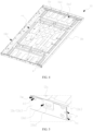
FIG. 1 is a schematic structural view illustrating a splicing display device according to one embodiment of the present application. -
FIG. 2 is a partial cross-sectional view illustrating the splicing display device according to one embodiment of the present application. -
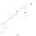
FIG. 3 is a schematic structural view illustrating a middle frame of the splicing display device according to one embodiment of the present application. -
FIG. 4 is a schematic structural view illustrating a backplate of the splicing display device according to one embodiment of the present application. -
FIG. 5 is an enlarged view of part A inFIG. 4 . -
FIG. 6 is an enlarged view of part B inFIG. 2 . -
FIG. 7 is a schematic structural view illustrating a support frame of the splicing display device according to one embodiment of the present application. -
FIG. 8 is an enlarged view of part C inFIG. 7 . - The technical solutions in the present application will be clearly and completely described below in conjunction with accompanying drawings and with reference to specific embodiments. Obviously, the embodiments are only some of the embodiments of the present application, rather than all the embodiments. Based on the embodiments in the present application, all other embodiments obtained by those skilled in the art without creative work shall fall within the protection scope of the present application. In addition, it should be understood that the specific embodiments described here are only used to illustrate and explain the present application, and are not used to limit the present application. In the present application, unless otherwise specified, directional terms such as "upper" and "lower" generally refer to the upper and lower directions of a device in actual use or work state, and specifically refer to the directions in the drawings. The terms "inner" and "outer" are referred to with reference to outlines of the device.
- The present application provides a splicing display device. Detailed descriptions are provided below. It should be noted that an order of descriptions in the following embodiments is not intended to limit a preferred order of the embodiments.
- It should be noted that, in the present application, the
display device 100 is a liquid crystal display device as an example for description, but the present application is not limited in this regard. For example, in the present application, the panel can also be a light emitting diode (LED) panel, such as a micro-LED panel, a mini-LED panel, an organic LED panel, or a quantum dot LED panel. - When the panel is an LED panel, the panel is placed in the receiving chamber rn of the
backplate 111. Thebackplate 111 and a connection structure between thebackplate 111 and a middle frame are described below, and a detailed description is omitted herein. - Please refer to
FIG. 1 and FIG. 2 . The present application provides asplicing display device 1000. The splicing display device comprises at least twodisplay devices 100, amiddle frame 200, and a light emitting diode (LED)substrate 300. - Each two
adjacent display devices 100 are spliced to form a gap fx. Eachdisplay device 100 comprises abackplate 111 and apanel 12 disposed on thebackplate 111. - With reference to
FIG. 3 , themiddle frame 200 comprises a carryingpart 21 and a fixingpart 22 connected to the carryingpart 21. The carryingpart 21 is arranged on twoadjacent panels 12 and shields the gap fx. The fixingpart 22 is arranged in the gap fx and is detachably connected to thebackplate 111. - The
LED substrate 300 is disposed on the carryingpart 21. - The
display device 100 comprises abacklight module 11 disposed on a light incident side of thepanel 12. Thebacklight module 11 comprises abackplate 111. - The
splicing display device 1000 of the present embodiment not only uses themiddle frame 200 to protect thepanels 12, but also uses themiddle frame 200 as a base for supporting theLED substrate 300. Themiddle frame 200 and thebacklight module 11 of thedisplay device 100 are detachably connected, and theLED substrate 300 is also arranged on the carryingpart 21 of themiddle frame 200. Therefore, by just detaching themiddle frame 200, theLED substrate 300 are separated from thepanels 12, which reduces the difficulty in detaching theLED substrate 300. - Optionally, the
LED substrate 300 can be an inorganic LED substrate or an organic light-emitting diode (OLED) substrate like a micro-LED substrate, a mini-LED substrate, or a quantum dot light-emitting diode (QLED) substrate. - Optionally, the
splicing display device 1000 further comprises aflexible circuit board 400. Theflexible circuit board 400 is connected to one side of theLED substrate 300 facing the gap fx. Anopening 21a is defined in the supportingpart 21. Theflexible circuit board 400 passes through theopening 21a and is disposed in the gap fx. - Through the
opening 21a defined in the carryingpart 21, theflexible circuit board 400 can pass through the carryingpart 21 and enter the gap fx. Such configuration avoids theflexible circuit board 400 from going around an outer surface of the carryingpart 21 to enter the gap fx, thereby reducing a height of theLED substrate 300, saving layout space, and shortening a length of theflexible circuit board 400. - In some embodiments, the carrying
part 21 can have no openings. In this case, theflexible circuit board 400 is bonded to a side or a front of theLED substrate 300, and theflexible circuit board 400 extends around the outer surface of the carryingpart 21 to enter the gap fx. - Optionally, a thickness d1 of the carrying
part 21 is less than a thickness d2 of the fixingpart 22. - The less thickness of the carrying
part 21 makes theLED substrate 300 disposed on thepanel 12 not visually obtrusive. The greater thickness of the fixingpart 22 improves stability in the connection between thesupport frame 112 and thebackplate 111. - Optionally, the
LED substrate 300 shields the carryingpart 21, and an edge portion of theLED substrate 300 protrudes beyond the carryingpart 21. - The
LED substrate 300 and the carryingpart 21 are both arranged in the non-display area NA. TheLED substrate 300 shields and protrudes beyond the carryingpart 21. Such configuration reduces a risk that the carryingpart 21 is saw in a side view angle and improves the display performance. - Optionally, the
panel 12 comprises a display area AA and a non-display area NA arranged on a periphery of the display area AA. The non-display area NA comprises a non-bonding area NA1 and a bonding area NA2 for bonding a circuit board. - With reference to
FIGs. 2 and3 , the carryingpart 21 comprises afirst portion 211 and asecond portion 212. Thefirst portion 211 is disposed on the bonding area NA2. Thesecond portion 212 is arranged on the non-bonding area NA1. A width of thefirst portion 211 is greater than a width of thesecond portion 212. - In splicing the two
display devices 100, the bonding area NA1 of the non-display area NA is at one side of the gap fx, and the non-bonding area NA1 is at another side of the gap fx. A width of the bonding area NA2 is greater than a width of the non-bonding area NA1. Therefore, by designing the width of thefirst portion 211 to be greater than the width of thesecond portion 212, the carryingpart 21 can better shield the non-display area NA, and better support theLED substrate 300. - Optionally, the
opening 21a is defined in thefirst part 211 and corresponding to the gap fx. Theflexible circuit board 400 is located at one side of the fixingpart 22 close to the bonding area NA2. - The bonding area NA2 is used to bond a flip chip or a non-flip chip circuit board, and the
flexible circuit board 400 is arranged on one side close to the bonding area NA2, so that both theflexible circuit board 400 and the circuit board bonded in the bonding area NA2 can connect to a driving board, which simplifies connection steps and saves installation space. - Optionally, referring to
FIG. 4 and FIG. 5 , thebacklight module 11 comprises thebackplate 111. Thebackplate 111 comprises abase 11a and a first surroundingwall 11b connected to a periphery of thebase 11a. Thebase 11a and the first surroundingwall 11b define a receiving chamber rn. A limiting recess Xw and a first hole k1 are defined in the first surroundingwall 11b. The first hole k1 is defined in a bottom of the limiting recess Xw. - With reference to
FIGs. 2 and3 , the fixingpart 22 comprises aplate body 221 and agroove body 222 protruding from theplate body 221. A second hole k2 is defined in thegroove body 222. Thegroove body 222 is disposed in the limiting recess Xw. Thegroove body 222 and thebackplate 111 are detachably connected by means of a connection element Lj. The connection member Lj is inserted through the first hole k1 and the second hole k2. - The
groove body 222 of the fixingpart 22 and the limiting recess Xw of thebackplate 111 cooperate to improve accuracy and convenience of assembling. In addition to that, a detachable connection between themiddle frame 200 and thebackplate 111 is realized by using the connection element Lj. - Please refer to
FIG. 6 . Optionally, the connection element Lj comprises a nut j 1 and a stud j2 connected to the nut j 1. The nut j 1 is arranged in a recessed groove br defined by thegroove body 222. The stud j2 is threadedly connected to the first hole k1. - By arranging the nut j 1 in the recessed groove br defined by the
groove body 222, the present application saves assembly space. By using the stud j2 threadedly connected to the first hole k1, the present application avoids unnecessary use of nuts, reduces the difficulty in connection, and saves materials. - In some embodiments, the connection element Lj can be a plug-in element, and the plug-in element is insertedly fitted into the first hole k1.
- Optionally, please continue to refer to
FIG. 4 , a plurality of platforms 11a1 protrudes from thebase 11a. The platforms 11a1 are used to place light boards. A plurality of heat dissipation grooves 11a2 are defined between the platforms 11a1 to facilitate heat dissipation of the light boards (a light source 113). - Optionally, please continue to refer to
FIG. 5 , an engagement groove 11b1 is defined in the first surroundingwall 11b, and an engagement block 11b2 is disposed in the engagement groove 11b1. By arranging the engagement block 11b2 in the engagement groove 11b1, the present application saves space for arranging the engagement block 11b2. The engagement block 11b2 is used for engagement with an engagement lug 11g of thesupport frame 112. The engagement lug 11g is arranged in the engagement groove 11b1. - The first
surrounding wall 11b comprises a side wall 11b3, and a plurality of side walls 11b3 are arranged on side edges of thebase 11a in a one-to-one correspondence. An interval jx and an expansion port kc are defined between two adjacent side walls 11b3. The interval jx and the expansion port kc communicate and separate the two adjacent side walls 11b3, so as to improve adaptability of the first surroundingwall 11b and prevent the first surroundingwall 11b from being squeezed. - In addition, the expansion port kc is located at one side of the gap jx close to the
base 11a, and the expansion port kc extends from the gap jx to the two adjacent side walls 11b3 to form a bottom space. When the two adjacent side walls 11b3 are squeezed outwards, the expansion port kc has a buffer effect, reducing a risk of a bottom of the side walls 11b3 being torn. - Optionally, the
display device 100 comprises thebacklight module 11 disposed on the light incident side of thepanel 12. Thebacklight module 11 comprises thebackplate 111 and thesupport frame 112. Thesupport frame 112 is arranged in the receiving chamber rn. Thesupport frame 112 is fixedly connected to thebackplate 111. - Referring to
FIGs. 2 ,7 , and8 , thesupport frame 112 comprises a second surroundingwall 11c, asupport plate 11d, a thirdsurrounding wall 11e, and a connectingwall 11f. The secondsurrounding wall 11c is arranged inside and along a periphery of the receiving chamber rn. Thesupport plate 11d is protrudingly disposed on an opposite side of the second surroundingwall 11c. The thirdsurrounding wall 11e surrounds around thesupport plate 11d and is disposed on the first surroundingwall 11b. The connectingwall 11f is arranged corresponding to the bonding area NA2 and extends from the thirdsurrounding wall 11e toward thebase 11a. The connectingwall 11f is located outside the first surrounding wall 1 1b. - The second
surrounding wall 11c is engaged with the first surroundingwall 11b. The connectingwall 11f is engaged with the first surroundingwall 11b. Such configuration realizes the connection between thesupport frame 112 and thebackplate 111, and improves the convenience and stability of the connection between thesupport frame 112 and thebackplate 111. - Optionally, in the
display device 1000, the second surroundingwall 11c comprises a first wall 11c1 and a second wall 11c2 disposed opposite to each other. The first wall 11c1 is located on one side away from the bonding area NA2. The first wall 11c1, the first surroundingwall 11b, and thesupport plate 11d define a first space s1. - The second wall 11c2, the first surrounding
wall 11b and thesupport plate 11d define a second space s2. - The first space s1 and the second space s2 facilitate heat dissipation of the
backlight module 11 on the one hand, and facilitates installing electrical components and the like in the first space s1 and/or the second space s2 on the other hand. Optionally, detachment lugs 11g are disposed on a third wall 11c3 and a fourth side wall 11c4. The detachment lug 11g is provided with an engagement slot 11g1. The engagement lug 11g is arranged in the engagement groove 11b1 of thebackplate 111, and the engagement block 11b2 is engaged inside the engagement slot 11g1. - Optionally, the second surrounding
wall 11c further comprises the third wall 11c3 and the fourth wall 11c4 that are arranged opposite to each other. The third wall 11c3 is connected at one side of the first wall 11c1 and the second wall 11c2. The fourth wall 11c4 is connected at another side of the first wall 11c1 and the second wall 11c2. The third wall 11c3 and the fourth wall 11c4 are engaged with the first surroundingwall 11b, so as to realize the detachable connection between thebackplate 111 and thesupport frame 112. - Optionally, the
backlight module 11 further comprises alight source 113, adiffuser plate 114, and anoptical film 115. Thelight source 113 is arranged in the receiving chamber rn. - The
support plate 11d and the thirdsurrounding wall 11e are connected to form a receiving groove fz. Thediffuser plate 114 is disposed in the receiving groove fz. Theoptical film 115 is disposed on the thirdsurrounding wall 11e and is located on a light emitting side of thediffuser plate 114. Such configuration reasonably arranges optical components and improves a utilization rate of space. - In some embodiments, the
backlight module 11 can also comprise thelight source 113, a light guide plate, and theoptical film 115. Thelight source 113 is arranged on one side of the receiving chamber rn. The light guide plate is arranged in the receiving chamber rn and located on the light emitting side of the light source. Theoptical film 115 is disposed on the light guide plate. - In other words, the
backlight module 11 can be an edge-lit backlight or a direct-lit backlight. The present application takes the direct-lit backlight as an example for description, but the present application is not limited in this regard. - The splicing display device of the present application comprises at least two display devices, a middle frame, and an LED substrate. Each two adjacent display devices are spliced to form a gap. Each display device comprises a backlight module and a panel arranged on the backlight module. The middle frame comprises a carrying part and a fixing part connected to the carrying part. The carrying part is arranged on two adjacent panels and covers the gap. The fixing part is arranged in the gap and is detachably connected to the backlight module. The LED substrate is disposed on the carrying part.
- That is to say, the present application not only uses the middle frame to protect the panel, but also uses the middle frame as a base for supporting the LED substrate. The middle frame and the backplate of the display device are detachably connected, the LED substrate is also arranged on the carrying part of the middle frame. Therefore, by just detaching the middle frame, the LED substrate can be separated from the panel at the same time, which reduces the difficulty in detaching the LED substrate.
- The above is a detailed description to the splicing display device of the present application. Specific examples are used in the present disclosure to illustrate working principles and embodiments of the present application. The descriptions of the above embodiments are only used for ease of understanding the present application. Those skilled in the art can modify the embodiments and the application range according to the ideas of the present application. In conclusion, the contents of the specification should not be construed as a limitation to the present application.
Claims (20)
- A splicing display device, comprising:at least two display devices, wherein two adjacent display devices are spliced to form a gap, and each of the display devices comprises a backplate and a panel disposed on the backplate;a middle frame, wherein the middle frame comprises a carrying part and a fixing part connected to the carrying part, the carrying part is arranged on two adjacent panels and covers the gap, and the fixing part is arranged in the gap and detachably connected to the backplate; anda light emitting diode (LED) substrate, wherein the LED substrate is arranged on the carrying part;wherein the splicing display device further comprises a flexible circuit board, the flexible circuit board is connected to one side of the LED substrate facing the gap, an opening is defined in the carrying part, and the flexible circuit board passes through the opening and is disposed in the gap;wherein the LED substrate covers the carrying part, and an edge portion of the LED substrate protrudes beyond the carrying part.
- The splicing display device according to claim 1, wherein the panel comprises a display area and a non-display area disposed on a periphery of the display area, and the non-display area comprises a non-bonding area and a bonding area for bonding a circuit board; and
the carrying part comprises a first portion and a second portion, the first portion is arranged in the bonding area, the second portion is arranged in the non-bonding area, and a width of the first portion is greater than a width of the second portion. - The splicing display device according to claim 2, wherein the opening is defined in the first part, and the flexible circuit board is located on one side of the fixing part close to the bonding area.
- The splicing display device according to claim 2, wherein the backplate comprises a base and a first surrounding wall connected on a periphery of the base, the base and the first surrounding wall define a receiving chamber, a limiting recess and a first hole are defined in the first surrounding wall, and the first hole is defined in a bottom of the limiting recess; and
the fixing part comprises a plate body and a groove body protruding from the plate body, a second hole is defined in the groove body, the groove body is disposed in the limiting recess, the groove body and the backplate are detachably connected by a connection element, and the connection element is inserted through the first hole and the second hole. - The splicing display device according to claim 4, wherein the connection element comprises a nut and a stud connected to the nut, the nut is arranged in a recessed groove defined by the groove body, and the stud is threadedly connected to the first hole.
- The splicing display device according to claim 4, wherein the panel is disposed in the receiving chamber of the backplate, and the panel is an LED panel.
- The splicing display device according to claim 1, wherein a thickness of the carrying part is less than a thickness of the fixing part.
- A splicing display device, comprising:at least two display devices, wherein two adjacent display devices are spliced to form a gap, and each of the display devices comprises a backplate and a panel disposed on the backplate;a middle frame, wherein the middle frame comprises a carrying part and a fixing part connected to the carrying part, the carrying part is arranged on two adjacent panels and covers the gap, and the fixing part is arranged in the gap and detachably connected to the backplate; anda light emitting diode (LED) substrate, wherein the LED substrate is arranged on the carrying part.
- The splicing display device according to claim 8, wherein the splicing display device further comprises a flexible circuit board, the flexible circuit board is connected to one side of the LED substrate facing the gap, an opening is defined in the carrying part, and the flexible circuit board passes through the opening and is disposed in the gap.
- The splicing display device according to claim 9, wherein the panel comprises a display area and a non-display area disposed on a periphery of the display area, and the non-display area comprises a non-bonding area and a bonding area for bonding a circuit board; and
the carrying part comprises a first portion and a second portion, the first portion is arranged in the bonding area, the second portion is arranged in the non-bonding area, and a width of the first portion is greater than a width of the second portion. - The splicing display device according to claim 10, wherein the opening is defined in the first part, and the flexible circuit board is located on one side of the fixing part close to the bonding area.
- The splicing display device according to claim 10, wherein the backplate comprises a base and a first surrounding wall connected on a periphery of the base, the base and the first surrounding wall define a receiving chamber, a limiting recess and a first hole are defined in the first surrounding wall, and the first hole is defined in a bottom of the limiting recess; and
the fixing part comprises a plate body and a groove body protruding from the plate body, a second hole is defined in the groove body, the groove body is disposed in the limiting recess, the groove body and the backplate are detachably connected by a connection element, and the connection element is inserted through the first hole and the second hole. - The splicing display device according to claim 12, wherein the connection element comprises a nut and a stud connected to the nut, the nut is arranged in a recessed groove defined by the groove body, and the stud is threadedly connected to the first hole.
- The splicing display device according to claim 12, wherein the panel is disposed in the receiving chamber of the backplate, and the panel is an LED panel.
- The splicing display device according to claim 12, wherein the display device comprises a backlight module arranged on a light incident side of the panel, the backlight module comprises the backplate and a support frame, the support frame is arranged in the receiving chamber, and the support frame is fixedly connected to the backplate;the support frame comprises a second surrounding wall, a support plate, a third surrounding wall, and a connecting wall, the second surrounding wall is arranged inside and along a periphery of the receiving chamber, the support plate is protrudingly disposed on an opposite side of the second surrounding wall, the third surrounding wall surrounds around the support plate and arranged on the first surrounding wall, the connecting wall is disposed corresponding to the bonding area and extends from the third surrounding wall to the base, and the connecting wall is located on an outer side with respect to the first surrounding wall; andthe second surrounding wall is engaged with the first surrounding wall, and the connecting wall is engaged with the first surrounding wall.
- The splicing display device according to claim 15, wherein the second surrounding wall comprises a first wall and a second wall that are arranged opposite to each other, and the first wall is located on one side away from the bonding area, and the first wall, the first surrounding wall, and the support plate define a first space; and
the second wall, the first surrounding wall, and the support plate define a second space. - The splicing display device according to claim 16, wherein the second surrounding wall further comprises a third wall and a fourth wall that are arranged opposite to each other, and the third wall is connected at one side of the first wall, the fourth wall is connected at another side of the first wall and the second wall, and the third wall and the fourth wall are engaged with the first surrounding wall.
- The splicing display device according to claim 16, wherein the backlight module further comprises a light source, a diffuser plate, and an optical film, and the light source is arranged in the receiving chamber; and
the support plate and the third surrounding wall are connected to form a receiving groove, the diffuser plate is disposed in the receiving groove, and the optical film is disposed on the third surrounding wall and located on a light emitting side of the diffuser plate. - The splicing display device according to claim 8, wherein a thickness of the carrying part is less than a thickness of the fixing part.
- The splicing display device according to claim 8, wherein the LED substrate shields the carrying part, and an edge portion of the LED substrate protrudes beyond the carrying part.
Applications Claiming Priority (2)
| Application Number | Priority Date | Filing Date | Title |
|---|---|---|---|
| CN202111345650.6A CN114005375A (en) | 2021-11-15 | 2021-11-15 | Mixed connection display device |
| PCT/CN2021/131760 WO2023082308A1 (en) | 2021-11-15 | 2021-11-19 | Hybrid tiled display device |
Publications (2)
| Publication Number | Publication Date |
|---|---|
| EP4435766A1 true EP4435766A1 (en) | 2024-09-25 |
| EP4435766A4 EP4435766A4 (en) | 2025-09-17 |
Family
ID=79928967
Family Applications (1)
| Application Number | Title | Priority Date | Filing Date |
|---|---|---|---|
| EP21827528.7A Pending EP4435766A4 (en) | 2021-11-15 | 2021-11-19 | HYBRID MOSAIC DISPLAY DEVICE |
Country Status (5)
| Country | Link |
|---|---|
| US (1) | US12255186B2 (en) |
| EP (1) | EP4435766A4 (en) |
| JP (1) | JP7520050B2 (en) |
| CN (2) | CN114005375A (en) |
| WO (1) | WO2023082308A1 (en) |
Families Citing this family (2)
| Publication number | Priority date | Publication date | Assignee | Title |
|---|---|---|---|---|
| CN114550609B (en) * | 2022-02-28 | 2023-01-17 | 长沙惠科光电有限公司 | Display panel and display device |
| TWI883785B (en) * | 2024-01-15 | 2025-05-11 | 友達光電股份有限公司 | Display device |
Family Cites Families (21)
| Publication number | Priority date | Publication date | Assignee | Title |
|---|---|---|---|---|
| JP2001159874A (en) * | 1999-12-01 | 2001-06-12 | Noboru Masuda | Illuminated display device |
| JP2007192977A (en) * | 2006-01-18 | 2007-08-02 | Seiko Epson Corp | Tiling display |
| TWM450917U (en) * | 2012-04-05 | 2013-04-11 | Harvatek Corp | TV wall |
| CN104464557B (en) * | 2013-09-24 | 2019-07-12 | 夏展敏 | A kind of edge shows the scheme integrated with liquid crystal display |
| KR102109660B1 (en) * | 2013-12-13 | 2020-05-12 | 엘지디스플레이 주식회사 | Liquid crystal display device |
| CN105845036A (en) * | 2015-01-14 | 2016-08-10 | 丁炜慷 | Whole seamless display curtain wall system with full coverage of pixel after splicing |
| CN106033156B (en) | 2015-03-12 | 2019-11-05 | 中强光电股份有限公司 | Display device and display method |
| KR102504236B1 (en) * | 2016-06-30 | 2023-02-27 | 엘지디스플레이 주식회사 | Display apparatus and multi screen display apparatus comprising the same |
| KR102740814B1 (en) * | 2016-12-20 | 2024-12-09 | 엘지디스플레이 주식회사 | Display apparatus and multi screen display apparatus comprising the same |
| CN106842711A (en) * | 2017-03-29 | 2017-06-13 | 韩玉君 | Display structure and integrated morphology for eliminating FPD platen edge piece |
| CN106972045B (en) * | 2017-04-14 | 2019-03-19 | 深圳市微阵技术有限公司 | Frameless display bar and screen splicing system |
| US20190058081A1 (en) * | 2017-08-18 | 2019-02-21 | Khaled Ahmed | Micro light-emitting diode (led) display and assembly apparatus |
| CN207199233U (en) * | 2017-09-28 | 2018-04-06 | 北京京东方显示技术有限公司 | A kind of display screen and mosaic screen |
| KR102707571B1 (en) * | 2019-01-04 | 2024-09-19 | 삼성전자주식회사 | Display appartus |
| CN110444124B (en) * | 2019-09-11 | 2024-12-31 | 宋清海 | A display device capable of reducing brightness difference between joint seam and display screen |
| CN111290154A (en) | 2020-02-24 | 2020-06-16 | 京东方科技集团股份有限公司 | Display device and spliced screen |
| CN211149981U (en) * | 2020-03-19 | 2020-07-31 | 深圳市晶创博科技有限公司 | Seamless splicing display screen |
| WO2021189433A1 (en) * | 2020-03-27 | 2021-09-30 | 京东方科技集团股份有限公司 | Strip-shaped display structure, display panel and display device |
| CN113763823B (en) * | 2021-11-10 | 2022-04-01 | Tcl华星光电技术有限公司 | Splicing display panel and splicing display device |
| CN114283698B (en) * | 2021-12-20 | 2023-05-30 | Tcl华星光电技术有限公司 | Spliced display panel and electronic equipment |
| CN114373396B (en) * | 2022-02-10 | 2023-10-17 | 惠州华星光电显示有限公司 | Spliced display panel and spliced display device |
-
2021
- 2021-11-15 CN CN202111345650.6A patent/CN114005375A/en active Pending
- 2021-11-19 WO PCT/CN2021/131760 patent/WO2023082308A1/en not_active Ceased
- 2021-11-19 CN CN202190001059.6U patent/CN222300249U/en active Active
- 2021-11-19 US US17/618,486 patent/US12255186B2/en active Active
- 2021-11-19 JP JP2021570214A patent/JP7520050B2/en active Active
- 2021-11-19 EP EP21827528.7A patent/EP4435766A4/en active Pending
Also Published As
| Publication number | Publication date |
|---|---|
| JP2024503149A (en) | 2024-01-25 |
| WO2023082308A1 (en) | 2023-05-19 |
| US12255186B2 (en) | 2025-03-18 |
| CN114005375A (en) | 2022-02-01 |
| JP7520050B2 (en) | 2024-07-22 |
| US20240014184A1 (en) | 2024-01-11 |
| EP4435766A4 (en) | 2025-09-17 |
| CN222300249U (en) | 2025-01-03 |
Similar Documents
| Publication | Publication Date | Title |
|---|---|---|
| KR101541352B1 (en) | Liquid crystal display device | |
| CN107272238B (en) | display device | |
| US10732920B2 (en) | Coupled display device | |
| JP5538495B2 (en) | Liquid crystal display module | |
| US9423640B2 (en) | Display device comprising a first positioning portion opposite to a second positioning portion and television device having the same | |
| KR102033481B1 (en) | Liquid crystal display device | |
| US9188800B2 (en) | Liquid crystal display device | |
| CN110168627A (en) | Display device | |
| KR20160064326A (en) | Tiled display device | |
| CN103765300A (en) | display device | |
| CN101666943A (en) | Liquid crystal display equipment | |
| US12255186B2 (en) | Splicing display device | |
| US20140192497A1 (en) | Display module and display device including the display module | |
| CN107621733A (en) | Side entrance back module | |
| KR20090046509A (en) | Liquid crystal display | |
| KR20130035120A (en) | Backlight unit and lcd moudule inclulding the same | |
| KR20140068734A (en) | Liquid crystal display apparatus | |
| US20160102847A1 (en) | Lighting device, display device, and television receiving device | |
| US20140132848A1 (en) | Illuminating device, display device, and television receiver | |
| US9581846B2 (en) | Display device and television device | |
| KR101795022B1 (en) | Led array and lcd module including the same | |
| KR20080067875A (en) | Back light assembly and display device having same | |
| CN102103278A (en) | Liquid crystal display device for preventing leakage of light at corner thereof | |
| KR101634632B1 (en) | Connecting structure of light emitting device substrate and flexible pinited circuit board, and liquid crystal display device having thereof | |
| KR20150115099A (en) | Display apparatus |
Legal Events
| Date | Code | Title | Description |
|---|---|---|---|
| STAA | Information on the status of an ep patent application or granted ep patent |
Free format text: STATUS: UNKNOWN |
|
| STAA | Information on the status of an ep patent application or granted ep patent |
Free format text: STATUS: THE INTERNATIONAL PUBLICATION HAS BEEN MADE |
|
| PUAI | Public reference made under article 153(3) epc to a published international application that has entered the european phase |
Free format text: ORIGINAL CODE: 0009012 |
|
| STAA | Information on the status of an ep patent application or granted ep patent |
Free format text: STATUS: REQUEST FOR EXAMINATION WAS MADE |
|
| 17P | Request for examination filed |
Effective date: 20211229 |
|
| AK | Designated contracting states |
Kind code of ref document: A1 Designated state(s): AL AT BE BG CH CY CZ DE DK EE ES FI FR GB GR HR HU IE IS IT LI LT LU LV MC MK MT NL NO PL PT RO RS SE SI SK SM TR |
|
| DAV | Request for validation of the european patent (deleted) | ||
| DAX | Request for extension of the european patent (deleted) | ||
| REG | Reference to a national code |
Ref country code: DE Ref legal event code: R079 Free format text: PREVIOUS MAIN CLASS: G09F0009302000 Ipc: G02F0001133300 |
|
| A4 | Supplementary search report drawn up and despatched |
Effective date: 20250821 |
|
| RIC1 | Information provided on ipc code assigned before grant |
Ipc: G02F 1/1333 20060101AFI20250814BHEP Ipc: G09F 9/302 20060101ALI20250814BHEP Ipc: H05K 1/18 20060101ALI20250814BHEP Ipc: H01L 25/075 20060101ALN20250814BHEP |