EP4435637A1 - Matrixberechnungsverfahren, chip und zugehörige vorrichtung - Google Patents
Matrixberechnungsverfahren, chip und zugehörige vorrichtung Download PDFInfo
- Publication number
- EP4435637A1 EP4435637A1 EP22909746.4A EP22909746A EP4435637A1 EP 4435637 A1 EP4435637 A1 EP 4435637A1 EP 22909746 A EP22909746 A EP 22909746A EP 4435637 A1 EP4435637 A1 EP 4435637A1
- Authority
- EP
- European Patent Office
- Prior art keywords
- multiplexer
- vector
- buffer
- group
- path
- Prior art date
- Legal status (The legal status is an assumption and is not a legal conclusion. Google has not performed a legal analysis and makes no representation as to the accuracy of the status listed.)
- Pending
Links
Images


Classifications
-
- G—PHYSICS
- G06—COMPUTING OR CALCULATING; COUNTING
- G06F—ELECTRIC DIGITAL DATA PROCESSING
- G06F3/00—Input arrangements for transferring data to be processed into a form capable of being handled by the computer; Output arrangements for transferring data from processing unit to output unit, e.g. interface arrangements
- G06F3/06—Digital input from, or digital output to, record carriers, e.g. RAID, emulated record carriers or networked record carriers
-
- G—PHYSICS
- G06—COMPUTING OR CALCULATING; COUNTING
- G06F—ELECTRIC DIGITAL DATA PROCESSING
- G06F5/00—Methods or arrangements for data conversion without changing the order or content of the data handled
- G06F5/06—Methods or arrangements for data conversion without changing the order or content of the data handled for changing the speed of data flow, i.e. speed regularising or timing, e.g. delay lines, FIFO buffers; over- or underrun control therefor
- G06F5/16—Multiplexed systems, i.e. using two or more similar devices which are alternately accessed for enqueue and dequeue operations, e.g. ping-pong buffers
-
- G—PHYSICS
- G06—COMPUTING OR CALCULATING; COUNTING
- G06F—ELECTRIC DIGITAL DATA PROCESSING
- G06F17/00—Digital computing or data processing equipment or methods, specially adapted for specific functions
- G06F17/10—Complex mathematical operations
- G06F17/16—Matrix or vector computation, e.g. matrix-matrix or matrix-vector multiplication, matrix factorization
-
- G—PHYSICS
- G06—COMPUTING OR CALCULATING; COUNTING
- G06F—ELECTRIC DIGITAL DATA PROCESSING
- G06F3/00—Input arrangements for transferring data to be processed into a form capable of being handled by the computer; Output arrangements for transferring data from processing unit to output unit, e.g. interface arrangements
- G06F3/06—Digital input from, or digital output to, record carriers, e.g. RAID, emulated record carriers or networked record carriers
- G06F3/0601—Interfaces specially adapted for storage systems
- G06F3/0628—Interfaces specially adapted for storage systems making use of a particular technique
- G06F3/0655—Vertical data movement, i.e. input-output transfer; data movement between one or more hosts and one or more storage devices
- G06F3/0656—Data buffering arrangements
-
- G—PHYSICS
- G06—COMPUTING OR CALCULATING; COUNTING
- G06F—ELECTRIC DIGITAL DATA PROCESSING
- G06F7/00—Methods or arrangements for processing data by operating upon the order or content of the data handled
- G06F7/38—Methods or arrangements for performing computations using exclusively denominational number representation, e.g. using binary, ternary, decimal representation
- G06F7/48—Methods or arrangements for performing computations using exclusively denominational number representation, e.g. using binary, ternary, decimal representation using non-contact-making devices, e.g. tube, solid state device; using unspecified devices
- G06F7/52—Multiplying; Dividing
- G06F7/523—Multiplying only
-
- G—PHYSICS
- G06—COMPUTING OR CALCULATING; COUNTING
- G06F—ELECTRIC DIGITAL DATA PROCESSING
- G06F8/00—Arrangements for software engineering
- G06F8/30—Creation or generation of source code
- G06F8/36—Software reuse
-
- G—PHYSICS
- G06—COMPUTING OR CALCULATING; COUNTING
- G06F—ELECTRIC DIGITAL DATA PROCESSING
- G06F9/00—Arrangements for program control, e.g. control units
- G06F9/06—Arrangements for program control, e.g. control units using stored programs, i.e. using an internal store of processing equipment to receive or retain programs
- G06F9/30—Arrangements for executing machine instructions, e.g. instruction decode
- G06F9/38—Concurrent instruction execution, e.g. pipeline or look ahead
- G06F9/3836—Instruction issuing, e.g. dynamic instruction scheduling or out of order instruction execution
-
- G—PHYSICS
- G06—COMPUTING OR CALCULATING; COUNTING
- G06F—ELECTRIC DIGITAL DATA PROCESSING
- G06F7/00—Methods or arrangements for processing data by operating upon the order or content of the data handled
- G06F7/38—Methods or arrangements for performing computations using exclusively denominational number representation, e.g. using binary, ternary, decimal representation
- G06F7/48—Methods or arrangements for performing computations using exclusively denominational number representation, e.g. using binary, ternary, decimal representation using non-contact-making devices, e.g. tube, solid state device; using unspecified devices
- G06F7/544—Methods or arrangements for performing computations using exclusively denominational number representation, e.g. using binary, ternary, decimal representation using non-contact-making devices, e.g. tube, solid state device; using unspecified devices for evaluating functions by calculation
- G06F7/5443—Sum of products
-
- Y—GENERAL TAGGING OF NEW TECHNOLOGICAL DEVELOPMENTS; GENERAL TAGGING OF CROSS-SECTIONAL TECHNOLOGIES SPANNING OVER SEVERAL SECTIONS OF THE IPC; TECHNICAL SUBJECTS COVERED BY FORMER USPC CROSS-REFERENCE ART COLLECTIONS [XRACs] AND DIGESTS
- Y02—TECHNOLOGIES OR APPLICATIONS FOR MITIGATION OR ADAPTATION AGAINST CLIMATE CHANGE
- Y02D—CLIMATE CHANGE MITIGATION TECHNOLOGIES IN INFORMATION AND COMMUNICATION TECHNOLOGIES [ICT], I.E. INFORMATION AND COMMUNICATION TECHNOLOGIES AIMING AT THE REDUCTION OF THEIR OWN ENERGY USE
- Y02D10/00—Energy efficient computing, e.g. low power processors, power management or thermal management
Definitions
- This application relates to the computer field, and in particular, to a matrix computing method, a chip, and a related device.
- a large quantity of matrix multiplication operations are involved, for example, in a scenario such as AI model training or AI inference.
- AI Artificial Intelligence
- HPC high-performance computing
- a matrix is usually sparsified by using a pruning technology, and then computing is performed by using a sparsified matrix, to reduce a computing amount in a computing process.
- structured pruning is performed on a weight matrix obtained through training to complete sparsification of the weight matrix.
- a weight matrix obtained through structured pruning is used for inference.
- the foregoing method supports only computing by using a pruned matrix after pruning a determined matrix, and does not support a scenario in which a sparsity degree of a matrix dynamically changes in the computing process.
- This application provides a matrix computing method, a chip, and a related device, to support computing of a matrix whose sparsity degree dynamically changes, reduce a computing amount in the computing, and improve computing efficiency without reducing computing precision.
- this application provides a chip.
- the chip includes a first buffer, a second buffer, a first scheduling module, and a first processing element.
- the first buffer is configured to buffer a first vector
- the second buffer is configured to buffer a second vector.
- the first scheduling module is configured to generate a first selection signal based on a bitmap of the first vector.
- the first selection signal may cause the first processing element to obtain, from the first buffer, a first group of non-zero elements in the first vector, and cause the first processing element to obtain, from the second buffer, a second group of elements in the second vector.
- the first processing element is configured to implement an operation between the first vector and the second vector based on the first group of non-zero elements in the first vector and the second group of elements in the second vector.
- the bitmap of the first vector indicates a non-zero element in the first vector.
- Each bit in the bitmap of the first vector corresponds to one element in the first vector, and a value of each bit indicates whether the corresponding element in the first vector is 0. For example, if a value of a bit is 0, it indicates that a value of a corresponding element in the first vector is 0. If a value of a bit is 1, it indicates that a value of a corresponding element in the first vector is not 0.
- the first scheduling module may determine, based on the bitmap of the first vector, elements that are non-zero elements in the first vector, so that the first processing element may obtain only the non-zero element in the first vector, then obtain an element at a corresponding position from the second vector, and perform the operation between the first vector and the second vector, to reduce a computing amount and improve computing efficiency.
- a value obtained by multiplying an element whose element value is 0 in one vector by a non-zero element in another vector is 0, and a result of performing a dot product of two vectors is not affected. Therefore, only the non-zero element in the first vector is obtained to perform the operation between the first vector and the second vector, and computing precision is not reduced.
- the chip further includes a first multiplexer and a second multiplexer.
- the first multiplexer is configured to obtain, from the first buffer, the first group of non-zero elements in the first vector based on the first selection signal, and input the first group of non-zero elements into the first processing element.
- the second multiplexer is configured to obtain, from the second buffer, the second group of elements in the second vector based on the first selection signal, and input the second group of elements into the first processing element.
- the first multiplexer and the second multiplexer each include K multi-path multiplexers.
- the first buffer and the second buffer each include W rows and K columns of data units, and each data unit is configured to buffer one element in a vector or matrix.
- Each multi-path multiplexer in the first multiplexer is connected to a plurality of data units in the first buffer, and each data unit is connected to at least one multi-path multiplexer.
- a connection relationship between an i th multi-path multiplexer in the second multiplexer and a data unit in the second buffer is the same as a connection relationship between an i th multi-path multiplexer in the first multiplexer and a data unit in the first buffer.
- a multiplication operation needs to be performed between an r th element in the first vector and an r th element in the second vector.
- a relative position in which the r th element in the first vector is stored in the first buffer is the same as a relative position in which the r th element in the second vector is stored in the second buffer.
- the r th element in the first vector is stored in an r th data unit in a 1 st row in the first buffer
- the r th element in the second vector is stored in an r th data unit in a 1 st row in the second buffer.
- the i th multi-path multiplexer in the first multiplexer is connected to the plurality of data units in the first buffer.
- Relative positions of the plurality of data units in the first buffer are the same as relative positions, in the second buffer, of a plurality of data units in the second buffer that are connected to the i th multi-path multiplexer in the second multiplexer.
- the i th multi-path multiplexer in the first multiplexer is connected to a 2 nd data unit in the 1 st row and a 5 th data unit in a 2 nd row in the first buffer
- the i th multi-path multiplexer in the second multiplexer is connected to a 2 nd data unit in the 1 st row and a 5 th data unit in a 2 nd row in the second buffer.
- the i th multi-path multiplexer in the first multiplexer and the i th multi-path multiplexer in the second multiplexer can read, based on a same selection signal, data in data units whose relative positions are the same in the first buffer and the second buffer, and the first multiplexer and the second multiplexer read, based on the same selection signal, exactly elements that need to be multiplied in the first vector and the second vector.
- the first scheduling module is specifically configured to: determine, based on the bitmap of the first vector, that an element stored in a k th data unit in data units connected to a j th multi-path multiplexer in the first multiplexer is a non-zero element.
- the first scheduling module generates a selection signal of the j th multi-path multiplexer in the first multiplexer, and sends the selection signal of the j th multi-path multiplexer in the first multiplexer to the j th multi-path multiplexer in the first multiplexer and a j th multi-path multiplexer in the second multiplexer.
- the first selection signal includes the selection signal of the j th multi-path multiplexer in the first multiplexer.
- the first multiplexer includes K multi-path multiplexers, and the first scheduling module generates, selection signals respectively corresponding to the K multi-path multiplexers in one periodicity.
- the first selection signal includes the selection signals respectively corresponding to the K multi-path multiplexers, so that multi-path multiplexers in the first multiplexer and the second multiplexer separately read, based on a received selection signal, one piece of data from a connected data unit.
- a plurality of data units connected to one multi-path multiplexer above have different priorities.
- the first scheduling module Before generating a selection signal of one multi-path multiplexer, the first scheduling module first determines, based on the bitmap of the first vector, whether an element in the first vector stored in a data unit with a highest priority in data units connected to the multi-path multiplexer is 0. If the element stored in the data unit with the highest priority is not 0, a selection signal corresponding to the data unit with a 1 st priority is generated; or if the element stored in the data unit with the highest priority is 0, whether an element stored in a data unit with a 2 nd priority is 0 is further determined based on the bitmap of the first vector.
- a selection signal corresponding to the data unit with the 2 nd priority is generated; or if the element stored in the data unit with the 2 nd priority is 0, whether an element stored in a data unit with a 3 rd priority is 0 is further determined based on the bitmap of the first vector. The rest may be deduced by analogy, until a selection signal of the multi-path multiplexer is generated. By setting priorities, elements in a plurality of data units connected to multi-path multiplexers may be read in sequence.
- the first scheduling module needs to set a bit position in the bitmap corresponding to the element stored in the data unit to 0, to prevent the element in the data unit from being read again to cause a computing error.
- the first multiplexer is specifically configured to: obtain, based on the selection signal of the j th multi-path multiplexer in the first multiplexer and by using the j th multi-path multiplexer in the first multiplexer, a first element in the k th data unit in the data units connected to the j th multi-path multiplexer in the first multiplexer, and input the first element into the first processing element, where the first element is one of the first group of non-zero elements.
- the second multiplexer is specifically configured to obtain, based on the selection signal of the j th multi-path multiplexer in the first multiplexer and by using the j th multi-path multiplexer in the second multiplexer, a second element in a k th data unit in data units connected to the j th multi-path multiplexer in the second multiplexer, and input the second element into the first processing element, where the second element is one of the second group of elements.
- the first scheduling module sequentially generates the selection signals respectively corresponding to the K multi-path multiplexers in the first multiplexer, so that the first multiplexer and the second multiplexer separately extract K elements from connected buffers, and implement a dot product of the first vector and the second vector based on the extracted K pairs of data.
- the first multiplexer may not extract all non-zero elements from the first buffer in one periodicity.
- the first multiplexer may extract K non-zero elements at a time, and the first buffer stores W rows and K columns of elements. Therefore, after a maximum of W periodicities, all the non-zero elements in the first buffer may be extracted, to complete the operation between the first vector and the second vector.
- the first scheduling module after the first processing element completes the operation between the first vector and the second vector, the first scheduling module generates an erasing signal.
- the erasing signal indicates the first buffer and the second buffer to erase currently buffered data, to buffer data required for next computing.
- the first vector may be a part of a vector, and the second vector may be a part of another vector; or the first vector is a row vector, and the second vector is a column in a matrix; or the first vector belongs to any row in a first matrix, and the second vector belongs to any column in a second matrix.
- the chip can implement an operation between vectors, an operation between a vector and a matrix, or an operation between matrices through a plurality of times of the foregoing computing process.
- the chip further includes a third buffer and a second processing element.
- the third buffer is configured to buffer a third vector, where the third vector belongs to a column in the second matrix other than a column in which the second vector is located, and the first selection signal is further used to cause the second processing element to obtain, from the third buffer, a third group of elements in the third vector.
- the second processing element is configured to implement an operation between the first vector and the third vector based on the first group of non-zero elements and the third group of elements.
- the third buffer and the second processing element are added, the operation between the first vector and the third vector can be completed by using the second processing element, and the operation between the first vector and the second vector can be completed by using the first processing element.
- the second vector and the third vector both belong to the second matrix, so that the chip can implement the operation between a vector and a matrix.
- the chip further includes a third multiplexer, and the third multiplexer is configured to obtain, from the third buffer, the third group of elements in the third vector based on the first selection signal, and input the third group of elements into the second processing element.
- the third multiplexer includes K multi-path multiplexers
- the third buffer includes W rows and K columns of data units
- each data unit is configured to buffer one element.
- a connection relationship between an i th multi-path multiplexer in the third multiplexer and a data unit in the third buffer is the same as the connection relationship between the i th multi-path multiplexer in the first multiplexer and the data unit in the first buffer.
- the third multiplexer is configured to obtain, from the third buffer, an element in the third vector, and input the element into the second processing element, so that the second processing element implements the operation between the first vector and the third vector.
- a multiplication operation needs to be performed between the r th element in the first vector and an r th element in the third vector.
- the r th element in the first vector is stored in the r th data unit in the 1 st row in the first buffer
- the r th element in the third vector is stored in an r th data unit in a 1 st row in the third buffer.
- the i th multi-path multiplexer in the first multiplexer is connected to the plurality of data units in the first buffer. Relative positions of the plurality of data units in the first buffer are the same as relative positions, in the third buffer, of a plurality of data units in the third buffer that are connected to the i th multi-path multiplexer in the third multiplexer.
- the i th multi-path multiplexer in the first multiplexer is connected to the 2 nd data unit in the 1 st row and the 5 th data unit in the 2 nd row in the first buffer
- the i th multi-path multiplexer in the third multiplexer is connected to a 2 nd data unit in the 1 st row and a 5 th data unit in a 2 nd row in the third buffer.
- the i th multi-path multiplexer in the first multiplexer and the i th multi-path multiplexer in the third multiplexer can read, based on a same selection signal, data in data units whose relative positions are the same in the first buffer and the third buffer, and the first multiplexer and the third multiplexer read, based on the same selection signal, exactly elements that need to be multiplied in the first vector and the third vector.
- the third multiplexer is specifically configured to: obtain, based on the selection signal of the j th multi-path multiplexer in the first multiplexer and by using a j th multi-path multiplexer in the third multiplexer, a third element in a k th data unit in data units connected to the j th multi-path multiplexer in the third multiplexer, and input the third element into the second processing element, where the third element is one of the third group of elements.
- the chip further includes a fourth buffer, a second scheduling module, and a third processing element.
- the fourth buffer is configured to buffer a fourth vector, and the fourth vector belongs to a row in the first matrix other than a row in which the first vector is located.
- the second scheduling module is configured to generate a second selection signal based on a bitmap of a fourth vector.
- the second selection signal is used to cause the third processing element to obtain, from the fourth buffer, a fourth group of non-zero elements in the fourth vector, cause the third processing element to obtain, from the second buffer, a fifth group of elements in the second vector, and the bitmap of the fourth vector indicates a non-zero element in the fourth vector.
- the third processing element is configured to implement an operation between the fourth vector and the second vector based on the fourth group of non-zero elements and the fifth group of elements.
- the fourth buffer, the second scheduling module, and the third processing element are further added.
- the operation between the fourth vector in the first matrix and the second vector in the second matrix can be completed by using the third processing element, the operation between the first vector in the first matrix and the third vector in the second matrix can be completed by using the second processing element, and the operation between the first vector in the first matrix and the second vector in the second matrix can be completed by using the first processing element, so that the chip can implement the operation between matrices.
- the chip further includes a fourth multiplexer and a fifth multiplexer.
- the fourth multiplexer is configured to obtain, from the fourth buffer, the fourth group of non-zero elements in the fourth vector based on the second selection signal, and input the fourth group of non-zero elements into the third processing element.
- the fifth multiplexer is configured to obtain, from the second buffer, the fifth group of elements in the second vector based on the second selection signal, and input the fifth group of elements into the third processing element.
- the fourth multiplexer includes K multi-path multiplexers, and the fifth multiplexer includes K multi-path multiplexers.
- the fourth buffer includes W rows and K columns of data units, and each data unit is configured to buffer one element.
- Each multi-path multiplexer in the fourth multiplexer is connected to a plurality of data units in the fourth buffer, and each data unit is connected to at least one multi-path multiplexer.
- a connection relationship between an i th multi-path multiplexer in the fourth multiplexer and a data unit in the fourth buffer is the same as the connection relationship between the i th multi-path multiplexer in the first multiplexer and the data unit in the first buffer.
- a connection relationship between an i th multi-path multiplexer in the fifth multiplexer and the data unit in the second buffer is the same as the connection relationship between the i th multi-path multiplexer in the first multiplexer and the data unit in the first buffer.
- the fifth multiplexer may alternatively be connected to a fifth buffer.
- the fifth multiplexer is configured to obtain an element in the second vector, and the second vector is buffered in the second buffer, the fifth multiplexer may share the second buffer with the second multiplexer, to reduce complexity of the chip, reduce a size of the chip, and reduce costs.
- the fourth multiplexer is configured to obtain, from the fourth buffer, an element in the third vector, and input the element into the third processing element, so that the third processing element implements the operation between the fourth vector and the second vector.
- a multiplication operation needs to be performed between an r th element in the fourth vector and the r th element in the second vector.
- the r th element in the second vector is stored in the r th data unit in the 1 st row in the second buffer
- the r th element in the fourth vector is stored in an r th data unit in a 1 st row in the fourth buffer.
- the i th multi-path multiplexer in the fourth multiplexer is connected to the plurality of data units in the fourth buffer. Relative positions of the plurality of data units in the fourth buffer are the same as relative positions, in the second buffer, of the plurality of data units in the second buffer that are connected to the i th multi-path multiplexer in the fifth multiplexer.
- the i th multi-path multiplexer in the fourth multiplexer and the i th multi-path multiplexer in the fifth multiplexer can read, based on a same selection signal, data in data units whose relative positions are the same in the fourth buffer and the second buffer, and the fourth multiplexer and the fifth multiplexer read, based on the same selection signal, exactly elements that need to be multiplied in the fourth vector and the second vector.
- the second scheduling module is specifically configured to determine, based on the bitmap of the fourth vector, that an element stored in an m th data unit in data units connected to a j th multi-path multiplexer in the fourth multiplexer is a non-zero element.
- the second scheduling module generates a selection signal of the j th multi-path multiplexer, and sends the selection signal of the j th multi-path multiplexer to the j th multi-path multiplexer in the fourth multiplexer and a j th multi-path multiplexer in the fifth multiplexer.
- the second selection signal includes the selection signal of the j th multi-path multiplexer in the fourth multiplexer.
- the fourth multiplexer is specifically configured to: obtain, based on the selection signal of the j th multi-path multiplexer in the fourth multiplexer and by using the j th multi-path multiplexer in the fourth multiplexer, a fourth element in the m th data unit in the data units connected to the j th multi-path multiplexer of the fourth multiplexer, and input the fourth element into the third processing element, where the fourth element is one of the fourth group of non-zero elements.
- the fifth multiplexer is specifically configured to: obtain, based on the selection signal of the j th multi-path multiplexer in the fourth multiplexer and by using the j th multi-path multiplexer in the fifth multiplexer, a fifth element in an m th data unit in data units connected to the j th multi-path multiplexer in the fifth multiplexer, and input the fifth element into the third processing element, where the fifth element is one of the fifth group of elements.
- the second scheduling module sequentially generates selection signals respectively corresponding to the K multi-path multiplexers in the fourth multiplexer, so that the fourth multiplexer and the fifth multiplexer separately extract K elements from connected buffers, and implement a dot product of the fourth vector and the second vector based on the extracted K pairs of data.
- the fourth multiplexer may not extract all non-zero elements from the fourth buffer in one periodicity.
- the fourth multiplexer may extract K non-zero elements at a time, and the fourth buffer stores W rows and K columns of elements. Therefore, after a maximum of W periodicities, all the non-zero elements in the fourth buffer may be extracted, to complete the operation between the fourth vector and the second vector.
- this application provides a matrix computing method, applied to a chip.
- the chip includes a first buffer, a second buffer, a first scheduling module, and a first processing element, and the method includes: The chip buffers a first vector by using the first buffer, and buffers a second vector by using the second buffer.
- the first scheduling module of the chip After the chip buffers the first vector and the second vector, the first scheduling module of the chip generates a first selection signal based on a bitmap of the first vector, where the first selection signal may cause the first processing element to obtain, from the first buffer, a first group of non-zero elements in the first vector, cause the first processing element to obtain, from the second buffer, a second group of elements in the second vector, and the bitmap of the first vector indicates a non-zero element in the first vector. Then, the chip implements an operation between the first vector and the second vector by using the first processing element and based on the first group of non-zero elements and the second group of elements.
- the chip further includes a first multiplexer and a second multiplexer.
- the first multiplexer of the chip obtains, from the first buffer, the first group of non-zero elements in the first vector based on the first selection signal, and inputs the first group of non-zero elements into the first processing element.
- the second multiplexer of the chip obtains, from the second buffer, the second group of elements in the second vector based on the first selection signal, and inputs the second group of elements into the first processing element.
- the first multiplexer and the second multiplexer each include K multi-path multiplexers.
- the first buffer and the second buffer both include W rows and K columns of data units, and each data unit is configured to buffer one element.
- Each multi-path multiplexer in the first multiplexer is connected to a plurality of data units in the first buffer, and each data unit is connected to at least one multi-path multiplexer.
- a connection relationship between an i th multi-path multiplexer in the second multiplexer and a data unit in the second buffer is the same as a connection relationship between an i th multi-path multiplexer in the first multiplexer and a data unit in the first buffer.
- that the first scheduling module of the chip generates a first selection signal based on a bitmap of the first vector includes: The chip determines, based on the bitmap of the first vector, that an element stored in a k th data unit in data units connected to a j th multi-path multiplexer in the first multiplexer is a non-zero element.
- the first scheduling module generates a selection signal of the j th multi-path multiplexer, and sends the selection signal of the j th multi-path multiplexer to the j th multi-path multiplexer in the first multiplexer and a j th multi-path multiplexer in the second multiplexer.
- the first selection signal includes the selection signal of the j th multi-path multiplexer in the first multiplexer.
- the second multiplexer of the chip obtains, based on the selection signal of the j th multi-path multiplexer in the first multiplexer and by using the j th multi-path multiplexer in the second multiplexer, a second element in a k th data unit in data units connected to the j th multi-path multiplexer in the second multiplexer, and inputs the second element into the first processing element.
- the first element is one of the first group of non-zero elements
- the second element is one of the second group of elements.
- the first vector belongs to any row in a first matrix
- the second vector belongs to any column in a second matrix.
- the first vector may be a part or all of elements in any row in a matrix
- the second vector may be a part or all of elements in any column in another matrix.
- the chip further includes a third buffer and a second processing element.
- the method further includes: The chip buffers a third vector by using the third buffer, where the third vector belongs to a column in the second matrix other than a column in which the second vector is located.
- the first selection signal further causes the second processing element to obtain, from the third buffer, a third group of elements in the third vector.
- the second processing element of the chip implements an operation between the first vector and the third vector based on the first group of non-zero elements and the third group of elements.
- the chip further includes a third multiplexer.
- the method further includes: The third multiplexer of the chip obtains, from the third buffer, the third group of elements in the third vector based on the first selection signal, and inputs the third group of elements into the second processing element.
- the third multiplexer includes K multi-path multiplexers
- the third buffer includes W rows and K columns of data units
- each data unit is configured to buffer one element.
- a connection relationship between an i th multi-path multiplexer in the third multiplexer and a data unit in the third buffer is the same as the connection relationship between the i th multi-path multiplexer in the first multiplexer and the data unit in the first buffer.
- that the third multiplexer of the chip obtains, from the third buffer, the third group of elements in the third vector based on the first selection signal, and inputs the third group of elements into the second processing element includes the following.
- the chip further includes a fourth buffer, a second scheduling module, and a third processing element.
- the method further includes: The chip buffers a fourth vector by using the fourth buffer, where the fourth vector belongs to a row in the first matrix other than a row in which the first vector is located.
- the second scheduling module of the chip generates a second selection signal based on a bitmap of the fourth vector, where the second selection signal is used to cause the third processing element to obtain, from the fourth buffer, a fourth group of non-zero elements in the fourth vector, cause the third processing element to obtain, from the second buffer, a fifth group of elements in the second vector, and the bitmap of the fourth vector indicates a non-zero element in the fourth vector.
- the third processing element of the chip implements an operation between the fourth vector and the second vector based on the fourth group of non-zero elements and the fifth group of elements.
- the chip further includes a fourth multiplexer and a fifth multiplexer.
- the method further includes: The fourth multiplexer of the chip obtains, from the fourth buffer, the fourth group of non-zero elements in the fourth vector based on the second selection signal, and inputs the fourth group of non-zero elements into the third processing element.
- the fifth multiplexer of the chip obtains, from the second buffer, the fifth group of elements in the second vector based on the second selection signal, and inputs the fifth group of elements into the third processing element.
- the fourth multiplexer and the fifth multiplexer each include K multi-path multiplexers.
- the fourth buffer includes W rows and K columns of data units, and each data unit is configured to buffer one element.
- Each multi-path multiplexer in the fourth multiplexer is connected to a plurality of data units in the fourth buffer, and each data unit is connected to at least one multi-path multiplexer.
- a connection relationship between an i th multi-path multiplexer in the fourth multiplexer and a data unit in the fourth buffer is the same as the connection relationship between the i th multi-path multiplexer in the first multiplexer and the data unit in the first buffer.
- a connection relationship between an i th multi-path multiplexer in the fifth multiplexer and the data unit in a fifth buffer is the same as the connection relationship between the i th multi-path multiplexer in the first multiplexer and the data unit in the first buffer.
- that the second scheduling module of the chip generates a second selection signal based on a bitmap of the fourth vector includes: determining, based on the bitmap of the fourth vector, that an element stored in an m th data unit in data units connected to a j th multi-path multiplexer in the fourth multiplexer is a non-zero element.
- the second scheduling module generates a selection signal of the j th multi-path multiplexer, and sends the selection signal of the j th multi-path multiplexer to the j th multi-path multiplexer in the fourth multiplexer and a j th multi-path multiplexer in the fifth multiplexer.
- the second selection signal includes the selection signal of the j th multi-path multiplexer in the fourth multiplexer.
- the fifth multiplexer of the chip obtains, based on the selection signal of the j th multi-path multiplexer in the fourth multiplexer and by using the j th multi-path multiplexer in the fifth multiplexer, a fifth element in an m th data unit in data units connected to the j th multi-path multiplexer in the fifth multiplexer, and inputs the fifth element into the third processing element.
- the fourth element is one of the fourth group of non-zero elements
- the fifth element is one of the fifth group of elements.
- this application provides a matrix computing apparatus, including a first scheduling unit and a first processing unit.
- the first scheduling unit is configured to generate a first selection signal based on a bitmap of a first vector.
- the first selection signal may cause the first processing unit to obtain, from a first buffer, a first group of non-zero elements in the first vector, and cause the first processing unit to obtain, from a second buffer, a second group of elements in a second vector.
- the first processing unit is configured to implement an operation between the first vector and the second vector based on the first group of non-zero elements in the first vector and the second group of elements in the second vector, and the bitmap of the first vector indicates a non-zero element in the first vector.
- the first scheduling unit After the first processing unit implements the operation between the first vector and the second vector based on the first group of non-zero elements and the second group of elements, the first scheduling unit generates an erasing signal, where the erasing signal indicates the first buffer and the second buffer to erase data currently buffered by the first buffer and the second buffer.
- the first vector belongs to a part or all of elements in any row in a first matrix
- the second vector belongs to a part or all of elements in any column in a second matrix
- the matrix computing apparatus further includes a second processing unit, and the first selection signal may further cause the second processing unit to obtain a third group of elements in a third vector.
- the second processing unit is configured to implement an operation between the first vector and the third vector based on the first group of non-zero elements and the third group of elements.
- the third vector belongs to a column in the second matrix other than a column in which the second vector is located.
- the matrix computing apparatus further includes a second scheduling unit and a third processing unit.
- the second scheduling unit is configured to generate a second selection signal based on a bitmap of a fourth vector, where the second selection signal is used to cause a third processing unit to obtain a fourth group of non-zero elements in the fourth vector, and cause the third processing unit to obtain a fifth group of elements in the second vector.
- the bitmap of the fourth vector indicates a non-zero element in the fourth vector, and the fourth vector belongs to a row in the first matrix other than a row in which the first vector is located.
- the third processing unit is configured to implement an operation between the fourth vector and the second vector based on the fourth group of non-zero elements and the fifth group of elements.
- this application provides a computing device, where the computing device includes a chip and a memory.
- the memory is configured to store code, and the chip executes the code to implement the method in any one of the second aspect or the possible implementations of the second aspect.
- this application provides a computer-readable storage medium, the computing device-readable storage medium stores instructions.
- the computing device When the instructions are run on a computing device, the computing device performs the method in any one of the second aspect or the possible implementations of the second aspect.
- a computer program product including instructions is provided, including a computer program or instructions.
- the computing device is caused to perform the method in any one of the second aspect or the possible implementations of the second aspect.
- a pruning technology is usually used to perform sparsification processing on a matrix, so as to reduce a computing amount and improve the computing efficiency. For example, after AI training is completed, structured pruning is performed on a weight matrix obtained through training to complete sparsification of the weight matrix. A weight matrix obtained through structured pruning is used for inference during AI inference.
- the foregoing method is applicable only to performing, after a matrix participating in computing is determined, a pruning operation on the matrix, for example, to an AI inference scenario, but is not applicable to another scenario in which a sparsity degree of a matrix dynamically changes.
- a weight (weight) matrix, a gradient (gradient) matrix, an activation (activation) matrix, or the like dynamically changes, and a sparsity degree of a matrix also dynamically changes.
- a sparsity degree of a matrix also dynamically changes.
- FIG. 1 is a diagram of a structure of a chip according to an embodiment of this application.
- a chip 100 includes a processing element (Processing Element, PE) 110, a first buffer 120, a first multiplexer (Multiplexer, MUX) 130, a second buffer 140, a second multiplexer 150, and a scheduling module 160.
- An input end of the first multiplexer 130 is connected to the first buffer 120, and an output end of the first multiplexer 130 is connected to the processing element 110.
- An input end of the second multiplexer 150 is connected to the second buffer 140, and an output end of the second multiplexer 150 is connected to the processing element 110. Control ends of the first multiplexer 130 and the second multiplexer 150 are separately connected to the scheduling module 160.
- the first buffer 120 is configured to buffer all or a part of elements in the first vector
- the second buffer 140 is configured to buffer all or a part of elements in the second vector.
- the scheduling module 160 is configured to generate a selection signal based on data in the first buffer 120, and send the selection signal to the first multiplexer 130 and the second multiplexer 150.
- the selection signal is used to cause the first multiplexer 130 to obtain a group of non-zero elements from the connected first buffer 120, and cause the second multiplexer to obtain a group of elements from the connected second buffer 140.
- the first multiplexer 130 and the second multiplexer 150 input a group of data respectively obtained from corresponding buffers into the processing element 110, to cause the processing element 110 to perform the operation between the first vector and the second vector.
- FIG. 2 is a diagram of a processing element according to an embodiment of this application.
- the processing element 110 is a dot product processing module with a length of K, and includes K multiply accumulate (Multiply Accumulate, MAC) units and K-1 adders (or adder trees).
- One processing element 110 can obtain K elements from the first buffer 120 in one periodicity, and can obtain K elements from the second buffer 140.
- one processing element 110 can obtain K pairs of values in one periodicity, and perform K times of multiplication and K-1 times of addition operations to implement an operation of a 1 b 1 + a 2 b 2 + ⁇ + a K b K .
- a 1 , a 2 , a 3 , ... , a K is an element in the first vector
- b 1 , b 2 , b 3 , ... , b K is an element in the second vector.
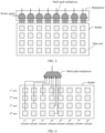
- FIG. 3 is a diagram of a buffer and a multiplexer according to an embodiment of this application.
- Each buffer includes W rows and K columns of data units, and each data unit is configured to buffer a value of one element. In FIG. 3 , that W is equal to 4 and K is equal to 8 is used as an example.
- Each buffer corresponds to K read ports, each read port is implemented as a multi-path multiplexer, and a multiplexer corresponding to one buffer includes K multi-path multiplexers.
- the first multiplexer 130 and the second multiplexer 150 in FIG. 1 separately include K multi-path multiplexers.
- Each multi-path multiplexer is connected to a plurality of data units in the buffer, and each data unit is connected to at least one multi-path multiplexer.
- Each multi-path multiplexer may be configured to read data buffered in the plurality of data units connected to the multi-path multiplexer.
- Each multi-path multiplexer can read data in only one data unit from the plurality of connected data units each time based on the selection signal of the scheduling module 160.
- FIG. 4 is a diagram in which a multi-path multiplexer is connected to the buffer according to an embodiment of this application.
- One multiplexer includes a plurality of multi-path multiplexers, each multi-path multiplexer is separately connected to the plurality of data units in the buffer, and the plurality of data units connected to one multi-path multiplexer have different priorities.
- a data unit in each buffer is represented as (r, c).
- a data unit in a 1 st row and a 3 rd column is represented as (1, 3)
- a data unit in a 4 th row and a 5 th column is represented as (4, 5), and the rest may be deduced by analogy.
- each multi-path multiplexer is connected to eight data units of the buffer, and priorities of the eight data units connected to an i th multi-path multiplexer are sequentially: (1, i), (2, i), (3, i), (4, i), (2, i+1), (2, mod (i-1, 8)), (3, mod (i-2, 8)), (4, mod (i-3, 8)) in descending order.
- mod is a modulo operation.
- FIG. 5 shows a priority sequence of eight data units separately connected to two multi-path multiplexers when i is equal to 1 (in other words, a 1 st multi-path multiplexer) and i is equal to 4 (in other words, a 4 th multi-path multiplexer).
- Digits 1 to 8 in the data units in FIG. 5 indicate priorities. A smaller digit indicates a higher priority.
- Priorities of eight data units connected to the 1 st multi-path multiplexer are sequentially: (1, 1), (2, 1), (3, 1), (4, 1), (2, 2), (2, 8), (3, 7), and (4, 6) in descending order.
- Priorities of eight data units connected to the 4 th multi-path multiplexer are sequentially: (1, 4), (2, 4), (3, 4), (4, 4), (2, 5), (2, 3), (3, 2) and (4, 1) in descending order.
- each multi-path multiplexer is connected to eight data units shown in FIG. 4 is merely an example, and cannot be understood as a specific limitation.
- Each multi-path multiplexer may be further connected to more or fewer data units.
- each multi-path multiplexer is connected to seven data units, or is connected to 10, 15, or 16 data units, provided that each data unit is connected to at least one multi-path multiplexer.
- a connection relationship between each multi-path multiplexer and the plurality of data units in FIG. 4 is merely an example, and cannot be understood as a specific limitation.
- the connection relationship between each multi-path multiplexer and the plurality of data units is not specifically limited in this application. However, in a same chip, each buffer needs to include W rows and K columns of data units.
- a buffer and a multiplexer connected to the buffer are referred to as a buffer module.
- connection relationships between multiplexers and data units in buffers in any two buffer modules in a same chip are the same.
- a connection relationship between a multi-path multiplexer in each buffer module and a data unit in a buffer is the same.
- a relative position, in the first buffer 120, of a plurality of data units connected to a 1 st multi-path multiplexer in the first multiplexer 130 are the same as a relative position, in the second buffer 140, of a plurality of data units connected to a 1 st multi-path multiplexer in the second multiplexer 150.
- an i th multi-path multiplexer in the first multiplexer 130 is connected to eight data units that are (1, i), (2, i), (3, i), (4, i), (2, i+1), (2, mod (i-1, 8)), (3, mod (i-2, 8)), and (4, mod (i-3, 8)) in the first buffer 120
- an i th multi-path multiplexer in the second multiplexer is also connected to eight data units that are (1, i), (2, i), (3, i), (4, i), (2, i+1), (2, mod (i-1, 8)), (3, mod (i-2, 8)), (4, mod (i-3, 8)) in the second buffer.
- the i th multi-path multiplexer in the first multiplexer and the i th multi-path multiplexer in the second multiplexer can read, based on a same selection signal, data in data units whose relative positions are the same in the first buffer 120 and the second buffer 140, and the first multiplexer and the second multiplexer read, based on the same selection signal, exactly elements that are multiplied in the first vector and the second vector.
- each multi-path multiplexer reads a non-zero element from a plurality of connected data units each time.
- the scheduling module 160 determines, based on priorities and starting from a data unit with a highest priority, whether an element in a data unit with a priority of 1 is 0.
- the scheduling module 160 If the element in the data unit with the priority of 1 is not 0, the scheduling module 160 generates a selection signal of the data unit with the priority of 1, so that the multi-path multiplexer reads the element in the data unit with the priority of 1; or if the element in the data unit with the priority of 1 is 0, the scheduling module 160 further determines whether an element in a data unit with a priority of 2 is 0. If the element in the data unit with the priority of 2 is not 0, the scheduling module 160 generates a selection signal of the data unit with the priority of 2, so that the multi-path multiplexer reads the element in the data unit with the priority of 2; or if the element in the data unit with the priority of 2 is 0, the scheduling module 160 further determines whether an element in a data unit with a priority of 3 is 0.
- the scheduling module 160 finds, in a priority sequence, a data unit whose stored element is not 0, and then generates a selection signal corresponding to the data unit, so that the multi-path multiplexer reads the element in the data unit and sends the element to the processing element 110, to cause the processing element 110 to perform a dot product operation.
- One buffer is connected to K multi-path multiplexers.
- each multi-path multiplexer needs to read one element from the buffer based on the selection signal of the scheduling module 160 and send the element to the processing element 110.
- the multiplexer can obtain K elements from the connected buffer by using the K multi-path multiplexers. It should be noted that, if elements in a plurality of data units connected to one multi-path multiplexer are all 0, the multi-path multiplexer sends the element 0 to the processing element 110.
- the scheduling module 160 determines, based on a bitmap (bitmap) corresponding to data stored the buffer, whether an element in each data unit is 0.
- FIG. 6 is a diagram of the data in the buffer and the corresponding bitmap. After storing data, each buffer generates a bitmap based on the data buffered in a data unit, and each bit in the bitmap corresponds to one data unit in the buffer. A value of each bit in the bitmap is 0 or 1, and indicates whether an element in a corresponding data unit is 0.
- bit in the bitmap when a bit in the bitmap is 0, it indicates that a value of an element in a data unit corresponding to the bit is 0, and when a bit in the bitmap is 1, it indicates that a value in a data unit corresponding to the bit is not 0.
- bit in the bitmap when a bit in the bitmap is 0, it indicates that a value in a data unit corresponding to the bit is not 0; and when a bit in the bitmap is 1, it indicates that a value in a data unit corresponding to the bit is 0.
- a bit in the bitmap is 0 indicates that a value in a data unit corresponding to the bit is 0, and a bit in the bitmap is 1 indicates that a value in a data unit corresponding to the bit is not 0 is used as an example to describe this embodiment of this application.
- the scheduling module 160 When the scheduling module 160 needs to generate a selection signal of a multi-path multiplexer, the scheduling module 160 first determines, whether a value of a bit corresponding to a data unit with a priority of 1 in data units connected to the multi-path multiplexer in the bitmap is 0. If the value of the bit corresponding to the data unit with the priority of 1 in the bitmap is 1, it indicates that an element in the data unit with the priority of 1 is not 0. The scheduling module 160 generates a selection signal corresponding to the data unit with the priority of 1, and sends the selection signal to the multi-path multiplexer. If the value of the bit corresponding to the data unit with the priority of 1 in the bitmap is 0, it indicates that an element in the data unit with the priority of 1 is 0.
- the scheduling module 160 further determines whether a value of a bit corresponding to a data unit with a priority of 2 in the data units connected to the multi-path multiplexer in the bitmap is 0. If the value of the bit corresponding to the data unit with the priority of 2 in the bitmap is 1, it indicates that an element in the data unit with the priority of 2 is not 0.
- the scheduling module generates a selection signal corresponding to the data unit with the priority of 2, and sends the selection signal to the multi-path multiplexer. If the value of the bit corresponding to the data unit with the priority of 2 in the bitmap is 0, it indicates that the element in the data unit with the priority of 2 is 0.
- the scheduling module 160 further determines whether a value of a bit corresponding to a data unit with a priority of 3 in the data units connected to the multi-path multiplexer in the bitmap is 0.
- the scheduling module 160 controls a multi-path multiplexer to obtain a non-zero element from a data unit
- the scheduling module 160 needs to set a corresponding position of the element stored in the data unit in the bitmap to 0, to prevent the element in the data unit from being repeatedly read, and avoid a computing error caused because a non-zero element in a data unit with a priority lower than the data unit is not read and does not participate in an operation.
- FIG. 2 to FIG. 6 describe working principles of parts included in the chip 100 shown in FIG. 1 .
- the following describes, with reference to the accompanying drawings, methods for implementing an operation between vectors, an operation between a vector and a matrix, and an operation between matrices by using the chip 100.
- FIG. 7 is a diagram of implementing an operation between vectors according to an embodiment of this application. That the chip 100 in FIG. 1 implements a dot product operation between a vector C and a vector D is used as an example.
- the first buffer 120 and the second buffer 140 in the chip 100 both include W rows and K columns of data units, and the first multiplexer 130 and the second multiplexer 150 both include K multi-path multiplexers.
- the vector C is a 1*WK vector
- the vector D is a WK*1 vector.
- the vector C includes one row and W*K columns of elements
- the vector D includes W*K rows and one column of elements.
- the chip 100 loads an element included in the vector C into a data unit in the first buffer 120, and loads an element included in the vector D into a data unit in the second buffer 140.
- data in the vector C is loaded into the first buffer 120 and data in the vector D is loaded into the second buffer 140
- data in a 1 st column to a K th column in the vector C is sequentially stored in K data units in a 1 st row in the first buffer 120
- data in a 1 st row to a K th row in the vector D is sequentially stored in K data units in a 1 st row in the second buffer 140.
- Data in a (K+1) th column to a 2K th column in the vector C is sequentially stored in K data units in a 2 nd row in the first buffer 120, and data in a (K+1) th row to a 2K th row in the vector D is sequentially stored in K data units in a 2 nd row in the second buffer 140.
- the rest may be deduced by analogy until data in a (W-1)K th column to a WK th column in the vector C is sequentially stored in K data units in a W th row in the first buffer 120, and data in a (W-1)K th row to a WK th row in the vector D is sequentially stored in K data units in a W th row in the second buffer 140.
- the first buffer 120 After W*K pieces of data in the vector C are stored in the first buffer 120, the first buffer 120 generates a corresponding bitmap based on a value of an element stored in each data unit. If a value of an element in a data unit is not 0, a corresponding bit of the data unit in the bitmap is set to 1; or if a value of an element in a data unit is 0, a corresponding bit of the data unit in the bitmap is set to 0. As shown in FIG. 6 , the bitmap shown in FIG. 6 is a bitmap corresponding to the data buffered by the first buffer 120. In FIG. 6 , that W is equal to 4 and K is equal to 8 is used as an example.
- FIG. 4 A connection relationship between each multi-path multiplexer in the first multiplexer 130 and a data unit in the first buffer 120 is shown in FIG. 4 . It should be understood that a corresponding bitmap based on a value in each data unit may alternatively be generated by the second buffer 140. This is not specifically limited in this embodiment of this application.
- the first buffer 120 After generating the bitmap, the first buffer 120 sends the bitmap to the scheduling module 160. After receiving the bitmap, the scheduling module 160 needs to first generate a selection signal DS 1 of the 1 st multi-path multiplexer in the first multiplexer 130. Specifically, the scheduling module 160 first determines, based on priorities of a plurality of data units connected to the 1 st multi-path multiplexer in the first multiplexer 130, whether a value of a bit corresponding to a data unit with a priority of 1 in the data units connected to the 1 st multi-path multiplexer in the first multiplexer 130 in the bitmap is 0.
- the scheduling module 160 If the value of the bit corresponding to the data unit with the priority of 1 in the bitmap is not 0, the scheduling module 160 generates a selection signal 000, and sends the selection signal 000 to the 1 st multi-path multiplexer in the first multiplexer 130 and the 1 st multi-path multiplexer in the second multiplexer 150.
- the selection signal 000 is used to cause the 1 st multi-path multiplexer in the first multiplexer 130 to read an element in the data unit with the priority of 1 and send the element to the processing element 110, and cause the 1 st multi-path multiplexer in the second multiplexer 150 to read the element in the data unit with the priority of 1 and send the element to the processing element 110.
- the scheduling module 160 determines that the value of the bit corresponding to the data unit with the priority of 1 in the data units connected to the 1 st multi-path multiplexer in the first multiplexer 130 in the bitmap is 0, the scheduling module 160 further determines whether a value of a bit corresponding to a data unit with a priority of 2 in the data units connected to the 1 st multi-path multiplexer in the first multiplexer 130 in the bitmap is 0.
- the scheduling module 160 If the value of the bit corresponding to the data unit with the priority of 2 in the bitmap is not 0, the scheduling module 160 generates a selection signal 001, and sends the selection signal 001 to the 1 st multi-path multiplexer in the first multiplexer 130 and the 1 st multi-path multiplexer in the second multiplexer 150.
- the selection signal 001 is used to cause the 1 st multi-path multiplexer in the first multiplexer 130 to read an element in the data unit with the priority of 2 and send the element to the processing element 110, and cause the 1 st multi-path multiplexer in the second multiplexer 150 to read the element in the data unit with the priority of 2 and send the element to the processing element 110.
- the scheduling module 160 determines that the value of the bit corresponding to the data unit with the priority of 2 in the data units connected to the 1 st multi-path multiplexer in the first multiplexer 130 in the bitmap is 0, the scheduling module 160 further determines whether a value of a bit corresponding to a data unit with a priority of 3 in the data units connected to the 1 st multi-path multiplexer in the first multiplexer 130 in the bitmap is 0.
- the rest may be deduced by analogy until the 1 st multi-path multiplexer in the first multiplexer 130 reads one piece of data c 1 from the first buffer 120 and sends the data c 1 to the processing element 110, and the 1 st multi-path multiplexer in the second multiplexer 150 reads one piece of data d 1 from the second buffer 140 and sends the data d 1 to the processing element 110, to cause the processing element 110 to perform an operation of c 1 *d 1 .
- a value of c 1 is not 0, and d 1 may be 0 or may not be 0. If all data buffered by the plurality of data units connected to the 1 st multi-path multiplexer in the first multiplexer 130 is 0, the value of c 1 is 0, and d 1 may be 0 or may not be 0.
- the scheduling module 160 sequentially generates corresponding selection signals DS 2 to DS K through a same method, so that each multi-path multiplexer in the first multiplexer 130 and the second multiplexer 150 outputs one piece of data to the processing element 110.
- each multi-path multiplexer in the first multiplexer 130 and the second multiplexer 150 outputs one piece of data to the processing element 110, so that the processing element 110 completes K times of product operations and K-1 times of addition operations.
- the scheduling module 160 After the scheduling module 160 generates a selection signal and sends the selection signal to the first multiplexer 130, and the first multiplexer 130 reads one piece of data from a data unit, the scheduling module 160 sets a corresponding position of the data unit in the bitmap to 0.
- the scheduling module 160 continues to perform operations performed in the first periodicity, so that each multi-path multiplexer in the first multiplexer 130 and the second multiplexer 150 outputs one piece of data to the processing element 110, and the processing element 110 completes K times of product operations and K-1 times of addition operations, until values of all bits in the bitmap are all 0. Finally, values obtained after the processing element 110 completes K times of product operations and K-1 times of addition operations in each periodicity are added, and a dot product of the vector C and the vector D is obtained.
- the scheduling module 160 determines that all values in the bitmap are 0, the scheduling module 160 generates an erasing signal, and sends the erasing signal to the first buffer 120 and the second buffer 140, so that the first buffer 120 and the second buffer 140 erase currently buffered data, to help buffer a next batch of data.
- the vector C may be a part of a vector X
- the vector D may be a part of a vector Y
- the vector X is a 1 *Z vector
- the vector Y is a Z*1 vector, where Z is greater than W*K.
- the vector C may be a row vector with one row and W*K columns
- the vector D may be any column in a matrix with W*K rows and T columns
- an operation result of the vector C and the matrix is a vector with one row and T columns.
- one column in the matrix is buffered in the second buffer 140 each time, to obtain an element in the operation result.
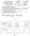
- FIG. 8 is a diagram of another chip according to an embodiment of this application.
- a chip 200 includes N processing elements PE 1 to PE N , N+1 buffers B 0 to B N , N+1 multiplexers M 0 to M N , and a scheduling module 210.
- N is an integer greater than or equal to 2.
- the buffer B 0 is connected to the scheduling module 210, the scheduling module 210 is connected to each multiplexer, the N+1 buffers are in one-to-one correspondence with the N+1 multiplexers, and each multiplexer is connected to one buffer.
- the multiplexer M 0 is connected to all the N processing elements, and data read by the multiplexer M 0 each time is synchronously sent to the N processing elements.
- For a connection relationship between each multiplexer and a corresponding buffer refer to the descriptions corresponding to FIG. 3 and FIG. 4 . Details are not described herein again.
- the chip 200 can implement a multiplication operation between a vector and a matrix. That the chip 200 shown in FIG. 8 implements a multiplication operation between a vector C and a matrix B is used as an example. Buffers in the chip 200 all include W rows and K columns of data units, and multiplexers all include K multi-path multiplexers.
- the vector C is a 1*WK vector
- the matrix B is a WK*N matrix. In other words, the vector C includes one row and W*K columns of elements, and the matrix B includes W*K rows and N columns of elements. It should be understood that the matrix B is equivalent to N WK* 1 vectors, in other words, the matrix B is equivalent to N vectors D.
- the multiplication operation between the vector C and the matrix B is equivalent to performing a dot product operation between vectors between the vector C and each column in the matrix B. Therefore, the matrix B may be considered as N vectors including vectors D 1 to D N , and each vector corresponds to a column in the matrix B.
- FIG. 9 is a diagram of implementing the operation between a vector and a matrix according to an embodiment of this application. Black squares in the vector C and the matrix B in FIG. 9 represent non-zero elements.
- the chip 200 loads an element included in the vector C into a data unit in the buffer B 0 , loads an element in a vector D 1 corresponding to a 1 st column in the matrix B into a data unit in a buffer B 1 , loads an element in a vector D 2 corresponding to a 2 nd column in the matrix B into a data unit in a buffer B 2 , and loads an element included in a vector D 3 corresponding to a 3 rd column in the matrix B into a data unit in a buffer B 3 .
- an element in a vector D N corresponding to an N h column in the matrix B is loaded into a data unit in the buffer B N .
- a method for loading the vector C into the buffer B 0 refer to the method for loading the vector C into the first buffer 120 in the embodiment corresponding to FIG. 7 .
- a method for loading the vectors D 1 to D N into corresponding buffers refer to the method for loading the vector D into the second buffer 140 in the embodiment corresponding to FIG. 7 . Details are not described herein again.
- the buffer B 0 After WK pieces of data in the vector C are stored in the buffer B 0 , the buffer B 0 generates a corresponding bitmap. For a method for generating the corresponding bitmap by the buffer B 0 , refer to the method for generating the bitmap by the first buffer 120. Details are not described herein again.
- the buffer B 0 After generating the bitmap, the buffer B 0 sends the bitmap to the scheduling module 210.
- the scheduling module 210 After receiving the bitmap, the scheduling module 210 first generates a selection signal DS 1 of a 1 st multi-path multiplexer in the multiplexer M 0 . For a method for generating the selection signal DS 1 by the scheduling module 210, refer to the method for generating the selection signal DS 1 by the scheduling module 160. Details are not described herein again.
- the scheduling module 210 sends the selection signal DS 1 to 1 st multi-path multiplexers in the multiplexers M 0 to M N .
- the 1 st multi-path multiplexer in the multiplexer M 0 reads one piece of data based on the selection signal DS 1 , and sends the data to N processing elements PE 0 to PE N .
- 1 st multi-path multiplexers in multiplexers M 1 to M N each read one piece of data based on the selection signal DS 1 , and send the data to processing elements connected to the multiplexers.
- the scheduling module 210 For a 2 nd to a K th multi-path multiplexers in the multiplexers M 0 to M N , the scheduling module 210 sequentially generates corresponding selection signals DS 2 to DS K through a same method, so that each multi-path multiplexer in the multiplexers M 0 to M N outputs one piece of data to the processing element PE 1 to PE N . After the scheduling module 210 sequentially generates selection signals DS 1 to DS K in one periodicity, each processing element obtains K pairs of data, and completes K times of product operations and K-1 times of addition operations.
- the scheduling module 210 After the scheduling module 210 generates a selection signal and sends the selection signal to the multiplexer M 0 , and the multiplexer M 0 reads one piece of data from a data unit, the scheduling module 210 sets a corresponding position of the data unit in the bitmap to 0.
- the scheduling module 210 continues to perform operations performed in the first periodicity, so that each multi-path multiplexer in the multiplexers M 0 to M N outputs one piece of data to the processing element PE 1 to PE N , and the processing element PE 1 to PE N completes K times of product operations and K-1 times of addition operations, until values of all bits in the bitmap are all 0.
- values obtained after K times of product operations and K-1 times of addition operations are completed in each periodicity are added, that is, a dot product of the vector C and a vector D h .
- h is a positive integer greater than or equal to 1 and less than or equal to N.
- a multiplication operation result of the vector C and the matrix B is a 1*N vector H.
- a value output by the processing element PE h after the dot product operation between the vector C and the vector D h is completed is a value of an h th element in the vector H.
- the vector C may be a part of a vector X, or may be a part or all of elements in a row in a matrix E.
- the matrix B may be a part of a matrix F.
- the vector X is a 1*Z vector
- the matrix F is a Z*N vector, where Z is greater than W*K. Because one buffer in the chip 200 can store only W*K pieces of data each time, the vector X and the matrix F are segmented, W*K elements in the vector X are stored in the buffer B 0 of the chip 200 each time, and W*K elements in an h th column in the matrix F are stored in a buffer B h of the chip 200. In other words, W*K elements in a 1 st column to an N h column in the matrix F are distributed and stored in the buffers B 0 to B N of the chip 200.
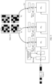
- FIG. 10 is a diagram of another chip according to an embodiment of this application.
- a chip 300 includes M*N processing elements PEs, M+N buffers, M*(N+1) multiplexers, and M scheduling modules S 1 to S M .
- a connection relationship between parts included in the chip 300 is shown in FIG. 10 .
- the M*N processing elements are distributed in a matrix manner, the M*N processing elements are distributed in M rows, and each row includes N processing elements.
- Each row in a structure of the chip 300 in FIG. 10 is equivalent to a structure of the chip 200 shown in FIG. 8
- the chip 300 is equivalent to a chip including M chips 200 shown in FIG. 8 .
- the chip 300 can implement a multiplication operation between matrices. That the chip 300 shown in FIG. 10 implements a multiplication operation between a matrix A and a matrix B is used as an example.
- Each buffer in the chip 300 includes W rows and K columns of data units, and each multiplexer includes K multi-path multiplexers.
- the matrix A is an M*WK matrix
- the matrix B is a WK*N matrix.
- the matrix A includes M rows and W*K columns of elements
- the matrix B includes W*K rows and N columns of elements. It should be understood that the matrix A is equivalent to M 1*WK vectors, in other words, the matrix A is equivalent to M vectors C.
- the multiplication operation between the matrix A and the matrix B is equivalent to performing a multiplication operation between a vector and a matrix between each row in the matrix A and the matrix B. Therefore, the matrix A may be considered as M vectors including vectors C 1 to C M , and each vector corresponds to a row in the matrix A.
- FIG. 11 is a diagram of implementing the operation between matrices according to an embodiment of this application.
- the chip 300 can simultaneously compute a multiplication operation between M vectors and the matrix B through a method for computing the multiplication operation between the vector C and the matrix B by the chip 200.
- the chip 300 can compute a multiplication operation between the matrix B and the M vectors (vectors C 1 to C M ) included in the matrix A, to obtain a multiplication operation result of the matrix A and the matrix B.
- the matrix A is an M*WK matrix
- the matrix B is a WK*N matrix
- the multiplication operation result of the matrix A and the matrix B is an M*N matrix Q.
- a 1*N vector output by the N processing elements in a g th row in the chip 300 after a multiplication operation between a vector C g and the matrix B is completed is an element in a g th row in the matrix Q, where g is a positive integer greater than or equal to 1 and less than or equal to M.
- each buffer in buffers B 10 , B 20 , ..., B g0 , ..., B M0 in the chip 300 generates a bitmap corresponding to data buffered by each buffer, and sends the bitmap to a scheduling module connected to each buffer.
- B 10 generates a bitmap 1 and sends the bitmap 1 to the scheduling module S 1
- B 20 generates a bitmap 2 and sends the bitmap 2 to the scheduling module S 2
- B g0 generates a bitmap 1 and sends the bitmap 1 to the scheduling module S g , and the like.
- the matrix A may be a part of a matrix G
- the matrix B may be a part of a matrix F.
- the matrix A is an M*Z vector
- the matrix F is a Z*N vector, where Z is greater than W*K. Because one buffer in the chip 300 can store only W*K pieces of data each time, the matrix G and the matrix F are segmented, W*K elements in a g th row in the matrix G are stored in the buffer B g0 of the chip 300 each time, and W*K elements in an h th column in the matrix F are stored in a buffer B 1h of the chip 200.
- an element whose element value is 0 in the matrix may not participate in computing, to reduce a computing amount, improve computing efficiency without reducing computing precision.
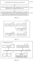
- FIG. 12 is a schematic flowchart of a matrix computing method according to an embodiment of this application.
- the matrix computing method includes the following S121 to S123.
- S121 A chip buffers a first vector and a second vector.
- the chip may be the chip 100 in FIG. 1 .
- the chip 100 buffers the first vector in a first buffer, and buffers the second vector in a second buffer.
- a method for buffering the first vector in the first buffer by the chip 100 refer to the method for buffering the vector C in the first buffer 120 by the chip 100.
- a method for buffering the second vector in the second buffer refer to the method for buffering the vector D in the second buffer 140 by the chip 100. Details are not described herein again.
- the first vector may be the vector C in the embodiment shown in FIG. 7
- the second vector may be the vector D in the embodiment shown in FIG. 7
- the first vector may be a part of a vector X
- the second vector may be a part of a vector Y
- the vector X is a 1*Z vector
- the vector Y is a Z*1 vector, where Z is greater than W*K. Because one buffer in the chip 100 can store only W*K pieces of data each time, the vector X and the vector Y are segmented, and a maximum of W*K elements are stored in the buffer of the chip 100 for computing each time.
- the first vector may be a row in a first matrix or a part of elements in a row in the first matrix
- the second vector may be a column in a second matrix or a part of elements in a column in the second matrix.
- the vector X is a row in the first matrix
- the vector Y is a column in the second matrix.
- a first scheduling module of the chip generates a first selection signal based on a bitmap of the first vector.
- the bitmap of the first vector indicates a non-zero element in the first vector.
- the first selection signal may cause a first processing element to obtain, from the first buffer, a first group of non-zero elements in the first vector, and cause the first processing element to obtain, from the second buffer, a second group of elements in the second vector.
- the second group of elements obtained from the second vector may include a non-zero element, or may be all zero elements.
- the chip 100 further includes a first multiplexer and a second multiplexer.
- the first processing element obtains, from the first buffer, the first group of non-zero elements in the first vector by using the first multiplexer, and obtains, from the second buffer, the second group of non-zero elements in the second vector by using the second multiplexer.
- the first scheduling module may be the scheduling module 160 in FIG. 7
- the first multiplexer may be the first multiplexer 130 in FIG. 7
- the second multiplexer may be the second multiplexer 150 in FIG. 7 .
- the first selection signal is the selection signals DS 1 to DS K in the embodiment corresponding to FIG. 7 .
- the first scheduling module For a process in which the first scheduling module generates the first selection signal based on the bitmap of the first vector, refer to a process in which the scheduling module 160 generates the selection signals DS 1 to DS K based on the bitmap of the vector C in the embodiment corresponding to FIG. 7 . Details are not described herein again.
- the first processing element of the chip implements an operation between the first vector and the second vector based on the first group of non-zero elements and the second group of elements.
- the first processing element may be the processing element 110 in FIG. 7 .
- the first group of non-zero elements are K pieces of data that are obtained by K multi-path multiplexers in the first multiplexer from the first buffer based on a received selection signal.
- the second group of elements are K pieces of data that are obtained by K multi-path multiplexers in the second multiplexer from the second buffer based on a received selection signal.
- the chip may further include a third buffer and a second processing element.
- the third buffer is configured to buffer a third vector.
- the first selection signal may further cause the second processing element to obtain, from the third buffer, a third group of elements in the third vector, and cause the second processing element to obtain, from the first buffer, the first group of non-zero elements in the first vector.
- the second processing element implements an operation between the first vector and the third vector based on the first group of non-zero elements in the first vector and the third group of elements in the third vector.
- the third vector belongs to a column in the second matrix other than a column in which the second vector is located.
- the first buffer may be the buffer B 0 in FIG. 8
- the second buffer may be the buffer B 1 in FIG. 8
- the first multiplexer may be the multiplexer M 0 in FIG. 8
- the second multiplexer may be the multiplexer M 1 in FIG. 8
- the first processing element may be the processing element PE 1 in FIG. 8
- the third buffer may be any one or more of the buffers B 2 to B N in FIG. 8 .
- the second processing element is a processing element connected to the third buffer
- the third multiplexer is a multiplexer connected to the third buffer.
- the chip when the chip includes the third buffer and the second processing element, the chip may be the chip 200 shown in FIG. 8 .
- the chip may further include a fourth buffer, a second scheduling module, and a third processing element.
- the fourth buffer is configured to buffer a fourth vector, where the fourth vector belongs to a row in the first matrix other than a row in which the first vector is located.
- the second scheduling module generates a second selection signal based on a bitmap of the fourth vector.
- the second selection signal may cause the third processing element to obtain, from the fourth buffer, a fourth group of non-zero elements in the fourth vector, and cause the third processing element to obtain, from the second buffer, a fifth group of elements in the second vector.
- the second processing element can implement an operation between the fourth vector and the second vector based on the fourth group of non-zero elements in the fourth vector and the fifth group of elements in the second vector.
- the bitmap of the fourth vector indicates a non-zero element in the fourth vector.
- the first buffer may be a buffer B 10 in FIG. 10
- the second buffer may be a buffer B 11 in FIG. 10
- the first multiplexer may be a multiplexer M 10 in FIG. 10
- the second multiplexer may be a multiplexer M 11 in FIG. 10
- the first processing element may be a processing element PE 11 in FIG. 10
- the third buffer may be any one or more of buffers B 12 to B 1N in FIG. 10
- the second processing element is a processing element connected to the third buffer
- the third multiplexer is a multiplexer connected to the third buffer.
- the second scheduling module may be any one or more of the scheduling modules S 2 to S M in FIG. 10 .
- the fourth buffer is a buffer connected to the second scheduling module
- the third processing element is one or more processing elements in a same row as the second scheduling module in FIG. 10 .
- the chip when the chip further includes the fourth buffer, the second scheduling module, and the third processing element in addition to the first buffer, the second buffer, the first scheduling module, the first processing element, the third buffer, and the second processing element, the chip may be the chip 300 shown in FIG. 10 .
- the chip 300 For methods for implementing operations on the first vector and the second vector, the first vector and the third vector, and the fourth vector and the second vector by the chip 300, refer to related descriptions in embodiments corresponding to FIG. 10 and FIG. 11 . Details are not described herein again.
- FIG. 13 is a diagram of a matrix computing apparatus according to an embodiment of this application.
- the matrix computing apparatus may be the foregoing chip 100, the chip 200, or the chip 300.
- a matrix computing apparatus 131 includes a first scheduling unit 132 and a first processing unit 133.
- the first scheduling unit 132 is configured to generate a first selection signal based on a bitmap of a first vector.
- the first selection signal may cause the first processing unit 133 to obtain, from a first buffer, a first group of non-zero elements in the first vector, and cause the first processing unit 133 to obtain, from a second buffer, a second group of elements in a second vector.
- the first processing unit 133 is configured to implement an operation between the first vector and the second vector based on the first group of non-zero elements in the first vector and the second group of elements in the second vector, and the bitmap of the first vector indicates a non-zero element in the first vector.
- the matrix computing apparatus 131 may be the chip 100 shown in FIG. 7 .
- the first scheduling unit 132 may be configured to implement a function implemented by the scheduling module 160, and the first processing unit 133 may be configured to implement a function implemented by the processing element 110. Details are not described herein again.
- the first scheduling unit 132 After the first processing unit 133 implements the operation between the first vector and the second vector based on the first group of non-zero elements and the second group of elements, the first scheduling unit 132 generates an erasing signal, where the erasing signal indicates the first buffer and the second buffer to erase currently buffered data.
- the first vector belongs to a part or all of elements in any row in a first matrix
- the second vector belongs to a part or all of elements in any column in a second matrix
- the matrix computing apparatus further includes a second processing unit 134
- the first selection signal may further cause the second processing unit 134 to obtain a third group of elements in a third vector, and cause the second processing unit 134 to obtain the first group of non-zero elements in the first vector.
- the second processing unit 134 is configured to implement an operation between the first vector and the third vector based on the first group of non-zero elements and the third group of elements.
- the third vector belongs to a column in the second matrix other than a column in which the second vector is located.
- the matrix computing apparatus 131 may be the chip 200 shown in FIG. 8 or FIG. 9 .
- the first scheduling unit 132 may be configured to implement a function implemented by the scheduling module 210 in FIG. 9 .
- the first processing unit 133 may be configured to implement a function implemented by the processing element PE 1 in FIG. 9 .
- the second processing unit 134 is configured to implement a function implemented by a processing element other than the processing element PE 1 in FIG. 9 . Details are not described herein again.
- the matrix computing apparatus further includes a second scheduling unit 135 and a third processing unit 136.
- the second scheduling unit 135 generates a second selection signal based on a bitmap of a fourth vector.
- the second selection signal is used to cause the third processing unit 136 to obtain a fourth group of non-zero elements in the fourth vector, and cause the third processing unit 136 to obtain a fifth group of elements in the second vector.
- the bitmap of the fourth vector indicates a non-zero element in the fourth vector.
- the third processing unit 136 is configured to implement an operation between the fourth vector and the second vector based on the fourth group of non-zero elements and the fifth group of elements.
- the matrix computing apparatus 131 may be the chip 300 shown in FIG. 10 or FIG. 11 .
- the first scheduling unit 132 may be configured to implement a function implemented by the scheduling module S 1 in FIG. 11
- the first processing unit 133 may be configured to implement a function implemented by the processing element PE 11 in FIG. 11 .
- the second processing unit 134 is configured to implement a function implemented by a processing element other than the processing element PE 11 in a 1 st row in FIG. 11
- the first scheduling unit 132 may be configured to implement a function implemented by a scheduling module other than the scheduling module S 1 in FIG. 11 . Details are not described herein again.
- FIG. 14 is a diagram of a computing device according to an embodiment of this application.
- a computing device 141 includes the foregoing chip 100, chip 200, or chip 300.
- the computing device 141 further includes a processor 142, a chip 143, a memory 144, and a communication interface 145.
- the processor 142, the memory 144, and the communication interface 145 communicate with each other via a bus 146.
- the chip 143 may be any one of the chip 100, the chip 200, or the chip 300, and can assist the computing device 141 in implementing various functions implemented by the chip 100, the chip 200, or the chip 300.
- the chip 143 can implement, under scheduling of the processor 142, the operations in embodiments corresponding to FIG. 7 to FIG. 12 .
- the processor 142 may have a plurality of specific implementation forms.
- the processor 142 may be a central processing unit (central processing unit, CPU), a graphics processing unit (graphics processing unit, GPU), an embedded neural-network processing unit (neural-network processing unit, NPU), or a tensor processing unit (tensor processing unit, TPU), or the processor 142 may be a single-core processor or a multi-core processor.
- the processor 142 may be a combination of a CPU and a hardware chip.
- the hardware chip may be an ASIC, a programmable logic device (programmable logic device, PLD), or a combination thereof.
- the PLD may be a complex programmable logic device (complex programmable logic device, CPLD), a field-programmable logic gate array (field-programmable gate array, FPGA), a generic array logic (generic array logic, GAL), or any combination thereof.
- the processor 142 may alternatively be implemented independently by using a logic device with built-in processing logic, for example, an FPGA or a digital signal processor (digital signal processor, DSP).
- the memory 144 may be a nonvolatile memory, for example, a read-only memory (read-only memory, ROM), a programmable read-only memory (programmable ROM, PROM), an erasable programmable read-only memory (erasable PROM, EPROM), an electrically erasable programmable read-only memory (electrically EPROM, EEPROM), or a flash memory.
- the memory 144 may alternatively be a volatile memory.
- the volatile memory may be a random access memory (random access memory, RAM), and is used as an external cache.
- the memory 144 may be configured to store program code and data, for example, buffer the foregoing vector or matrix, so that the chip 143 invokes the program code stored in the memory 144 to perform the operation steps in embodiments corresponding to FIG. 1 to FIG. 12 .
- the communication interface 145 may be a wired interface (for example, an Ethernet interface), an internal interface (for example, a peripheral component interconnect express (Peripheral Component Interconnect express, PCIE) bus interface), a wired interface (for example, an Ethernet interface), or a wireless interface (for example, a cellular network interface or a wireless local area network interface).
- the communication interface 145 is configured to communicate with another computing device or module.
- the bus 146 is a peripheral component interconnect express (Peripheral Component Interconnect Express, PCIE) bus, an extended industry standard architecture (extended industry standard architecture, EISA) bus, a unified bus (unified bus, U bus, or UB), a compute express link (compute express link, CXL), a cache coherent interconnect for accelerators (cache coherent interconnect for accelerators, CCIX) bus, or the like.
- PCIE peripheral component interconnect express
- EISA extended industry standard architecture
- unified bus unified bus, U bus, or UB
- CXL compute express link
- cache coherent interconnect for accelerators cache coherent interconnect for accelerators
- the bus 146 includes an out-of-band bus, a high-speed bus, and the like. For clear description, various buses are marked as the bus 146 in the figure.
- FIG. 14 is only a possible implementation of this embodiment of this application.
- the computing device 141 may alternatively include more or fewer components. This is not limited herein.
- An embodiment of this application provides a computer-readable storage medium.
- the computer-readable storage medium stores computer instructions.
- the computing device is caused to perform the operations in embodiments corresponding to FIG. 1 to FIG. 12 .
- An embodiment of this application provides a computer program product including instructions, including a computer program or instructions.
- the computing device is caused to perform the operations in embodiments corresponding to FIG. 1 to FIG. 12 .
- All or a part of the foregoing embodiments may be implemented by software, hardware, firmware, or any combination thereof.
- all or a part of the foregoing embodiments may be implemented in a form of a computer program product.
- the computer program product includes at least one computer instruction.
- the computer program instruction is loaded or executed on a computer, procedure or functions according to embodiments of this application are all or partially generated.
- the computer is a general-purpose computer, a dedicated computer, a computer network, or another programmable apparatus.
- the computer instruction may be stored in a computer-readable storage medium, or may be transmitted from a computer-readable storage medium to another computer-readable storage medium.
- the computer instruction is transmitted from a website, computer, server, or data center to another website, computer, server, or data center in a wired (for example, a coaxial cable, an optical fiber, or a digital subscriber line (digital subscriber line, DSL)) or wireless (for example, infrared, radio, or microwave) manner.
- the computer-readable storage medium may be any usable medium accessible by the computer, or a data storage node, such as a server or a data center that integrates at least one usable medium.
- the usable medium may be a magnetic medium (for example, a floppy disk, a hard disk drive, or a magnetic tape), an optical medium (for example, a high density digital video disc (digital video disc, DVD)), or a semiconductor medium.
Landscapes
- Engineering & Computer Science (AREA)
- Physics & Mathematics (AREA)
- Theoretical Computer Science (AREA)
- General Physics & Mathematics (AREA)
- General Engineering & Computer Science (AREA)
- Mathematical Physics (AREA)
- Software Systems (AREA)
- Mathematical Optimization (AREA)
- Pure & Applied Mathematics (AREA)
- Mathematical Analysis (AREA)
- Computational Mathematics (AREA)
- Data Mining & Analysis (AREA)
- Computing Systems (AREA)
- Algebra (AREA)
- Databases & Information Systems (AREA)
- Human Computer Interaction (AREA)
- Complex Calculations (AREA)
Applications Claiming Priority (3)
| Application Number | Priority Date | Filing Date | Title |
|---|---|---|---|
| CN202111567014 | 2021-12-20 | ||
| CN202210460849.1A CN116304509A (zh) | 2021-12-20 | 2022-04-28 | 一种矩阵计算方法、芯片以及相关设备 |
| PCT/CN2022/137086 WO2023116431A1 (zh) | 2021-12-20 | 2022-12-07 | 一种矩阵计算方法、芯片以及相关设备 |
Publications (2)
| Publication Number | Publication Date |
|---|---|
| EP4435637A1 true EP4435637A1 (de) | 2024-09-25 |
| EP4435637A4 EP4435637A4 (de) | 2025-03-19 |
Family
ID=86831052
Family Applications (1)
| Application Number | Title | Priority Date | Filing Date |
|---|---|---|---|
| EP22909746.4A Pending EP4435637A4 (de) | 2021-12-20 | 2022-12-07 | Matrixberechnungsverfahren, chip und zugehörige vorrichtung |
Country Status (4)
| Country | Link |
|---|---|
| US (1) | US20240338174A1 (de) |
| EP (1) | EP4435637A4 (de) |
| CN (2) | CN119166967A (de) |
| WO (1) | WO2023116431A1 (de) |
Family Cites Families (9)
| Publication number | Priority date | Publication date | Assignee | Title |
|---|---|---|---|---|
| GB2476800A (en) * | 2010-01-07 | 2011-07-13 | Linear Algebra Technologies Ltd | Sparse matrix vector multiplier using a bit map of non-zero elements to control scheduling of arithmetic operations |
| US10620951B2 (en) * | 2018-06-22 | 2020-04-14 | Intel Corporation | Matrix multiplication acceleration of sparse matrices using column folding and squeezing |
| CN110147347B (zh) * | 2019-03-18 | 2023-01-06 | 腾讯科技(深圳)有限公司 | 用于矩阵处理的芯片、矩阵处理方法、装置及存储介质 |
| US11120101B2 (en) * | 2019-09-27 | 2021-09-14 | Arm Limited | Matrix multiplication system and method |
| US11586601B2 (en) * | 2020-02-05 | 2023-02-21 | Alibaba Group Holding Limited | Apparatus and method for representation of a sparse matrix in a neural network |
| US11804851B2 (en) * | 2020-03-27 | 2023-10-31 | Intel Corporation | Methods, systems, articles of manufacture, and apparatus to decode zero-value-compression data vectors |
| CN113486298B (zh) * | 2021-06-28 | 2023-10-17 | 南京大学 | 基于Transformer神经网络的模型压缩方法、矩阵乘法模块 |
| CN113506589B (zh) * | 2021-06-28 | 2022-04-26 | 华中科技大学 | 一种稀疏矩阵存算系统及方法 |
| CN113721982B (zh) * | 2021-08-03 | 2025-08-26 | 清华大学 | 稀疏矩阵存储方法、向量计算方法和电子设备 |
-
2022
- 2022-04-28 CN CN202411124842.8A patent/CN119166967A/zh active Pending
- 2022-04-28 CN CN202210460849.1A patent/CN116304509A/zh active Pending
- 2022-12-07 EP EP22909746.4A patent/EP4435637A4/de active Pending
- 2022-12-07 WO PCT/CN2022/137086 patent/WO2023116431A1/zh not_active Ceased
-
2024
- 2024-06-20 US US18/748,393 patent/US20240338174A1/en active Pending
Also Published As
| Publication number | Publication date |
|---|---|
| CN119166967A (zh) | 2024-12-20 |
| CN116304509A (zh) | 2023-06-23 |
| WO2023116431A1 (zh) | 2023-06-29 |
| EP4435637A4 (de) | 2025-03-19 |
| US20240338174A1 (en) | 2024-10-10 |
Similar Documents
| Publication | Publication Date | Title |
|---|---|---|
| US11720646B2 (en) | Operation accelerator | |
| CN107689948B (zh) | 应用于神经网络硬件加速系统的高效数据访存管理装置 | |
| US20230026006A1 (en) | Convolution computation engine, artificial intelligence chip, and data processing method | |
| EP3553673A1 (de) | Faltungsoperationschip und kommunikationsvorrichtung | |
| CN112836813B (zh) | 一种用于混合精度神经网络计算的可重构脉动阵列系统 | |
| US20250173398A1 (en) | Matrix computing method and apparatus | |
| WO2021232422A1 (zh) | 神经网络的运算装置及其控制方法 | |
| CN111626405A (zh) | 一种cnn加速方法、加速装置及计算机可读存储介质 | |
| Bai et al. | A unified hardware architecture for convolutions and deconvolutions in CNN | |
| WO2021128820A1 (zh) | 数据处理方法、装置、设备、存储介质和程序产品 | |
| Wu et al. | Skeletongcn: a simple yet effective accelerator for gcn training | |
| US20200034699A1 (en) | Accelerating appratus of neural network and operating method thereof | |
| Shu et al. | High energy efficiency FPGA-based accelerator for convolutional neural networks using weight combination | |
| EP4435637A1 (de) | Matrixberechnungsverfahren, chip und zugehörige vorrichtung | |
| CN113516235A (zh) | 一种可变形卷积加速器和可变形卷积加速方法 | |
| CN109522125B (zh) | 一种矩阵乘积转置的加速方法、装置及处理器 | |
| US11663490B1 (en) | Partial sum pre-computation to implement quantized neural networks on programmable devices | |
| CN114647818A (zh) | 矩阵运算结果的确定方法及装置、存储介质、电子装置 | |
| WO2024199542A1 (zh) | 脉冲神经网络加速器、脉冲神经网络计算方法和计算设备 | |
| US20250173131A1 (en) | Application Acceleration Method and Apparatus, and Related Device | |
| CN113204372A (zh) | 存储受限型哈希算法的加速装置及方法 | |
| CN116992932A (zh) | 一种数据片外分块传输的参数化lstm加速系统及其设计方法 | |
| CN117332809A (zh) | 神经网络推理芯片、方法及终端设备 | |
| CN119761434A (zh) | 一种神经网络矩阵乘法加速器及其部署方法 | |
| CN117852655B (zh) | 利用大模型进行推理的方法和电子设备 |
Legal Events
| Date | Code | Title | Description |
|---|---|---|---|
| STAA | Information on the status of an ep patent application or granted ep patent |
Free format text: STATUS: THE INTERNATIONAL PUBLICATION HAS BEEN MADE |
|
| PUAI | Public reference made under article 153(3) epc to a published international application that has entered the european phase |
Free format text: ORIGINAL CODE: 0009012 |
|
| STAA | Information on the status of an ep patent application or granted ep patent |
Free format text: STATUS: REQUEST FOR EXAMINATION WAS MADE |
|
| 17P | Request for examination filed |
Effective date: 20240618 |
|
| AK | Designated contracting states |
Kind code of ref document: A1 Designated state(s): AL AT BE BG CH CY CZ DE DK EE ES FI FR GB GR HR HU IE IS IT LI LT LU LV MC ME MK MT NL NO PL PT RO RS SE SI SK SM TR |
|
| REG | Reference to a national code |
Ref country code: DE Ref legal event code: R079 Free format text: PREVIOUS MAIN CLASS: G06F0017160000 Ipc: G06F0003060000 |
|
| A4 | Supplementary search report drawn up and despatched |
Effective date: 20250218 |
|
| RIC1 | Information provided on ipc code assigned before grant |
Ipc: G06F 7/544 20060101ALN20250212BHEP Ipc: G06F 17/16 20060101ALI20250212BHEP Ipc: G06F 3/06 20060101AFI20250212BHEP |
|
| DAV | Request for validation of the european patent (deleted) | ||
| DAX | Request for extension of the european patent (deleted) |