EP4435554A1 - Reference voltage circuit - Google Patents
Reference voltage circuit Download PDFInfo
- Publication number
- EP4435554A1 EP4435554A1 EP23164072.3A EP23164072A EP4435554A1 EP 4435554 A1 EP4435554 A1 EP 4435554A1 EP 23164072 A EP23164072 A EP 23164072A EP 4435554 A1 EP4435554 A1 EP 4435554A1
- Authority
- EP
- European Patent Office
- Prior art keywords
- type mosfet
- depletion
- reference voltage
- depletion type
- electrode
- Prior art date
- Legal status (The legal status is an assumption and is not a legal conclusion. Google has not performed a legal analysis and makes no representation as to the accuracy of the status listed.)
- Pending
Links
Images




Classifications
-
- G—PHYSICS
- G05—CONTROLLING; REGULATING
- G05F—SYSTEMS FOR REGULATING ELECTRIC OR MAGNETIC VARIABLES
- G05F1/00—Automatic systems in which deviations of an electric quantity from one or more predetermined values are detected at the output of the system and fed back to a device within the system to restore the detected quantity to its predetermined value or values, i.e. retroactive systems
- G05F1/10—Regulating voltage or current
- G05F1/46—Regulating voltage or current wherein the variable actually regulated by the final control device is DC
- G05F1/56—Regulating voltage or current wherein the variable actually regulated by the final control device is DC using semiconductor devices in series with the load as final control devices
- G05F1/565—Regulating voltage or current wherein the variable actually regulated by the final control device is DC using semiconductor devices in series with the load as final control devices sensing a condition of the system or its load in addition to means responsive to deviations in the output of the system, e.g. current, voltage, power factor
- G05F1/567—Regulating voltage or current wherein the variable actually regulated by the final control device is DC using semiconductor devices in series with the load as final control devices sensing a condition of the system or its load in addition to means responsive to deviations in the output of the system, e.g. current, voltage, power factor for temperature compensation
-
- H—ELECTRICITY
- H10—SEMICONDUCTOR DEVICES; ELECTRIC SOLID-STATE DEVICES NOT OTHERWISE PROVIDED FOR
- H10D—INORGANIC ELECTRIC SEMICONDUCTOR DEVICES
- H10D84/00—Integrated devices formed in or on semiconductor substrates that comprise only semiconducting layers, e.g. on Si wafers or on GaAs-on-Si wafers
- H10D84/80—Integrated devices formed in or on semiconductor substrates that comprise only semiconducting layers, e.g. on Si wafers or on GaAs-on-Si wafers characterised by the integration of at least one component covered by groups H10D12/00 or H10D30/00, e.g. integration of IGFETs
- H10D84/82—Integrated devices formed in or on semiconductor substrates that comprise only semiconducting layers, e.g. on Si wafers or on GaAs-on-Si wafers characterised by the integration of at least one component covered by groups H10D12/00 or H10D30/00, e.g. integration of IGFETs of only field-effect components
- H10D84/83—Integrated devices formed in or on semiconductor substrates that comprise only semiconducting layers, e.g. on Si wafers or on GaAs-on-Si wafers characterised by the integration of at least one component covered by groups H10D12/00 or H10D30/00, e.g. integration of IGFETs of only field-effect components of only insulated-gate FETs [IGFET]
- H10D84/84—Combinations of enhancement-mode IGFETs and depletion-mode IGFETs
-
- G—PHYSICS
- G05—CONTROLLING; REGULATING
- G05F—SYSTEMS FOR REGULATING ELECTRIC OR MAGNETIC VARIABLES
- G05F1/00—Automatic systems in which deviations of an electric quantity from one or more predetermined values are detected at the output of the system and fed back to a device within the system to restore the detected quantity to its predetermined value or values, i.e. retroactive systems
- G05F1/10—Regulating voltage or current
- G05F1/46—Regulating voltage or current wherein the variable actually regulated by the final control device is DC
- G05F1/468—Regulating voltage or current wherein the variable actually regulated by the final control device is DC characterised by reference voltage circuitry, e.g. soft start, remote shutdown
-
- G—PHYSICS
- G05—CONTROLLING; REGULATING
- G05F—SYSTEMS FOR REGULATING ELECTRIC OR MAGNETIC VARIABLES
- G05F3/00—Non-retroactive systems for regulating electric variables by using an uncontrolled element, or an uncontrolled combination of elements, such element or such combination having self-regulating properties
- G05F3/02—Regulating voltage or current
- G05F3/08—Regulating voltage or current wherein the variable is DC
- G05F3/10—Regulating voltage or current wherein the variable is DC using uncontrolled devices with non-linear characteristics
- G05F3/16—Regulating voltage or current wherein the variable is DC using uncontrolled devices with non-linear characteristics being semiconductor devices
- G05F3/20—Regulating voltage or current wherein the variable is DC using uncontrolled devices with non-linear characteristics being semiconductor devices using diode- transistor combinations
- G05F3/24—Regulating voltage or current wherein the variable is DC using uncontrolled devices with non-linear characteristics being semiconductor devices using diode- transistor combinations wherein the transistors are of the field-effect type only
- G05F3/242—Regulating voltage or current wherein the variable is DC using uncontrolled devices with non-linear characteristics being semiconductor devices using diode- transistor combinations wherein the transistors are of the field-effect type only with compensation for device parameters, e.g. channel width modulation, threshold voltage, processing, or external variations, e.g. temperature, loading, supply voltage
-
- H—ELECTRICITY
- H10—SEMICONDUCTOR DEVICES; ELECTRIC SOLID-STATE DEVICES NOT OTHERWISE PROVIDED FOR
- H10D—INORGANIC ELECTRIC SEMICONDUCTOR DEVICES
- H10D84/00—Integrated devices formed in or on semiconductor substrates that comprise only semiconducting layers, e.g. on Si wafers or on GaAs-on-Si wafers
- H10D84/01—Manufacture or treatment
- H10D84/0123—Integrating together multiple components covered by H10D12/00 or H10D30/00, e.g. integrating multiple IGBTs
- H10D84/0126—Integrating together multiple components covered by H10D12/00 or H10D30/00, e.g. integrating multiple IGBTs the components including insulated gates, e.g. IGFETs
- H10D84/0163—Integrating together multiple components covered by H10D12/00 or H10D30/00, e.g. integrating multiple IGBTs the components including insulated gates, e.g. IGFETs the components including enhancement-mode IGFETs and depletion-mode IGFETs
-
- H—ELECTRICITY
- H10—SEMICONDUCTOR DEVICES; ELECTRIC SOLID-STATE DEVICES NOT OTHERWISE PROVIDED FOR
- H10D—INORGANIC ELECTRIC SEMICONDUCTOR DEVICES
- H10D84/00—Integrated devices formed in or on semiconductor substrates that comprise only semiconducting layers, e.g. on Si wafers or on GaAs-on-Si wafers
- H10D84/01—Manufacture or treatment
- H10D84/02—Manufacture or treatment characterised by using material-based technologies
- H10D84/03—Manufacture or treatment characterised by using material-based technologies using Group IV technology, e.g. silicon technology or silicon-carbide [SiC] technology
- H10D84/038—Manufacture or treatment characterised by using material-based technologies using Group IV technology, e.g. silicon technology or silicon-carbide [SiC] technology using silicon technology, e.g. SiGe
-
- H—ELECTRICITY
- H10—SEMICONDUCTOR DEVICES; ELECTRIC SOLID-STATE DEVICES NOT OTHERWISE PROVIDED FOR
- H10D—INORGANIC ELECTRIC SEMICONDUCTOR DEVICES
- H10D84/00—Integrated devices formed in or on semiconductor substrates that comprise only semiconducting layers, e.g. on Si wafers or on GaAs-on-Si wafers
- H10D84/80—Integrated devices formed in or on semiconductor substrates that comprise only semiconducting layers, e.g. on Si wafers or on GaAs-on-Si wafers characterised by the integration of at least one component covered by groups H10D12/00 or H10D30/00, e.g. integration of IGFETs
- H10D84/811—Combinations of field-effect devices and one or more diodes, capacitors or resistors
Definitions
- the present application relates to a reference voltage circuit, particularly but not exclusively, the application relates to a reference voltage circuit having an additional depletion type metal-oxide semiconductor field-effect transistor (MOSFET) configured to provide a current compensation.
- MOSFET metal-oxide semiconductor field-effect transistor
- Voltage reference circuits are used to provide a fixed or constant voltage to a device, and are often used to reduce current consumption of a device. Low current consumption circuits are often implemented in the power supply of smaller, less power intensive devices, such as wearable electronics.
- Each MOSFET includes a source, drain and gate electrodes.
- N-channel (nMOS) and P-channel (pMOS) type MOSFETS also have a fourth terminal known as the substrate. In discrete MOSFETs the substrate is connected to the source terminal.
- Figure 2 shows a graph of the current through the depletion and enhancement MOSFETs, Id, against the voltage between the gate and source of each MOSFET, Vgs1 and Vgs2, in the circuit of Figure 1 .
- V t_DP and V t_EN represent the voltage through the depletion mode MOSFET and the enhancement mode MOSFET when the current through the device is zero.
- Vref Vgs 1 + Vgs 2
- Vgs 1 0
- ⁇ vref_t can be dependent upon the process characteristics of the fabrication process used to manufacture the depletion mode MOSFET and the enhancement mode MOSFET, but is generally found to vary by a few %. For low current consumption power supply, it is desirable to reduce ⁇ vref_t to provide a more reliable and constant reference voltage.
- the present disclosure proposes to overcome at least some of the above problems by providing a reference voltage circuit having an additional depletion type metal-oxide semiconductor field-effect transistor (MOSFET) configured to provide a current compensation.
- MOSFET metal-oxide semiconductor field-effect transistor
- ⁇ vref_t For optimal performance of a reference voltage generating circuit, it is desired for ⁇ vref_t to be less than 0.5%-0.75% of Vref.
- the present disclosure provides a voltage generating circuit that meets this criterion.
- a reference voltage generating circuit comprising:
- Each of the first depletion type MOSFET and the first enhancement type MOSFET may comprise a substrate electrode.
- Each of the first depletion type MOSFET and the first enhancement type MOSFET may comprise N-channel MOSFETs.
- each of the first depletion type MOSFET and the first enhancement type MOSFET may comprise P-channel MOSFETs
- the reference voltage generating circuit may further comprise a first resistor connected between the source of the first depletion type MOSFET and the substrate of the first depletion type MOSFET, and a second resistor connected between the source of the first enhancement type MOSFET and the substrate of the first enhancement type MOSFET.
- a ratio of a resistance of the first resistor and a resistance of the second resistor is configured such that a voltage of the reference voltage output decreases with increasing temperature.
- the resistance of the first resistor may be less than the resistance of the second resistor
- the second depletion type MOSFET may comprise a substrate electrode.
- the second depletion type MOSFET may comprise an N-channel MOSFET.
- the second depletion type MOSFET may comprise a P-channel MOSFET.
- the reference voltage generating circuit may further comprise a third resistor connected between the source of the first depletion type MOSFET and the substrate of the second depletion type MOSFET.
- the gate electrode of the second depletion type MOSFET may be connected to a second reference potential.
- the first reference potential and the second reference potential may be the same reference potential.
- the first reference potential and/or the second reference potential may be ground potential.
- the gate of the second depletion type MOSFET may be connected to the source of the first enhancement type MOSFET.
- the source of the second depletion type MOSFET may be connected between the drain of the first enhancement type MOSFET and the reference voltage output.
- the reference voltage generating circuit may further comprise
- a method of manufacturing a reference voltage generating circuit comprising:
- FIG. 4 illustrates a circuit 100 or module for providing a reference voltage according to an embodiment of the disclosure.
- the circuit 100 includes a first depletion-mode (also referred to as a normally-on), n-type metal-oxide semiconductor field-effect transistor (nMOSFET) 110.
- the first depletion-mode nMOSFET 110 has a source electrode, a drain electrode, a gate electrode, and a substrate electrode.
- the gate of the first depletion-mode nMOSFET 110 is connected to the source of the first depletion-mode nMOSFET 110 at a first node.
- a voltage measured between the gate and the source of the first depletion-mode nMOSFET 110 is given as Vgs1.
- the drain electrode of the first depletion-mode nMOSFET 110 is connected to a power source 140.
- the power source is a voltage cell or battery.
- the power source 140 provides a voltage VDD.
- the substrate electrode of the first depletion-mode nMOSFET 110 is also connected to the source of the first depletion-mode nMOSFET 110.
- the substrate electrode of the first depletion-mode nMOSFET 110 is also connected to the source of the first depletion-mode nMOSFET 110 at the first node.
- the substrate electrode of the first depletion-mode nMOSFET 110 may be connected to a reference potential, such as ground potential.
- a first resistor 115 having a resistance Ra is connected to the source electrode of the first depletion-mode nMOSFET 110.
- the first resistor 115 is formed between the source electrode of the first depletion-mode nMOSFET 110 and the first node where both the gate and the substrate electrode of the first depletion-mode nMOSFET 110 are connected to the source electrode of the first depletion-mode nMOSFET 110.
- a first enhancement-mode (also referred to as a normally-off) nMOSFET 120 is connected in series with the first depletion-mode nMOSFET 110.
- the first enhancement-mode nMOSFET 120 has a source electrode, a drain electrode, a gate electrode, and a substrate electrode.
- the drain electrode of the first enhancement-mode nMOSFET 120 is connected to the source electrode of the first depletion-mode nMOSFET 110.
- the gate electrode of the first enhancement-mode nMOSFET 120 is connected to the drain electrode of the first enhancement-mode nMOSFET 120 at a second node. Both the first and second nodes are formed between the first depletion-mode nMOSFET 110 and the first enhancement-mode nMOSFET 120.
- the source electrode of the first enhancement-mode nMOSFET 120 is connected to a first reference potential 150.
- the first reference potential 150 is a ground potential.
- a voltage between the gate and the source of the first enhancement-mode nMOSFET 120 is given as Vgs2.
- the substrate electrode of the first enhancement-mode nMOSFET 120 is connected to the source electrode of the first enhancement-mode nMOSFET 120 at a third node. The third node is formed between the source electrode of the first enhancement-mode nMOSFET 120 and the first reference potential 150.
- a second resistor 125 having a resistance Rb is connected to the source electrode of the first enhancement-mode nMOSFET 120.
- the second resistor 125 is formed between the source electrode of the first enhancement-mode nMOSFET 120 and the third node.
- the voltage, Vgs1, between the gate and the source of the first depletion-mode nMOSFET 110 and the voltage, Vgs2, between the gate and the source of the first enhancement-mode nMOSFET 120 are similarly dependent on the current through them, I1. Consequently, the inclusion of the first and second resistors reduces the current, I1, whilst maintaining the reference voltage generated, Vref.
- An output 170 for the generated reference voltage Vref is connected between the first depletion-mode nMOSFET 110 and the first enhancement-mode nMOSFET 120.
- the output 170 is connected to a fourth node located between the first node and the second node.
- the circuit 100 includes additional circuitry 180, the additional circuitry 180 including a second depletion-mode nMOSFET 130 connected in parallel with the first depletion-mode nMOSFET 110.
- the second depletion-mode nMOSFET 130 has a source electrode, a drain electrode, a gate electrode, and a substrate electrode.
- the drain electrode of the second depletion-mode nMOSFET 130 is connected to the drain electrode of the first depletion-mode nMOSFET 110 and is connected to the power source 140.
- the drain electrode of the second depletion-mode nMOSFET 130 is connected to a fifth node located between the drain electrode of the first depletion-mode nMOSFET 110 and the power source 140.
- the gate of the second depletion-mode nMOSFET 130 is connected to a second reference potential 160.
- the second reference potential 160 is a ground potential.
- the source electrode of the second depletion-mode nMOSFET 130 is connected to the source electrode of the first depletion-mode nMOSFET 110 and to the drain electrode of the first enhancement-mode nMOSFET 120.
- the source electrode of the second depletion-mode nMOSFET 130 is connected to a sixth node located between the second node and the fourth node.
- a voltage measured between the gate and the source of the second depletion-mode nMOSFET 110 is given as Vgs3.
- the substrate electrode of the second depletion-mode nMOSFET 130 is connected to the source electrode of the second depletion-mode nMOSFET 130 at a seventh node.
- the seventh node is formed between the source electrode of the second depletion-mode nMOSFET 130 and the sixth node.
- a third resistor 135 having a resistance Rc is connected to the source electrode of the second depletion-mode nMOSFET 130.
- the third resistor 135 is formed between the source electrode of the second depletion-mode nMOSFET 130 and the seventh node.
- the current through the first depletion-mode nMOSFET 110 and the first enhancement-mode nMOSFET 120 is given as I1.
- the current through the second depletion-mode nMOSFET 130 is given as I2.
- FIG. 5 shows the voltage across the second depletion-mode MOSFET 130, Vgs3, and the generated reference voltage, Vref, against temperature of the circuit 100 of Figure 4 , when the second depletion-mode MOSFET 130, herein referred to as M3, is off at lower temperatures and when M3 is on at higher temperatures. If Vref > -Vgs3: then M3 is off, and if Vref ⁇ -Vgs3: then M3 is on, and the current I2 is generated.
- the dashed line illustrates the the voltage of -Vgs3 in a situation where there is no Vref connection to the circuit.
- Vgs3 is the voltage measured between the gate and the source of the second depletion-mode nMOSFET 110. As the source node has a higher voltage than that of the gate node, Vgs3 is a negative value.
- FIG. 5 shows the compensation provided to the generated reference voltage due to the second depletion-mode MOSFET 130 and the current, I2, through the second depletion-mode MOSFET 130. If Vref > -Vgs3: then M3 is off current is not generated by the resistor, and if Vref ⁇ -Vgs3: then M3 is on, and the current I2 is generated by the resistor.
- Figure 6 shows a graph of the current, I2, against the voltage, Vgs3, of the second depletion-mode MOSFET 130 of the circuit of Figure 4 for three different temperatures.
- Figure 7 shows the generated reference voltage against temperature, including the compensation provided by a second depletion-mode MOSFET as shown in Figure 4 .
- Figure 8 illustrates schematically an alternative circuit for providing a reference voltage according to an embodiment of the disclosure. This is similar to the circuit shown in Figure 4 , and therefore has similar reference numerals. However, in this embodiment, three first depletion-mode MOSFETS 210a, 210b, 210c, are connected in series in place of the one first depletion-mode MOSFET 110 shown in Figure 4 , three first enhancement-mode MOSFETS 220a, 220b, 220c, are connected in series in place of the one first enhancement-mode MOSFET 120 shown in Figure 4 , and three second depletion-mode MOSFETS 230a, 230b, 230c, are connected in parallel in place of the one second depletion-mode MOSFET 130 shown in Figure 4 .
- first depletion-mode MOSFETS 210a, 210b, 210c and the enhancement-mode MOSFETS 220a, 220b, 220c are connected in series in the example shown, they may instead be connected in parallel.
- second depletion-mode MOSFETS 230a, 230b, 230c are connected in parallel in the example shown, they may instead be connected in series.
- Figure 9(a) shows simulated values of generated reference voltage against temperature for the circuit of Figure 8 .
- the top line shows Vref against temperature when compensation is provided, and the lower line shows Vref against temperature when compensation is not provided.
- Figure 9(b) shows simulated values of current against temperature for the circuit of Figure 8 .
- the lower line shows the combined current, I2, from the second depletion-mode MOSFETS 230a, 230b, 230c.
- the middle line shows the current, I1, through the first depletion-mode MOSFETS 210a, 210b, 210c and the first enhancement-mode MOSFETS 220a, 220b, 220c, and the top line shows the total current consumption of the circuit, I1 + I2.
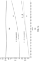
- Figure 10 shows simulated values of generated reference voltage against temperature of the circuit of Figure 8 , compared to a circuit with no compensation, where the top graph shows simulated values of generated reference voltage against temperature of the circuit of Figure 8 , and the lower graph of Figure 10 shows generated reference voltage of a circuit with no compensation.
- This shows the reduced magnitude of ⁇ vref_t due to the compensation, and also the reduced value of ⁇ vref_t as a fraction of Vref itself. This illustrates the improved accuracy and reliability, and reduced variability of Vref as a result of the compensation.
- Figure 11 illustrates schematically an alternative circuit for providing a reference voltage according to an embodiment of the disclosure. Many of the features are the same as those provided in Figure 4 , have similar functionality, and therefore carry the same reference numerals.
- the gate of the second depletion-mode MOSFET 130 is connected to the source of the first enhancement-mode MOSFET 120.
- the source electrode of the first enhancement-mode nMOSFET 120 is connected to a first reference potential 150.
- the first reference potential 150 is a ground potential.
- the substrate electrode of the first enhancement-mode nMOSFET 120 is connected to the source electrode of the first enhancement-mode nMOSFET 120 at a third node. The third node is formed between the source electrode of the first enhancement-mode nMOSFET 120 and the first reference potential 150.
- a second resistor 125 having a resistance Rb is connected in series with the source electrode of the first enhancement-mode nMOSFET 120.
- the second resistor 125 is formed between the first reference potential 150 and the third node.
- the gate of the second depletion-mode MOSFET 130 is connected to the source of the first enhancement-mode MOSFET 120 at an eighth node.
- the eighth node is formed between the third node and the second resistor 125.
- the upper portion of Figure 12 shows the voltage across the second depletion-mode MOSFET 130, Vgs3, and the voltage across the first enhancement-mode nMOSFET 120, Vgs3, against temperature of the circuit 100 of Figure 11 , when M3 is off at lower temperatures and when M3 is on at higher temperatures. If Vgs2 > -Vgs3: then M3 is off, and if Vgs2 ⁇ -Vgs3: then M3 is on, and current I2 generated.
- FIG. 12 shows the compensation provided to the generated reference voltage due to the second depletion-mode MOSFET 130 and the current, I2, through the second depletion-mode MOSFET 130.
- Figure 13 illustrates schematically an alternative circuit for providing a reference voltage according to an embodiment of the disclosure. This is similar to the circuit shown in Figure 11 .
- three first depletion-mode MOSFETS 210a, 210b, 210c are connected in series in place of the one first depletion-mode MOSFET 110 shown in Figure 11
- three first enhancement-mode MOSFETS 220a, 220b, 220c are connected in series in place of the one first enhancement-mode MOSFET 120 shown in Figure 11
- three second depletion-mode MOSFETS 230a, 230b, 230c are connected in parallel in place of the one second depletion-mode MOSFET 130 shown in Figure 11 .
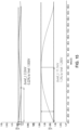
- Figure 14(a) shows simulated values of generated reference voltage against temperature for the circuit of Figure 13 , showing Vref against temperature when compensation is provided.
- Figure 14(b) shows simulated values of current against temperature for the circuit of Figure 13 .
- the upper line shows the combined current, I2, from the second depletion-mode MOSFETS 230a, 230b, 230c.
- the lower line shows the current, I1, through the first depletion-mode MOSFETS 210a, 210b, 210c and the first enhancement-mode MOSFETS 220a, 220b, 220c
- the middle line shows the total current consumption of the circuit, I1 + I2.
- Figure 15 shows simulated values of generated reference voltage against temperature of the circuit of Figure 13 , compared to a circuit with no compensation, where the top graph shows simulated values of generated reference voltage against temperature of the circuit of Figure 13 , and the lower graph of Figure 10 shows generated reference voltage of a circuit with no compensation.
- This shows the reduced magnitude of ⁇ vref_t due to the compensation, and also the reduced value of ⁇ vref_t as a fraction of Vref itself.
- Reference voltage circuit 150 First reference potential 110 First depletion type MOSFET 160 Second reference potential 115 First resistor 170 Reference voltage output 120 Enhancement type MOSFET 180 Additional Circuitry 125 Second resistor 210a-c First depletion type MOSFET 130 Second depletion type MOSFET 220a-c Enhancement type MOSFET 135 Third resistor 230a-c Second depletion type MOSFET 140 Power source
Landscapes
- Engineering & Computer Science (AREA)
- Physics & Mathematics (AREA)
- Electromagnetism (AREA)
- General Physics & Mathematics (AREA)
- Radar, Positioning & Navigation (AREA)
- Automation & Control Theory (AREA)
- Microelectronics & Electronic Packaging (AREA)
- Nonlinear Science (AREA)
- Control Of Electrical Variables (AREA)
Abstract
A reference voltage generating circuit comprising a first depletion type metal-oxide semiconductor field-effect transistor (MOSFET), a first enhancement type MOSFET, a reference voltage output connected between the first depletion type MOSFET and the first enhancement type MOSFET, and a second depletion type MOSFET.
Description
- The present application relates to a reference voltage circuit, particularly but not exclusively, the application relates to a reference voltage circuit having an additional depletion type metal-oxide semiconductor field-effect transistor (MOSFET) configured to provide a current compensation.
- Voltage reference circuits are used to provide a fixed or constant voltage to a device, and are often used to reduce current consumption of a device. Low current consumption circuits are often implemented in the power supply of smaller, less power intensive devices, such as wearable electronics.
- It is known to provide a voltage reference circuit including an enhancement type MOSFET and a depletion type MOSFET to provide a reference voltage, as shown in
Figure 1 . Each MOSFET includes a source, drain and gate electrodes. N-channel (nMOS) and P-channel (pMOS) type MOSFETS also have a fourth terminal known as the substrate. In discrete MOSFETs the substrate is connected to the source terminal. -
Figure 2 shows a graph of the current through the depletion and enhancement MOSFETs, Id, against the voltage between the gate and source of each MOSFET, Vgs1 and Vgs2, in the circuit ofFigure 1 . Vt_DP and Vt_EN represent the voltage through the depletion mode MOSFET and the enhancement mode MOSFET when the current through the device is zero. - The voltage between the gate and source of each MOSFET, Vgs1, Vgs2, and the reference voltage provided follow the below equations when Id=I1, in which L1 and W1 refer to the length and width of the MOS gate:




- The configuration of the circuit can be adjusted such that K2=K1. This is generally done by adjusting W and L, and can only be performed when designing or fabricating the MOSFETs. In general, they cannot be changed using circuit design.

- If the temperature coefficients of Vt_EN and Vt_DP were the same or substantially the same, then

- However, it is generally found that the generated reference voltage, Vref, is dependent upon temperature and ΔVref /ΔT ≠ 0, as demonstrated in
Figure 3 which shows a generated reference voltage, Vref, against the temperature of the circuit ofFigure 1 . The change in generated reference voltage, Vref, due to the temperature is given as Δvref_t. - Δvref_t can be dependent upon the process characteristics of the fabrication process used to manufacture the depletion mode MOSFET and the enhancement mode MOSFET, but is generally found to vary by a few %. For low current consumption power supply, it is desirable to reduce Δvref_t to provide a more reliable and constant reference voltage.
- It is known to introduce additional circuitry to provide a compensation to offset Δvref_t. However, the use of complicated, additional circuitry for this increase the current consumption of the reference voltage generating circuit.
- In general, the present disclosure proposes to overcome at least some of the above problems by providing a reference voltage circuit having an additional depletion type metal-oxide semiconductor field-effect transistor (MOSFET) configured to provide a current compensation.
- For optimal performance of a reference voltage generating circuit, it is desired for Δvref_t to be less than 0.5%-0.75% of Vref. The present disclosure provides a voltage generating circuit that meets this criterion.
- Aspects and preferred features are set out in the accompanying claims.
- According to a first aspect of the disclosure, there is provided a reference voltage generating circuit comprising:
- a first depletion type metal-oxide semiconductor field-effect transistor (MOSFET) having a source electrode, a drain electrode, and a gate electrode, and
wherein the drain electrode of the first depletion type MOSFET is configured to be connected to a supply potential, and the gate electrode of the first depletion type MOSFET is connected to the source of the first depletion type MOSFET; - a first enhancement type MOSFET having a source electrode, a drain electrode, and a gate electrode, and
wherein the drain electrode of the first enhancement type MOSFET is connected to the source electrode of the first depletion type MOSFET, the gate electrode of the first enhancement type MOSFET is connected to the drain of the first enhancement type MOSFET, and the source electrode of the first enhancement type MOSFET is connected to a first reference potential; - a reference voltage output connected between the source electrode of the first depletion type MOSFET and the drain electrode of the first enhancement type MOSFET; and
- a second depletion type MOSFET having a source electrode, a drain electrode, and a gate electrode, and
wherein the drain electrode of the second depletion type MOSFET is connected between the supply potential and the drain electrode of the first depletion type MOSFET, and the source electrode of the second depletion type MOSFET is connected between the source electrode of the first depletion type MOSFET and the drain electrode of the first enhancement type MOSFET. - Each of the first depletion type MOSFET and the first enhancement type MOSFET may comprise a substrate electrode.
- Each of the first depletion type MOSFET and the first enhancement type MOSFET may comprise N-channel MOSFETs. Alternatively, each of the first depletion type MOSFET and the first enhancement type MOSFET may comprise P-channel MOSFETs
- The reference voltage generating circuit may further comprise a first resistor connected between the source of the first depletion type MOSFET and the substrate of the first depletion type MOSFET, and a second resistor connected between the source of the first enhancement type MOSFET and the substrate of the first enhancement type MOSFET.
- A ratio of a resistance of the first resistor and a resistance of the second resistor is configured such that a voltage of the reference voltage output decreases with increasing temperature.
- The resistance of the first resistor may be less than the resistance of the second resistor
- The second depletion type MOSFET may comprise a substrate electrode.
- The second depletion type MOSFET may comprise an N-channel MOSFET. Alternatively, the second depletion type MOSFET may comprise a P-channel MOSFET.
- The reference voltage generating circuit may further comprise a third resistor connected between the source of the first depletion type MOSFET and the substrate of the second depletion type MOSFET.
- The gate electrode of the second depletion type MOSFET may be connected to a second reference potential.
- The first reference potential and the second reference potential may be the same reference potential.
- The first reference potential and/or the second reference potential may be ground potential.
- The gate of the second depletion type MOSFET may be connected to the source of the first enhancement type MOSFET.
- The source of the second depletion type MOSFET may be connected between the drain of the first enhancement type MOSFET and the reference voltage output.
- The reference voltage generating circuit may further comprise
- one or more additional first depletion type MOSFETs connected in series with the first depletion type MOSFET; and/or
- one or more additional first enhancement type MOSFETs connected in series with the first enhancement type MOSFET;
- one or more additional second depletion type MOSFETs connected in parallel with the second depletion type MOSFET.
- According to a further aspect of the disclosure, there is provided a method of manufacturing a reference voltage generating circuit, the method comprising:
- forming a first depletion type metal-oxide semiconductor field-effect transistor (MOSFET) having a source electrode, a drain electrode, and a gate electrode, and
wherein the drain electrode of the first depletion type MOSFET is configured to be connected to a supply potential, and the gate electrode of the first depletion type MOSFET is connected to the source of the first depletion type MOSFET; - forming a first enhancement type MOSFET having a source electrode, a drain electrode, and a gate electrode, and
wherein the drain electrode of the first enhancement type MOSFET is connected to the source electrode of the first depletion type MOSFET, the gate electrode of the first enhancement type MOSFET is connected to the drain of the first enhancement type MOSFET, and the source electrode of the first enhancement type MOSFET is connected to a first reference potential; - forming a reference voltage output connected between the source electrode of the first depletion type MOSFET and the drain electrode of the first enhancement type MOSFET; and
- a second depletion type MOSFET having a source electrode, a drain electrode, and a gate electrode, and
wherein the drain electrode of the second depletion type MOSFET is connected between the supply potential and the drain electrode of the first depletion type MOSFET, and the source electrode of the second depletion type MOSFET is connected between the source electrode of the first depletion type MOSFET and the drain electrode of the first enhancement type MOSFET. - The proposed device provides the following advantages:
- The reference voltage generating circuit provides a reference voltage that has a reduced temperature coefficient compared to state-of-the-art reference voltage generating circuits;
- The reference voltage generating circuit is simplifier than state-of-the-art devices, with only an additional depletion mode MOSFET and a resistor, whilst still providing a reduced Δvref_t;
- The current consumption of the additional components of the circuit is reduced compared to alternative reference voltage generating circuits;
- There is only a small increase of current consumption due to the additional components because the compensation provided is effective at high temperature;
- The compensation of the reference voltage generating circuit may be realized by a direct power source and an additional current with a positive temperature coefficient to reference voltage.
- Some embodiments of the disclosure will now be described, by way of example only and with reference to the accompanying drawings, in which:
-
Figure 1 illustrates schematically an example circuit for providing a reference voltage according to the state-of-the-art; -
Figure 2 shows a graph of the current against the voltage for a pair of depletion and enhancement MOSFETs in an example circuit for providing a reference voltage according to the state-of-the-art; -
Figure 3 shows a graph of the generated reference voltage against temperature of an example circuit for providing a reference voltage according to the state-of-the-art; -
Figure 4 illustrates schematically a circuit for providing a reference voltage according to an embodiment of the disclosure; -
Figure 5 shows graphs of current provided by an additional depletion type MOSFET, the voltage across the additional depletion type MOSFET, and a generated reference voltage against temperature of the circuit ofFigure 4 ; -
Figure 6 shows a graph of the current against the voltage of an additional depletion type MOSFET of a circuit for providing a reference voltage according to an embodiment of the disclosure; -
Figure 7 shows a graph of the generated reference voltage against temperature of a circuit for providing a reference voltage according to an embodiment of the disclosure; -
Figure 8 illustrates schematically an alternative circuit for providing a reference voltage according to an embodiment of the disclosure; -
Figure 9 shows both a graph of simulated values of generated reference voltage against temperature and of current against temperature in the circuit ofFigure 8 ; -
Figure 10 shows a graph of simulated values of generated reference voltage against temperature of the circuit ofFigure 8 ; -
Figure 11 illustrates schematically an alternative circuit for providing a reference voltage according to an embodiment of the disclosure; -
Figure 12 shows graphs of current provided by an additional depletion type MOSFET, the voltage across the additional depletion type MOSFET, and a generated reference voltage against temperature of the circuit ofFigure 11 ; -
Figure 13 illustrates schematically an alternative circuit for providing a reference voltage according to an embodiment of the disclosure; -
Figure 14 shows both a graph of simulated values of generated reference voltage against temperature and of current against temperature in the circuit ofFigure 13 ; and -
Figure 15 shows a graph of simulated values of generated reference voltage against temperature of the circuit ofFigure 13 . -
Figure 4 illustrates acircuit 100 or module for providing a reference voltage according to an embodiment of the disclosure. Thecircuit 100 includes a first depletion-mode (also referred to as a normally-on), n-type metal-oxide semiconductor field-effect transistor (nMOSFET) 110. The first depletion-mode nMOSFET 110 has a source electrode, a drain electrode, a gate electrode, and a substrate electrode. The gate of the first depletion-mode nMOSFET 110 is connected to the source of the first depletion-mode nMOSFET 110 at a first node. A voltage measured between the gate and the source of the first depletion-mode nMOSFET 110 is given as Vgs1. The drain electrode of the first depletion-mode nMOSFET 110 is connected to apower source 140. In this example, the power source is a voltage cell or battery. Thepower source 140 provides a voltage VDD. - The substrate electrode of the first depletion-
mode nMOSFET 110 is also connected to the source of the first depletion-mode nMOSFET 110. In this example, the substrate electrode of the first depletion-mode nMOSFET 110 is also connected to the source of the first depletion-mode nMOSFET 110 at the first node. Alternatively, the substrate electrode of the first depletion-mode nMOSFET 110 may be connected to a reference potential, such as ground potential. Afirst resistor 115 having a resistance Ra is connected to the source electrode of the first depletion-mode nMOSFET 110. Thefirst resistor 115 is formed between the source electrode of the first depletion-mode nMOSFET 110 and the first node where both the gate and the substrate electrode of the first depletion-mode nMOSFET 110 are connected to the source electrode of the first depletion-mode nMOSFET 110. - A first enhancement-mode (also referred to as a normally-off)
nMOSFET 120 is connected in series with the first depletion-mode nMOSFET 110. The first enhancement-mode nMOSFET 120 has a source electrode, a drain electrode, a gate electrode, and a substrate electrode. The drain electrode of the first enhancement-mode nMOSFET 120 is connected to the source electrode of the first depletion-mode nMOSFET 110. The gate electrode of the first enhancement-mode nMOSFET 120 is connected to the drain electrode of the first enhancement-mode nMOSFET 120 at a second node. Both the first and second nodes are formed between the first depletion-mode nMOSFET 110 and the first enhancement-mode nMOSFET 120. - The source electrode of the first enhancement-
mode nMOSFET 120 is connected to afirst reference potential 150. In this example, thefirst reference potential 150 is a ground potential. A voltage between the gate and the source of the first enhancement-mode nMOSFET 120 is given as Vgs2. The substrate electrode of the first enhancement-mode nMOSFET 120 is connected to the source electrode of the first enhancement-mode nMOSFET 120 at a third node. The third node is formed between the source electrode of the first enhancement-mode nMOSFET 120 and thefirst reference potential 150. - A
second resistor 125 having a resistance Rb is connected to the source electrode of the first enhancement-mode nMOSFET 120. Thesecond resistor 125 is formed between the source electrode of the first enhancement-mode nMOSFET 120 and the third node. As shown inFigure 2 , for a reference voltage generating circuit having a depletion mode MOSFET and an enhancement mode MOSFET connected in series, the voltage, Vgs1, between the gate and the source of the first depletion-mode nMOSFET 110 and the voltage, Vgs2, between the gate and the source of the first enhancement-mode nMOSFET 120 are similarly dependent on the current through them, I1. Consequently, the inclusion of the first and second resistors reduces the current, I1, whilst maintaining the reference voltage generated, Vref. - An
output 170 for the generated reference voltage Vref is connected between the first depletion-mode nMOSFET 110 and the first enhancement-mode nMOSFET 120. In this example, theoutput 170 is connected to a fourth node located between the first node and the second node. - The
circuit 100 includesadditional circuitry 180, theadditional circuitry 180 including a second depletion-mode nMOSFET 130 connected in parallel with the first depletion-mode nMOSFET 110. The second depletion-mode nMOSFET 130 has a source electrode, a drain electrode, a gate electrode, and a substrate electrode. The drain electrode of the second depletion-mode nMOSFET 130 is connected to the drain electrode of the first depletion-mode nMOSFET 110 and is connected to thepower source 140. The drain electrode of the second depletion-mode nMOSFET 130 is connected to a fifth node located between the drain electrode of the first depletion-mode nMOSFET 110 and thepower source 140. - The gate of the second depletion-
mode nMOSFET 130 is connected to asecond reference potential 160. In this example, thesecond reference potential 160 is a ground potential. - The source electrode of the second depletion-
mode nMOSFET 130 is connected to the source electrode of the first depletion-mode nMOSFET 110 and to the drain electrode of the first enhancement-mode nMOSFET 120. The source electrode of the second depletion-mode nMOSFET 130 is connected to a sixth node located between the second node and the fourth node. A voltage measured between the gate and the source of the second depletion-mode nMOSFET 110 is given as Vgs3. - The substrate electrode of the second depletion-
mode nMOSFET 130 is connected to the source electrode of the second depletion-mode nMOSFET 130 at a seventh node. The seventh node is formed between the source electrode of the second depletion-mode nMOSFET 130 and the sixth node. Athird resistor 135 having a resistance Rc is connected to the source electrode of the second depletion-mode nMOSFET 130. Thethird resistor 135 is formed between the source electrode of the second depletion-mode nMOSFET 130 and the seventh node. - The current through the first depletion-
mode nMOSFET 110 and the first enhancement-mode nMOSFET 120 is given as I1. The current through the second depletion-mode nMOSFET 130 is given as I2. - The upper portion of
Figure 5 shows the voltage across the second depletion-mode MOSFET 130, Vgs3, and the generated reference voltage, Vref, against temperature of thecircuit 100 ofFigure 4 , when the second depletion-mode MOSFET 130, herein referred to as M3, is off at lower temperatures and when M3 is on at higher temperatures. If Vref > -Vgs3: then M3 is off, and if Vref < -Vgs3: then M3 is on, and the current I2 is generated. The dashed line illustrates the the voltage of -Vgs3 in a situation where there is no Vref connection to the circuit. Vgs3 is the voltage measured between the gate and the source of the second depletion-mode nMOSFET 110. As the source node has a higher voltage than that of the gate node, Vgs3 is a negative value. - The lower portion of
Figure 5 shows the compensation provided to the generated reference voltage due to the second depletion-mode MOSFET 130 and the current, I2, through the second depletion-mode MOSFET 130. If Vref > -Vgs3: then M3 is off current is not generated by the resistor, and if Vref < -Vgs3: then M3 is on, and the current I2 is generated by the resistor.Figure 6 shows a graph of the current, I2, against the voltage, Vgs3, of the second depletion-mode MOSFET 130 of the circuit ofFigure 4 for three different temperatures. -
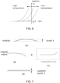
Figure 7 shows the generated reference voltage against temperature, including the compensation provided by a second depletion-mode MOSFET as shown inFigure 4 . -
Figure 7(a) shows the generated reference voltage against temperature for a reference voltage generating circuit without a second depletion-mode MOSFET 130 to introduce compensation. The change in generated reference voltage, Vref, due to the temperature is given as Δvref_t; -
Figure 7(b) shows an adjusted generated reference voltage against temperature, similar to the reference voltage shown inFigure 7(a) . The magnitude of Δvref_t is not changed by this adjustment, however the change in reference voltage due to temperature, Δvref_t, does occur less at lower temperatures and more at higher temperatures. This adjustment is provided by selecting values of Ra and Rb, and K1 and K2 to provide the adjustment. In general, if Rb/Ra < 1, then Δvref_t will be adjusted as shown inFigure 7(b) ; -
Figure 7(c) shows the compensation provided to the reference voltage by I2 and the second depletion-mode MOSFET 130. The compensation increases Vref at higher temperatures; and -
Figure 7(d) shows the resulting Vref from adding the adjusted Vref ofFigure 7(b) to the compensating voltage ofFigure 7(c) . As the adjusted Vref ofFigure 7(b) has a decreasing Vref at higher temperatures, and the compensating voltage ofFigure 7(c) has an increasing voltage at higher temperatures, the magnitude of the resulting Δvref_t shown inFigure 7(d) is significantly reduced. -
Figure 8 illustrates schematically an alternative circuit for providing a reference voltage according to an embodiment of the disclosure. This is similar to the circuit shown inFigure 4 , and therefore has similar reference numerals. However, in this embodiment, three first depletion-mode MOSFETS mode MOSFET 110 shown inFigure 4 , three first enhancement-mode MOSFETS mode MOSFET 120 shown inFigure 4 , and three second depletion-mode MOSFETS mode MOSFET 130 shown inFigure 4 . Although the first depletion-mode MOSFETS mode MOSFETS mode MOSFETS -
Figure 9(a) shows simulated values of generated reference voltage against temperature for the circuit ofFigure 8 . The top line shows Vref against temperature when compensation is provided, and the lower line shows Vref against temperature when compensation is not provided. -
Figure 9(b) shows simulated values of current against temperature for the circuit ofFigure 8 . The lower line shows the combined current, I2, from the second depletion-mode MOSFETS mode MOSFETS mode MOSFETS -
Figure 10 shows simulated values of generated reference voltage against temperature of the circuit ofFigure 8 , compared to a circuit with no compensation, where the top graph shows simulated values of generated reference voltage against temperature of the circuit ofFigure 8 , and the lower graph ofFigure 10 shows generated reference voltage of a circuit with no compensation. This shows the reduced magnitude of Δvref_t due to the compensation, and also the reduced value of Δvref_t as a fraction of Vref itself. This illustrates the improved accuracy and reliability, and reduced variability of Vref as a result of the compensation. -
Figure 11 illustrates schematically an alternative circuit for providing a reference voltage according to an embodiment of the disclosure. Many of the features are the same as those provided inFigure 4 , have similar functionality, and therefore carry the same reference numerals. In this embodiment, the gate of the second depletion-mode MOSFET 130 is connected to the source of the first enhancement-mode MOSFET 120. - The source electrode of the first enhancement-
mode nMOSFET 120 is connected to afirst reference potential 150. In this example, thefirst reference potential 150 is a ground potential. The substrate electrode of the first enhancement-mode nMOSFET 120 is connected to the source electrode of the first enhancement-mode nMOSFET 120 at a third node. The third node is formed between the source electrode of the first enhancement-mode nMOSFET 120 and thefirst reference potential 150. - A
second resistor 125 having a resistance Rb is connected in series with the source electrode of the first enhancement-mode nMOSFET 120. Thesecond resistor 125 is formed between thefirst reference potential 150 and the third node. The gate of the second depletion-mode MOSFET 130 is connected to the source of the first enhancement-mode MOSFET 120 at an eighth node. The eighth node is formed between the third node and thesecond resistor 125. - The upper portion of
Figure 12 shows the voltage across the second depletion-mode MOSFET 130, Vgs3, and the voltage across the first enhancement-mode nMOSFET 120, Vgs3, against temperature of thecircuit 100 ofFigure 11 , when M3 is off at lower temperatures and when M3 is on at higher temperatures. If Vgs2 > -Vgs3: then M3 is off, and if Vgs2 < -Vgs3: then M3 is on, and current I2 generated. - The lower portion of
Figure 12 shows the compensation provided to the generated reference voltage due to the second depletion-mode MOSFET 130 and the current, I2, through the second depletion-mode MOSFET 130. -
Figure 13 illustrates schematically an alternative circuit for providing a reference voltage according to an embodiment of the disclosure. This is similar to the circuit shown inFigure 11 . However, in this embodiment, three first depletion-mode MOSFETS mode MOSFET 110 shown inFigure 11 , three first enhancement-mode MOSFETS mode MOSFET 120 shown inFigure 11 , and three second depletion-mode MOSFETS mode MOSFET 130 shown inFigure 11 . -
Figure 14(a) shows simulated values of generated reference voltage against temperature for the circuit ofFigure 13 , showing Vref against temperature when compensation is provided. -
Figure 14(b) shows simulated values of current against temperature for the circuit ofFigure 13 . The upper line shows the combined current, I2, from the second depletion-mode MOSFETS mode MOSFETS mode MOSFETS -
Figure 15 shows simulated values of generated reference voltage against temperature of the circuit ofFigure 13 , compared to a circuit with no compensation, where the top graph shows simulated values of generated reference voltage against temperature of the circuit ofFigure 13 , and the lower graph ofFigure 10 shows generated reference voltage of a circuit with no compensation. This shows the reduced magnitude of Δvref_t due to the compensation, and also the reduced value of Δvref_t as a fraction of Vref itself. - Although specific embodiments have been described above, the claims are not limited to those embodiments. Each feature disclosed herein may be incorporated in any of the described embodiments, alone or in an appropriate combination with other features disclosed herein.
-
100 Reference voltage circuit 150 First reference potential 110 First depletion type MOSFET 160 Second reference potential 115 First resistor 170 Reference voltage output 120 Enhancement type MOSFET 180 Additional Circuitry 125 Second resistor 210a-c First depletion type MOSFET 130 Second depletion type MOSFET 220a-c Enhancement type MOSFET 135 Third resistor 230a-c Second depletion type MOSFET 140 Power source
Claims (16)
- A reference voltage generating circuit comprising:a first depletion type metal-oxide semiconductor field-effect transistor (MOSFET) having a source electrode, a drain electrode, and a gate electrode, and
wherein the drain electrode of the first depletion type MOSFET is configured to be connected to a supply potential, and the gate electrode of the first depletion type MOSFET is connected to the source of the first depletion type MOSFET;a first enhancement type MOSFET having a source electrode, a drain electrode, and a gate electrode, and
wherein the drain electrode of the first enhancement type MOSFET is connected to the source electrode of the first depletion type MOSFET, the gate electrode of the first enhancement type MOSFET is connected to the drain of the first enhancement type MOSFET, and the source electrode of the first enhancement type MOSFET is connected to a first reference potential;a reference voltage output connected between the source electrode of the first depletion type MOSFET and the drain electrode of the first enhancement type MOSFET; anda second depletion type MOSFET having a source electrode, a drain electrode, and a gate electrode, and
wherein the drain electrode of the second depletion type MOSFET is connected between the supply potential and the drain electrode of the first depletion type MOSFET, and the source electrode of the second depletion type MOSFET is connected between the source electrode of the first depletion type MOSFET and the drain electrode of the first enhancement type MOSFET. - A reference voltage generating circuit according to claim 1, wherein each of the first depletion type MOSFET and the first enhancement type MOSFET comprise a substrate electrode.
- A reference voltage generating circuit according to claim 2, wherein each of the first depletion type MOSFET and the first enhancement type MOSFET comprise N-channel MOSFETs.
- A reference voltage generating circuit according to claim 2 or 3, further comprising:a first resistor connected between the source of the first depletion type MOSFET and the substrate of the first depletion type MOSFET; anda second resistor connected between the source of the first enhancement type MOSFET and the substrate of the first enhancement type MOSFET.
- A reference voltage generating circuit according to claim 4, wherein a ratio of a resistance of the first resistor and a resistance of the second resistor is configured such that a voltage of the reference voltage output decreases with increasing temperature.
- A reference voltage generating circuit according to claim 5, wherein the resistance of the first resistor is less than the resistance of the second resistor.
- A reference voltage generating circuit according to any preceding claim, wherein the second depletion type MOSFET comprises a substrate electrode.
- A reference voltage generating circuit according to claim 7, wherein the second depletion type MOSFET comprises an N-channel MOSFET.
- A reference voltage generating circuit according to claim 7 or 8, further comprising a third resistor connected between the source of the first depletion type MOSFET and the substrate of the second depletion type MOSFET.
- A reference voltage generating circuit according to any preceding claim, wherein the gate electrode of the second depletion type MOSFET is connected to a second reference potential.
- A reference voltage generating circuit according to claim 10, wherein the first reference potential and the second reference potential are the same reference potential.
- A reference voltage generating circuit according to any preceding claim, wherein the first reference potential and/or the second reference potential are ground potential.
- A reference voltage generating circuit according to any of claims 1 to 9, wherein the gate of the second depletion type MOSFET is connected to the source of the first enhancement type MOSFET.
- A reference voltage generating circuit according to any preceding claim, wherein the source of the second depletion type MOSFET is connected between the drain of the first enhancement type MOSFET and the reference voltage output.
- A reference voltage generating circuit according to any preceding claim, further comprising:one or more additional first depletion type MOSFETs connected in series with the first depletion type MOSFET;one or more additional first enhancement type MOSFETs connected in series with the first enhancement type MOSFET;one or more additional second depletion type MOSFETs connected in series with the second depletion type MOSFET.
- A method of manufacturing a reference voltage generating circuit, the method comprising:forming a first depletion type metal-oxide semiconductor field-effect transistor (MOSFET) having a source electrode, a drain electrode, and a gate electrode, and
wherein the drain electrode of the first depletion type MOSFET is configured to be connected to a supply potential, and the gate electrode of the first depletion type MOSFET is connected to the source of the first depletion type MOSFET;forming a first enhancement type MOSFET having a source electrode, a drain electrode, and a gate electrode, and
wherein the drain electrode of the first enhancement type MOSFET is connected to the source electrode of the first depletion type MOSFET, the gate electrode of the first enhancement type MOSFET is connected to the drain of the first enhancement type MOSFET, and the source electrode of the first enhancement type MOSFET is connected to a first reference potential;forming a reference voltage output connected between the source electrode of the first depletion type MOSFET and the drain electrode of the first enhancement type MOSFET; anda second depletion type MOSFET having a source electrode, a drain electrode, and a gate electrode, and
wherein the drain electrode of the second depletion type MOSFET is connected between the supply potential and the drain electrode of the first depletion type MOSFET, and the source electrode of the second depletion type MOSFET is connected between the source electrode of the first depletion type MOSFET and the drain electrode of the first enhancement type MOSFET.
Priority Applications (6)
| Application Number | Priority Date | Filing Date | Title |
|---|---|---|---|
| EP23164072.3A EP4435554A1 (en) | 2023-03-24 | 2023-03-24 | Reference voltage circuit |
| CN202311250316.1A CN117130423B (en) | 2023-03-24 | 2023-09-26 | Reference voltage circuit |
| CN202410326594.9A CN118732765A (en) | 2023-03-24 | 2024-03-21 | Reference voltage circuit |
| US18/614,096 US20240321878A1 (en) | 2023-03-24 | 2024-03-22 | Reference Voltage Circuit |
| US18/614,055 US20240321877A1 (en) | 2023-03-24 | 2024-03-22 | Reference Voltage Circuit |
| EP24165417.7A EP4435555A1 (en) | 2023-03-24 | 2024-03-22 | Reference voltage circuit |
Applications Claiming Priority (1)
| Application Number | Priority Date | Filing Date | Title |
|---|---|---|---|
| EP23164072.3A EP4435554A1 (en) | 2023-03-24 | 2023-03-24 | Reference voltage circuit |
Publications (1)
| Publication Number | Publication Date |
|---|---|
| EP4435554A1 true EP4435554A1 (en) | 2024-09-25 |
Family
ID=85726121
Family Applications (2)
| Application Number | Title | Priority Date | Filing Date |
|---|---|---|---|
| EP23164072.3A Pending EP4435554A1 (en) | 2023-03-24 | 2023-03-24 | Reference voltage circuit |
| EP24165417.7A Pending EP4435555A1 (en) | 2023-03-24 | 2024-03-22 | Reference voltage circuit |
Family Applications After (1)
| Application Number | Title | Priority Date | Filing Date |
|---|---|---|---|
| EP24165417.7A Pending EP4435555A1 (en) | 2023-03-24 | 2024-03-22 | Reference voltage circuit |
Country Status (3)
| Country | Link |
|---|---|
| US (2) | US20240321877A1 (en) |
| EP (2) | EP4435554A1 (en) |
| CN (2) | CN117130423B (en) |
Families Citing this family (1)
| Publication number | Priority date | Publication date | Assignee | Title |
|---|---|---|---|---|
| IT202300006477A1 (en) * | 2023-04-03 | 2024-10-03 | VOLTAGE REGULATION CIRCUIT |
Citations (5)
| Publication number | Priority date | Publication date | Assignee | Title |
|---|---|---|---|---|
| US4417263A (en) * | 1980-02-01 | 1983-11-22 | Kabushiki Kaisha Daini Seikosha | Semiconductor device |
| US9632521B2 (en) * | 2013-03-13 | 2017-04-25 | Analog Devices Global | Voltage generator, a method of generating a voltage and a power-up reset circuit |
| US20200257325A1 (en) * | 2019-02-08 | 2020-08-13 | Ablic Inc. | Reference voltage circuit and semiconductor device |
| US11275399B2 (en) * | 2017-06-01 | 2022-03-15 | Ablic Inc. | Reference voltage circuit including depletion type and enhancement type transistors in a common centroid arrangement |
| US20220209769A1 (en) * | 2020-12-28 | 2022-06-30 | LAPIS Technology Co., Ltd. | Semiconductor device |
Family Cites Families (11)
| Publication number | Priority date | Publication date | Assignee | Title |
|---|---|---|---|---|
| US4978904A (en) * | 1987-12-15 | 1990-12-18 | Gazelle Microcircuits, Inc. | Circuit for generating reference voltage and reference current |
| US4937477A (en) * | 1988-01-19 | 1990-06-26 | Supertex, Inc. | Integrated mos high-voltage level-translation circuit, structure and method |
| CN101632176A (en) * | 2007-01-24 | 2010-01-20 | 克伊斯通半导体有限公司 | Depletion mode MOSFET circuit and application |
| JP5051105B2 (en) * | 2008-11-21 | 2012-10-17 | 三菱電機株式会社 | Reference voltage generation circuit and bias circuit |
| CN102880215B (en) * | 2012-09-17 | 2014-07-09 | 电子科技大学 | Voltage reference source with low power consumption and low temperature coefficient |
| JP7000187B2 (en) * | 2018-02-08 | 2022-01-19 | エイブリック株式会社 | Reference voltage circuit and semiconductor device |
| US10725491B2 (en) * | 2018-12-05 | 2020-07-28 | Texas Instruments Incorporated | Methods and apparatus to correct gate bias for a diode-connected transistor |
| JP7175172B2 (en) * | 2018-12-12 | 2022-11-18 | エイブリック株式会社 | Reference voltage generator |
| CN111146770B (en) * | 2019-12-31 | 2021-06-01 | 三维通信股份有限公司 | Protection circuit of GaN power device |
| US20230135542A1 (en) * | 2020-02-25 | 2023-05-04 | Rohm Co., Ltd. | Constant voltage generation circuit |
| US11474552B2 (en) * | 2021-03-04 | 2022-10-18 | Taiwan Semiconductor Manufacturing Company, Ltd. | Voltage reference temperature compensation circuits and methods |
-
2023
- 2023-03-24 EP EP23164072.3A patent/EP4435554A1/en active Pending
- 2023-09-26 CN CN202311250316.1A patent/CN117130423B/en active Active
-
2024
- 2024-03-21 CN CN202410326594.9A patent/CN118732765A/en active Pending
- 2024-03-22 EP EP24165417.7A patent/EP4435555A1/en active Pending
- 2024-03-22 US US18/614,055 patent/US20240321877A1/en active Pending
- 2024-03-22 US US18/614,096 patent/US20240321878A1/en active Pending
Patent Citations (5)
| Publication number | Priority date | Publication date | Assignee | Title |
|---|---|---|---|---|
| US4417263A (en) * | 1980-02-01 | 1983-11-22 | Kabushiki Kaisha Daini Seikosha | Semiconductor device |
| US9632521B2 (en) * | 2013-03-13 | 2017-04-25 | Analog Devices Global | Voltage generator, a method of generating a voltage and a power-up reset circuit |
| US11275399B2 (en) * | 2017-06-01 | 2022-03-15 | Ablic Inc. | Reference voltage circuit including depletion type and enhancement type transistors in a common centroid arrangement |
| US20200257325A1 (en) * | 2019-02-08 | 2020-08-13 | Ablic Inc. | Reference voltage circuit and semiconductor device |
| US20220209769A1 (en) * | 2020-12-28 | 2022-06-30 | LAPIS Technology Co., Ltd. | Semiconductor device |
Also Published As
| Publication number | Publication date |
|---|---|
| CN118732765A (en) | 2024-10-01 |
| US20240321877A1 (en) | 2024-09-26 |
| CN117130423B (en) | 2025-08-19 |
| US20240321878A1 (en) | 2024-09-26 |
| CN117130423A (en) | 2023-11-28 |
| EP4435555A1 (en) | 2024-09-25 |
Similar Documents
| Publication | Publication Date | Title |
|---|---|---|
| US4417263A (en) | Semiconductor device | |
| EP0058958A2 (en) | Complementary MOSFET logic circuit | |
| JPH08335122A (en) | Semiconductor device for reference voltage | |
| US5514948A (en) | Reference voltage generating circuit | |
| US20090302931A1 (en) | Low-power voltage reference | |
| US5565375A (en) | Method of fabricating a self-cascoding CMOS device | |
| US10860046B2 (en) | Reference voltage generation device | |
| US6628161B2 (en) | Reference voltage circuit | |
| TW419894B (en) | VT reference voltage for extremely low power supply | |
| JP4117780B2 (en) | Reference voltage circuit and electronic equipment | |
| WO2002050911A1 (en) | Ultra-low power basic blocks and their uses | |
| US6184745B1 (en) | Reference voltage generating circuit | |
| EP4435555A1 (en) | Reference voltage circuit | |
| JP2674669B2 (en) | Semiconductor integrated circuit | |
| US4978631A (en) | Current source with a process selectable temperature coefficient | |
| JPS6153860B2 (en) | ||
| US6696895B2 (en) | Push-pull amplifier | |
| EP0948762A1 (en) | Voltage regulator circuits and semiconductor circuit devices | |
| US20100289563A1 (en) | Method and Mechanism to Reduce Current Variation in a Current Reference Branch Circuit | |
| US5272369A (en) | Circuit element with elimination of kink effect | |
| US4940910A (en) | Temperature compensated monolithic delay circuit | |
| US9805990B2 (en) | FDSOI voltage reference | |
| JPH09325826A (en) | Temperature compensation type reference voltage generation circuit | |
| US6441650B2 (en) | Offset comparator and method for forming same | |
| US6492680B1 (en) | Semiconductor integrated circuit device |
Legal Events
| Date | Code | Title | Description |
|---|---|---|---|
| PUAI | Public reference made under article 153(3) epc to a published international application that has entered the european phase |
Free format text: ORIGINAL CODE: 0009012 |
|
| STAA | Information on the status of an ep patent application or granted ep patent |
Free format text: STATUS: THE APPLICATION HAS BEEN PUBLISHED |
|
| AK | Designated contracting states |
Kind code of ref document: A1 Designated state(s): AL AT BE BG CH CY CZ DE DK EE ES FI FR GB GR HR HU IE IS IT LI LT LU LV MC ME MK MT NL NO PL PT RO RS SE SI SK SM TR |
|
| STAA | Information on the status of an ep patent application or granted ep patent |
Free format text: STATUS: REQUEST FOR EXAMINATION WAS MADE |
|
| 17P | Request for examination filed |
Effective date: 20250324 |