EP4435495A1 - Optical structure and display device - Google Patents
Optical structure and display device Download PDFInfo
- Publication number
- EP4435495A1 EP4435495A1 EP24164220.6A EP24164220A EP4435495A1 EP 4435495 A1 EP4435495 A1 EP 4435495A1 EP 24164220 A EP24164220 A EP 24164220A EP 4435495 A1 EP4435495 A1 EP 4435495A1
- Authority
- EP
- European Patent Office
- Prior art keywords
- light
- transmitting layer
- retardation film
- phase
- phase retardation
- Prior art date
- Legal status (The legal status is an assumption and is not a legal conclusion. Google has not performed a legal analysis and makes no representation as to the accuracy of the status listed.)
- Granted
Links
Images


Classifications
-
- G—PHYSICS
- G02—OPTICS
- G02B—OPTICAL ELEMENTS, SYSTEMS OR APPARATUS
- G02B5/00—Optical elements other than lenses
- G02B5/30—Polarising elements
- G02B5/3083—Birefringent or phase retarding elements
-
- G—PHYSICS
- G02—OPTICS
- G02B—OPTICAL ELEMENTS, SYSTEMS OR APPARATUS
- G02B27/00—Optical systems or apparatus not provided for by any of the groups G02B1/00 - G02B26/00, G02B30/00
- G02B27/01—Head-up displays
- G02B27/0101—Head-up displays characterised by optical features
-
- G—PHYSICS
- G02—OPTICS
- G02B—OPTICAL ELEMENTS, SYSTEMS OR APPARATUS
- G02B1/00—Optical elements characterised by the material of which they are made; Optical coatings for optical elements
- G02B1/08—Optical elements characterised by the material of which they are made; Optical coatings for optical elements made of polarising materials
-
- G—PHYSICS
- G02—OPTICS
- G02B—OPTICAL ELEMENTS, SYSTEMS OR APPARATUS
- G02B27/00—Optical systems or apparatus not provided for by any of the groups G02B1/00 - G02B26/00, G02B30/00
- G02B27/01—Head-up displays
- G02B27/017—Head mounted
- G02B27/0172—Head mounted characterised by optical features
-
- G—PHYSICS
- G02—OPTICS
- G02B—OPTICAL ELEMENTS, SYSTEMS OR APPARATUS
- G02B5/00—Optical elements other than lenses
- G02B5/20—Filters
- G02B5/26—Reflecting filters
-
- G—PHYSICS
- G02—OPTICS
- G02B—OPTICAL ELEMENTS, SYSTEMS OR APPARATUS
- G02B27/00—Optical systems or apparatus not provided for by any of the groups G02B1/00 - G02B26/00, G02B30/00
- G02B27/01—Head-up displays
- G02B27/0101—Head-up displays characterised by optical features
- G02B2027/0118—Head-up displays characterised by optical features comprising devices for improving the contrast of the display / brillance control visibility
-
- G—PHYSICS
- G02—OPTICS
- G02B—OPTICAL ELEMENTS, SYSTEMS OR APPARATUS
- G02B27/00—Optical systems or apparatus not provided for by any of the groups G02B1/00 - G02B26/00, G02B30/00
- G02B27/01—Head-up displays
- G02B27/0101—Head-up displays characterised by optical features
- G02B2027/0123—Head-up displays characterised by optical features comprising devices increasing the field of view
-
- G—PHYSICS
- G02—OPTICS
- G02B—OPTICAL ELEMENTS, SYSTEMS OR APPARATUS
- G02B27/00—Optical systems or apparatus not provided for by any of the groups G02B1/00 - G02B26/00, G02B30/00
- G02B27/01—Head-up displays
- G02B27/017—Head mounted
- G02B2027/0178—Eyeglass type
-
- G—PHYSICS
- G02—OPTICS
- G02B—OPTICAL ELEMENTS, SYSTEMS OR APPARATUS
- G02B27/00—Optical systems or apparatus not provided for by any of the groups G02B1/00 - G02B26/00, G02B30/00
- G02B27/28—Optical systems or apparatus not provided for by any of the groups G02B1/00 - G02B26/00, G02B30/00 for polarising
- G02B27/286—Optical systems or apparatus not provided for by any of the groups G02B1/00 - G02B26/00, G02B30/00 for polarising for controlling or changing the state of polarisation, e.g. transforming one polarisation state into another
Definitions
- the present disclosure relates to an optical structure and a display device.
- Virtual Reality (VR) device in combination with computer and sensor technology, enables users to experience the sense of immersion in an interactive three-dimensional environment.
- virtual reality devices include glasses, which adopt an ultra-short focus folded optical path (Pancake) and include a structure consisted of multiple film layers. By means of the folded optical path, a required distance between near-eye display devices and human eyes is greatly reduced, so that thinner and lighter VR devices can be obtained.
- Embodiments of the present disclosure provide an optical structure and a display device.
- Embodiments of the present disclosure provide an optical structure, including: a lens, a transflective film, a phase retardation film, and a reflective polarizing film.
- the lens includes a first surface and a second surface, both the first surface and the second surface are non-planar surfaces; the transflective film is located at a side of the first surface away from the second surface; the phase retardation film is located at a side of the second surface away from the first surface or located between the transflective film and the first surface; and the reflective polarizing film is located at a side of the phase retardation film away from the transflective film.
- the optical structure further includes a phase compensation structure which is located between the phase retardation film and the lens or located at a side of the phase retardation film away from the lens, and the phase compensation structure includes at least one first light-transmitting layer and at least one second light-transmitting layer which are arranged in a stacked manner, the at least one first light-transmitting layer and the at least one second light-transmitting layer are alternately arranged, and a refractive index of the first light-transmitting layer is greater than a refractive index of the second light-transmitting layer, and a number of the at least one first light-transmitting layer is equal to a number of the at least one second light-transmitting layer; and the first light-transmitting layer is attached with the phase retardation film.
- the phase retardation film includes a central region and a peripheral region surrounding the central region, the phase compensation structure covers the peripheral region of the phase retardation film, and a ratio of an area of the central region to an area of the phase retardation film is not more than 50%.
- one of the first surface and the second surface on which the phase retardation film is arranged has a curvature not less than 30 millimeters, and the central region is provided with a light-transmitting structure, and the light-transmitting structure is a part of one of the phase retardation film, the transflective film and the reflective polarizing film which fills the central region.
- one of the first surface and the second surface on which the phase retardation film is arranged has a curvature less than 30 millimeters; the optical structure further includes a third light-transmitting layer located in the central region, the third light-transmitting layer is arranged at the same layer as the phase compensation structure and is connected with the phase compensation structure, and a transmittance of the third light-transmitting layer is different from a transmittance of the phase compensation structure.
- a difference between the transmittance of the third light-transmitting layer and the transmittance of the phase compensation structure is not more than 5% of the transmittance of the phase compensation structure.
- the transmittance of the third light-transmitting layer is smaller than the transmittance of the phase compensation structure.
- At least part of a surface of the third light-transmitting layer away from the lens is recessed relative to a surface of the phase compensation structure away from the lens.
- a surface at a position where the third light-transmitting layer is connected with the phase compensation structure is recessed with relative to a surface at a position where the phase compensation structure is connected with the third light-transmitting layer, and a recessed depth is smaller than a thickness of the phase retardation film.
- a thickness of the phase compensation structure is 0.5-2 microns
- the refractive index of the first light-transmitting layer is 1.5-1.9
- the refractive index of the second light-transmitting layer is 1.1-1.4.
- the phase compensation structure is configured to compensate a phase of light incident on the phase compensation structure, and an incident angle of the light incident on the phase compensation structure is 50 to 89 degrees.
- the phase compensation structure is configured to compensate a phase of light incident on the phase compensation structure, and a wavelength range of the light incident on the phase compensation structure is 350 to 800 nanometers.
- the phase retardation film includes a quarter-wave plate, the phase retardation film has a non-planar structure, and the phase compensation structure is configured to compensate elliptically polarized light exited from the peripheral region of the phase retardation film so that the elliptically polarized light is converted into circularly polarized light.
- materials of the first light-transmitting layer and the second light-transmitting layer are both oxide materials, or the material of the first light-transmitting layer includes a liquid crystal material; optionally, the material of the first light-transmitting layer includes at least one of titanium oxide, tantalum oxide and magnesium oxide, and the material of the second light-transmitting layer includes at least one of silicon oxide, aluminum oxide and indium tin oxide.
- the third light-transmitting layer includes a metal dielectric film or a reflective dielectric film.
- Another embodiment of the present disclosure provides a display device, including a display screen and the optical structure as mentioned above, the display screen is located at a side of the first surface away from the second surface.
- Fig. 1 is a schematic diagram of an optical structure.
- the optical structure includes a lens 10, a transflective film 20 located at a side of the lens 10 facing a display screen, a phase retardation film 30 located between the lens 10 and the transflective film 20, a reflective polarizing film 40 located at a side of the phase retardation film 30 away from the display screen, and a linear polarizing film (not shown) located at a side of the reflective polarizing film 40 away from the display screen.
- a light-emitting side of the display screen can be provided with a wave plate, and image light emitted from the display screen is converted into left-handed circularly polarized light after passing through the wave plate, and a polarization state of the left-handed circularly polarized light remains unchanged after being transmitted through the transflective film 20.
- the transflective film 20 allows 50% of a light intensity of incident light to be transmitted therethrough.
- phase retardation characteristics of the phase retardation film 30 would be affected due to stretching.
- the phase retardation film 30 includes a birefringent material, and a stretching of the phase retardation film 30 would have an influence on birefringent characteristics thereof, thus affecting a change of polarization state of light in the folded optical path (Pancake).
- light that is exited from the phase retardation film and supposed to be circularly polarized light may become elliptically polarized light.
- the elliptically polarized light cannot be completely converted into linearly polarized light when it reaches the reflective polarizing film 40, and the escaped part of the light is referred to as stray light.
- left-handed circularly polarized light transmitted through the transflective film 20 has a part converted into S-linearly polarized light and another part converted into left-handed elliptically polarized light, after passing through the phase retardation film 30.
- a light intensity of the S-linearly polarized light is less than 50%.
- the above-mentioned S-polarized light reaches the reflective polarizing film 40 and is reflected by the reflective polarizing film 40, and then reaches the phase retardation film 30 after being transmitted through the lens 10, again.
- the above-mentioned left-handed elliptically polarized light After transmitting through the lens 10, the above-mentioned left-handed elliptically polarized light reaches the reflective polarizing film 40, and then light with a partial polarization component in the left-handed elliptically polarized light is reflected by the reflective polarizing film 40 while light with another partial polarization component is transmitted by the reflective polarizing film 40.
- the S-linearly polarized light is converted into left-handed circularly polarized light after passing through the phase retardation film 30, and the left-handed circularly polarized light is converted into right-handed circularly polarized light after undergoing a half-wave loss at the transflective film 20.
- the left-handed circularly polarized light with a light intensity less than 50% remains a light intensity of less than 25% after being reflected by the transflective film 20.
- the right-handed circularly polarized light has a part converted into P-linearly polarized light and another part converted into right-handed elliptically polarized light, after passing through the phase retardation film 30.
- the above-mentioned P-linearly polarized light is exited to human eyes after being transmitted through the reflective polarizing film and a polarization transmission film; and the light with a partial polarization component in the above-mentioned right-handed elliptically polarized light is exited to human eyes after being transmitted through the reflective polarizing film and the polarization transmission film.
- the image light emitted from the display screen can also be converted into right-handed circularly polarized light after passing through the wave plate.
- Embodiments of the present disclosure provide an optical structure and a display device.
- the optical structure includes a lens, a transflective film, a phase retardation film and a reflective polarizing film which are arranged in a stacked manner.
- the lens includes a first surface and a second surface, both of which are non-planar surfaces; the transflective film is located at a side of the first surface away from the second surface; the phase retardation film is located at a side of the second surface away from the first surface, or between the transflective film and the first surface; and the reflective polarizing film is located at a side of the phase retardation film away from the transflective film.
- the optical structure further includes a phase compensation structure, which is located between the phase retardation film and the lens or located at a side of the phase retardation film away from the lens.
- the phase compensation structure includes at least one first light-transmitting layer and at least one second light-transmitting layer which are arranged in a stacked manner, and the at least one first light-transmitting layer and the at least one second light-transmitting layer are alternately arranged; a refractive index of the first light-transmitting layer is greater than that of the second light-transmitting layer; a number of the at least one first light-transmitting layer is equal to that of the at least one second light-transmitting layer; and the first light-transmitting layer is attached with the phase retardation film.
- the optical structure provided by the present disclosure can compensate the elliptically polarized light exited from the phase retardation film having a non-planar shape so that the elliptically polarized light is converted into circularly polarized light, thereby improving polarization conversion efficiency and reducing stray light.
- Fig. 2 is a schematic diagram of an optical structure provided according to an example of an embodiment of the present disclosure.
- the optical structure includes a lens 100, a transflective film 200, a phase retardation film 300, and a reflective polarizing film 400 which are arranged in a stacked manner.
- the lens 100 includes a first surface 110 and a second surface 120, both of which are non-planar surfaces.
- At least one of the first surface 110 and the second surface 120 is an aspheric surface or a spherical surface.
- both the first surface 110 and the second surface 120 are aspheric surfaces or spherical surfaces; alternatively, one of the first surface 110 and the second surface 120 is a spherical surface and the other one is an aspheric surface.
- the optical structure provided by the present disclosure is not limited to this, and the first surface and the second surface may also include free-form surfaces and the like.
- the lens 100 is a monocle.
- Fig. 2 schematically shows that the first surface 110 is a convex surface and the second surface 120 is a concave surface.
- the first surface can also be a concave surface and the second surface can also be a convex surface; alternatively, both the first surface and the second surface are convex surfaces; alternatively, both the first surface and the second surface are concave surfaces.
- the second surface 120 may be located at a light-emitting side of the first surface 110.
- the display screen is located at a side of the first surface 110 away from the second surface 120 of the lens 100, so that light emitted from the display screen enters the lens 100 after passing through the first surface 110, and then exits through the second surface 120.
- the transflective film 200 is located at a side of the first surface 110 away from the second surface 120.
- the transflective film 200 is configured to transmit a part of light and reflect another part of light.
- the transflective film 200 may include at least one film layer, for example, a thickness of each film layer may be 10 to 200 nanometers.
- the transflective film 200 may have a transmittance of 50% and a reflectivity of 50%.
- the transflective film 200 may have a transmittance of 60% and a reflectivity of 40%.
- the transflective film 200 may have a transmittance of 65% and a reflectivity of 35%.
- the optical structure provided by the present disclosure is not limited to this, and the transmittance and reflectivity of the transflective film can be set according to product requirements.
- the transflective film 200 may be plated onto the first surface 110.
- the phase retardation film 300 is located at a side of the second surface 120 away from the first surface 110, or between the transflective film 200 and the first surface 110.
- the phase retardation film is located between the transflective film and the first surface, but the embodiment of the present disclosure is not limited to this. In some other examples, the phase retardation film may be located at a side of the second surface away from the first surface.
- the phase retardation film 300 includes a quarter-wave plate (QWP).
- QWP quarter-wave plate
- linearly polarized light will be converted into circularly polarized light after passing through the phase retardation film 300 at 45 degrees, and the phase will be delayed by 1/4 wavelength (both in the left and right directions).
- circularly polarized light will be converted into linearly polarized light after passing through the phase retardation film 300.
- the phase retardation film 300 is configured to change the polarized form of the light, so that the light can be smoothly reflected or transmitted by the reflective polarizing film.
- the phase retardation film 300 may be attached onto the non-planar first surface 110 to form a non-planar structure, or the phase retardation film 300 may be attached onto the non-planar second surface 120 to form a non-planar structure.
- the phase retardation film 300 is formed in a planar shape, it is configured such that the light transmitted through the phase retardation film 300 can achieve a conversion between a circular polarization state and a linear polarization state.
- a material of the phase retardation film 300 may include a plastic film with high light transmittance.
- the phase retardation film 300 has the following characteristics: there are a direction with the lowest refractive index and a direction with the highest refractive index in the film plane which are referred to as a fast axis and a slow axis, respectively, and the phase of the polarized light parallel to the slow axis is delayed by 1/4 wavelength after passing through the phase retardation film 300, as compared with the polarized light parallel to the fast axis after passing through the phase retardation film 300.
- the reflective polarizing film 400 is located at a side of the phase retardation film 300 away from the transflective film 200.
- the reflective polarizing film 400 has the following functions: there is a direction of light transmission axis in the film plane, and a transmittance of a polarized component (e.g., one of the S-linearly polarized light and the P-linearly polarized light) of incident light parallel to the direction of light transmission axis is greater than that of a polarized component of the incident light perpendicular to the direction of light transmission axis, while a reflectivity of the polarized component parallel to the direction of light transmission axis is less than that of the polarized component perpendicular to the direction of light transmission axis.
- a polarized component e.g., one of the S-linearly polarized light and the P-linearly polarized light
- the reflective polarizing film 400 can also be referred to as a polarizing beam splitting film.
- the transmittance of the polarized light parallel to the direction of light transmission axis of the reflective polarizing film 400 is not less than 85%, for example, not less than 90%, for example, not less than 95%, for example, not less than 98%; the reflectivity of the polarized light perpendicular to the direction of light transmission axis of the reflective polarizing film 400 is not less than 85%, for example, not less than 90%, for example, not less than 95%, for example, not less than 98%.
- the reflective polarizing film 400 may include a liquid crystal polymer film based on cholesteric phase, multilayer reflective polarizing film, metal wire grid polarizer (WGF) and the like.
- an included angle between the slow axis of the phase retardation film 300 and the light transmission axis of the reflective polarizing film 400 is 45 degrees.
- the optical structure further includes a phase compensation structure 500, which is located at a side of the phase retardation film 300 away from the lens 100.
- the phase compensation structure 500 is located between the transflective film 200 and the phase retardation film 300.
- the phase compensation structure 500 is attached onto a surface of the phase retardation film 300.
- the phase compensation structure 500 includes at least one first light-transmitting layer 510 and at least one second light-transmitting layer 520 which are arranged in a stacked manner, and the at least one first light-transmitting layer 510 and the at least one second light-transmitting layer 520 are arranged alternately.
- a refractive index of the first light-transmitting layer 510 is greater than that of the second light-transmitting layer 520, and the number of the at least one first light-transmitting layer 510 is equal to that of the at least one second light-transmitting layer 520.
- the first light-transmitting layer 510 is attached with the phase retardation film 300.
- the at least one first light-transmitting layer 510 and the at least one second light-transmitting layer 520 are alternately arranged in a direction parallel to an optical axis of the lens 100, and the optical axis of the lens 100 is parallel to the X direction.
- Fig. 2 schematically shows that the number of the first light-transmitting layer and the number of the second light-transmitting layer are both set as two, but the present disclosure is not limited to this.
- the number of the first light-transmitting layer and the number of the second light-transmitting layer can also be set as one, or three, or four, or more.
- the phase compensation structure 500 is configured to compensate the elliptically polarized light exited from the phase retardation film 300 having a non-planar shape so that the elliptically polarized light is converted into circularly polarized light.
- the optical structure provided by the present disclosure can compensate the elliptically polarized light exited from the phase retardation film having a non-planar shape so that the elliptically polarized light is converted into circularly polarized light, thereby improving polarization conversion efficiency and reducing stray light.
- the phase compensation structure 500 can be used as another phase retardation structure different from the phase retardation film.
- the phase compensation structure 500 includes a fast axis and a slow axis.
- the phase compensation structure 500 can decompose incident, linearly polarized light into an o-light component and an e-light component whose optical vectors are along the fast axis and the slow axis respectively.
- the phase compensation structure 500 enables two branched of polarized light whose optical vectors are perpendicular to each other to generate a relative phase retardation, in order to optimize an optical path difference between the o-light component and the e-light component which are incident into or exited from the phase retardation film 300.
- phase retardation film After stretching a curved surface of the phase retardation film, it causes the o-light component and the e-light component to have a phase difference ⁇ less than ⁇ /2, and the phase difference ⁇ generated by the phase retardation film is then compensated by ⁇ through the phase compensation structure, so that the phase difference of the light after passing through the phase retardation film and the phase compensation structure reaches ⁇ /2.
- ⁇ phase difference of the light after passing through the phase retardation film and the phase compensation structure reaches ⁇ /2.
- the optical structure provided by the present disclosure adopts an ultra-short focus folded optical path (Pancake), and the principle of the folded optical path is as follows: a wave plate can be arranged at a light-emitting side of the display screen located at a side of the first surface 110 of the lens 100 away from the second surface 120, and image light emitted from the display screen is converted into right-handed circularly polarized light after passing through the wave plate, and a polarization state of the right-handed circularly polarized light remains unchanged after being transmitted through the transflective film 200.
- a wave plate can be arranged at a light-emitting side of the display screen located at a side of the first surface 110 of the lens 100 away from the second surface 120, and image light emitted from the display screen is converted into right-handed circularly polarized light after passing through the wave plate, and a polarization state of the right-handed circularly polarized light remains unchanged after being transmitted through the transflective film 200.
- the right-handed circularly polarized light is incident into the phase retardation film 300 and the phase compensation structure 500 and is converted into P-linearly polarized light by the phase retardation film 300 and the phase compensation structure 500, and the P-linearly polarized light is reflected back to the phase retardation film 300 and the phase compensation structure 500 by the reflective polarizing film 400, where a first reflection occurs. Then, after passing through the phase retardation film 300 and the phase compensation structure 500, the P-linearly polarized light is converted into right-handed circularly polarized light, which reaches the transflective film 200 and is reflected at the transflective film 200, where a second reflection occurs.
- the reflected light is converted from right-handed circularly polarized light to left-handed circularly polarized light.
- the left-handed circularly polarized light is converted into S-linearly polarized light after passing through the phase retardation film 300 and the phase compensation structure 500, and then the S-linearly polarized light is transmitted through the reflective polarizing film 400 and emitted to human eyes.
- different films can be attached onto the same lens or different surfaces of different lenses, or can be superimposed on the same surface of the lens.
- the films are attached onto the surface(s) of the lens(es)
- the arrangement of the optical path and the sequence of positions of the optical films are fixed; for example, the transflective film, the phase retardation film and the reflective polarizing film are arranged, in turn, from the display screen to the human eyes.
- the above-described folded optical path can change the polarization state of the light propagating between the reflective polarizing film and the transflective film and realize the folding of light, so that the original focal length of the optical structure can be folded due to the increase of, for example, two times of reflections resulted by the provision of the reflective polarizing film, the phase retardation film and the transflective film as described above, thereby greatly reducing the space required between human eyes and the optical structure, and achieving a smaller and lighter optical structure.
- a thickness of the phase compensation structure 500 is 0.5-2 microns, a refractive index of the first light-transmitting layer 510 is 1.5-1.9, and a refractive index of the second light-transmitting layer 520 is 1.1-1.4.
- the relative phase retardation between two branched of polarized light whose optical vectors are perpendicular to each other, caused by the phase compensation structure, is correlated to the thickness and the refractive index of the phase compensation structure.
- the phase difference of the light after passing through the phase retardation film and the phase compensation structure can reach ⁇ /2, so as to realize the mutual conversion between linearly polarized light and circularly polarized light.
- the thickness of the phase compensation structure 500 may be 0.8 to 1.8 microns.
- the thickness of the phase compensation structure 500 may be 1 to 1.5 microns.
- the thickness of the first light-transmitting layer 510 may be as same as or different from the thickness of the second light-transmitting layer 520.
- the refractive index of the first light-transmitting layer 510 may be 1.8 to 1.9.
- the refractive index of the second light-transmitting layer 520 may be 1.2 to 1.3.
- materials of the first light-transmitting layer 510 and the second light-transmitting layer 520 are both oxide materials.
- the material of the first light-transmitting layer 510 includes at least one of titanium oxide, tantalum oxide and magnesium oxide
- the material of the second light-transmitting layer 520 includes at least one of silicon oxide, aluminum oxide and indium tin oxide.
- the material of the first light-transmitting layer 510 includes titanium dioxide (TiO 2 ), titanium monoxide (TiO), titanium pentoxide (Ti 2 O 5 ), tantalum pentoxide (Ta 2 O 5 ), magnesium oxide (MgO) and the like.
- the material of the second light-transmitting layer 520 includes silicon dioxide (SiO 2 ), aluminum trioxide (Al 2 O 3 ), indium tin oxide (ITO) and the like.
- the phase compensation structure 500 is attached onto a surface of the phase retardation film 300 having been stretched, to form a non-planar structure, for example, the phase compensation structure 500 has a curved surface.
- the phase compensation structure 500 is configured to compensate a phase of light incident thereon, and an incident angle of the light incident on the phase compensation structure 500 is in a range of 50-89 degrees.
- the above-mentioned incident angle may refer to an angle of light incident on the optical structure with relative to a plane (e.g., an imaginary plane) perpendicular to the optical axis of the lens, and the phase of the light having an included angle of 50-89 degrees with relative to this plane can be compensated.
- the included angle between the light and the optical axis of the lens 100 can be no more than 40 degrees, that is, the phase of the light having an included angle of no more than 40 degrees with relative to the optical axis of the lens 100 can be compensated.
- the phase compensation structure 500 can compensate the phase of the incident light with an incident angle of 55-85 degrees.
- the phase compensation structure 500 can compensate the phase of the incident light with an incident angle of 60-80 degrees.
- the phase compensation structure 500 can compensate the phase of the incident light with an incident angle of 65-75 degrees.
- the phase compensation structure 500 is configured to compensate the phase of light incident thereon, and a wavelength range of the light incident on the phase compensation structure 500 is in a range of 350-800 nanometers.
- the phase compensation structure can compensate the phase of light within a visible band in the incident light, so as to reduce stray light in the visible light band.
- the phase retardation film 300 includes a central region 310 and a peripheral region 320 surrounding the central region 310, and the phase compensation structure 500 covers the peripheral region 320 of the phase retardation film 300, and a ratio of an area of the central region 310 to an area of the phase retardation film 300 is not more than 50%.
- the ratio of the area of the central region 310 to the area of the phase retardation film 300 refers to an area ratio of the central region occupied on one side surface of the phase retardation film.
- phase compensation structure 500 is only located in the peripheral region 320, and the phase compensation structure 500 does not overlap with the central region 310 in a direction parallel to the optical axis of the lens 100.
- the central region of the phase retardation film having a non-planar shape is stretched lightly so that phase retardation characteristics of this part of the phase retardation film are hardly affected; while the peripheral region of the phase retardation film having a non-planar shape is stretched heavily, which seriously affects the phase retardation characteristics thereof.
- the phase compensation structure is intentionally arranged in the peripheral region of the corresponding phase retardation film to compensate the elliptically polarized light exited from the peripheral region of the phase retardation film so that the elliptically polarized light is converted into circularly polarized light, but the phase compensation structure is not arranged in the central region of the phase retardation film; in this way, the phase compensation structure can compensate the phase retardation characteristics of the phase retardation film in a better way.
- the central region 310 of the phase retardation film 300 is a region including a center of the phase retardation film 300; the central region 310 may be a circular region with the center of the phase retardation film 300 as a center of circle, and the peripheral region 320 may be an annular region surrounding the central region 310.
- the ratio of the area of the central region 310 to the area of the phase retardation film 300 is not more than 45%.
- the ratio of the area of the central region 310 to the area of the phase retardation film 300 is not more than 40%.
- the ratio of the area of the central region 310 to the area of the phase retardation film 300 is not more than 35%.
- the ratio of the area of the central region 310 to the area of the phase retardation film 300 is not less than 30%.
- the ratio of the area of the central region 310 to the area of the phase retardation film 300 is not more than 25%.
- the ratio of the area of the central region 310 to the area of the phase retardation film 300 is not more than 20%.
- the ratio of the area of the central region 310 to the area of the phase retardation film 300 is not more than 15%.
- the ratio of the area of the central region 310 to the area of the phase retardation film 300 is not more than 10%.
- a curvature of one of the first surface 110 and the second surface 120 of the lens 100 on which the phase retardation film 300 is provided is not less than 30 millimeters, and the central region 310 surrounded by the phase compensation structure 500 is provided with a light-transmitting structure, and the light-transmitting structure is a part of one of the phase retardation film 300, the transflective film 200 and the reflective polarizing film 400 which fills the central region 310.
- Fig. 2 schematically shows that the phase compensation structure 500 is located between the transflective film 200 and the phase retardation film 300, and the transflective film 200 covers the phase compensation structure 500, so that the transflective film 200 fills the central region 310 surrounded by the phase compensation structure 500.
- the embodiment of the present disclosure is not limited to this.
- the phase compensation structure is located between the phase retardation film and the lens
- the phase retardation film covers the phase compensation structure, and the phase retardation film can fill the central region surrounded by the phase compensation structure.
- the reflective polarizing film covers the phase compensation structure, and the reflective polarizing film can fill the central region surrounded by the phase compensation structure.
- the phase compensation structure 500 covers the peripheral region 320 of the phase retardation film 300; alternatively, in a case that the phase retardation film 300 is attached onto the second surface 120 and the curvature of the second surface 120 is not less than 30 millimeters, the phase compensation structure 500 covers the peripheral region 320 of the phase retardation film 300.
- the curvature of the non-planar surface of the lens provided with the phase retardation film is not less than 30 millimeters, there is little difference between the brightness of the light exited after passing through the peripheral region of the phase retardation film and the phase retardation film and the brightness of the light exited after passing through the central region of the phase retardation film only, and the central region of the phase retardation film may not be provided with any other film for optical compensation.
- Fig. 3 is a schematic diagram of an optical structure provided according to another example of an embodiment of the present disclosure.
- the optical structure shown in Fig. 3 is different from the optical structure shown in Fig. 2 in that the optical structure shown in Fig. 3 further includes a linear polarizing film 600, which is located at a side of the reflective polarizing film 400 away from the phase retardation film 300.
- a transmission axis of the linear polarizing film 600 coincides with a transmission axis of the reflective polarizing film 400.
- the linear polarizing film 600 is configured to further filter out other stray light, so that only polarized light (e.g., one of S-linearly polarized light and P-linearly polarized light) passing through the linear polarizing film 600 is allowed to enter human eyes.
- a material of the linear polarizing film 600 may include polyvinyl alcohol (PVA) added with dichroic molecules, a liquid crystal polymer film added with dichroic molecules, and the like.
- the reflective polarizing film 400 can be attached onto the second surface 120 of the lens 100, and the linear polarizing film 600 can be attached onto a surface of the reflective polarizing film 400.
- Fig. 4 is a schematic diagram of an optical structure provided according to another example of an embodiment of the present disclosure.
- the optical structure shown in Fig. 4 is different from the optical structure shown in Fig. 2 in that the curvature of the surface of the lens 100 provided with the phase retardation film 300 is less than 30 millimeters, and the optical structure further includes a third light-transmitting layer 530.
- the curvature of one of the first surface 110 and the second surface 120 of the lens 100 on which the phase retardation film 300 is provided is less than 30 millimeters.
- Fig. 4 schematically shows that the phase retardation film 300 is attached onto the first surface 110 of the lens 100, and the curvature of the first surface 110 is less than 30 millimeters, without limiting the present disclosure thereto.
- the phase retardation film can also be attached onto the second surface of the lens, and the curvature of the second surface is less than 30 millimeters.
- the optical structure further includes a third light-transmitting layer 530 located in the central region 310.
- the third light-transmitting layer 530 is arranged at the same layer as the phase compensation structure 500 and is connected with the phase compensation structure 500, and a transmittance of the third light-transmitting layer 530 is different from that of the phase compensation structure 500.
- the third light-transmitting layer 530 does not overlap with the phase compensation structure 500.
- the surface of the lens provided with the phase retardation film has a curvature less than 30 millimeters, there will be a certain difference between the brightness of the light exited after passing through the peripheral region of the phase retardation film and the phase compensation structure and the brightness of the light exited after passing through the central region of the phase retardation film only.
- the brightness of the central region is greater than that of the peripheral region.
- phase compensation structure and the third light-transmitting layer are arranged at the same side of the phase retardation film, the brightness difference of the light exited from different positions of the phase retardation film can be reduced while the phase compensation is carried out to the light exited from the phase retardation film.
- the phase compensation structure 500 surrounds the third light-transmitting layer 530.
- the transmittance of the third light-transmitting layer 530 is smaller than that of the phase compensation structure 500, which is beneficial to reduce the brightness of light exited from the central region of the phase retardation film.
- a difference between the transmittance of the third light-transmitting layer 530 and the transmittance of the phase compensation structure 500 is not more than 5% of the transmittance of the phase compensation structure 500.
- the difference between the transmittance of the third light-transmitting layer 530 and the transmittance of the phase compensation structure 500 is not more than 3% of the transmittance of the phase compensation structure 500.
- the difference between the transmittance of the third light-transmitting layer and the transmittance of the phase compensation structure can be determined according to the difference between the brightness of the light exited from the central region of the phase retardation film and the brightness of the light exited from the peripheral region of the phase retardation film, so as to alleviate the brightness difference.
- At least part of a surface of the third light-transmitting layer 530 away from the lens 100 is recessed with relative to the surface of the phase compensation structure 500 away from the lens 100.
- a thickness of the third light-transmitting layer 530 is smaller than that of the phase compensation structure 500.
- the thickness of the third light-transmitting layer 530 is less than 2 microns.
- the thickness of the third light-transmitting layer 530 is less than 1.8 microns.
- the thickness of the third light-transmitting layer 530 is less than 1.5 microns.
- the thickness of the third light-transmitting layer 530 is less than 1 micron.
- the thickness of the third light-transmitting layer 530 is less than 0.7 micron.
- the thickness of the third light-transmitting layer 530 is less than 0.5 micron.
- the thickness of the third light-transmitting layer 530 is less than 0.4 micron.
- a surface at a position where the third light-transmitting layer 530 is connected with the phase compensation structure 500 is recessed with relative to a surface at a position where the phase compensation structure 500 is connected with the third light-transmitting layer 530, and a recessed depth is smaller than the thickness of the phase retardation film 300.
- a thickness difference between the phase compensation structure 500 and the third light-transmitting layer 530 is smaller than the thickness of the phase retardation film 300, so as to prevent from affecting the optical performance of the film (e.g., the phase retardation film or the transflective film) covering the phase compensation structure and the third light-transmitting layer.
- the film e.g., the phase retardation film or the transflective film
- the third light-transmitting layer 530 includes a metal dielectric film or a reflective dielectric film.
- a material of the metal dielectric film may include metals such as silver.
- a material of the reflective dielectric film may include metal oxides, such as zinc oxide, aluminum oxide, etc.
- the optical structure provided by the present disclosure can reduce the brightness difference between light exited from the central region of the phase retardation film and light exited from the peripheral region of the phase retardation film, by selecting the thickness and material of the third transparent layer.
- Figs. 1 to 4 schematically show that the transflective film 200, the phase compensation structure 500 and the phase retardation film 300 are all arranged on the first surface 110 of the lens 100, and the reflective polarizing film 400 is arranged on the second surface 120 of the lens 100.
- the transflective film can be arranged on the first surface of the lens, and the phase compensation structure, the phase retardation film and the reflective polarizing film can be arranged on the second surface of the lens.
- the transflective film can be arranged on the first surface of the lens, the phase compensation structure and the phase retardation film can be arranged on the second surface of the lens, and the reflective polarizing film can be arranged on the surface of another lens.
- Fig. 5 is a schematic diagram illustrating a folded optical path using the phase compensation structure in the optical structure shown in Fig. 4 .
- Fig. 6 is a schematic diagram of a polarization state of central light and a polarization state of peripheral light after compensation in the folded optical path shown in Fig. 5 .
- light 710 exited from the peripheral region 320 of the phase retardation film 300 is circularly polarized or approximately circularly polarized after being compensated by the phase compensation structure 500
- light 720 exited from the central region 310 of the phase retardation film 300 is circularly polarized light.
- the image light emitted from the display screen is converted into left-handed circularly polarized light after passing through the wave plate, and the polarization state of the left-handed circularly polarized light remains unchanged after being transmitted through the transflective film 200.
- the transflective film 200 allows 50% of light intensity to be transmitted.
- the left-handed circularly polarized light transmitted by the transflective film 200 has a part converted into S-linearly polarized light after passing through the central region of the phase retardation film 300, and another part converted into S-linearly polarized light after passing through the peripheral region of the phase retardation film 300 and the phase compensation structure 500, and a light intensity of the converted S-linearly polarized light is still substantially 50% of a light intensity of the incident light.
- the above-mentioned S-polarized light reaches the reflective polarizing film 400 after being transmitted by the lens 100, and then is reflected by the reflective polarizing film 400 and reaches the phase retardation film 300 after being transmitted by the lens 100 again.
- a part of the S-linearly polarized light passes through the peripheral region of the phase retardation film 300 and the phase compensation structure 500 and is converted into left-handed circularly polarized light, while another part of the S-linearly polarized light passes through the central region of the phase retardation film 300 and is converted into left-handed circularly polarized light.
- the left-handed circularly polarized light undergoes a half-wave loss at the transflective film 200 and is converted into right-handed circularly polarized light.
- a light intensity of the right-handed circularly polarized light after being reflected by the transflective film 200, is 25% of the light intensity of the incident light.
- a part of the right-handed circularly polarized light passes through the peripheral region of the phase retardation film 300 and the phase compensation structure 500 and is converted into P-linearly polarized light
- another part of the right-handed circularly polarized light passes through the central region of the phase retardation film 300 and is converted into P-linearly polarized light.
- the P-linearly polarized light passes through the reflective polarizing film 400 and is exited to human eyes.
- Fig. 7 is a schematic diagram of an optical structure provided according to another example of an embodiment of the present disclosure.
- the optical structure shown in Fig. 7 is different from the optical structure shown in Fig. 4 in that the phase compensation structure 500 is located between the phase retardation film 300 and the lens 100.
- the characteristics of various films in the optical structure shown in Fig. 7 are the same as those of various films in the optical structure shown in Fig. 4 , and will not be described here.
- Fig. 8 is a partial structural diagram of a display device according to another embodiment of the present disclosure.
- the display device includes a display screen 020 and the optical structure shown in any of the above embodiments.
- the display screen 020 is located at a side of the first surface 110 away from the second surface 120.
- the optical structure schematically shown in Fig. 8 is the optical structure shown in Fig. 4 , but the present disclosure is not limited thereto, and the optical structure in the display device can also be the optical structure in other examples described above.
- a display surface of the display screen 020 is located at a focal plane of the light incident side of the optical structure.
- the display screen 020 can be any type of display screen, such as a liquid crystal display screen, an organic light emitting diode display screen, an inorganic light emitting diode display screen, a quantum dot display screen, a projector (such as an LCOS micro projector), and the like.
- a liquid crystal display screen such as a liquid crystal display screen, an organic light emitting diode display screen, an inorganic light emitting diode display screen, a quantum dot display screen, a projector (such as an LCOS micro projector), and the like.
- the display device may be a virtual reality (VR) display device.
- the virtual reality display device can be a display device adopting an ultra-short focus folded optical path.
- the display device may be a near-eye display device, which may be a wearable VR helmet, VR glasses, etc., and embodiments of the present disclosure are not limited thereto.
Landscapes
- Physics & Mathematics (AREA)
- General Physics & Mathematics (AREA)
- Optics & Photonics (AREA)
- Polarising Elements (AREA)
Abstract
Description
- The present disclosure relates to an optical structure and a display device.
- Virtual Reality (VR) device, in combination with computer and sensor technology, enables users to experience the sense of immersion in an interactive three-dimensional environment. At present, virtual reality devices include glasses, which adopt an ultra-short focus folded optical path (Pancake) and include a structure consisted of multiple film layers. By means of the folded optical path, a required distance between near-eye display devices and human eyes is greatly reduced, so that thinner and lighter VR devices can be obtained.
- Embodiments of the present disclosure provide an optical structure and a display device.
- Embodiments of the present disclosure provide an optical structure, including: a lens, a transflective film, a phase retardation film, and a reflective polarizing film. The lens includes a first surface and a second surface, both the first surface and the second surface are non-planar surfaces; the transflective film is located at a side of the first surface away from the second surface; the phase retardation film is located at a side of the second surface away from the first surface or located between the transflective film and the first surface; and the reflective polarizing film is located at a side of the phase retardation film away from the transflective film. The optical structure further includes a phase compensation structure which is located between the phase retardation film and the lens or located at a side of the phase retardation film away from the lens, and the phase compensation structure includes at least one first light-transmitting layer and at least one second light-transmitting layer which are arranged in a stacked manner, the at least one first light-transmitting layer and the at least one second light-transmitting layer are alternately arranged, and a refractive index of the first light-transmitting layer is greater than a refractive index of the second light-transmitting layer, and a number of the at least one first light-transmitting layer is equal to a number of the at least one second light-transmitting layer; and the first light-transmitting layer is attached with the phase retardation film.
- For example, according to an embodiment of the present disclosure, the phase retardation film includes a central region and a peripheral region surrounding the central region, the phase compensation structure covers the peripheral region of the phase retardation film, and a ratio of an area of the central region to an area of the phase retardation film is not more than 50%.
- For example, according to an embodiment of the present disclosure, one of the first surface and the second surface on which the phase retardation film is arranged has a curvature not less than 30 millimeters, and the central region is provided with a light-transmitting structure, and the light-transmitting structure is a part of one of the phase retardation film, the transflective film and the reflective polarizing film which fills the central region.
- For example, according to an embodiment of the present disclosure, one of the first surface and the second surface on which the phase retardation film is arranged has a curvature less than 30 millimeters; the optical structure further includes a third light-transmitting layer located in the central region, the third light-transmitting layer is arranged at the same layer as the phase compensation structure and is connected with the phase compensation structure, and a transmittance of the third light-transmitting layer is different from a transmittance of the phase compensation structure.
- For example, according to an embodiment of the present disclosure, a difference between the transmittance of the third light-transmitting layer and the transmittance of the phase compensation structure is not more than 5% of the transmittance of the phase compensation structure.
- For example, according to an embodiment of the present disclosure, the transmittance of the third light-transmitting layer is smaller than the transmittance of the phase compensation structure.
- For example, according to an embodiment of the present disclosure, at least part of a surface of the third light-transmitting layer away from the lens is recessed relative to a surface of the phase compensation structure away from the lens.
- For example, according to an embodiment of the present disclosure, a surface at a position where the third light-transmitting layer is connected with the phase compensation structure is recessed with relative to a surface at a position where the phase compensation structure is connected with the third light-transmitting layer, and a recessed depth is smaller than a thickness of the phase retardation film.
- For example, according to an embodiment of the present disclosure, a thickness of the phase compensation structure is 0.5-2 microns, the refractive index of the first light-transmitting layer is 1.5-1.9, and the refractive index of the second light-transmitting layer is 1.1-1.4.
- For example, according to an embodiment of the present disclosure, the phase compensation structure is configured to compensate a phase of light incident on the phase compensation structure, and an incident angle of the light incident on the phase compensation structure is 50 to 89 degrees.
- For example, according to an embodiment of the present disclosure, the phase compensation structure is configured to compensate a phase of light incident on the phase compensation structure, and a wavelength range of the light incident on the phase compensation structure is 350 to 800 nanometers.
- For example, according to an embodiment of the present disclosure, the phase retardation film includes a quarter-wave plate, the phase retardation film has a non-planar structure, and the phase compensation structure is configured to compensate elliptically polarized light exited from the peripheral region of the phase retardation film so that the elliptically polarized light is converted into circularly polarized light.
- For example, according to an embodiment of the present disclosure, materials of the first light-transmitting layer and the second light-transmitting layer are both oxide materials, or the material of the first light-transmitting layer includes a liquid crystal material; optionally, the material of the first light-transmitting layer includes at least one of titanium oxide, tantalum oxide and magnesium oxide, and the material of the second light-transmitting layer includes at least one of silicon oxide, aluminum oxide and indium tin oxide.
- For example, according to an embodiment of the present disclosure, the third light-transmitting layer includes a metal dielectric film or a reflective dielectric film.
- Another embodiment of the present disclosure provides a display device, including a display screen and the optical structure as mentioned above, the display screen is located at a side of the first surface away from the second surface.
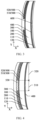
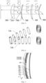
- In order to clearly illustrate the technical solution of the embodiments of the invention, the drawings of the embodiments will be briefly described in the following; it is obvious that the described drawings are only related to some embodiments of the present disclosure and thus are not limitative of the present disclosure.
-
Fig. 1 is a schematic diagram of an optical structure. -
Fig. 2 is a schematic diagram of an optical structure provided according to an example of an embodiment of the present disclosure. -
Fig. 3 is a schematic diagram of an optical structure provided according to another example of an embodiment of the present disclosure. -
Fig. 4 is a schematic diagram of an optical structure provided according to another example of an embodiment of the present disclosure. -
Fig. 5 is a schematic diagram illustrating a folded optical path adopting a phase compensation structure in the optical structure shown inFig. 4 . -
Fig. 6 is a schematic diagram of a polarization state of central light and a polarization state of peripheral light after compensation in the folded optical path shown inFig. 5 . -
Fig. 7 is a schematic diagram of an optical structure provided according to another example of an embodiment of the present disclosure. -
Fig. 8 is a partial structural diagram of a display device according to another embodiment of the present disclosure. - In order to make objects, technical details and advantages of the embodiments of the disclosure apparent, the technical solutions of the embodiments will be described in a clearly and fully understandable way in connection with the drawings related to the embodiments of the disclosure. Apparently, the described embodiments are just a part but not all of the embodiments of the disclosure. Based on the described embodiments herein, those skilled in the art can obtain other embodiment(s), without any inventive work, which should be within the scope of the disclosure.
- Unless otherwise defined, all the technical and scientific terms used herein have the same meanings as commonly understood by one of ordinary skill in the art to which the present disclosure belongs. The terms "first," "second," etc., which are used in the description and the claims of the present disclosure, are not intended to indicate any sequence, amount or importance, but distinguish various components. The terms "comprise," "comprising," "include," "including," etc., are intended to specify that the elements or the objects stated before these terms encompass the elements or the objects and equivalents thereof listed after these terms, but do not preclude the other elements or obj ects.
-
Fig. 1 is a schematic diagram of an optical structure. As shown inFig. 1 , the optical structure includes alens 10, atransflective film 20 located at a side of thelens 10 facing a display screen, aphase retardation film 30 located between thelens 10 and thetransflective film 20, a reflective polarizingfilm 40 located at a side of thephase retardation film 30 away from the display screen, and a linear polarizing film (not shown) located at a side of the reflective polarizingfilm 40 away from the display screen. A light-emitting side of the display screen can be provided with a wave plate, and image light emitted from the display screen is converted into left-handed circularly polarized light after passing through the wave plate, and a polarization state of the left-handed circularly polarized light remains unchanged after being transmitted through thetransflective film 20. For example, thetransflective film 20 allows 50% of a light intensity of incident light to be transmitted therethrough. - During research, inventors of the present application found that when the
phase retardation film 30 is attached onto a curved surface of thelens 10, phase retardation characteristics of thephase retardation film 30 would be affected due to stretching. For example, thephase retardation film 30 includes a birefringent material, and a stretching of thephase retardation film 30 would have an influence on birefringent characteristics thereof, thus affecting a change of polarization state of light in the folded optical path (Pancake). For example, light that is exited from the phase retardation film and supposed to be circularly polarized light may become elliptically polarized light. As a result, the elliptically polarized light cannot be completely converted into linearly polarized light when it reaches the reflective polarizingfilm 40, and the escaped part of the light is referred to as stray light. - As shown in
Fig. 1 , left-handed circularly polarized light transmitted through thetransflective film 20 has a part converted into S-linearly polarized light and another part converted into left-handed elliptically polarized light, after passing through thephase retardation film 30. Thus, a light intensity of the S-linearly polarized light is less than 50%. After transmitting through thelens 10, the above-mentioned S-polarized light reaches the reflective polarizingfilm 40 and is reflected by the reflective polarizingfilm 40, and then reaches thephase retardation film 30 after being transmitted through thelens 10, again. After transmitting through thelens 10, the above-mentioned left-handed elliptically polarized light reaches the reflective polarizingfilm 40, and then light with a partial polarization component in the left-handed elliptically polarized light is reflected by the reflective polarizingfilm 40 while light with another partial polarization component is transmitted by the reflective polarizingfilm 40. - As shown in
Fig. 1 , the S-linearly polarized light is converted into left-handed circularly polarized light after passing through thephase retardation film 30, and the left-handed circularly polarized light is converted into right-handed circularly polarized light after undergoing a half-wave loss at thetransflective film 20. For example, the left-handed circularly polarized light with a light intensity less than 50% remains a light intensity of less than 25% after being reflected by thetransflective film 20. The right-handed circularly polarized light has a part converted into P-linearly polarized light and another part converted into right-handed elliptically polarized light, after passing through thephase retardation film 30. The above-mentioned P-linearly polarized light is exited to human eyes after being transmitted through the reflective polarizing film and a polarization transmission film; and the light with a partial polarization component in the above-mentioned right-handed elliptically polarized light is exited to human eyes after being transmitted through the reflective polarizing film and the polarization transmission film. - The image light emitted from the display screen can also be converted into right-handed circularly polarized light after passing through the wave plate.
- Embodiments of the present disclosure provide an optical structure and a display device. The optical structure includes a lens, a transflective film, a phase retardation film and a reflective polarizing film which are arranged in a stacked manner. The lens includes a first surface and a second surface, both of which are non-planar surfaces; the transflective film is located at a side of the first surface away from the second surface; the phase retardation film is located at a side of the second surface away from the first surface, or between the transflective film and the first surface; and the reflective polarizing film is located at a side of the phase retardation film away from the transflective film. The optical structure further includes a phase compensation structure, which is located between the phase retardation film and the lens or located at a side of the phase retardation film away from the lens. The phase compensation structure includes at least one first light-transmitting layer and at least one second light-transmitting layer which are arranged in a stacked manner, and the at least one first light-transmitting layer and the at least one second light-transmitting layer are alternately arranged; a refractive index of the first light-transmitting layer is greater than that of the second light-transmitting layer; a number of the at least one first light-transmitting layer is equal to that of the at least one second light-transmitting layer; and the first light-transmitting layer is attached with the phase retardation film. By arranging a phase compensation structure attached with a phase retardation film, the optical structure provided by the present disclosure can compensate the elliptically polarized light exited from the phase retardation film having a non-planar shape so that the elliptically polarized light is converted into circularly polarized light, thereby improving polarization conversion efficiency and reducing stray light.
- The optical structure and the display device provided by the embodiments of the present disclosure are described below with reference to the drawings.
-
Fig. 2 is a schematic diagram of an optical structure provided according to an example of an embodiment of the present disclosure. As shown inFig. 2 , the optical structure includes alens 100, atransflective film 200, aphase retardation film 300, and a reflectivepolarizing film 400 which are arranged in a stacked manner. Thelens 100 includes afirst surface 110 and asecond surface 120, both of which are non-planar surfaces. - In some examples, as shown in
Fig. 2 , at least one of thefirst surface 110 and thesecond surface 120 is an aspheric surface or a spherical surface. For example, both thefirst surface 110 and thesecond surface 120 are aspheric surfaces or spherical surfaces; alternatively, one of thefirst surface 110 and thesecond surface 120 is a spherical surface and the other one is an aspheric surface. The optical structure provided by the present disclosure is not limited to this, and the first surface and the second surface may also include free-form surfaces and the like. For example, thelens 100 is a monocle.Fig. 2 schematically shows that thefirst surface 110 is a convex surface and thesecond surface 120 is a concave surface. However, the present disclosure is not limited to this. The first surface can also be a concave surface and the second surface can also be a convex surface; alternatively, both the first surface and the second surface are convex surfaces; alternatively, both the first surface and the second surface are concave surfaces. - For example, the
second surface 120 may be located at a light-emitting side of thefirst surface 110. For example, when the optical structure is applied to a display device, the display screen is located at a side of thefirst surface 110 away from thesecond surface 120 of thelens 100, so that light emitted from the display screen enters thelens 100 after passing through thefirst surface 110, and then exits through thesecond surface 120. - As shown in
Fig. 2 , thetransflective film 200 is located at a side of thefirst surface 110 away from thesecond surface 120. For example, thetransflective film 200 is configured to transmit a part of light and reflect another part of light. For example, thetransflective film 200 may include at least one film layer, for example, a thickness of each film layer may be 10 to 200 nanometers. For example, thetransflective film 200 may have a transmittance of 50% and a reflectivity of 50%. For example, thetransflective film 200 may have a transmittance of 60% and a reflectivity of 40%. For example, thetransflective film 200 may have a transmittance of 65% and a reflectivity of 35%. The optical structure provided by the present disclosure is not limited to this, and the transmittance and reflectivity of the transflective film can be set according to product requirements. For example, when thephase retardation film 300 is located at a side of thesecond surface 120 away from thefirst surface 110, thetransflective film 200 may be plated onto thefirst surface 110. - As shown in
Fig. 2 , thephase retardation film 300 is located at a side of thesecond surface 120 away from thefirst surface 110, or between thetransflective film 200 and thefirst surface 110. In the example shown inFig. 2 , the phase retardation film is located between the transflective film and the first surface, but the embodiment of the present disclosure is not limited to this. In some other examples, the phase retardation film may be located at a side of the second surface away from the first surface. - In some examples, as shown in
Fig. 2 , thephase retardation film 300 includes a quarter-wave plate (QWP). For example, in a case that thephase retardation film 300 is not stretched, linearly polarized light will be converted into circularly polarized light after passing through thephase retardation film 300 at 45 degrees, and the phase will be delayed by 1/4 wavelength (both in the left and right directions). Similarly, circularly polarized light will be converted into linearly polarized light after passing through thephase retardation film 300. For example, thephase retardation film 300 is configured to change the polarized form of the light, so that the light can be smoothly reflected or transmitted by the reflective polarizing film. - For example, as shown in
Fig. 2 , thephase retardation film 300 may be attached onto the non-planarfirst surface 110 to form a non-planar structure, or thephase retardation film 300 may be attached onto the non-planarsecond surface 120 to form a non-planar structure. For example, when thephase retardation film 300 is formed in a planar shape, it is configured such that the light transmitted through thephase retardation film 300 can achieve a conversion between a circular polarization state and a linear polarization state. For example, a material of thephase retardation film 300 may include a plastic film with high light transmittance. For example, thephase retardation film 300 has the following characteristics: there are a direction with the lowest refractive index and a direction with the highest refractive index in the film plane which are referred to as a fast axis and a slow axis, respectively, and the phase of the polarized light parallel to the slow axis is delayed by 1/4 wavelength after passing through thephase retardation film 300, as compared with the polarized light parallel to the fast axis after passing through thephase retardation film 300. - As shown in
Fig. 2 , the reflectivepolarizing film 400 is located at a side of thephase retardation film 300 away from thetransflective film 200. - For example, as shown in
Fig. 2 , the reflectivepolarizing film 400 has the following functions: there is a direction of light transmission axis in the film plane, and a transmittance of a polarized component (e.g., one of the S-linearly polarized light and the P-linearly polarized light) of incident light parallel to the direction of light transmission axis is greater than that of a polarized component of the incident light perpendicular to the direction of light transmission axis, while a reflectivity of the polarized component parallel to the direction of light transmission axis is less than that of the polarized component perpendicular to the direction of light transmission axis. For example, the reflectivepolarizing film 400 can also be referred to as a polarizing beam splitting film. For example, the transmittance of the polarized light parallel to the direction of light transmission axis of the reflectivepolarizing film 400 is not less than 85%, for example, not less than 90%, for example, not less than 95%, for example, not less than 98%; the reflectivity of the polarized light perpendicular to the direction of light transmission axis of the reflectivepolarizing film 400 is not less than 85%, for example, not less than 90%, for example, not less than 95%, for example, not less than 98%. For example, the reflectivepolarizing film 400 may include a liquid crystal polymer film based on cholesteric phase, multilayer reflective polarizing film, metal wire grid polarizer (WGF) and the like. - For example, as shown in
Fig. 2 , an included angle between the slow axis of thephase retardation film 300 and the light transmission axis of the reflectivepolarizing film 400 is 45 degrees. - As shown in
Fig. 2 , the optical structure further includes a phase compensation structure 500, which is located at a side of thephase retardation film 300 away from thelens 100. For example, the phase compensation structure 500 is located between thetransflective film 200 and thephase retardation film 300. The phase compensation structure 500 is attached onto a surface of thephase retardation film 300. - As shown in
Fig. 2 , the phase compensation structure 500 includes at least one first light-transmitting layer 510 and at least one second light-transmitting layer 520 which are arranged in a stacked manner, and the at least one first light-transmitting layer 510 and the at least one second light-transmitting layer 520 are arranged alternately. A refractive index of the first light-transmitting layer 510 is greater than that of the second light-transmitting layer 520, and the number of the at least one first light-transmitting layer 510 is equal to that of the at least one second light-transmitting layer 520. The first light-transmitting layer 510 is attached with thephase retardation film 300. For example, the at least one first light-transmitting layer 510 and the at least one second light-transmitting layer 520 are alternately arranged in a direction parallel to an optical axis of thelens 100, and the optical axis of thelens 100 is parallel to the X direction. - For example,
Fig. 2 schematically shows that the number of the first light-transmitting layer and the number of the second light-transmitting layer are both set as two, but the present disclosure is not limited to this. The number of the first light-transmitting layer and the number of the second light-transmitting layer can also be set as one, or three, or four, or more. - In some examples, as shown in
Fig. 2 , the phase compensation structure 500 is configured to compensate the elliptically polarized light exited from thephase retardation film 300 having a non-planar shape so that the elliptically polarized light is converted into circularly polarized light. - By arranging the phase compensation structure attached with the phase retardation film, the optical structure provided by the present disclosure can compensate the elliptically polarized light exited from the phase retardation film having a non-planar shape so that the elliptically polarized light is converted into circularly polarized light, thereby improving polarization conversion efficiency and reducing stray light.
- For example, the phase compensation structure 500 can be used as another phase retardation structure different from the phase retardation film. The phase compensation structure 500 includes a fast axis and a slow axis. For example, the phase compensation structure 500 can decompose incident, linearly polarized light into an o-light component and an e-light component whose optical vectors are along the fast axis and the slow axis respectively. The phase compensation structure 500 enables two branched of polarized light whose optical vectors are perpendicular to each other to generate a relative phase retardation, in order to optimize an optical path difference between the o-light component and the e-light component which are incident into or exited from the
phase retardation film 300. For example, Jones vector can be used to represent the above-mentioned phase compensation process: Ex=Axcos(ωt), Ey=Aycos(ωt±(δ)±Δδ). A phase difference between the o-light component and the e-light component exited from thephase retardation film 300 can be δ, and a phase difference that can be compensated by the phase compensation structure 500 for the phase difference between the o-light component and the e-light component incident into or exited from thephase retardation film 300 can be Δδ, where δ+Δδ=π/2. Therefore, after stretching a curved surface of the phase retardation film, it causes the o-light component and the e-light component to have a phase difference δ less than π/2, and the phase difference δ generated by the phase retardation film is then compensated by Δδ through the phase compensation structure, so that the phase difference of the light after passing through the phase retardation film and the phase compensation structure reaches π/2. In this way, a mutual conversion between linearly polarized light and circularly polarized light is realized, so as to reduce the stray light generated in the folded optical path of the optical structure. - For example, as shown in
Fig. 2 , the optical structure provided by the present disclosure adopts an ultra-short focus folded optical path (Pancake), and the principle of the folded optical path is as follows: a wave plate can be arranged at a light-emitting side of the display screen located at a side of thefirst surface 110 of thelens 100 away from thesecond surface 120, and image light emitted from the display screen is converted into right-handed circularly polarized light after passing through the wave plate, and a polarization state of the right-handed circularly polarized light remains unchanged after being transmitted through thetransflective film 200. The right-handed circularly polarized light is incident into thephase retardation film 300 and the phase compensation structure 500 and is converted into P-linearly polarized light by thephase retardation film 300 and the phase compensation structure 500, and the P-linearly polarized light is reflected back to thephase retardation film 300 and the phase compensation structure 500 by the reflectivepolarizing film 400, where a first reflection occurs. Then, after passing through thephase retardation film 300 and the phase compensation structure 500, the P-linearly polarized light is converted into right-handed circularly polarized light, which reaches thetransflective film 200 and is reflected at thetransflective film 200, where a second reflection occurs. Due to half-wave loss, the reflected light is converted from right-handed circularly polarized light to left-handed circularly polarized light. The left-handed circularly polarized light is converted into S-linearly polarized light after passing through thephase retardation film 300 and the phase compensation structure 500, and then the S-linearly polarized light is transmitted through the reflectivepolarizing film 400 and emitted to human eyes. - In the above-mentioned folded optical path, different films can be attached onto the same lens or different surfaces of different lenses, or can be superimposed on the same surface of the lens. No matter how the films are attached onto the surface(s) of the lens(es), the arrangement of the optical path and the sequence of positions of the optical films are fixed; for example, the transflective film, the phase retardation film and the reflective polarizing film are arranged, in turn, from the display screen to the human eyes.
- The above-described folded optical path can change the polarization state of the light propagating between the reflective polarizing film and the transflective film and realize the folding of light, so that the original focal length of the optical structure can be folded due to the increase of, for example, two times of reflections resulted by the provision of the reflective polarizing film, the phase retardation film and the transflective film as described above, thereby greatly reducing the space required between human eyes and the optical structure, and achieving a smaller and lighter optical structure.
- In some examples, as shown in
Fig. 2 , a thickness of the phase compensation structure 500 is 0.5-2 microns, a refractive index of the first light-transmitting layer 510 is 1.5-1.9, and a refractive index of the second light-transmitting layer 520 is 1.1-1.4. - The relative phase retardation between two branched of polarized light whose optical vectors are perpendicular to each other, caused by the phase compensation structure, is correlated to the thickness and the refractive index of the phase compensation structure. By configuring the thickness of the phase compensation structure and the refractive indices of various films, the phase difference of the light after passing through the phase retardation film and the phase compensation structure can reach π/2, so as to realize the mutual conversion between linearly polarized light and circularly polarized light.
- For example, as shown in
Fig. 2 , the thickness of the phase compensation structure 500 may be 0.8 to 1.8 microns. For example, the thickness of the phase compensation structure 500 may be 1 to 1.5 microns. For example, the thickness of the first light-transmitting layer 510 may be as same as or different from the thickness of the second light-transmitting layer 520. - For example, as shown in
Fig. 2 , the refractive index of the first light-transmitting layer 510 may be 1.8 to 1.9. For example, the refractive index of the second light-transmitting layer 520 may be 1.2 to 1.3. - In some examples, as shown in
Fig. 2 , materials of the first light-transmitting layer 510 and the second light-transmitting layer 520 are both oxide materials. - In some examples, as shown in
Fig. 2 , the material of the first light-transmitting layer 510 includes at least one of titanium oxide, tantalum oxide and magnesium oxide, and the material of the second light-transmitting layer 520 includes at least one of silicon oxide, aluminum oxide and indium tin oxide. - For example, the material of the first light-transmitting layer 510 includes titanium dioxide (TiO2), titanium monoxide (TiO), titanium pentoxide (Ti2O5), tantalum pentoxide (Ta2O5), magnesium oxide (MgO) and the like. For example, the material of the second light-transmitting layer 520 includes silicon dioxide (SiO2), aluminum trioxide (Al2O3), indium tin oxide (ITO) and the like.
- For example, as shown in
Fig. 2 , the phase compensation structure 500 is attached onto a surface of thephase retardation film 300 having been stretched, to form a non-planar structure, for example, the phase compensation structure 500 has a curved surface. - In some examples, as shown in
Fig. 2 , the phase compensation structure 500 is configured to compensate a phase of light incident thereon, and an incident angle of the light incident on the phase compensation structure 500 is in a range of 50-89 degrees. The above-mentioned incident angle may refer to an angle of light incident on the optical structure with relative to a plane (e.g., an imaginary plane) perpendicular to the optical axis of the lens, and the phase of the light having an included angle of 50-89 degrees with relative to this plane can be compensated. For example, the included angle between the light and the optical axis of thelens 100 can be no more than 40 degrees, that is, the phase of the light having an included angle of no more than 40 degrees with relative to the optical axis of thelens 100 can be compensated. - For example, as shown in
Fig. 2 , the phase compensation structure 500 can compensate the phase of the incident light with an incident angle of 55-85 degrees. For example, the phase compensation structure 500 can compensate the phase of the incident light with an incident angle of 60-80 degrees. For example, the phase compensation structure 500 can compensate the phase of the incident light with an incident angle of 65-75 degrees. - In some examples, as shown in
Fig. 2 , the phase compensation structure 500 is configured to compensate the phase of light incident thereon, and a wavelength range of the light incident on the phase compensation structure 500 is in a range of 350-800 nanometers. The phase compensation structure can compensate the phase of light within a visible band in the incident light, so as to reduce stray light in the visible light band. - In some examples, as shown in
Fig. 2 , thephase retardation film 300 includes acentral region 310 and aperipheral region 320 surrounding thecentral region 310, and the phase compensation structure 500 covers theperipheral region 320 of thephase retardation film 300, and a ratio of an area of thecentral region 310 to an area of thephase retardation film 300 is not more than 50%. Here, "the ratio of the area of thecentral region 310 to the area of thephase retardation film 300" refers to an area ratio of the central region occupied on one side surface of the phase retardation film. - For example, the phase compensation structure 500 is only located in the
peripheral region 320, and the phase compensation structure 500 does not overlap with thecentral region 310 in a direction parallel to the optical axis of thelens 100. - The central region of the phase retardation film having a non-planar shape is stretched lightly so that phase retardation characteristics of this part of the phase retardation film are hardly affected; while the peripheral region of the phase retardation film having a non-planar shape is stretched heavily, which seriously affects the phase retardation characteristics thereof. The phase compensation structure is intentionally arranged in the peripheral region of the corresponding phase retardation film to compensate the elliptically polarized light exited from the peripheral region of the phase retardation film so that the elliptically polarized light is converted into circularly polarized light, but the phase compensation structure is not arranged in the central region of the phase retardation film; in this way, the phase compensation structure can compensate the phase retardation characteristics of the phase retardation film in a better way.
- For example, as shown in
Fig. 2 , thecentral region 310 of thephase retardation film 300 is a region including a center of thephase retardation film 300; thecentral region 310 may be a circular region with the center of thephase retardation film 300 as a center of circle, and theperipheral region 320 may be an annular region surrounding thecentral region 310. - For example, as shown in
Fig. 2 , the ratio of the area of thecentral region 310 to the area of thephase retardation film 300 is not more than 45%. For example, the ratio of the area of thecentral region 310 to the area of thephase retardation film 300 is not more than 40%. For example, the ratio of the area of thecentral region 310 to the area of thephase retardation film 300 is not more than 35%. For example, the ratio of the area of thecentral region 310 to the area of thephase retardation film 300 is not less than 30%. For example, the ratio of the area of thecentral region 310 to the area of thephase retardation film 300 is not more than 25%. For example, the ratio of the area of thecentral region 310 to the area of thephase retardation film 300 is not more than 20%. For example, the ratio of the area of thecentral region 310 to the area of thephase retardation film 300 is not more than 15%. For example, the ratio of the area of thecentral region 310 to the area of thephase retardation film 300 is not more than 10%. - In some examples, as shown in
Fig. 2 , a curvature of one of thefirst surface 110 and thesecond surface 120 of thelens 100 on which thephase retardation film 300 is provided is not less than 30 millimeters, and thecentral region 310 surrounded by the phase compensation structure 500 is provided with a light-transmitting structure, and the light-transmitting structure is a part of one of thephase retardation film 300, thetransflective film 200 and the reflectivepolarizing film 400 which fills thecentral region 310. - For example,
Fig. 2 schematically shows that the phase compensation structure 500 is located between thetransflective film 200 and thephase retardation film 300, and thetransflective film 200 covers the phase compensation structure 500, so that thetransflective film 200 fills thecentral region 310 surrounded by the phase compensation structure 500. The embodiment of the present disclosure is not limited to this. When the phase compensation structure is located between the phase retardation film and the lens, the phase retardation film covers the phase compensation structure, and the phase retardation film can fill the central region surrounded by the phase compensation structure. Alternatively, when the phase compensation structure is located between the phase retardation film and the reflective polarizing film, the reflective polarizing film covers the phase compensation structure, and the reflective polarizing film can fill the central region surrounded by the phase compensation structure. - For example, in a case that the
phase retardation film 300 is attached onto thefirst surface 110 and the curvature of thefirst surface 110 is not less than 30 millimeters, the phase compensation structure 500 covers theperipheral region 320 of thephase retardation film 300; alternatively, in a case that thephase retardation film 300 is attached onto thesecond surface 120 and the curvature of thesecond surface 120 is not less than 30 millimeters, the phase compensation structure 500 covers theperipheral region 320 of thephase retardation film 300. - When the curvature of the non-planar surface of the lens provided with the phase retardation film is not less than 30 millimeters, there is little difference between the brightness of the light exited after passing through the peripheral region of the phase retardation film and the phase retardation film and the brightness of the light exited after passing through the central region of the phase retardation film only, and the central region of the phase retardation film may not be provided with any other film for optical compensation.
-
Fig. 3 is a schematic diagram of an optical structure provided according to another example of an embodiment of the present disclosure. The optical structure shown inFig. 3 is different from the optical structure shown inFig. 2 in that the optical structure shown inFig. 3 further includes a linearpolarizing film 600, which is located at a side of the reflectivepolarizing film 400 away from thephase retardation film 300. - For example, as shown in
Fig. 3 , a transmission axis of the linearpolarizing film 600 coincides with a transmission axis of the reflectivepolarizing film 400. For example, the linearpolarizing film 600 is configured to further filter out other stray light, so that only polarized light (e.g., one of S-linearly polarized light and P-linearly polarized light) passing through the linearpolarizing film 600 is allowed to enter human eyes. For example, a material of the linearpolarizing film 600 may include polyvinyl alcohol (PVA) added with dichroic molecules, a liquid crystal polymer film added with dichroic molecules, and the like. - For example, as shown in
Fig. 3 , the reflectivepolarizing film 400 can be attached onto thesecond surface 120 of thelens 100, and the linearpolarizing film 600 can be attached onto a surface of the reflectivepolarizing film 400. -
Fig. 4 is a schematic diagram of an optical structure provided according to another example of an embodiment of the present disclosure. The optical structure shown inFig. 4 is different from the optical structure shown inFig. 2 in that the curvature of the surface of thelens 100 provided with thephase retardation film 300 is less than 30 millimeters, and the optical structure further includes a third light-transmittinglayer 530. - In some examples, as shown in
Fig. 4 , the curvature of one of thefirst surface 110 and thesecond surface 120 of thelens 100 on which thephase retardation film 300 is provided is less than 30 millimeters. For example,Fig. 4 schematically shows that thephase retardation film 300 is attached onto thefirst surface 110 of thelens 100, and the curvature of thefirst surface 110 is less than 30 millimeters, without limiting the present disclosure thereto. The phase retardation film can also be attached onto the second surface of the lens, and the curvature of the second surface is less than 30 millimeters. - In some examples, as shown in
Fig. 4 , the optical structure further includes a third light-transmittinglayer 530 located in thecentral region 310. The third light-transmittinglayer 530 is arranged at the same layer as the phase compensation structure 500 and is connected with the phase compensation structure 500, and a transmittance of the third light-transmittinglayer 530 is different from that of the phase compensation structure 500. For example, in the direction along the optical axis of thelens 100, the third light-transmittinglayer 530 does not overlap with the phase compensation structure 500. - When the surface of the lens provided with the phase retardation film has a curvature less than 30 millimeters, there will be a certain difference between the brightness of the light exited after passing through the peripheral region of the phase retardation film and the phase compensation structure and the brightness of the light exited after passing through the central region of the phase retardation film only. For example, the brightness of the central region is greater than that of the peripheral region. By arranging the third light-transmitting layer in the central region of the phase retardation film, and by configuring the transmittance of the third light-transmitting layer to be different from that of the phase compensation structure, it is beneficial to reduce the brightness difference between the light exited from the central region and the light exited from the peripheral region and to prevent from the occurrence of visual sudden waves.
- By arranging the phase compensation structure and the third light-transmitting layer at the same side of the phase retardation film, the brightness difference of the light exited from different positions of the phase retardation film can be reduced while the phase compensation is carried out to the light exited from the phase retardation film.
- For example, as shown in
Fig. 4 , the phase compensation structure 500 surrounds the third light-transmittinglayer 530. - In some examples, as shown in
Fig. 4 , the transmittance of the third light-transmittinglayer 530 is smaller than that of the phase compensation structure 500, which is beneficial to reduce the brightness of light exited from the central region of the phase retardation film. - In some examples, as shown in
Fig. 4 , a difference between the transmittance of the third light-transmittinglayer 530 and the transmittance of the phase compensation structure 500 is not more than 5% of the transmittance of the phase compensation structure 500. For example, the difference between the transmittance of the third light-transmittinglayer 530 and the transmittance of the phase compensation structure 500 is not more than 3% of the transmittance of the phase compensation structure 500. The difference between the transmittance of the third light-transmitting layer and the transmittance of the phase compensation structure can be determined according to the difference between the brightness of the light exited from the central region of the phase retardation film and the brightness of the light exited from the peripheral region of the phase retardation film, so as to alleviate the brightness difference. - In some examples, as shown in
Fig. 4 , at least part of a surface of the third light-transmittinglayer 530 away from thelens 100 is recessed with relative to the surface of the phase compensation structure 500 away from thelens 100. - For example, as shown in
Fig. 4 , a thickness of the third light-transmittinglayer 530 is smaller than that of the phase compensation structure 500. - For example, as shown in
Fig. 4 , the thickness of the third light-transmittinglayer 530 is less than 2 microns. For example, the thickness of the third light-transmittinglayer 530 is less than 1.8 microns. For example, the thickness of the third light-transmittinglayer 530 is less than 1.5 microns. For example, the thickness of the third light-transmittinglayer 530 is less than 1 micron. For example, the thickness of the third light-transmittinglayer 530 is less than 0.7 micron. For example, the thickness of the third light-transmittinglayer 530 is less than 0.5 micron. For example, the thickness of the third light-transmittinglayer 530 is less than 0.4 micron. - In some examples, as shown in
Fig. 4 , a surface at a position where the third light-transmittinglayer 530 is connected with the phase compensation structure 500 is recessed with relative to a surface at a position where the phase compensation structure 500 is connected with the third light-transmittinglayer 530, and a recessed depth is smaller than the thickness of thephase retardation film 300. - For example, as shown in
Fig. 4 , a thickness difference between the phase compensation structure 500 and the third light-transmittinglayer 530 is smaller than the thickness of thephase retardation film 300, so as to prevent from affecting the optical performance of the film (e.g., the phase retardation film or the transflective film) covering the phase compensation structure and the third light-transmitting layer. - In some examples, as shown in
Fig. 4 , the third light-transmittinglayer 530 includes a metal dielectric film or a reflective dielectric film. For example, a material of the metal dielectric film may include metals such as silver. For example, a material of the reflective dielectric film may include metal oxides, such as zinc oxide, aluminum oxide, etc. - The optical structure provided by the present disclosure can reduce the brightness difference between light exited from the central region of the phase retardation film and light exited from the peripheral region of the phase retardation film, by selecting the thickness and material of the third transparent layer.
- For example,
Figs. 1 to 4 schematically show that thetransflective film 200, the phase compensation structure 500 and thephase retardation film 300 are all arranged on thefirst surface 110 of thelens 100, and the reflectivepolarizing film 400 is arranged on thesecond surface 120 of thelens 100. The embodiment of the present disclosure is not limited to this. For example, the transflective film can be arranged on the first surface of the lens, and the phase compensation structure, the phase retardation film and the reflective polarizing film can be arranged on the second surface of the lens. Alternatively, the transflective film can be arranged on the first surface of the lens, the phase compensation structure and the phase retardation film can be arranged on the second surface of the lens, and the reflective polarizing film can be arranged on the surface of another lens. -
Fig. 5 is a schematic diagram illustrating a folded optical path using the phase compensation structure in the optical structure shown inFig. 4 .Fig. 6 is a schematic diagram of a polarization state of central light and a polarization state of peripheral light after compensation in the folded optical path shown inFig. 5 . As shown inFigs. 4 to 6 , light 710 exited from theperipheral region 320 of thephase retardation film 300 is circularly polarized or approximately circularly polarized after being compensated by the phase compensation structure 500, and light 720 exited from thecentral region 310 of thephase retardation film 300 is circularly polarized light. - For example, as shown in
Figs. 5 and 6 , the image light emitted from the display screen is converted into left-handed circularly polarized light after passing through the wave plate, and the polarization state of the left-handed circularly polarized light remains unchanged after being transmitted through thetransflective film 200. For example, thetransflective film 200 allows 50% of light intensity to be transmitted. The left-handed circularly polarized light transmitted by thetransflective film 200 has a part converted into S-linearly polarized light after passing through the central region of thephase retardation film 300, and another part converted into S-linearly polarized light after passing through the peripheral region of thephase retardation film 300 and the phase compensation structure 500, and a light intensity of the converted S-linearly polarized light is still substantially 50% of a light intensity of the incident light. The above-mentioned S-polarized light reaches the reflectivepolarizing film 400 after being transmitted by thelens 100, and then is reflected by the reflectivepolarizing film 400 and reaches thephase retardation film 300 after being transmitted by thelens 100 again. A part of the S-linearly polarized light passes through the peripheral region of thephase retardation film 300 and the phase compensation structure 500 and is converted into left-handed circularly polarized light, while another part of the S-linearly polarized light passes through the central region of thephase retardation film 300 and is converted into left-handed circularly polarized light. The left-handed circularly polarized light undergoes a half-wave loss at thetransflective film 200 and is converted into right-handed circularly polarized light. For example, a light intensity of the right-handed circularly polarized light, after being reflected by thetransflective film 200, is 25% of the light intensity of the incident light. A part of the right-handed circularly polarized light passes through the peripheral region of thephase retardation film 300 and the phase compensation structure 500 and is converted into P-linearly polarized light, and another part of the right-handed circularly polarized light passes through the central region of thephase retardation film 300 and is converted into P-linearly polarized light. The P-linearly polarized light passes through the reflectivepolarizing film 400 and is exited to human eyes. -
Fig. 7 is a schematic diagram of an optical structure provided according to another example of an embodiment of the present disclosure. The optical structure shown inFig. 7 is different from the optical structure shown inFig. 4 in that the phase compensation structure 500 is located between thephase retardation film 300 and thelens 100. The characteristics of various films in the optical structure shown inFig. 7 are the same as those of various films in the optical structure shown inFig. 4 , and will not be described here. -
Fig. 8 is a partial structural diagram of a display device according to another embodiment of the present disclosure. As shown inFig. 8 , the display device includes adisplay screen 020 and the optical structure shown in any of the above embodiments. Thedisplay screen 020 is located at a side of thefirst surface 110 away from thesecond surface 120. The optical structure schematically shown inFig. 8 is the optical structure shown inFig. 4 , but the present disclosure is not limited thereto, and the optical structure in the display device can also be the optical structure in other examples described above. - For example, as shown in
Fig. 8 , a display surface of thedisplay screen 020 is located at a focal plane of the light incident side of the optical structure. - For example, the
display screen 020 can be any type of display screen, such as a liquid crystal display screen, an organic light emitting diode display screen, an inorganic light emitting diode display screen, a quantum dot display screen, a projector (such as an LCOS micro projector), and the like. - For example, the display device may be a virtual reality (VR) display device. For example, the virtual reality display device can be a display device adopting an ultra-short focus folded optical path.
- For example, the display device may be a near-eye display device, which may be a wearable VR helmet, VR glasses, etc., and embodiments of the present disclosure are not limited thereto.
- The following statements should be noted:
- (1) In the accompanying drawings of the embodiments of the present disclosure, the drawings involve only the structure(s) in connection with the embodiment(s) of the present disclosure, and other structure(s) can be referred to common design(s).
- (2) In case of no conflict, features in one embodiment or in different embodiments can be combined.
- What have been described above are only specific implementations of the present disclosure, the protection scope of the present disclosure is not limited thereto, and the protection scope of the present disclosure should be based on the protection scope of the claims.
Claims (15)
- An optical structure, comprising:a lens (100), comprising a first surface (110) and a second surface (120), wherein both the first surface (110) and the second surface (120) are non-planar surfaces;a transflective film (200), located at a side of the first surface (110) away from the second surface (120);a phase retardation film (300), located at a side of the second surface (120) away from the first surface (110) or located between the transflective film (200) and the first surface (110); anda reflective polarizing film (400), located at a side of the phase retardation film (300) away from the transflective film (200), whereinthe optical structure further comprises a phase compensation structure (500) which is located between the phase retardation film (300) and the lens (100) or located at a side of the phase retardation film (300) away from the lens (100), and the phase compensation structure (500) comprises at least one first light-transmitting layer (510) and at least one second light-transmitting layer (520) which are arranged in a stacked manner, wherein the at least one first light-transmitting layer (510) and the at least one second light-transmitting layer (520) are alternately arranged, and a refractive index of the first light-transmitting layer (510) is greater than a refractive index of the second light-transmitting layer (520), and a number of the at least one first light-transmitting layer (510) is equal to a number of the at least one second light-transmitting layer (520); and the first light-transmitting layer (510) is attached with the phase retardation film (300).
- The optical structure according to claim 1, wherein the phase retardation film (300) comprises a central region (310) and a peripheral region (320) surrounding the central region (310), the phase compensation structure (500) covers the peripheral region (320) of the phase retardation film (300), and a ratio of an area of the central region (310) to an area of the phase retardation film (300) is not more than 50%.
- The optical structure according to claim 2, whereinone of the first surface (110) and the second surface (120) on which the phase retardation film (300) is arranged has a curvature not less than 30 millimeters, andthe central region (310) is provided with a light-transmitting structure, and the light-transmitting structure is a part of one of the phase retardation film (300), the transflective film (200) and the reflective polarizing film (400) which fills the central region (310).
- The optical structure according to claim 2, wherein one of the first surface (110) and the second surface (120) on which the phase retardation film (300) is arranged has a curvature less than 30 millimeters;
the optical structure further comprises a third light-transmitting layer (530) located in the central region (310), the third light-transmitting layer (530) is arranged at the same layer as the phase compensation structure (500) and is connected with the phase compensation structure (500), and a transmittance of the third light-transmitting layer (530) is different from a transmittance of the phase compensation structure (500). - The optical structure according to claim 4, wherein a difference between the transmittance of the third light-transmitting layer (530) and the transmittance of the phase compensation structure (500) is not more than 5% of the transmittance of the phase compensation structure (500).
- The optical structure according to claim 4, wherein the transmittance of the third light-transmitting layer (530) is smaller than the transmittance of the phase compensation structure (500).
- The optical structure according to claim 4, wherein at least part of a surface of the third light-transmitting layer (530) away from the lens (100) is recessed relative to a surface of the phase compensation structure (500) away from the lens (100).
- The optical structure according to claim 7, wherein a surface at a position where the third light-transmitting layer (530) is connected with the phase compensation structure (500) is recessed with relative to a surface at a position where the phase compensation structure (500) is connected with the third light-transmitting layer (530), and a recessed depth is smaller than a thickness of the phase retardation film (300).
- The optical structure according to any one of claims 1-8, wherein a thickness of the phase compensation structure (500) is 0.5-2 microns, the refractive index of the first light-transmitting layer (510) is 1.5-1.9, and the refractive index of the second light-transmitting layer (520) is 1.1-1.4.
- The optical structure according to any one of claims 1-9, wherein the phase compensation structure (500) is configured to compensate a phase of light incident on the phase compensation structure (500), and an incident angle of the light incident on the phase compensation structure (500) is 50 to 89 degrees.
- The optical structure according to any one of claims 1-10, wherein the phase compensation structure (500) is configured to compensate a phase of light incident on the phase compensation structure (500), and a wavelength range of the light incident on the phase compensation structure (500) is 350 to 800 nanometers.
- The optical structure according to any one of claims 2-8, wherein the phase retardation film (300) comprises a quarter-wave plate, the phase retardation film (300) has a non-planar structure, and the phase compensation structure (500) is configured to compensate elliptically polarized light exited from the peripheral region (320) of the phase retardation film (300) so that the elliptically polarized light is converted into circularly polarized light.
- The optical structure according to any one of claims 1-12, whereinmaterials of the first light-transmitting layer (510) and the second light-transmitting layer (520) are both oxide materials, or the material of the first light-transmitting layer (510) comprises a liquid crystal material; optionally,the material of the first light-transmitting layer (510) comprises at least one of titanium oxide, tantalum oxide and magnesium oxide, and the material of the second light-transmitting layer (520) comprises at least one of silicon oxide, aluminum oxide and indium tin oxide.
- The optical structure according to any one of claims 4-8, wherein the third light-transmitting layer (530) comprises a metal dielectric film or a reflective dielectric film.
- A display device, comprising a display screen (020) and the optical structure according to any one of claims 1-14, wherein the display screen (020) is located at a side of the first surface (110) away from the second surface (120).
Applications Claiming Priority (1)
| Application Number | Priority Date | Filing Date | Title |
|---|---|---|---|
| CN202310300554.2A CN118688958A (en) | 2023-03-24 | 2023-03-24 | Optical structure and display device |
Publications (3)
| Publication Number | Publication Date |
|---|---|
| EP4435495A1 true EP4435495A1 (en) | 2024-09-25 |
| EP4435495C0 EP4435495C0 (en) | 2025-11-05 |
| EP4435495B1 EP4435495B1 (en) | 2025-11-05 |
Family
ID=90366762
Family Applications (1)
| Application Number | Title | Priority Date | Filing Date |
|---|---|---|---|
| EP24164220.6A Active EP4435495B1 (en) | 2023-03-24 | 2024-03-18 | Optical structure and display device |
Country Status (3)
| Country | Link |
|---|---|
| US (1) | US20240319426A1 (en) |
| EP (1) | EP4435495B1 (en) |
| CN (1) | CN118688958A (en) |
Citations (3)
| Publication number | Priority date | Publication date | Assignee | Title |
|---|---|---|---|---|
| US20200284963A1 (en) * | 2017-10-25 | 2020-09-10 | 3M Innovative Properties Company | Optical retarder segements |
| US20220099988A1 (en) * | 2020-09-30 | 2022-03-31 | Shanghai UROptics Co. Ltd. | Optical module, near-eye display device and light projection method |
| US20220350148A1 (en) * | 2021-04-29 | 2022-11-03 | Meta Platforms Technologies, Llc | High efficiency pancake lens |
-
2023
- 2023-03-24 CN CN202310300554.2A patent/CN118688958A/en active Pending
-
2024
- 2024-03-18 EP EP24164220.6A patent/EP4435495B1/en active Active
- 2024-03-19 US US18/609,764 patent/US20240319426A1/en active Pending
Patent Citations (3)
| Publication number | Priority date | Publication date | Assignee | Title |
|---|---|---|---|---|
| US20200284963A1 (en) * | 2017-10-25 | 2020-09-10 | 3M Innovative Properties Company | Optical retarder segements |
| US20220099988A1 (en) * | 2020-09-30 | 2022-03-31 | Shanghai UROptics Co. Ltd. | Optical module, near-eye display device and light projection method |
| US20220350148A1 (en) * | 2021-04-29 | 2022-11-03 | Meta Platforms Technologies, Llc | High efficiency pancake lens |
Also Published As
| Publication number | Publication date |
|---|---|
| EP4435495C0 (en) | 2025-11-05 |
| CN118688958A (en) | 2024-09-24 |
| EP4435495B1 (en) | 2025-11-05 |
| US20240319426A1 (en) | 2024-09-26 |
Similar Documents
| Publication | Publication Date | Title |
|---|---|---|
| TWI685682B (en) | Optical film, optical element and imaging device | |
| CN211878327U (en) | Near-to-eye display device and glasses | |
| CN215986726U (en) | Augmented reality display system | |
| CN110161687A (en) | AR display device and wearable AR equipment | |
| TW202303223A (en) | Display system | |
| CN114144716B (en) | Optical system for displaying magnified virtual image | |
| TWI813318B (en) | Head-mounted display | |
| CN110161685A (en) | AR display device and wearable AR equipment | |
| CN110161683A (en) | Image projection apparatus and AR show equipment | |
| CN113448085B (en) | Near-eye display device and glasses | |
| JP2024080627A (en) | Display Module | |
| CN115657305A (en) | AR display device and wearable AR equipment | |
| US20250306375A1 (en) | Optical waveguide structure and head mounted display | |
| EP4435495B1 (en) | Optical structure and display device | |
| US20250102854A1 (en) | Optical system and display apparatus | |
| CN110161684A (en) | AR imaging device and wearable AR equipment | |
| JP7771435B2 (en) | Optical system and display device | |
| CN117666128A (en) | a display device | |
| JP7830715B2 (en) | Optical systems and image display devices | |
| CN221175140U (en) | An optical system | |
| US12092827B2 (en) | Lens of head-mounted display | |
| US20260098992A1 (en) | Optical system and display apparatus | |
| EP4528359A1 (en) | Optical structure and display device | |
| US20250013062A1 (en) | Lens assembly, display module, and electronic device | |
| CN119556470A (en) | Folded optical path lens, optical imaging system and head mounted display device |
Legal Events
| Date | Code | Title | Description |
|---|---|---|---|
| PUAI | Public reference made under article 153(3) epc to a published international application that has entered the european phase |
Free format text: ORIGINAL CODE: 0009012 |
|
| STAA | Information on the status of an ep patent application or granted ep patent |
Free format text: STATUS: REQUEST FOR EXAMINATION WAS MADE |
|
| 17P | Request for examination filed |
Effective date: 20240318 |
|
| AK | Designated contracting states |
Kind code of ref document: A1 Designated state(s): AL AT BE BG CH CY CZ DE DK EE ES FI FR GB GR HR HU IE IS IT LI LT LU LV MC ME MK MT NL NO PL PT RO RS SE SI SK SM TR |
|
| GRAP | Despatch of communication of intention to grant a patent |
Free format text: ORIGINAL CODE: EPIDOSNIGR1 |
|
| STAA | Information on the status of an ep patent application or granted ep patent |
Free format text: STATUS: GRANT OF PATENT IS INTENDED |
|
| RIC1 | Information provided on ipc code assigned before grant |
Ipc: G02B 27/28 20060101ALN20250513BHEP Ipc: G02B 5/30 20060101ALN20250513BHEP Ipc: G02B 27/01 20060101AFI20250513BHEP |
|
| RIC1 | Information provided on ipc code assigned before grant |
Ipc: G02B 27/28 20060101ALN20250519BHEP Ipc: G02B 5/30 20060101ALN20250519BHEP Ipc: G02B 27/01 20060101AFI20250519BHEP |
|
| INTG | Intention to grant announced |
Effective date: 20250602 |
|
| GRAS | Grant fee paid |
Free format text: ORIGINAL CODE: EPIDOSNIGR3 |
|
| GRAA | (expected) grant |
Free format text: ORIGINAL CODE: 0009210 |
|
| STAA | Information on the status of an ep patent application or granted ep patent |
Free format text: STATUS: THE PATENT HAS BEEN GRANTED |
|
| AK | Designated contracting states |
Kind code of ref document: B1 Designated state(s): AL AT BE BG CH CY CZ DE DK EE ES FI FR GB GR HR HU IE IS IT LI LT LU LV MC ME MK MT NL NO PL PT RO RS SE SI SK SM TR |
|
| REG | Reference to a national code |
Ref country code: CH Ref legal event code: F10 Free format text: ST27 STATUS EVENT CODE: U-0-0-F10-F00 (AS PROVIDED BY THE NATIONAL OFFICE) Effective date: 20251105 Ref country code: GB Ref legal event code: FG4D |
|
| REG | Reference to a national code |
Ref country code: DE Ref legal event code: R096 Ref document number: 602024001132 Country of ref document: DE |
|
| REG | Reference to a national code |
Ref country code: IE Ref legal event code: FG4D |
|
| U01 | Request for unitary effect filed |
Effective date: 20251120 |
|
| U07 | Unitary effect registered |
Designated state(s): AT BE BG DE DK EE FI FR IT LT LU LV MT NL PT RO SE SI Effective date: 20251125 |
|
| U20 | Renewal fee for the european patent with unitary effect paid |
Year of fee payment: 3 Effective date: 20260303 |
|
| PG25 | Lapsed in a contracting state [announced via postgrant information from national office to epo] |
Ref country code: ES Free format text: LAPSE BECAUSE OF FAILURE TO SUBMIT A TRANSLATION OF THE DESCRIPTION OR TO PAY THE FEE WITHIN THE PRESCRIBED TIME-LIMIT Effective date: 20251105 |
|
| PG25 | Lapsed in a contracting state [announced via postgrant information from national office to epo] |
Ref country code: NO Free format text: LAPSE BECAUSE OF FAILURE TO SUBMIT A TRANSLATION OF THE DESCRIPTION OR TO PAY THE FEE WITHIN THE PRESCRIBED TIME-LIMIT Effective date: 20260205 |
|
| PG25 | Lapsed in a contracting state [announced via postgrant information from national office to epo] |
Ref country code: HR Free format text: LAPSE BECAUSE OF FAILURE TO SUBMIT A TRANSLATION OF THE DESCRIPTION OR TO PAY THE FEE WITHIN THE PRESCRIBED TIME-LIMIT Effective date: 20251105 |
|
| PG25 | Lapsed in a contracting state [announced via postgrant information from national office to epo] |
Ref country code: RS Free format text: LAPSE BECAUSE OF FAILURE TO SUBMIT A TRANSLATION OF THE DESCRIPTION OR TO PAY THE FEE WITHIN THE PRESCRIBED TIME-LIMIT Effective date: 20260205 |
|
| PG25 | Lapsed in a contracting state [announced via postgrant information from national office to epo] |
Ref country code: IS Free format text: LAPSE BECAUSE OF FAILURE TO SUBMIT A TRANSLATION OF THE DESCRIPTION OR TO PAY THE FEE WITHIN THE PRESCRIBED TIME-LIMIT Effective date: 20260305 |
|
| PG25 | Lapsed in a contracting state [announced via postgrant information from national office to epo] |
Ref country code: PL Free format text: LAPSE BECAUSE OF FAILURE TO SUBMIT A TRANSLATION OF THE DESCRIPTION OR TO PAY THE FEE WITHIN THE PRESCRIBED TIME-LIMIT Effective date: 20251105 |
|
| U1N | Appointed representative for the unitary patent procedure changed after the registration of the unitary effect |
Representative=s name: MARKS & CLERK LLP; GB |