EP4432808A1 - Perovskite solar cell, thin film composite electrode and preparation method, power generation apparatus, and electric apparatus - Google Patents
Perovskite solar cell, thin film composite electrode and preparation method, power generation apparatus, and electric apparatus Download PDFInfo
- Publication number
- EP4432808A1 EP4432808A1 EP22923418.2A EP22923418A EP4432808A1 EP 4432808 A1 EP4432808 A1 EP 4432808A1 EP 22923418 A EP22923418 A EP 22923418A EP 4432808 A1 EP4432808 A1 EP 4432808A1
- Authority
- EP
- European Patent Office
- Prior art keywords
- layer
- metal layer
- transport layer
- conductive oxide
- charge transport
- Prior art date
- Legal status (The legal status is an assumption and is not a legal conclusion. Google has not performed a legal analysis and makes no representation as to the accuracy of the status listed.)
- Pending
Links
- 239000002131 composite material Substances 0.000 title claims abstract description 100
- 239000010409 thin film Substances 0.000 title claims abstract description 99
- 238000002360 preparation method Methods 0.000 title claims abstract description 33
- 238000010248 power generation Methods 0.000 title abstract description 4
- 229910052751 metal Inorganic materials 0.000 claims abstract description 238
- 239000002184 metal Substances 0.000 claims abstract description 238
- 239000011521 glass Substances 0.000 claims abstract description 25
- 230000005525 hole transport Effects 0.000 claims description 21
- 238000001704 evaporation Methods 0.000 claims description 15
- 230000008020 evaporation Effects 0.000 claims description 15
- 239000010931 gold Substances 0.000 claims description 14
- BQCADISMDOOEFD-UHFFFAOYSA-N Silver Chemical compound [Ag] BQCADISMDOOEFD-UHFFFAOYSA-N 0.000 claims description 12
- PCHJSUWPFVWCPO-UHFFFAOYSA-N gold Chemical compound [Au] PCHJSUWPFVWCPO-UHFFFAOYSA-N 0.000 claims description 12
- 229910052737 gold Inorganic materials 0.000 claims description 12
- 229910052709 silver Inorganic materials 0.000 claims description 12
- 239000004332 silver Substances 0.000 claims description 12
- 238000004768 lowest unoccupied molecular orbital Methods 0.000 claims description 11
- PXHVJJICTQNCMI-UHFFFAOYSA-N Nickel Chemical compound [Ni] PXHVJJICTQNCMI-UHFFFAOYSA-N 0.000 claims description 10
- 238000004770 highest occupied molecular orbital Methods 0.000 claims description 10
- 239000010949 copper Substances 0.000 claims description 9
- RYGMFSIKBFXOCR-UHFFFAOYSA-N Copper Chemical compound [Cu] RYGMFSIKBFXOCR-UHFFFAOYSA-N 0.000 claims description 8
- XEEYBQQBJWHFJM-UHFFFAOYSA-N Iron Chemical compound [Fe] XEEYBQQBJWHFJM-UHFFFAOYSA-N 0.000 claims description 8
- 229910045601 alloy Inorganic materials 0.000 claims description 8
- 239000000956 alloy Substances 0.000 claims description 8
- 229910052782 aluminium Inorganic materials 0.000 claims description 8
- XAGFODPZIPBFFR-UHFFFAOYSA-N aluminium Chemical compound [Al] XAGFODPZIPBFFR-UHFFFAOYSA-N 0.000 claims description 8
- 229910052802 copper Inorganic materials 0.000 claims description 8
- 238000004544 sputter deposition Methods 0.000 claims description 8
- 238000001816 cooling Methods 0.000 claims description 7
- 238000007738 vacuum evaporation Methods 0.000 claims description 6
- 230000001174 ascending effect Effects 0.000 claims description 5
- 229910017052 cobalt Inorganic materials 0.000 claims description 5
- 239000010941 cobalt Substances 0.000 claims description 5
- GUTLYIVDDKVIGB-UHFFFAOYSA-N cobalt atom Chemical compound [Co] GUTLYIVDDKVIGB-UHFFFAOYSA-N 0.000 claims description 5
- 229910052759 nickel Inorganic materials 0.000 claims description 5
- ATJFFYVFTNAWJD-UHFFFAOYSA-N Tin Chemical compound [Sn] ATJFFYVFTNAWJD-UHFFFAOYSA-N 0.000 claims description 4
- HCHKCACWOHOZIP-UHFFFAOYSA-N Zinc Chemical compound [Zn] HCHKCACWOHOZIP-UHFFFAOYSA-N 0.000 claims description 4
- 229910052742 iron Inorganic materials 0.000 claims description 4
- 239000011135 tin Substances 0.000 claims description 4
- 229910052718 tin Inorganic materials 0.000 claims description 4
- 229910052725 zinc Inorganic materials 0.000 claims description 4
- 239000011701 zinc Substances 0.000 claims description 4
- 229910052774 Proactinium Inorganic materials 0.000 claims description 3
- 238000000605 extraction Methods 0.000 abstract description 8
- 238000005215 recombination Methods 0.000 abstract description 7
- 230000006798 recombination Effects 0.000 abstract description 7
- 239000000969 carrier Substances 0.000 abstract 2
- 238000010521 absorption reaction Methods 0.000 abstract 1
- 239000000463 material Substances 0.000 description 23
- 229910003437 indium oxide Inorganic materials 0.000 description 18
- PJXISJQVUVHSOJ-UHFFFAOYSA-N indium(iii) oxide Chemical compound [O-2].[O-2].[O-2].[In+3].[In+3] PJXISJQVUVHSOJ-UHFFFAOYSA-N 0.000 description 18
- 239000002800 charge carrier Substances 0.000 description 15
- XOLBLPGZBRYERU-UHFFFAOYSA-N tin dioxide Chemical compound O=[Sn]=O XOLBLPGZBRYERU-UHFFFAOYSA-N 0.000 description 13
- XLOMVQKBTHCTTD-UHFFFAOYSA-N Zinc monoxide Chemical compound [Zn]=O XLOMVQKBTHCTTD-UHFFFAOYSA-N 0.000 description 12
- 238000006243 chemical reaction Methods 0.000 description 12
- 230000000052 comparative effect Effects 0.000 description 12
- 239000002904 solvent Substances 0.000 description 9
- 238000002834 transmittance Methods 0.000 description 9
- KFZMGEQAYNKOFK-UHFFFAOYSA-N Isopropanol Chemical compound CC(C)O KFZMGEQAYNKOFK-UHFFFAOYSA-N 0.000 description 8
- 238000010586 diagram Methods 0.000 description 8
- -1 poly(3,4-ethylenedioxythiophene) Polymers 0.000 description 8
- 238000000034 method Methods 0.000 description 7
- 239000011787 zinc oxide Substances 0.000 description 6
- 229920001167 Poly(triaryl amine) Polymers 0.000 description 5
- 238000001755 magnetron sputter deposition Methods 0.000 description 5
- 229910000476 molybdenum oxide Inorganic materials 0.000 description 5
- PQQKPALAQIIWST-UHFFFAOYSA-N oxomolybdenum Chemical compound [Mo]=O PQQKPALAQIIWST-UHFFFAOYSA-N 0.000 description 5
- STTGYIUESPWXOW-UHFFFAOYSA-N 2,9-dimethyl-4,7-diphenyl-1,10-phenanthroline Chemical compound C=12C=CC3=C(C=4C=CC=CC=4)C=C(C)N=C3C2=NC(C)=CC=1C1=CC=CC=C1 STTGYIUESPWXOW-UHFFFAOYSA-N 0.000 description 4
- CSCPPACGZOOCGX-UHFFFAOYSA-N Acetone Chemical compound CC(C)=O CSCPPACGZOOCGX-UHFFFAOYSA-N 0.000 description 4
- IJGRMHOSHXDMSA-UHFFFAOYSA-N Atomic nitrogen Chemical compound N#N IJGRMHOSHXDMSA-UHFFFAOYSA-N 0.000 description 4
- CBENFWSGALASAD-UHFFFAOYSA-N Ozone Chemical compound [O-][O+]=O CBENFWSGALASAD-UHFFFAOYSA-N 0.000 description 4
- 238000000137 annealing Methods 0.000 description 4
- 150000001768 cations Chemical class 0.000 description 4
- MVPPADPHJFYWMZ-UHFFFAOYSA-N chlorobenzene Chemical compound ClC1=CC=CC=C1 MVPPADPHJFYWMZ-UHFFFAOYSA-N 0.000 description 4
- 238000013461 design Methods 0.000 description 4
- 239000000203 mixture Substances 0.000 description 4
- 239000000758 substrate Substances 0.000 description 4
- 238000005406 washing Methods 0.000 description 4
- 230000008901 benefit Effects 0.000 description 3
- 239000010408 film Substances 0.000 description 3
- 238000012986 modification Methods 0.000 description 3
- 230000004048 modification Effects 0.000 description 3
- 230000008569 process Effects 0.000 description 3
- 239000004065 semiconductor Substances 0.000 description 3
- 229910001887 tin oxide Inorganic materials 0.000 description 3
- XLYOFNOQVPJJNP-UHFFFAOYSA-N water Substances O XLYOFNOQVPJJNP-UHFFFAOYSA-N 0.000 description 3
- IAZDPXIOMUYVGZ-UHFFFAOYSA-N Dimethylsulphoxide Chemical compound CS(C)=O IAZDPXIOMUYVGZ-UHFFFAOYSA-N 0.000 description 2
- ZMXDDKWLCZADIW-UHFFFAOYSA-N N,N-Dimethylformamide Chemical compound CN(C)C=O ZMXDDKWLCZADIW-UHFFFAOYSA-N 0.000 description 2
- 230000032798 delamination Effects 0.000 description 2
- 230000006872 improvement Effects 0.000 description 2
- AMGQUBHHOARCQH-UHFFFAOYSA-N indium;oxotin Chemical compound [In].[Sn]=O AMGQUBHHOARCQH-UHFFFAOYSA-N 0.000 description 2
- 238000010329 laser etching Methods 0.000 description 2
- 239000002905 metal composite material Substances 0.000 description 2
- 125000002496 methyl group Chemical group [H]C([H])([H])* 0.000 description 2
- 229910052757 nitrogen Inorganic materials 0.000 description 2
- KYKLWYKWCAYAJY-UHFFFAOYSA-N oxotin;zinc Chemical compound [Zn].[Sn]=O KYKLWYKWCAYAJY-UHFFFAOYSA-N 0.000 description 2
- 239000002243 precursor Substances 0.000 description 2
- 239000013557 residual solvent Substances 0.000 description 2
- 239000007921 spray Substances 0.000 description 2
- 238000012360 testing method Methods 0.000 description 2
- YVTHLONGBIQYBO-UHFFFAOYSA-N zinc indium(3+) oxygen(2-) Chemical compound [O--].[Zn++].[In+3] YVTHLONGBIQYBO-UHFFFAOYSA-N 0.000 description 2
- XDXWNHPWWKGTKO-UHFFFAOYSA-N 207739-72-8 Chemical compound C1=CC(OC)=CC=C1N(C=1C=C2C3(C4=CC(=CC=C4C2=CC=1)N(C=1C=CC(OC)=CC=1)C=1C=CC(OC)=CC=1)C1=CC(=CC=C1C1=CC=C(C=C13)N(C=1C=CC(OC)=CC=1)C=1C=CC(OC)=CC=1)N(C=1C=CC(OC)=CC=1)C=1C=CC(OC)=CC=1)C1=CC=C(OC)C=C1 XDXWNHPWWKGTKO-UHFFFAOYSA-N 0.000 description 1
- AZSFNTBGCTUQFX-UHFFFAOYSA-N C12=C3C(C4=C5C=6C7=C8C9=C(C%10=6)C6=C%11C=%12C%13=C%14C%11=C9C9=C8C8=C%11C%15=C%16C=%17C(C=%18C%19=C4C7=C8C%15=%18)=C4C7=C8C%15=C%18C%20=C(C=%178)C%16=C8C%11=C9C%14=C8C%20=C%13C%18=C8C9=%12)=C%19C4=C2C7=C2C%15=C8C=4C2=C1C12C3=C5C%10=C3C6=C9C=4C32C1(CCCC(=O)OC)C1=CC=CC=C1 Chemical compound C12=C3C(C4=C5C=6C7=C8C9=C(C%10=6)C6=C%11C=%12C%13=C%14C%11=C9C9=C8C8=C%11C%15=C%16C=%17C(C=%18C%19=C4C7=C8C%15=%18)=C4C7=C8C%15=C%18C%20=C(C=%178)C%16=C8C%11=C9C%14=C8C%20=C%13C%18=C8C9=%12)=C%19C4=C2C7=C2C%15=C8C=4C2=C1C12C3=C5C%10=C3C6=C9C=4C32C1(CCCC(=O)OC)C1=CC=CC=C1 AZSFNTBGCTUQFX-UHFFFAOYSA-N 0.000 description 1
- XMWRBQBLMFGWIX-UHFFFAOYSA-N C60 fullerene Chemical compound C12=C3C(C4=C56)=C7C8=C5C5=C9C%10=C6C6=C4C1=C1C4=C6C6=C%10C%10=C9C9=C%11C5=C8C5=C8C7=C3C3=C7C2=C1C1=C2C4=C6C4=C%10C6=C9C9=C%11C5=C5C8=C3C3=C7C1=C1C2=C4C6=C2C9=C5C3=C12 XMWRBQBLMFGWIX-UHFFFAOYSA-N 0.000 description 1
- ATLMFJTZZPOKLC-UHFFFAOYSA-N C70 fullerene Chemical compound C12=C(C3=C4C5=C67)C8=C9C%10=C%11C%12=C%13C(C%14=C%15C%16=%17)=C%18C%19=C%20C%21=C%22C%23=C%24C%21=C%21C(C=%25%26)=C%20C%18=C%12C%26=C%10C8=C4C=%25C%21=C5C%24=C6C(C4=C56)=C%23C5=C5C%22=C%19C%14=C5C=%17C6=C5C6=C4C7=C3C1=C6C1=C5C%16=C3C%15=C%13C%11=C4C9=C2C1=C34 ATLMFJTZZPOKLC-UHFFFAOYSA-N 0.000 description 1
- 229920001609 Poly(3,4-ethylenedioxythiophene) Polymers 0.000 description 1
- 230000001133 acceleration Effects 0.000 description 1
- 150000001449 anionic compounds Chemical group 0.000 description 1
- 150000001767 cationic compounds Chemical class 0.000 description 1
- 238000004891 communication Methods 0.000 description 1
- PDZKZMQQDCHTNF-UHFFFAOYSA-M copper(1+);thiocyanate Chemical compound [Cu+].[S-]C#N PDZKZMQQDCHTNF-UHFFFAOYSA-M 0.000 description 1
- 239000006185 dispersion Substances 0.000 description 1
- 239000012153 distilled water Substances 0.000 description 1
- 230000000694 effects Effects 0.000 description 1
- 230000005684 electric field Effects 0.000 description 1
- 230000005284 excitation Effects 0.000 description 1
- 238000010438 heat treatment Methods 0.000 description 1
- 239000000416 hydrocolloid Substances 0.000 description 1
- 229910001412 inorganic anion Inorganic materials 0.000 description 1
- 229910001411 inorganic cation Inorganic materials 0.000 description 1
- 230000003993 interaction Effects 0.000 description 1
- RVPVRDXYQKGNMQ-UHFFFAOYSA-N lead(2+) Chemical compound [Pb+2] RVPVRDXYQKGNMQ-UHFFFAOYSA-N 0.000 description 1
- 229910000480 nickel oxide Inorganic materials 0.000 description 1
- 150000002891 organic anions Chemical group 0.000 description 1
- 150000002892 organic cations Chemical class 0.000 description 1
- GNRSAWUEBMWBQH-UHFFFAOYSA-N oxonickel Chemical compound [Ni]=O GNRSAWUEBMWBQH-UHFFFAOYSA-N 0.000 description 1
- 238000002161 passivation Methods 0.000 description 1
- 238000011056 performance test Methods 0.000 description 1
- 229920000301 poly(3-hexylthiophene-2,5-diyl) polymer Polymers 0.000 description 1
- 229920001467 poly(styrenesulfonates) Polymers 0.000 description 1
- 229920000123 polythiophene Polymers 0.000 description 1
- 125000002924 primary amino group Chemical group [H]N([H])* 0.000 description 1
- 239000002096 quantum dot Substances 0.000 description 1
- 238000011160 research Methods 0.000 description 1
- 239000007787 solid Substances 0.000 description 1
- 239000000126 substance Substances 0.000 description 1
- 238000006467 substitution reaction Methods 0.000 description 1
- 229910001432 tin ion Inorganic materials 0.000 description 1
- 238000012546 transfer Methods 0.000 description 1
- ODHXBMXNKOYIBV-UHFFFAOYSA-N triphenylamine Chemical compound C1=CC=CC=C1N(C=1C=CC=CC=1)C1=CC=CC=C1 ODHXBMXNKOYIBV-UHFFFAOYSA-N 0.000 description 1
Images


Classifications
-
- H—ELECTRICITY
- H10—SEMICONDUCTOR DEVICES; ELECTRIC SOLID-STATE DEVICES NOT OTHERWISE PROVIDED FOR
- H10K—ORGANIC ELECTRIC SOLID-STATE DEVICES
- H10K30/00—Organic devices sensitive to infrared radiation, light, electromagnetic radiation of shorter wavelength or corpuscular radiation
- H10K30/80—Constructional details
- H10K30/81—Electrodes
-
- H—ELECTRICITY
- H10—SEMICONDUCTOR DEVICES; ELECTRIC SOLID-STATE DEVICES NOT OTHERWISE PROVIDED FOR
- H10K—ORGANIC ELECTRIC SOLID-STATE DEVICES
- H10K30/00—Organic devices sensitive to infrared radiation, light, electromagnetic radiation of shorter wavelength or corpuscular radiation
- H10K30/10—Organic devices sensitive to infrared radiation, light, electromagnetic radiation of shorter wavelength or corpuscular radiation comprising heterojunctions between organic semiconductors and inorganic semiconductors
- H10K30/15—Sensitised wide-bandgap semiconductor devices, e.g. dye-sensitised TiO2
-
- H—ELECTRICITY
- H10—SEMICONDUCTOR DEVICES; ELECTRIC SOLID-STATE DEVICES NOT OTHERWISE PROVIDED FOR
- H10K—ORGANIC ELECTRIC SOLID-STATE DEVICES
- H10K30/00—Organic devices sensitive to infrared radiation, light, electromagnetic radiation of shorter wavelength or corpuscular radiation
- H10K30/40—Organic devices sensitive to infrared radiation, light, electromagnetic radiation of shorter wavelength or corpuscular radiation comprising a p-i-n structure, e.g. having a perovskite absorber between p-type and n-type charge transport layers
-
- H—ELECTRICITY
- H10—SEMICONDUCTOR DEVICES; ELECTRIC SOLID-STATE DEVICES NOT OTHERWISE PROVIDED FOR
- H10K—ORGANIC ELECTRIC SOLID-STATE DEVICES
- H10K30/00—Organic devices sensitive to infrared radiation, light, electromagnetic radiation of shorter wavelength or corpuscular radiation
- H10K30/50—Photovoltaic [PV] devices
-
- H—ELECTRICITY
- H10—SEMICONDUCTOR DEVICES; ELECTRIC SOLID-STATE DEVICES NOT OTHERWISE PROVIDED FOR
- H10K—ORGANIC ELECTRIC SOLID-STATE DEVICES
- H10K30/00—Organic devices sensitive to infrared radiation, light, electromagnetic radiation of shorter wavelength or corpuscular radiation
- H10K30/80—Constructional details
- H10K30/81—Electrodes
- H10K30/82—Transparent electrodes, e.g. indium tin oxide [ITO] electrodes
-
- H—ELECTRICITY
- H10—SEMICONDUCTOR DEVICES; ELECTRIC SOLID-STATE DEVICES NOT OTHERWISE PROVIDED FOR
- H10K—ORGANIC ELECTRIC SOLID-STATE DEVICES
- H10K71/00—Manufacture or treatment specially adapted for the organic devices covered by this subclass
- H10K71/60—Forming conductive regions or layers, e.g. electrodes
-
- H—ELECTRICITY
- H10—SEMICONDUCTOR DEVICES; ELECTRIC SOLID-STATE DEVICES NOT OTHERWISE PROVIDED FOR
- H10K—ORGANIC ELECTRIC SOLID-STATE DEVICES
- H10K2101/00—Properties of the organic materials covered by group H10K85/00
- H10K2101/40—Interrelation of parameters between multiple constituent active layers or sublayers, e.g. HOMO values in adjacent layers
-
- H—ELECTRICITY
- H10—SEMICONDUCTOR DEVICES; ELECTRIC SOLID-STATE DEVICES NOT OTHERWISE PROVIDED FOR
- H10K—ORGANIC ELECTRIC SOLID-STATE DEVICES
- H10K2102/00—Constructional details relating to the organic devices covered by this subclass
- H10K2102/301—Details of OLEDs
- H10K2102/351—Thickness
-
- H—ELECTRICITY
- H10—SEMICONDUCTOR DEVICES; ELECTRIC SOLID-STATE DEVICES NOT OTHERWISE PROVIDED FOR
- H10K—ORGANIC ELECTRIC SOLID-STATE DEVICES
- H10K85/00—Organic materials used in the body or electrodes of devices covered by this subclass
- H10K85/50—Organic perovskites; Hybrid organic-inorganic perovskites [HOIP], e.g. CH3NH3PbI3
-
- Y—GENERAL TAGGING OF NEW TECHNOLOGICAL DEVELOPMENTS; GENERAL TAGGING OF CROSS-SECTIONAL TECHNOLOGIES SPANNING OVER SEVERAL SECTIONS OF THE IPC; TECHNICAL SUBJECTS COVERED BY FORMER USPC CROSS-REFERENCE ART COLLECTIONS [XRACs] AND DIGESTS
- Y02—TECHNOLOGIES OR APPLICATIONS FOR MITIGATION OR ADAPTATION AGAINST CLIMATE CHANGE
- Y02E—REDUCTION OF GREENHOUSE GAS [GHG] EMISSIONS, RELATED TO ENERGY GENERATION, TRANSMISSION OR DISTRIBUTION
- Y02E10/00—Energy generation through renewable energy sources
- Y02E10/50—Photovoltaic [PV] energy
- Y02E10/549—Organic PV cells
Definitions
- the present invention relates to the technical field of batteries, and in particular to a perovskite solar cell, a thin-film composite electrode and a preparation method, a power generation apparatus, and electric apparatus.
- Perovskite solar cells have attracted widespread attention due to their better performance.
- Perovskite solar cells in the prior art generally comprise a charge transport layer and a thin-layer electrode adjacent thereto, which is made from a transparent conductive oxide. Since the preparation process of the transparent conductive oxide electrode requires a relatively large amount of energy, which will cause damage to the charge transport layer adjacent thereto, a buffer layer made from molybdenum oxide and other materials is provided between the transparent conductive oxide layer and the charge transport layer. However, the interposing of the buffer layer will reduce the photoelectric conversion efficiency of cells and affect the transparency of the cells.
- the present application provides a perovskite solar cell, a thin-film composite electrode and a preparation method therefor, a power generating device and a power consuming device, and can provide a semi-transparent thin-film composite electrode, which enables a perovskite solar cell cell comprising same to have excellent photoelectric performance while ensuring the transparency thereof, thus being more suitable for practical use.
- the present application provides a perovskite solar cell sequentially comprising transparent conductive glass, a first charge transport layer, a perovskite absorbing layer, a second charge transport layer and a thin-film composite electrode, wherein the first charge transport layer is an electron transport layer, and the second charge transport layer is a hole transport layer; alternatively, the first charge transport layer is a hole transport layer, and the second charge transport layer is an electron transport layer; and the thin-film composite electrode comprises: a first metal layer provided on the second charge transport layer; a conductive oxide layer provided on the first metal layer; and a second metal layer provided on the conductive oxide layer.
- the structural design of the perovskite solar cell can realize a semi-transparent (with a transmittance ⁇ 50%) perovskite solar element with a first metal layer-conductive oxide layer-second metal layer as a composite electrode.
- the thin-film composite electrode is provided with a first metal layer on the side in contact with the second charge transport layer, which can further increase the extraction rate of charge carriers at the interface, such that the probability of charge carrier recombination at the interface declines and the non-radiative recombination is reduced, thereby increasing the open-circuit voltage of the element; and a second metal layer is provided on the other side of the conductive oxide layer, which can reduce the overall series resistance of the element, increase the fill factor and finally improve the efficiency of the element.
- the metal of the first metal layer is selected from at least one of gold, silver, copper, aluminum and cobalt, and alloys thereof; and the metal of the second metal layer is selected from at least one of gold, silver, copper, aluminum, nickel, zinc, tin and iron, and alloys thereof.
- the material of the first metal layer and the second metal layer being defined, a better energy-level matching of materials can be achieved in the perovskite solar cell, such that the perovskite solar cell can exhibit good conductivity.
- the first charge transport layer is an electron transport layer
- the second charge transport layer is a hole transport layer
- the layers in the perovskite solar cell have an HOMO energy level following an order of the perovskite absorbing layer ⁇ the second charge transport layer ⁇ the first metal layer ⁇ the conductive oxide layer ⁇ the second metal layer.
- the perovskite solar cell has a regular element structure, in which the three electrodes, i.e., the first metal layer, the conductive oxide layer and the second metal layer, all have a work function higher than the HOMO energy level of the second charge transport layer.
- the work functions of the first metal electrode, the conductive oxide electrode, and the second metal electrode are in a gradually ascending trend, which can ensure the effective transport of charge carriers between the three electrodes.
- the first metal layer has a work function of -5.15 to -4.2 eV; the conductive oxide layer has a work function of -5.10 to -4.1 eV; the second metal layer has a work function of -4.95 to -3.5 eV; and the work function values of the second charge transport layer, the first metal layer, the conductive oxide and the second metal layer are in an ascending order; and the absolute value of the difference between the work function values of two adjacent layers is 0.02 eV - 0.3 eV.
- the ranges of the work function of the layers in the thin-film composite electrode are further limited to facilitate the precise selection of the material of the layers in the thin-film electrode, and meanwhile the ranges of the difference between the work function values of the layers are controlled to ensure the successful extraction and transport of photo-generated charge carriers, making it possible to better realize the successful conduction of the photo-excited holes in the perovskite layer to the electrode end.
- the first charge transport layer is a hole transport layer
- the second charge transport layer is an electron transport layer
- the layers in the perovskite solar cell have a LUMO energy level following an order of the perovskite absorbing layer > the second charge transport layer > the first metal layer > the conductive oxide layer > the second metal layer.
- the perovskite solar cell has an inverted element structure, in which the three electrodes, i.e., the first metal layer, the conductive oxide layer and the second metal layer, all have a work function less than the LUMO energy level of the second charge transport layer.
- the work functions of the first metal electrode, the conductive oxide electrode, and the second metal electrode are in a gradually descending trend, which can ensure the effective transport of charge carriers between the three electrodes.
- the first metal layer has a work function of -4.95 to -3.5 eV; the conductive oxide layer has a work function of -5.00 to -3.65 eV; the second metal layer has a work function of -5.30 to -3.75 eV; and the work function values of the second charge transport layer, the first metal layer, the conductive oxide and the second metal layer are in a descending order; and the absolute value of the difference between the work function values of two adjacent layers is 0.02 eV - 0.3 eV.
- the ranges of the work function of the layers in the thin-film composite electrode are further limited to facilitate the precise selection of the material of the layers in the thin-film electrode, and meanwhile the ranges of the difference between the work function values of the layers are controlled to ensure the successful extraction and transport of photo-generated charge carriers, making it possible to better realize the successful conduction of the photo-excited electrons in the perovskite layer to the electrode end.
- the conductive oxide layer has a thickness of 50-200 nm; both the first metal layer and the second metal layer have a thickness of 1-10 nm; and the sum of the thickness of the first metal layer and the second metal layer does not exceed 1/10 of the thickness of the conductive oxide layer.
- the technical solution of controlling the lower limits of the thickness of the layers in the thin-film composite electrode enables the thin-film composite electrode to perform the photoelectric performance thereof; and by controlling the upper limits of the thickness of the layers in the thin-film composite electrode and strictly defining that the sum of the total thickness of the first metal layer and the second metal layer does not exceed 1/10 of the thickness of the conductive oxide layer, it can ensure that the whole thin-film composite electrode is not too thick and the metal layer is relatively thin, thereby avoiding affecting the transparency of the thin-film composite electrode.
- the present application provides a thin-film composite electrode provided on a charge transport layer, and the thin-film composite electrode comprises: a first metal layer provided on the charge transport layer; a conductive oxide layer provided on the first metal layer; and a second metal layer provided on the conductive oxide layer.
- the structural design of the thin-film composite electrode can realize a semi-transparent (with a transmittance ⁇ 50%) solar cell element without increasing the contact resistance and evaporation temperature of the electrode.
- the thin-film composite electrode is provided with a first metal layer on the side in contact with the charge transport layer, which can further increase the extraction rate of charge carriers at the interface, such that the probability of charge carrier recombination at the interface declines and the non-radiative recombination is reduced, thereby increasing the open-circuit voltage of the element; and a second metal layer is provided on the other side of the conductive oxide layer, which can reduce the overall series resistance of the element, increase the fill factor and finally improve the efficiency of the element.
- the conductive oxide layer has a thickness of 50-200 nm; both the first metal layer and the second metal layer have a thickness of 1-10 nm; and the sum of the thickness of the first metal layer and the second metal layer does not exceed 1/10 of the thickness of the conductive oxide layer.
- the thickness of the metal electrode will affect the overall transmittance of the element. When the total thickness of the metal electrodes is too large, the transmittance of the element will be greatly reduced, making it unable to meet the application requirements for semi-transparent elements.
- the metal layers in the thin-film composite electrode are controlled to be thin, and specifically, when the ratio of the total thickness of the metal electrodes to the thickness of the conductive transparent electrode is ⁇ 1/10, the element appears to be semi-transparent, and the photoelectric conversion efficiency of the thin-film composite electrode will be improved to a certain extent.
- the technical solution of controlling the lower limits of the thickness of the layers in the thin-film composite electrode enables the thin-film composite electrode to perform the photoelectric performance thereof; and by controlling the upper limits of the thickness of the layers in the thin-film composite electrode and strictly defining that the sum of the total thickness of the first metal layer and the second metal layer does not exceed 1/10 of the thickness of the conductive oxide layer, it can ensure that the whole thin-film composite electrode is not too thick and the metal layer is relatively thin, thereby avoiding affecting the transparency of the thin-film composite electrode.
- the conductive oxide layer has a thickness of 100-150 nm. By further defining the thickness of the conductive oxide layer, it can achieve a better balance between the photoelectric performance and transparency of the thin-film composite electrode, and the thin-film composite electrode will have a conductivity at a better level on the basis of ensuring that the thin-film composite electrode is semi-transparent.
- the present application provides a preparation method of the aforementioned thin-film composite electrode, wherein the thin-film composite electrode is provided on a charge transport layer; and the preparation method comprises the steps of:
- a first metal layer, a conductive oxide layer and a second metal layer are sequentially provided on the charge transport layer to obtain a transparent composite electrode with a structure of metal layer-transparent conductive oxide layer-metal layer.
- the first metal layer is prepared by means of evaporation with a vacuum degree ⁇ 5 ⁇ 10 -4 Pa, at a temperature ⁇ 100°C and a rate ⁇ 0.1 A/s;
- the conductive oxide layer is prepared by means of vacuum sputtering or vacuum evaporation with a vacuum degree ⁇ 5 ⁇ 10 -4 Pa at a rate of 0.1 A/s to 1 A/s;
- the second metal layer is prepared by means of vacuum sputtering or vacuum evaporation with a vacuum degree ⁇ 5 ⁇ 10 -4 Pa at a rate of 0.
- the preparation method further comprises the steps of: with the vacuum degree being maintained, cooling to room temperature between step 1) and step 2); and carrying out step 2) and step 3) continuously with the vacuum degree being maintained.
- the present application provides a power generating device comprising the perovskite solar cell in the above-mentioned embodiment.
- the present application provides a power consuming device comprising the aforementioned perovskite solar cell, with the perovskite solar cell being used to supply electrical energy.
- thin-film composite electrode 1 second charge transport layer 2, perovskite absorbing layer 3, first charge transport layer 4, transparent conductive glass 5; first metal layer 11, conductive oxide layer 12, second metal layer 13.
- the technical terms “first”, “second”, etc. are merely used for distinguishing different objects, and are not to be construed as indicating or implying relative importance or implicitly indicating the number, particular order or primary-secondary relationship of the indicated technical features.
- the phrase “multiple” means two or more, unless otherwise explicitly and specifically defined.
- the term "and/or” is merely intended to describe the associated relationship of associated objects, indicating that three relationships can exist.
- a and/or B can include: only A exists, both A and B exist, and only B exists.
- the character "/" herein generally indicates an "or" relationship between the associated objects.
- multiple means two or more (including two), similarly the term “multiple groups” means two or more groups (including two groups), and the term “multiple pieces” means two or more pieces (including two pieces).
- the technical terms such as “mount”, “couple”, “connect”, and “fix” should be understood in a broad sense. For example, they may be a fixed connection, a detachable connection, or an integrated connection; may be a mechanical connection or an electric connection; and may be a direct connection or an indirect connection by means of an intermediate medium, or may be communication between interiors of two elements or interaction between the two elements.
- mount may be a fixed connection, a detachable connection, or an integrated connection
- the specific meanings of the above terms in the embodiments of the present application can be understood according to specific situations.
- the perovskite solar cells in the prior art generally comprise a charge transport layer and a thin-layer electrode adjacent thereto, which is made from a transparent conductive oxide. Since the preparation process of the transparent conductive oxide electrode requires a relatively large amount of energy, which will cause damage to the charge transport layer adj acent thereto, a buffer layer made from molybdenum oxide and other materials needs to be provided between the transparent conductive oxide layer and the charge transport layer.
- a semi-transparent thin-film composite electrode can be obtained by providing a first metal layer on the surface of a charge transport layer, then providing a conductive oxide layer on the first metal layer, and finally providing a second metal layer on the conductive oxide layer, which enables the semi-transparent thin-film composite electrode to have a relatively high photoelectric conversion efficiency while ensuring the transparency thereof.
- the thin-film composite electrode disclosed in an embodiment of the present application can be applied to a perovskite solar cell sequentially comprising transparent conductive glass, a first charge transport layer, a perovskite absorbing layer, a second charge transport layer and a thin-film composite electrode; wherein the first charge transport layer is an electron transport layer, and the second charge transport layer is a hole transport layer; alternatively, the first charge transport layer is a hole transport layer, and the second charge transport layer is an electron transport layer; and the thin-film composite electrode comprises: a first metal layer provided on the second charge transport layer; a conductive oxide layer provided on the first metal layer; and a second metal layer provided on the conductive oxide layer.
- a semi-transparent perovskite solar element with a first metal layer-conductive oxide layer-second metal layer as a composite electrode can be obtained, which has not only a certain degree of transparency but also good photoelectric conversion efficiency.
- the thin-film composite electrode is provided on a charge transport layer; and the preparation method comprises the steps of: 1) providing the charge transport layer with a first metal layer; 2) providing the first metal layer with a conductive oxide layer; and 3) providing the conductive oxide with a second metal layer.
- the perovskite solar cells disclosed in an embodiment of the present application can be applied in a power generating device, which can ensure the transparency of the power generating device and also enable same to have a relatively high photoelectric conversion efficiency, thus being applicable to application situations requiring both transparency and conductivity.
- the perovskite solar cell disclosed in an embodiment of the present application can be applied in the cell of a power consuming device.
- the power consuming device comprises the aforementioned perovskite solar cell, which is used to supply electrical energy and can be used in application situations requiring both transparency and conductivity.
- the perovskite solar cell has a layered structure and comprises transparent conductive glass 5, a first charge transport layer 4, a perovskite absorbing layer 3, a second charge transport layer 2 and a thin-film composite electrode 1 that are provided sequentially; wherein the first charge transport layer 4 is an electron transport layer, and the second charge transport layer 2 is a hole transport layer; alternatively, the first charge transport layer 4 is a hole transport layer, and the second charge transport layer 2 is an electron transport layer; and the thin-film composite electrode 1 comprises: a first metal layer 11 provided on the second charge transport layer 2; a conductive oxide layer 12 provided on the first metal layer 11; and a second metal layer 13 provided on the conductive oxide layer 12.
- Fig. 2 is a schematic diagram of the structure of a thin-film composite electrode provided in some embodiments of the present application.
- the thin-film composite electrode has a three-layer structure, in which a conductive oxide layer is sandwiched between metal layers, forming a thin-film composite electrode composed of three layers of films of metal layer-conductive oxide layer-metal layer.
- the thin-film composite electrode is used, one of the metal layers is provided on a charge transport layer.
- the present application provides a thin-film composite electrode provided on a charge transport layer.
- the thin-film composite electrode comprises: a first metal layer provided on the charge transport layer; a conductive oxide layer provided on the first metal layer; and a second metal layer provided on the conductive oxide layer.
- the structural design of the thin-film composite electrode can realize a semitransparent solar cell element without increasing the contact resistance and evaporation temperature of the electrode.
- the thin-film composite electrode is provided with a first metal layer on the side in contact with the charge transport layer, which can further increase the extraction rate of charge carriers at the interface, such that the probability of charge carrier recombination at the interface declines and the non-radiative recombination is reduced, thereby increasing the open-circuit voltage of the element; and a second metal layer is provided on the other side of the conductive oxide layer, which can reduce the overall series resistance of the element, increase the fill factor and finally improve the efficiency of the element.
- the thin-film composite electrode is directly provided on a charge transport layer, the thin-film composite electrode comprising: a first metal layer directly provided on the charge transport layer; a conductive oxide layer directly provided on the first metal layer; and a second metal layer directly provided on the conductive oxide layer.
- modification layers are provided between the charge transport layer, the first metal layer, the conductive oxide layer and the second metal layer.
- the metal of the first metal layer is selected from at least one of gold, silver, copper, aluminum and cobalt, and alloys thereof;
- the material of the conductive oxide layer is at least one of tin-doped indium oxide, tungsten-doped indium oxide, fluorine-doped tin oxide, aluminum-doped zinc oxide, indium zinc oxide and zinc tin oxide;
- the metal of the second metal layer is selected from at least one of gold, silver, copper, aluminum, nickel, zinc, tin and iron, and alloys thereof.
- the conductive oxide layer has a thickness of 50-200 nm; both the first metal layer and the second metal layer have a thickness of 1-10 nm; and the sum of the thickness of the first metal layer and the second metal layer does not exceed 1/10 of the thickness of the conductive oxide layer.
- the thickness of the metal electrode will affect the overall transmittance of the element. When the total thickness of the metal electrodes is too large, the transmittance of the element will be greatly reduced, making it unable to meet the application requirements for semi-transparent elements.
- the metal layers in the thin-film composite electrode are controlled to be thin, and specifically, when the ratio of the total thickness of the metal electrodes to the thickness of the conductive transparent electrode is ⁇ 1/10, the element appears to be semi-transparent, and the photoelectric conversion efficiency of the thin-film composite electrode will be improved to a certain extent.
- the technical solution of controlling the lower limits of the thickness of the layers in the thin-film composite electrode enables the thin-film composite electrode to perform the photoelectric performance thereof; and by controlling the upper limits of the thickness of the layers in the thin-film composite electrode and strictly defining that the sum of the total thickness of the first metal layer and the second metal layer does not exceed 1/10 of the thickness of the conductive oxide layer, it can ensure that the whole thin-film composite electrode is not too thick and the metal layer is relatively thin, thereby avoiding affecting the transparency of the thin-film composite electrode.
- the conductive oxide layer has a thickness of 100-150 nm.
- the thickness of the conductive oxide layer it can achieve a better balance between the photoelectric performance and transparency of the thin-film composite electrode, and the thin-film composite electrode will have a conductivity at a better level on the basis of ensuring that the thin-film composite electrode is semi-transparent.
- the present application provides a perovskite solar cell sequentially comprising transparent conductive glass, a first charge transport layer, a perovskite absorbing layer, a second charge transport layer and a thin-film composite electrode; wherein the first charge transport layer is an electron transport layer, and the second charge transport layer is a hole transport layer; alternatively, the first charge transport layer is a hole transport layer, and the second charge transport layer is an electron transport layer; and the thin-film composite electrode comprises: a first metal layer provided on the second charge transport layer; a conductive oxide layer provided on the first metal layer; and a second metal layer provided on the conductive oxide layer.
- the structural design of the perovskite solar cell can realize a semi-transparent perovskite solar element with a first metal layer-conductive oxide layer-second metal layer as a composite electrode.
- the first metal layer is directly provided on the second charge transport layer
- the conductive oxide layer is directly provided on the first metal layer
- the second metal layer is directly provided on the conductive oxide layer
- corresponding modification layers can be interposed between every two layers of the transparent conductive glass, the first charge transport layer, the perovskite absorbing layer, the second charge transport layer, and the thin-film composite electrode layer, so as to improve the performance of the perovskite solar cell.
- the transparent conductive glass is the light incident surface of the perovskite solar cell.
- the metal of the first metal layer is selected from at least one of gold, silver, copper, aluminum and cobalt, and alloys thereof; the metal of the second metal layer is selected from at least one of gold, silver, copper, aluminum, nickel, zinc, tin and iron, and alloys thereof.
- the material of the first metal layer and the second metal layer being defined, a better energy-level matching of materials can be achieved in the perovskite solar cell, such that the perovskite solar cell can exhibit good conductivity.
- the first charge transport layer is an electron transport layer
- the second charge transport layer is a hole transport layer
- the layers in the perovskite solar cell have an HOMO energy level following an order of the perovskite absorbing layer ⁇ the second charge transport layer ⁇ the first metal layer ⁇ the conductive oxide layer ⁇ the second metal layer.
- the perovskite solar cell has a regular element structure, in which the three electrodes, i.e., the first metal layer, the conductive oxide layer and the second metal layer, all have a work function higher than the HOMO energy level of the second charge transport layer.
- the work functions of the first metal electrode, the conductive oxide electrode, and the second metal electrode are in a gradually ascending trend, which can ensure the effective transport of charge carriers between the three electrodes.
- the first metal layer has a work function of -5.15 to -4.2 eV; the conductive oxide layer has a work function of -5.10 to -4.1 eV; the second metal layer has a work function of -4.95 to - 3.5 eV; and the work function values of the second charge transport layer, the first metal layer, the conductive oxide and the second metal layer are in an ascending order; and the absolute value of the difference between the work function values of two adjacent layers is 0.02 eV - 0.3 eV.
- the ranges of the work function of the layers in the thin-film composite electrode are further limited to facilitate the precise selection of the material of the layers in the thin-film electrode, and meanwhile the ranges of the difference between the work function values of the layers are controlled to ensure the successful extraction and transport of photo-generated charge carriers, making it possible to better realize the successful conduction of the photo-excited holes in the perovskite layer to the electrode end.
- the first charge transport layer is a hole transport layer
- the second charge transport layer is an electron transport layer
- the layers in the perovskite solar cell have a LUMO energy level following an order of the perovskite absorbing layer > the second charge transport layer > the first metal layer > the conductive oxide layer > the second metal layer.
- the perovskite solar cell has an inverted element structure, in which the three electrodes, i.e., the first metal layer, the conductive oxide layer and the second metal layer, all have a work function less than the LUMO energy level of the second charge transport layer.
- the work functions of the first metal electrode, the conductive oxide electrode, and the second metal electrode are in a gradually descending trend, which can ensure the effective transport of charge carriers between the three electrodes.
- the first metal layer has a work function of -4.95 to -3.5 eV; the conductive oxide layer has a work function of -5.00 to -3.65 eV; the second metal layer has a work function of -5.30 to - 3.75 eV; and the work function values of the second charge transport layer, the first metal layer, the conductive oxide and the second metal layer are in a descending order; and the absolute value of the difference between the work function values of two adjacent layers is 0.02 eV - 0.3 eV.
- the ranges of the work function of the layers in the thin-film composite electrode are further limited to facilitate the precise selection of the material of the layers in the thin-film electrode, and meanwhile the ranges of the difference between the work function values of the layers are controlled to ensure the successful extraction and transport of photo-generated charge carriers, making it possible to better realize the successful conduction of the photo-excited electrons in the perovskite layer to the electrode end.
- the term HOMO mentioned above is the abbreviation of Highest Occupied Molecular Orbital.
- the term LUMO mentioned above is the abbreviation of Lowest Unoccupied Molecular Orbital.
- the energy difference between the HOMO and LUMO is called "energy band gap", that is the so-called HOMO-LUMO energy level, which can sometimes be used to measure whether a molecule will be easily excited. A smaller band gap indicates an easier molecule excitation.
- the HOMO in organic semiconductors and quantum dots is similar to the valence band in inorganic semiconductors, while the LUMO is similar to the conduction band.
- the HOMO energy level refers to the valence band maximum (VBM).
- the LUMO energy level refers to the conduction band minimum (CBM).
- the work function refers to the minimum energy required for an electron to immediately escape from a solid, which is an inherent characteristic and intrinsic feature of a material itself.
- the thin-film composite electrode it is necessary to maintain a difference between the energy levels of two adjacent layers.
- the absolute value of the energy level difference is less than 0.02 eV, the built-in electrical field of the electrode cannot be formed, making it impossible for charges to transfer in a certain direction; and when the absolute value of the energy level difference is greater than 0.3 eV, it will cause significant open-circuit voltage loss, which is not conducive to the improvement of element performance.
- the conductive oxide layer has a thickness of 50-200 nm; both the first metal layer and the second metal layer have a thickness of 1-10 nm; and the sum of the thickness of the first metal layer and the second metal layer does not exceed 1/10 of the thickness of the conductive oxide layer.
- the technical solution of controlling the lower limits of the thickness of the layers in the thin-film composite electrode enables the thin-film composite electrode to perform the photoelectric performance thereof; and by controlling the upper limits of the thickness of the layers in the thin-film composite electrode and strictly defining that the sum of the total thickness of the first metal layer and the second metal layer does not exceed 1/10 of the thickness of the conductive oxide layer, it can ensure that the whole thin-film composite electrode is not too thick and the metal layer is relatively thin, thereby avoiding affecting the transparency of the thin-film composite electrode.
- the perovskite solar cell is a semi-transparent cell.
- the total thickness of the perovskite solar cell is 52-220 nm, and meanwhile, it is particularly defined that the sum of the thickness of the first metal layer and the second metal layer does not exceed 1/10 of the thickness of the conductive oxide layer, that is the maximum of the sum of the thickness of the metal layers in the thin-film composite electrode of the present invention does not exceed 20 nm; therefore, the transparency of the conductive oxide layer is not greatly affected, making the perovskite solar cell have a property of being semi-transparent and be applicable in glass elements.
- the material of the transparent conductive glass is selected from at least one of fluorine-doped indium oxide, indium-doped tin oxide, aluminum-doped zinc oxide, beryllium-doped zinc oxide, and indium-doped zinc oxide.
- the chemical formula of the perovskite light-absorbing layer is ABX 3 or A 2 CDX 6 , where A represents a positively monovalent inorganic cation and/or organic cation, B represents a positively divalent metal cation, C represents a positively monovalent metal cation, D represents a positively trivalent metal cation, and X is an inorganic anion and/or organic anion.
- the positively divalent metal cation is a lead ion or a tin ion.
- the perovskite light-absorbing layer has a band gap of 1.20-2.30 eV and a thickness of 200-1000 nm.
- the electron transport layer is selected from at least one of methyl [6,6]-phenyl-C 61 -butyrate, methyl [6,6]-phenyl-C 71 -butyrate, fullerene C60, fullerene C70, tin dioxide and zinc oxide, and derivatives of the above materials, or materials modified by means of doping or passivating the above materials.
- the hole transport layer is selected from at least one of 2,2',7,7'-tetra(N,N-p-methoxyphenylamino)-9,9'-spirodifluorene, poly[bis(4-phenyl)(2,4,6-trimethylphenyl)amine], methoxytriphenylaminefluoroformamidine, poly(3,4-ethylenedioxythiophene) : poly(styrenesulfonate), poly(3-hexylthiophene), cuprous thiocyanate, nickel oxide, triptycene-cored triphenylamine, 3,4-ethylenedioxythiophene-methoxytriphenylamine, N-(4-aniline)carbazole-spirobifluorene (CzPAF-SBF) and polythiophene, and derivatives of the above materials, or materials modified by means of doping or passivating the above materials.
- CzPAF-SBF N-(4-aniline
- the material of the conductive oxide layer is at least one of tin-doped indium oxide, tungsten-doped indium oxide, fluorine-doped tin oxide, aluminum-doped zinc oxide, indium zinc oxide, and zinc tin oxide.
- the present application provides a preparation method of the aforementioned thin-film composite electrode, wherein the thin-film composite electrode is provided on a charge transport layer; and the preparation method comprises the steps of:
- a first metal layer, a conductive oxide layer and a second metal layer are sequentially provided on the charge transport layer to obtain a transparent composite electrode with a structure of metal layer-transparent conductive oxide layer-metal layer.
- the first metal layer is prepared by means of evaporation with a vacuum degree ⁇ 5 ⁇ 10 -4 Pa, at a temperature ⁇ 100°C and a rate ⁇ 0.1 A/s;
- the conductive oxide layer is prepared by means of vacuum sputtering or vacuum evaporation with a vacuum degree ⁇ 5 ⁇ 10 -4 Pa at a rate of 0.1 A/s to 1 A/s;
- the second metal layer is prepared by means of vacuum sputtering or vacuum evaporation with a vacuum degree ⁇ 5 ⁇ 10 -4 Pa at a rate of 0.1-0.5 A/s; and the preparation method further comprises the steps of: with the vacuum degree being maintained, cooling to room temperature between step 1) and step 2); and carrying out step 2) and step 3) continuously with the vacuum degree being maintained.
- the performance of the cells is tested under irradiation with standard simulated sunlight (AM 1.5 G, 100 mW/cm 2 ), so as to obtain an I-V curve.
- the short-circuit current Jsc in mA
- open-circuit voltage Voc in V
- maximum light-generated current Jmpp in mA
- maximum light-generated voltage Vmpp in V
- PCE Jsc ⁇ Voc ⁇ FF/Pw, where Pw represents input power (in mW).
- the present invention normalizes parameters such as short-circuit current, open-circuit voltage, fill factor and photoelectrical conversion efficiency with the numerical values of the comparative example corresponding to each example as a standard, which can allow the intuitive comparison of element parameters and performance improvements.
- ITO indium tin oxide
- An ITO (indium tin oxide) conductive glass with a size of 2.0 cm ⁇ 2.0 cm was used, with no limitation on the thickness thereof.
- the ITO layers with a width of 0.35 cm on both opposite sides of a ITO-layer-coated glass were removed by means of a laser etching method, exposing the glass substrate.
- the etched ITO conductive glass was ultrasonically washed with water, acetone and isopropanol in order, which was repeated at least twice.
- the residual solvent on the surface of the ITO conductive glass was blow-dried with a nitrogen spray gun, and then the ITO conductive glass was placed into an ultraviolet ozone machine for further washing. The washing was carried out for 5-30 min, with no specific limitation.
- PTAA poly[bis(4-phenyl)(2,4,6-trimethylphenyl)amine]
- the PTAA solution prepared above was spin-coated onto the ITO conductive glass substrate that had been treated in the ultraviolet ozone machine at a rate of 5,000 rpm/s, followed by an annealing treatment for 10 min on a 100°C heating platform.
- the PTAA layer was an organic hole transport layer.
- a perovskite precursor solution was spin-coated onto the organic hole transport layer prepared above at a rate of 1,000-5,000 rpm/s, followed by annealing at 100°C for 30 min and cooling to room temperature.
- the active matter of the perovskite absorbing layer was CsFAMA, with the specific composition being Cs 0.05 (FA 0.85 MA 0.15 ) 0.95 PbI 0.93 Br 0.07 , and the concentration thereof was 1.4 mol/L;
- the solvent was a mixture of DMF (dimethylformamide) and DMSO (dimethyl sulfoxide) in a volume ratio of 4 : 1; and the CsFAMA layer was the perovskite layer.
- PC 61 BM methyl [6,6]-phenyl-C 61 -butyrate
- BCP bathhocuproine
- the concentration in mass/volume percent of PC 61 BM was 20 mg/mL, that is 20 mg of the solute was dissolved per milliliter of a solvent; the solvent was chlorobenzene; the concentration in mass/volume percent of BCP was 0.5 mg/mL, that is 0.5 mg of the solute was dissolved per milliliter of a solvent; the solvent was isopropanol; the PC 61 BM layer was an electron transport layer; the BCP layer was a passivation layer; and the second charge transport layer has a work function of -4.40 eV.
- the sheet prepared above was placed into an evaporation machine.
- a metal electrode of Cu with a work function of -4.65 eV
- a thickness of 2 nm was evaporated at a rate of 0.1 A/s at an evaporation temperature of 30-50°C.
- cooling was performed until reaching room temperature.
- a tin-doped indium oxide, a transparent conductive oxide was sputtered by means of a radio-frequency magnetron sputtering method to form a conductive oxide thin film with a thickness of 100 nm.
- the tin-doped indium oxide had a work function of -4.85 eV.
- the tin-doped indium oxide transparent conductive oxide film was plated with a metal electrode of Au (with a work function of -5.1 eV) with a thickness of 5 nm at a rate of 0.2 A/s by means of evaporation or sputtering, so as to form a complete composite thin-film electrode.
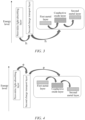
- the perovskite solar cell obtained by the steps above was marked as cell 1#, and the schematic diagram of the energy levels of the perovskite light-absorbing layer, the second charge transport layer, the first metal layer, the conductive oxide layer and the second metal layer in the cell 1# were shown in Fig. 3 .
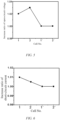
- the photoelectrical performance results of the cell 1# were shown in Table 1, and the transparency data thereof were as shown in Table 2.
- ITO indium tin oxide
- An ITO (indium tin oxide) conductive glass with a size of 2.0 cm ⁇ 2.0 cm was used, with no limitation on the thickness thereof.
- the ITO layers with a width of 0.35 cm on both opposite sides of a ITO-layer-coated glass were removed by means of a laser etching method, exposing the glass substrate.
- the etched ITO conductive glass was ultrasonically washed with water, acetone and isopropanol in order, which was repeated at least twice.
- the residual solvent on the surface of the ITO conductive glass was blow-dried with a nitrogen spray gun, and then the ITO conductive glass was placed into an ultraviolet ozone machine for further washing. The washing was carried out for 5-30 min, with no specific limitation.
- aqueous SnO 2 (tin dioxide) solution alfa
- alfa a 15% hydrocolloid dispersion solution
- the ITO conductive glass substrate that had been treated in the ultraviolet ozone machine was spin-coated with the above diluted aqueous SnO 2 solution at a rotation speed of 4,000 rpm/s with acceleration of 2,000 rpm/s 2 , and then heated at 150°C for 15 min.
- the SnO 2 layer was an electron transport layer.
- the electron transport layer prepared above was spin-coated with a perovskite precursor solution at a rate of 1,000-4,000 rpm/s, followed by annealing at 100°C for 30 min and cooling to room temperature.
- the active matter of the perovskite absorbing layer was CsFAMA, with the specific composition being Cs 0.05 (FA 0.85 MA 0.15 ) 0.95 PbI 0.93 Br 0.07 , and the concentration thereof was 1.4 mol/L;
- the solvent was a mixture of DMF (dimethylformamide) and DMSO (dimethyl sulfoxide) in a volume ratio of 4 : 1; and the CsFAMA layer was the perovskite layer.
- the perovskite layer prepared above was spin-coated with a hole transport layer of Spiro-OMeTAD (2,2',7,7'-tetra[N,N-di(4-methoxyphenyl)amino]-9,9'-spirodifluorene) at a rate of 3,000 rpm/s, with the solvent being chlorobenzene, and the concentration in mass/volume percent being 72.3 mg/mL, that is 72.3 mg of the solute was dissolved per milliliter of the solvent.
- the hole transport layer had a work function of -5.15 eV.
- the sheet prepared above was placed into an evaporation machine.
- a metal electrode of Au with a work function of -5.1 eV
- a thickness of 2 nm was evaporated at a rate of 0.1 A/s at an evaporation temperature of 30-50°C.
- cooling was performed until reaching room temperature.
- a tin-doped indium oxide, a transparent conductive oxide was sputtered by means of a radio-frequency magnetron sputtering method to form a conductive oxide thin film with a thickness of 100 nm.
- the tin-doped indium oxide had a work function of -4.85 eV.
- the tin-doped indium oxide transparent conductive oxide film was plated with a metal electrode of Ag (with a work function of -4.6 eV) with a thickness of 5 nm at a rate of 0.2 A/s by means of evaporation or sputtering, so as to form a complete composite thin-film electrode.
- the perovskite solar cell obtained by the steps above was marked as cell 2#, and the schematic diagram of the energy levels of the perovskite light-absorbing layer, the second charge transport layer, the first metal layer, the conductive oxide layer and the second metal layer in the cell 2# were shown in Fig. 4 .
- the photoelectrical performance results of the cell 2# were shown in Table 1, and the transparency data thereof were as shown in Table 2.
- the preparation process was the same as that in example 2, where the first metal layer was a cobalt layer (with a work function of -5.0 eV) with a thickness of 2 nm, the conductive oxide layer was a tin-doped indium oxide layer (with a work function of -4.85 eV) with a thickness of 100 nm, and the second metal layer was a nickel layer (with a work function of -4.6 eV) with a thickness of 5 nm.
- the photoelectrical performance results of the cell obtained in this example were as shown in Table 1, and the transparency data were as shown in Table 2.
- the preparation process was the same as that in example 2.
- the materials of the metal layers and the thickness data of the layers were as shown in Table 3.
- the photoelectrical performance results of the obtained cell were as shown in Table 1, and the transparency data were as shown in Table 2.
- the preparation process was the same as that in example 1, with the only exception that when the electrode part was finally prepared, first, a 10 nm thick molybdenum oxide was thermally evaporated, which served as a buffer layer in the magnetron sputtering process, and then a 107 nm tin-doped indium oxide layer was directly sputtered, with the work function of the tin-doped indium oxide being -4.85 eV.
- the obtained perovskite solar cell was marked as cell 1'#.
- the transparency data of the cell 1'# was as shown in Table 3, and the photoelectrical performances thereof were all normalized.
- the preparation process was the same as that in example 2, with the only exception that when the electrode part was finally prepared, first, a 10 nm thick molybdenum oxide was thermally evaporated, which served as a buffer layer in the magnetron sputtering process, and then a 107 nm thick tin-doped indium oxide layer was directly sputtered, with the work function of the tin-doped indium oxide being -4.85 eV.
- the obtained perovskite solar cell was marked as cell 2'#.
- the transparency data of the cell 2'# was as shown in Table 3, and the photoelectrical performances thereof were all normalized.
- the preparation processes were the same as those in examples 3-7, with the only exception that when the electrode part was finally prepared, first, a 10 nm thick molybdenum oxide was thermally evaporated, which served as a buffer layer in the magnetron sputtering process, and then a tin-doped indium oxide layer was directly sputtered, with the work function of the tin-doped indium oxide being -4.85 eV; and the thickness of the conductive oxide layers was the same as the total thickness of the "metal layer-conductive oxide layer-metal layer" in examples 3-7 respectively.
- the transparency data of the obtained perovskite solar cells were as shown in Table 2, and the photoelectrical performances thereof were all normalized.
- Example 1 Increase ratio of open-circuit voltage Increase ratio of short-circuit current Increase ratio of fill factor Increase ratio of light conversion efficiency
- Example 1 2.0% 1.0% 5.0% 8.0%
- Example 2 3.0% 0.6% 7.0% 10.0%
- Example 3 2.2% 0.3% 3.0% 5.0%
- Example 4 0.5% 0.9% 3.0% 4.1%
- Example 5 0.1% 0.3% 1.3% 2.1%
- Example 6 0.7% 0.6% 2.0% 3.2%
- Example 7 1.2% 1.4% 5.0% 7.1%
- Table 2 Transmittance Transmittance Example 1 58.3% Comparative example 1 57.1% Example 2 56.1% Comparative example 2 54.3% Example 3 55.7% Comparative example 3 54.3%
- Example 6 55.4% Comparative example 6 51.9%
- Material of first metal layer Thickness of first metal layer Thickness of conductive oxide layer
- Material of second metal layer Thickness of second metal layer
- test results of the above examples 1-7 and comparative examples 1-7 demonstrate that the performances of the semi-transparent perovskite solar cells based on the "metal-conductive oxide-metal" composite electrode are significantly better than those of the cells based on a blank conductive oxide.
- such semi-transparent perovskite solar cells have a better transmittance, and can maintain an unaffected semitransparent effect; and on the other hand, the photoelectrical performances thereof are improved comprehensively.
- the first metal layer that is the presence of the first metal electrode increases the transport rate of charge carriers between the charge transport layer and the thin-film composite electrode; and the second metal electrode provided on the other side of the conductive oxide layer reduces the overall series resistance of the element and facilitates the increase of the open-circuit voltage and fill factor of the element in a comprehensive manner, thereby improving the efficiency of the cell.
Landscapes
- Physics & Mathematics (AREA)
- Electromagnetism (AREA)
- Engineering & Computer Science (AREA)
- Chemical & Material Sciences (AREA)
- Materials Engineering (AREA)
- Manufacturing & Machinery (AREA)
- Inorganic Chemistry (AREA)
- Photovoltaic Devices (AREA)
Abstract
Description
- The present application claims priority to
Chinese Patent Application No. 202210113364.5, entitled "PEROVSKITE SOLAR CELL, THIN-FILM COMPOSITE ELECTRODE AND PREPARATION METHOD, POWER GENERATION APPARATUS, AND ELECTRIC APPARATUS" and filed on January 30, 2022 - The present invention relates to the technical field of batteries, and in particular to a perovskite solar cell, a thin-film composite electrode and a preparation method, a power generation apparatus, and electric apparatus.
- Perovskite solar cells have attracted widespread attention due to their better performance. Perovskite solar cells in the prior art generally comprise a charge transport layer and a thin-layer electrode adjacent thereto, which is made from a transparent conductive oxide. Since the preparation process of the transparent conductive oxide electrode requires a relatively large amount of energy, which will cause damage to the charge transport layer adjacent thereto, a buffer layer made from molybdenum oxide and other materials is provided between the transparent conductive oxide layer and the charge transport layer. However, the interposing of the buffer layer will reduce the photoelectric conversion efficiency of cells and affect the transparency of the cells.
- In view of the above problems, the present application provides a perovskite solar cell, a thin-film composite electrode and a preparation method therefor, a power generating device and a power consuming device, and can provide a semi-transparent thin-film composite electrode, which enables a perovskite solar cell cell comprising same to have excellent photoelectric performance while ensuring the transparency thereof, thus being more suitable for practical use.
- In a first aspect, the present application provides a perovskite solar cell sequentially comprising transparent conductive glass, a first charge transport layer, a perovskite absorbing layer, a second charge transport layer and a thin-film composite electrode, wherein the first charge transport layer is an electron transport layer, and the second charge transport layer is a hole transport layer; alternatively, the first charge transport layer is a hole transport layer, and the second charge transport layer is an electron transport layer; and the thin-film composite electrode comprises: a first metal layer provided on the second charge transport layer; a conductive oxide layer provided on the first metal layer; and a second metal layer provided on the conductive oxide layer.
- In the technical solution of an embodiment of the present application, the structural design of the perovskite solar cell can realize a semi-transparent (with a transmittance ≥ 50%) perovskite solar element with a first metal layer-conductive oxide layer-second metal layer as a composite electrode. Here, the thin-film composite electrode is provided with a first metal layer on the side in contact with the second charge transport layer, which can further increase the extraction rate of charge carriers at the interface, such that the probability of charge carrier recombination at the interface declines and the non-radiative recombination is reduced, thereby increasing the open-circuit voltage of the element; and a second metal layer is provided on the other side of the conductive oxide layer, which can reduce the overall series resistance of the element, increase the fill factor and finally improve the efficiency of the element.
- In some embodiments, the metal of the first metal layer is selected from at least one of gold, silver, copper, aluminum and cobalt, and alloys thereof; and the metal of the second metal layer is selected from at least one of gold, silver, copper, aluminum, nickel, zinc, tin and iron, and alloys thereof. With the material of the first metal layer and the second metal layer being defined, a better energy-level matching of materials can be achieved in the perovskite solar cell, such that the perovskite solar cell can exhibit good conductivity.
- In some embodiments, the first charge transport layer is an electron transport layer, and the second charge transport layer is a hole transport layer; and the layers in the perovskite solar cell have an HOMO energy level following an order of the perovskite absorbing layer < the second charge transport layer < the first metal layer < the conductive oxide layer < the second metal layer. The perovskite solar cell has a regular element structure, in which the three electrodes, i.e., the first metal layer, the conductive oxide layer and the second metal layer, all have a work function higher than the HOMO energy level of the second charge transport layer. In other words, the work functions of the first metal electrode, the conductive oxide electrode, and the second metal electrode are in a gradually ascending trend, which can ensure the effective transport of charge carriers between the three electrodes. With the above-mentioned technical solution, the photo-excited holes in the perovskite layer in the perovskite solar cell can be successfully conducted to the electrode end.
- In some embodiments, the first metal layer has a work function of -5.15 to -4.2 eV; the conductive oxide layer has a work function of -5.10 to -4.1 eV; the second metal layer has a work function of -4.95 to -3.5 eV; and the work function values of the second charge transport layer, the first metal layer, the conductive oxide and the second metal layer are in an ascending order; and the absolute value of the difference between the work function values of two adjacent layers is 0.02 eV - 0.3 eV. The ranges of the work function of the layers in the thin-film composite electrode are further limited to facilitate the precise selection of the material of the layers in the thin-film electrode, and meanwhile the ranges of the difference between the work function values of the layers are controlled to ensure the successful extraction and transport of photo-generated charge carriers, making it possible to better realize the successful conduction of the photo-excited holes in the perovskite layer to the electrode end.
- In some embodiments, the first charge transport layer is a hole transport layer, and the second charge transport layer is an electron transport layer; and the layers in the perovskite solar cell have a LUMO energy level following an order of the perovskite absorbing layer > the second charge transport layer > the first metal layer > the conductive oxide layer > the second metal layer. The perovskite solar cell has an inverted element structure, in which the three electrodes, i.e., the first metal layer, the conductive oxide layer and the second metal layer, all have a work function less than the LUMO energy level of the second charge transport layer. In other words, the work functions of the first metal electrode, the conductive oxide electrode, and the second metal electrode are in a gradually descending trend, which can ensure the effective transport of charge carriers between the three electrodes. With the above-mentioned technical solution, the photo-excited electrons in the perovskite layer in the perovskite solar cell can be successfully conducted to the electrode end.
- In some embodiments, the first metal layer has a work function of -4.95 to -3.5 eV; the conductive oxide layer has a work function of -5.00 to -3.65 eV; the second metal layer has a work function of -5.30 to -3.75 eV; and the work function values of the second charge transport layer, the first metal layer, the conductive oxide and the second metal layer are in a descending order; and the absolute value of the difference between the work function values of two adjacent layers is 0.02 eV - 0.3 eV. The ranges of the work function of the layers in the thin-film composite electrode are further limited to facilitate the precise selection of the material of the layers in the thin-film electrode, and meanwhile the ranges of the difference between the work function values of the layers are controlled to ensure the successful extraction and transport of photo-generated charge carriers, making it possible to better realize the successful conduction of the photo-excited electrons in the perovskite layer to the electrode end.
- In some embodiments, the conductive oxide layer has a thickness of 50-200 nm; both the first metal layer and the second metal layer have a thickness of 1-10 nm; and the sum of the thickness of the first metal layer and the second metal layer does not exceed 1/10 of the thickness of the conductive oxide layer. The technical solution of controlling the lower limits of the thickness of the layers in the thin-film composite electrode enables the thin-film composite electrode to perform the photoelectric performance thereof; and by controlling the upper limits of the thickness of the layers in the thin-film composite electrode and strictly defining that the sum of the total thickness of the first metal layer and the second metal layer does not exceed 1/10 of the thickness of the conductive oxide layer, it can ensure that the whole thin-film composite electrode is not too thick and the metal layer is relatively thin, thereby avoiding affecting the transparency of the thin-film composite electrode.
- In a second aspect, the present application provides a thin-film composite electrode provided on a charge transport layer, and the thin-film composite electrode comprises: a first metal layer provided on the charge transport layer; a conductive oxide layer provided on the first metal layer; and a second metal layer provided on the conductive oxide layer.
- In the technical solutions of an embodiment of the present application, the structural design of the thin-film composite electrode can realize a semi-transparent (with a transmittance ≥ 50%) solar cell element without increasing the contact resistance and evaporation temperature of the electrode. The thin-film composite electrode is provided with a first metal layer on the side in contact with the charge transport layer, which can further increase the extraction rate of charge carriers at the interface, such that the probability of charge carrier recombination at the interface declines and the non-radiative recombination is reduced, thereby increasing the open-circuit voltage of the element; and a second metal layer is provided on the other side of the conductive oxide layer, which can reduce the overall series resistance of the element, increase the fill factor and finally improve the efficiency of the element.
- In some embodiments, the conductive oxide layer has a thickness of 50-200 nm; both the first metal layer and the second metal layer have a thickness of 1-10 nm; and the sum of the thickness of the first metal layer and the second metal layer does not exceed 1/10 of the thickness of the conductive oxide layer. The thickness of the metal electrode will affect the overall transmittance of the element. When the total thickness of the metal electrodes is too large, the transmittance of the element will be greatly reduced, making it unable to meet the application requirements for semi-transparent elements. Further, the metal layers in the thin-film composite electrode are controlled to be thin, and specifically, when the ratio of the total thickness of the metal electrodes to the thickness of the conductive transparent electrode is < 1/10, the element appears to be semi-transparent, and the photoelectric conversion efficiency of the thin-film composite electrode will be improved to a certain extent. The technical solution of controlling the lower limits of the thickness of the layers in the thin-film composite electrode enables the thin-film composite electrode to perform the photoelectric performance thereof; and by controlling the upper limits of the thickness of the layers in the thin-film composite electrode and strictly defining that the sum of the total thickness of the first metal layer and the second metal layer does not exceed 1/10 of the thickness of the conductive oxide layer, it can ensure that the whole thin-film composite electrode is not too thick and the metal layer is relatively thin, thereby avoiding affecting the transparency of the thin-film composite electrode.
- In some embodiments, the conductive oxide layer has a thickness of 100-150 nm. By further defining the thickness of the conductive oxide layer, it can achieve a better balance between the photoelectric performance and transparency of the thin-film composite electrode, and the thin-film composite electrode will have a conductivity at a better level on the basis of ensuring that the thin-film composite electrode is semi-transparent.
- In a third aspect, the present application provides a preparation method of the aforementioned thin-film composite electrode, wherein the thin-film composite electrode is provided on a charge transport layer; and the preparation method comprises the steps of:
- 1) providing the charge transport layer with a first metal layer;
- 2) providing the first metal layer with a conductive oxide layer; and
- 3) providing the conductive oxide with a second metal layer.
- In the technical solution of an embodiment of the present application, a first metal layer, a conductive oxide layer and a second metal layer are sequentially provided on the charge transport layer to obtain a transparent composite electrode with a structure of metal layer-transparent conductive oxide layer-metal layer.
- In some embodiments, the first metal layer is prepared by means of evaporation with a vacuum degree ≤ 5 × 10⁻⁴ Pa, at a temperature ≤ 100°C and a rate ≤ 0.1 A/s; the conductive oxide layer is prepared by means of vacuum sputtering or vacuum evaporation with a vacuum degree ≤ 5 × 10⁻⁴ Pa at a rate of 0.1 A/s to 1 A/s; the second metal layer is prepared by means of vacuum sputtering or vacuum evaporation with a vacuum degree ≤ 5 × 10⁻⁴ Pa at a rate of 0. 1-0.5 A/s; and the preparation method further comprises the steps of: with the vacuum degree being maintained, cooling to room temperature between step 1) and step 2); and carrying out step 2) and step 3) continuously with the vacuum degree being maintained. With the strict definition of the preparation processes of the first metal layer, the conductive oxide layer and the second metal layer, and the strict definitions that the vacuum cannot be broken and the evaporation should be stopped for a period of time between the preparation of the conductive oxide layer and the preparation of the first metal layer and the vacuum cannot be broken between the preparation of the second metal layer and preparation of the conductive oxide layer, a metal-conductive oxide-metal composite electrode required by the technical solution of the present invention is obtained, which appears to be semitransparent and is not prone to delamination.
- In a fourth aspect, the present application provides a power generating device comprising the perovskite solar cell in the above-mentioned embodiment.
- In a fifth aspect, the present application provides a power consuming device comprising the aforementioned perovskite solar cell, with the perovskite solar cell being used to supply electrical energy.
- The above description is only an overview of the technical solutions of the present application. To more clearly understand the technical means of the present application to implement same according to the contents of the description, and to make the above and other objectives, features, and advantages of the present application more obvious and understandable, specific implementations of the present application are exemplarily described below.
- Various other advantages and benefits will become obvious to those of ordinary skill in the art upon reading the following detailed description of preferred implementations. The accompanying drawings are merely for the purpose of illustrating the preferred implementations, and should not be construed as limiting the present application. Moreover, like components are denoted by like reference signs throughout the accompanying drawings. In the drawings:
-
Fig. 1 shows a schematic diagram of the structure of a perovskite solar cell according to some embodiments of the present application; -
Fig. 2 shows a schematic diagram of a thin-film composite electrode according to some embodiments of the present application; -
Fig. 3 shows a schematic diagram of the energy level of a regular perovskite solar cell element according to some embodiments of the present application; -
Fig. 4 shows a schematic diagram of the energy level of an inverted perovskite solar cell element according to some embodiments of the present application; -
Fig. 5 shows a performance graph of the open-circuit voltage of a perovskite solar cell according to some embodiments of the present application; -
Fig. 6 shows a performance graph of the short-circuit current of a perovskite solar according to some embodiments of the present application; -
Fig. 7 shows a performance graph of the fill factor of a perovskite solar according to some embodiments of the present application; -
Fig. 8 shows a performance graph of the photoelectric conversion efficiency of a perovskite solar according to some embodiments of the present application. - Reference signs in the Detailed Description of Embodiments:
thin-film composite electrode 1; secondcharge transport layer 2,perovskite absorbing layer 3, firstcharge transport layer 4, transparentconductive glass 5;first metal layer 11,conductive oxide layer 12,second metal layer 13. - Embodiments of the technical solutions of the present application will be described in detail below with reference to the accompanying drawings. The following embodiments are merely intended to more clearly illustrate the technical solutions of the present application, so they merely serve as examples, but are not intended to limit the scope of protection of the present application.
- Unless otherwise defined, all technical and scientific terms used herein have the same meanings as those commonly understood by those skilled in the art to which the present application belongs. The terms used herein are merely for the purpose of describing specific embodiments, but are not intended to limit the present application. The terms "include/comprise" and "has/have" and any variations thereof in the description and the claims of the present application as well as the brief description of the accompanying drawings described above are intended to cover non-exclusive inclusion.
- In the description of the embodiments of the present application, the technical terms "first", "second", etc. are merely used for distinguishing different objects, and are not to be construed as indicating or implying relative importance or implicitly indicating the number, particular order or primary-secondary relationship of the indicated technical features. In the description of the embodiments of the present application, the phrase "multiple" means two or more, unless otherwise explicitly and specifically defined.
- The phrase "embodiment" mentioned herein means that the specific features, structures, or characteristics described in conjunction with the embodiment can be encompassed in at least one embodiment of the present application. The phrase at various locations in the description does not necessarily refer to the same embodiment, or an independent or alternative embodiment exclusive of another embodiment. Those skilled in the art understand explicitly or implicitly that the embodiment described herein may be combined with another embodiment.
- In the description of the embodiments of the present application, the term "and/or" is merely intended to describe the associated relationship of associated objects, indicating that three relationships can exist. For example, A and/or B can include: only A exists, both A and B exist, and only B exists. In addition, the character "/" herein generally indicates an "or" relationship between the associated objects.
- In the description of the embodiments of the present application, the term "multiple" means two or more (including two), similarly the term "multiple groups" means two or more groups (including two groups), and the term "multiple pieces" means two or more pieces (including two pieces).
- In the description of the embodiments of the present application, the orientations or positional relationships indicated by the technical terms "central", "longitudinal", "transverse", "length", "width", "thickness", "upper", "lower", "front", "rear", "left", "right", "vertical", "horizontal", "top", "bottom", "inner", "outer", "clockwise", "counterclockwise", "axial", "radial", "circumferential", etc. are based on the orientations or positional relationships shown in the accompanying drawings, are merely intended to facilitate and simplify the description of the embodiments of the present application, rather than indicating or implying that the apparatus or element referred to must have a particular orientation or be constructed and operated in a particular orientation, and therefore cannot be construed as limiting the embodiments of the present application.
- In the description of the embodiments of the present application, unless otherwise explicitly specified and defined, the technical terms such as "mount", "couple", "connect", and "fix" should be understood in a broad sense. For example, they may be a fixed connection, a detachable connection, or an integrated connection; may be a mechanical connection or an electric connection; and may be a direct connection or an indirect connection by means of an intermediate medium, or may be communication between interiors of two elements or interaction between the two elements. For those of ordinary skill in the art, the specific meanings of the above terms in the embodiments of the present application can be understood according to specific situations.
- In the prior art, perovskite solar cells have attracted widespread attentions due to their better performance. However, the perovskite solar cells in the prior art generally comprise a charge transport layer and a thin-layer electrode adjacent thereto, which is made from a transparent conductive oxide. Since the preparation process of the transparent conductive oxide electrode requires a relatively large amount of energy, which will cause damage to the charge transport layer adj acent thereto, a buffer layer made from molybdenum oxide and other materials needs to be provided between the transparent conductive oxide layer and the charge transport layer.
- The inventors noticed that providing a buffer layer between the charge transport layer and the electrode layer may result in the decrease of the photoelectric conversion efficiency of cells and affect the transparency of the cells.
- In order to solve the above-mentioned problems, the applicant has found through research that a semi-transparent thin-film composite electrode can be obtained by providing a first metal layer on the surface of a charge transport layer, then providing a conductive oxide layer on the first metal layer, and finally providing a second metal layer on the conductive oxide layer, which enables the semi-transparent thin-film composite electrode to have a relatively high photoelectric conversion efficiency while ensuring the transparency thereof.
- The thin-film composite electrode disclosed in an embodiment of the present application can be applied to a perovskite solar cell sequentially comprising transparent conductive glass, a first charge transport layer, a perovskite absorbing layer, a second charge transport layer and a thin-film composite electrode; wherein the first charge transport layer is an electron transport layer, and the second charge transport layer is a hole transport layer; alternatively, the first charge transport layer is a hole transport layer, and the second charge transport layer is an electron transport layer; and the thin-film composite electrode comprises: a first metal layer provided on the second charge transport layer; a conductive oxide layer provided on the first metal layer; and a second metal layer provided on the conductive oxide layer. With the above-mentioned technical solution, a semi-transparent perovskite solar element with a first metal layer-conductive oxide layer-second metal layer as a composite electrode can be obtained, which has not only a certain degree of transparency but also good photoelectric conversion efficiency.
- When preparing the thin-film composite electrode disclosed in an embodiment of the present application, the thin-film composite electrode is provided on a charge transport layer; and the preparation method comprises the steps of: 1) providing the charge transport layer with a first metal layer; 2) providing the first metal layer with a conductive oxide layer; and 3) providing the conductive oxide with a second metal layer. With the above-mentioned technical solution, a transparent composite electrode with a structure of metal layer-transparent conductive oxide layer-metal layer can be obtained. The thin-film composite electrode can have a relatively high photoelectric conversion efficiency while ensuring the transparency thereof.
- The perovskite solar cells disclosed in an embodiment of the present application can be applied in a power generating device, which can ensure the transparency of the power generating device and also enable same to have a relatively high photoelectric conversion efficiency, thus being applicable to application situations requiring both transparency and conductivity.
- The perovskite solar cell disclosed in an embodiment of the present application can be applied in the cell of a power consuming device. The power consuming device comprises the aforementioned perovskite solar cell, which is used to supply electrical energy and can be used in application situations requiring both transparency and conductivity.
- For the convenience of explanation, the following embodiments will be described with a thin-film composite electrode and a perovskite solar cell of an embodiment of the present application as examples.
- Reference can be made to
Fig. 1 , which shows a schematic diagram of a perovskite solar cell according to some embodiments of the present application. As shown inFig. 1 , the perovskite solar cell has a layered structure and comprises transparentconductive glass 5, a firstcharge transport layer 4, aperovskite absorbing layer 3, a secondcharge transport layer 2 and a thin-film composite electrode 1 that are provided sequentially; wherein the firstcharge transport layer 4 is an electron transport layer, and the secondcharge transport layer 2 is a hole transport layer; alternatively, the firstcharge transport layer 4 is a hole transport layer, and the secondcharge transport layer 2 is an electron transport layer; and the thin-film composite electrode 1 comprises: afirst metal layer 11 provided on the secondcharge transport layer 2; aconductive oxide layer 12 provided on thefirst metal layer 11; and asecond metal layer 13 provided on theconductive oxide layer 12. - Reference can be made to
Fig. 2 , which is a schematic diagram of the structure of a thin-film composite electrode provided in some embodiments of the present application. As shown inFig. 2 , the thin-film composite electrode has a three-layer structure, in which a conductive oxide layer is sandwiched between metal layers, forming a thin-film composite electrode composed of three layers of films of metal layer-conductive oxide layer-metal layer. When the thin-film composite electrode is used, one of the metal layers is provided on a charge transport layer. - According to some embodiments of the present application, the present application provides a thin-film composite electrode provided on a charge transport layer. The thin-film composite electrode comprises: a first metal layer provided on the charge transport layer; a conductive oxide layer provided on the first metal layer; and a second metal layer provided on the conductive oxide layer.
- The structural design of the thin-film composite electrode can realize a semitransparent solar cell element without increasing the contact resistance and evaporation temperature of the electrode. The thin-film composite electrode is provided with a first metal layer on the side in contact with the charge transport layer, which can further increase the extraction rate of charge carriers at the interface, such that the probability of charge carrier recombination at the interface declines and the non-radiative recombination is reduced, thereby increasing the open-circuit voltage of the element; and a second metal layer is provided on the other side of the conductive oxide layer, which can reduce the overall series resistance of the element, increase the fill factor and finally improve the efficiency of the element.
- According to some embodiments of the present application, it is preferred that the thin-film composite electrode is directly provided on a charge transport layer, the thin-film composite electrode comprising: a first metal layer directly provided on the charge transport layer; a conductive oxide layer directly provided on the first metal layer; and a second metal layer directly provided on the conductive oxide layer.
- According to some embodiments of the present application, it is preferred that modification layers are provided between the charge transport layer, the first metal layer, the conductive oxide layer and the second metal layer.
- According to some embodiments of the present application, the metal of the first metal layer is selected from at least one of gold, silver, copper, aluminum and cobalt, and alloys thereof; the material of the conductive oxide layer is at least one of tin-doped indium oxide, tungsten-doped indium oxide, fluorine-doped tin oxide, aluminum-doped zinc oxide, indium zinc oxide and zinc tin oxide; and the metal of the second metal layer is selected from at least one of gold, silver, copper, aluminum, nickel, zinc, tin and iron, and alloys thereof.
- According to some embodiments of the present application, it is preferred that the conductive oxide layer has a thickness of 50-200 nm; both the first metal layer and the second metal layer have a thickness of 1-10 nm; and the sum of the thickness of the first metal layer and the second metal layer does not exceed 1/10 of the thickness of the conductive oxide layer. The thickness of the metal electrode will affect the overall transmittance of the element. When the total thickness of the metal electrodes is too large, the transmittance of the element will be greatly reduced, making it unable to meet the application requirements for semi-transparent elements. Further, the metal layers in the thin-film composite electrode are controlled to be thin, and specifically, when the ratio of the total thickness of the metal electrodes to the thickness of the conductive transparent electrode is < 1/10, the element appears to be semi-transparent, and the photoelectric conversion efficiency of the thin-film composite electrode will be improved to a certain extent. The technical solution of controlling the lower limits of the thickness of the layers in the thin-film composite electrode enables the thin-film composite electrode to perform the photoelectric performance thereof; and by controlling the upper limits of the thickness of the layers in the thin-film composite electrode and strictly defining that the sum of the total thickness of the first metal layer and the second metal layer does not exceed 1/10 of the thickness of the conductive oxide layer, it can ensure that the whole thin-film composite electrode is not too thick and the metal layer is relatively thin, thereby avoiding affecting the transparency of the thin-film composite electrode.
- According to some embodiments of the present application, it is preferred that the conductive oxide layer has a thickness of 100-150 nm. By further defining the thickness of the conductive oxide layer, it can achieve a better balance between the photoelectric performance and transparency of the thin-film composite electrode, and the thin-film composite electrode will have a conductivity at a better level on the basis of ensuring that the thin-film composite electrode is semi-transparent.
- According to some embodiments of the present application, the present application provides a perovskite solar cell sequentially comprising transparent conductive glass, a first charge transport layer, a perovskite absorbing layer, a second charge transport layer and a thin-film composite electrode; wherein the first charge transport layer is an electron transport layer, and the second charge transport layer is a hole transport layer; alternatively, the first charge transport layer is a hole transport layer, and the second charge transport layer is an electron transport layer; and the thin-film composite electrode comprises: a first metal layer provided on the second charge transport layer; a conductive oxide layer provided on the first metal layer; and a second metal layer provided on the conductive oxide layer.
- The structural design of the perovskite solar cell can realize a semi-transparent perovskite solar element with a first metal layer-conductive oxide layer-second metal layer as a composite electrode.
- According to some embodiments of the present application, it is preferred that the first metal layer is directly provided on the second charge transport layer, the conductive oxide layer is directly provided on the first metal layer, and the second metal layer is directly provided on the conductive oxide layer.
- According to some embodiments of the present application, it is preferred that corresponding modification layers can be interposed between every two layers of the transparent conductive glass, the first charge transport layer, the perovskite absorbing layer, the second charge transport layer, and the thin-film composite electrode layer, so as to improve the performance of the perovskite solar cell. The transparent conductive glass is the light incident surface of the perovskite solar cell.
- According to some embodiments of the present application, it is preferred that the metal of the first metal layer is selected from at least one of gold, silver, copper, aluminum and cobalt, and alloys thereof; the metal of the second metal layer is selected from at least one of gold, silver, copper, aluminum, nickel, zinc, tin and iron, and alloys thereof. With the material of the first metal layer and the second metal layer being defined, a better energy-level matching of materials can be achieved in the perovskite solar cell, such that the perovskite solar cell can exhibit good conductivity.
- According to some embodiments of the present application, it is preferred that the first charge transport layer is an electron transport layer, and the second charge transport layer is a hole transport layer; and the layers in the perovskite solar cell have an HOMO energy level following an order of the perovskite absorbing layer < the second charge transport layer < the first metal layer < the conductive oxide layer < the second metal layer. The perovskite solar cell has a regular element structure, in which the three electrodes, i.e., the first metal layer, the conductive oxide layer and the second metal layer, all have a work function higher than the HOMO energy level of the second charge transport layer. In other words, the work functions of the first metal electrode, the conductive oxide electrode, and the second metal electrode are in a gradually ascending trend, which can ensure the effective transport of charge carriers between the three electrodes. With the above-mentioned technical solution, the photo-excited holes in the perovskite layer in the perovskite solar cell can be successfully conducted to the electrode end.
- According to some embodiments of the present application, it is preferred that the first metal layer has a work function of -5.15 to -4.2 eV; the conductive oxide layer has a work function of -5.10 to -4.1 eV; the second metal layer has a work function of -4.95 to - 3.5 eV; and the work function values of the second charge transport layer, the first metal layer, the conductive oxide and the second metal layer are in an ascending order; and the absolute value of the difference between the work function values of two adjacent layers is 0.02 eV - 0.3 eV. The ranges of the work function of the layers in the thin-film composite electrode are further limited to facilitate the precise selection of the material of the layers in the thin-film electrode, and meanwhile the ranges of the difference between the work function values of the layers are controlled to ensure the successful extraction and transport of photo-generated charge carriers, making it possible to better realize the successful conduction of the photo-excited holes in the perovskite layer to the electrode end.
- According to some embodiments of the present application, it is preferred that the first charge transport layer is a hole transport layer, and the second charge transport layer is an electron transport layer; and the layers in the perovskite solar cell have a LUMO energy level following an order of the perovskite absorbing layer > the second charge transport layer > the first metal layer > the conductive oxide layer > the second metal layer. The perovskite solar cell has an inverted element structure, in which the three electrodes, i.e., the first metal layer, the conductive oxide layer and the second metal layer, all have a work function less than the LUMO energy level of the second charge transport layer. In other words, the work functions of the first metal electrode, the conductive oxide electrode, and the second metal electrode are in a gradually descending trend, which can ensure the effective transport of charge carriers between the three electrodes. With the above-mentioned technical solution, the photo-excited electrons in the perovskite layer in the perovskite solar cell can be successfully conducted to the electrode end.
- According to some embodiments of the present application, it is preferred that the first metal layer has a work function of -4.95 to -3.5 eV; the conductive oxide layer has a work function of -5.00 to -3.65 eV; the second metal layer has a work function of -5.30 to - 3.75 eV; and the work function values of the second charge transport layer, the first metal layer, the conductive oxide and the second metal layer are in a descending order; and the absolute value of the difference between the work function values of two adjacent layers is 0.02 eV - 0.3 eV. The ranges of the work function of the layers in the thin-film composite electrode are further limited to facilitate the precise selection of the material of the layers in the thin-film electrode, and meanwhile the ranges of the difference between the work function values of the layers are controlled to ensure the successful extraction and transport of photo-generated charge carriers, making it possible to better realize the successful conduction of the photo-excited electrons in the perovskite layer to the electrode end.
- The term HOMO mentioned above is the abbreviation of Highest Occupied Molecular Orbital. The term LUMO mentioned above is the abbreviation of Lowest Unoccupied Molecular Orbital. The energy difference between the HOMO and LUMO is called "energy band gap", that is the so-called HOMO-LUMO energy level, which can sometimes be used to measure whether a molecule will be easily excited. A smaller band gap indicates an easier molecule excitation. The HOMO in organic semiconductors and quantum dots is similar to the valence band in inorganic semiconductors, while the LUMO is similar to the conduction band. The HOMO energy level refers to the valence band maximum (VBM). The LUMO energy level refers to the conduction band minimum (CBM).
- For semiconductors, the work function refers to the minimum energy required for an electron to immediately escape from a solid, which is an inherent characteristic and intrinsic feature of a material itself. In the thin-film composite electrode, it is necessary to maintain a difference between the energy levels of two adjacent layers. When the absolute value of the energy level difference is less than 0.02 eV, the built-in electrical field of the electrode cannot be formed, making it impossible for charges to transfer in a certain direction; and when the absolute value of the energy level difference is greater than 0.3 eV, it will cause significant open-circuit voltage loss, which is not conducive to the improvement of element performance.
- According to some embodiments of the present application, it is preferred that the conductive oxide layer has a thickness of 50-200 nm; both the first metal layer and the second metal layer have a thickness of 1-10 nm; and the sum of the thickness of the first metal layer and the second metal layer does not exceed 1/10 of the thickness of the conductive oxide layer. The technical solution of controlling the lower limits of the thickness of the layers in the thin-film composite electrode enables the thin-film composite electrode to perform the photoelectric performance thereof; and by controlling the upper limits of the thickness of the layers in the thin-film composite electrode and strictly defining that the sum of the total thickness of the first metal layer and the second metal layer does not exceed 1/10 of the thickness of the conductive oxide layer, it can ensure that the whole thin-film composite electrode is not too thick and the metal layer is relatively thin, thereby avoiding affecting the transparency of the thin-film composite electrode.
- According to some embodiments of the present application, the perovskite solar cell is a semi-transparent cell. This is because, on the one hand, the total thickness of the perovskite solar cell is 52-220 nm, and meanwhile, it is particularly defined that the sum of the thickness of the first metal layer and the second metal layer does not exceed 1/10 of the thickness of the conductive oxide layer, that is the maximum of the sum of the thickness of the metal layers in the thin-film composite electrode of the present invention does not exceed 20 nm; therefore, the transparency of the conductive oxide layer is not greatly affected, making the perovskite solar cell have a property of being semi-transparent and be applicable in glass elements.
- According to some embodiments of the present application, the material of the transparent conductive glass is selected from at least one of fluorine-doped indium oxide, indium-doped tin oxide, aluminum-doped zinc oxide, beryllium-doped zinc oxide, and indium-doped zinc oxide.
- According to some embodiments of the present application, the chemical formula of the perovskite light-absorbing layer is ABX3 or A2CDX6, where A represents a positively monovalent inorganic cation and/or organic cation, B represents a positively divalent metal cation, C represents a positively monovalent metal cation, D represents a positively trivalent metal cation, and X is an inorganic anion and/or organic anion.
- According to some embodiments of the present application, the positively divalent metal cation is a lead ion or a tin ion.
- According to some embodiments of the present application, the perovskite light-absorbing layer has a band gap of 1.20-2.30 eV and a thickness of 200-1000 nm.
- According to some embodiments of the present application, the electron transport layer is selected from at least one of methyl [6,6]-phenyl-C61-butyrate, methyl [6,6]-phenyl-C71-butyrate, fullerene C60, fullerene C70, tin dioxide and zinc oxide, and derivatives of the above materials, or materials modified by means of doping or passivating the above materials.
- According to some embodiments of the present application, the hole transport layer is selected from at least one of 2,2',7,7'-tetra(N,N-p-methoxyphenylamino)-9,9'-spirodifluorene, poly[bis(4-phenyl)(2,4,6-trimethylphenyl)amine], methoxytriphenylaminefluoroformamidine, poly(3,4-ethylenedioxythiophene) : poly(styrenesulfonate), poly(3-hexylthiophene), cuprous thiocyanate, nickel oxide, triptycene-cored triphenylamine, 3,4-ethylenedioxythiophene-methoxytriphenylamine, N-(4-aniline)carbazole-spirobifluorene (CzPAF-SBF) and polythiophene, and derivatives of the above materials, or materials modified by means of doping or passivating the above materials.
- According to some embodiments of the present application, the material of the conductive oxide layer is at least one of tin-doped indium oxide, tungsten-doped indium oxide, fluorine-doped tin oxide, aluminum-doped zinc oxide, indium zinc oxide, and zinc tin oxide.
- According to some embodiments of the present application, the present application provides a preparation method of the aforementioned thin-film composite electrode, wherein the thin-film composite electrode is provided on a charge transport layer; and the preparation method comprises the steps of:
- 1) providing the charge transport layer with a first metal layer;
- 2) providing the first metal layer with a conductive oxide layer; and
- 3) providing the conductive oxide with a second metal layer.
- In the technical solution of an embodiment of the present application, a first metal layer, a conductive oxide layer and a second metal layer are sequentially provided on the charge transport layer to obtain a transparent composite electrode with a structure of metal layer-transparent conductive oxide layer-metal layer.
- According to some embodiments of the present application, it is preferred that the first metal layer is prepared by means of evaporation with a vacuum degree ≤ 5×10⁻⁴ Pa, at a temperature ≤ 100°C and a rate ≤ 0.1 A/s; the conductive oxide layer is prepared by means of vacuum sputtering or vacuum evaporation with a vacuum degree ≤ 5 × 10⁻⁴ Pa at a rate of 0.1 A/s to 1 A/s; the second metal layer is prepared by means of vacuum sputtering or vacuum evaporation with a vacuum degree ≤ 5 × 10⁻⁴ Pa at a rate of 0.1-0.5 A/s; and the preparation method further comprises the steps of: with the vacuum degree being maintained, cooling to room temperature between step 1) and step 2); and carrying out step 2) and step 3) continuously with the vacuum degree being maintained. With the strict definition of the preparation processes of the first metal layer, the conductive oxide layer and the second metal layer, and the strict definitions that the vacuum cannot be broken and the evaporation should be stopped for a period of time between the preparation of the conductive oxide layer and the preparation of the first metal layer and the vacuum cannot be broken between the preparation of the second metal layer and preparation of the conductive oxide layer, a metal-conductive oxide-metal composite electrode required by the technical solution of the present invention is obtained, which appears to be semi-transparent and is not prone to delamination.
- The present application will be further described below with reference to specific embodiments.
- The performance of the cells is tested under irradiation with standard simulated sunlight (AM 1.5 G, 100 mW/cm2), so as to obtain an I-V curve.
- On the basis of the I-V curve and the data from the test apparatus, the short-circuit current Jsc (in mA), open-circuit voltage Voc (in V), maximum light-generated current Jmpp (in mA) and maximum light-generated voltage Vmpp (in V) can be obtained.
- The fill factor FF (in %) of a cell is calculated according to the formula FF = Jsc × Voc/(Jmpp × Vmpp).
- The photoelectrical conversion efficiency PCE (in %) of a cell is calculated according to the formula PCE = Jsc × Voc × FF/Pw, where Pw represents input power (in mW).
- For the convenience of performance comparison, the present invention normalizes parameters such as short-circuit current, open-circuit voltage, fill factor and photoelectrical conversion efficiency with the numerical values of the comparative example corresponding to each example as a standard, which can allow the intuitive comparison of element parameters and performance improvements.
- An ITO (indium tin oxide) conductive glass with a size of 2.0 cm × 2.0 cm was used, with no limitation on the thickness thereof. The ITO layers with a width of 0.35 cm on both opposite sides of a ITO-layer-coated glass were removed by means of a laser etching method, exposing the glass substrate.
- The etched ITO conductive glass was ultrasonically washed with water, acetone and isopropanol in order, which was repeated at least twice.
- The residual solvent on the surface of the ITO conductive glass was blow-dried with a nitrogen spray gun, and then the ITO conductive glass was placed into an ultraviolet ozone machine for further washing. The washing was carried out for 5-30 min, with no specific limitation.
- A solution of PTAA (poly[bis(4-phenyl)(2,4,6-trimethylphenyl)amine]) in isopropanol was prepared, with a concentration in mass/volume percent of 2 mg/mL, that is 2 mg of the solute was dissolved per milliliter of the solvent.
- The PTAA solution prepared above was spin-coated onto the ITO conductive glass substrate that had been treated in the ultraviolet ozone machine at a rate of 5,000 rpm/s, followed by an annealing treatment for 10 min on a 100°C heating platform. The PTAA layer was an organic hole transport layer.
- A perovskite precursor solution was spin-coated onto the organic hole transport layer prepared above at a rate of 1,000-5,000 rpm/s, followed by annealing at 100°C for 30 min and cooling to room temperature. Here, the active matter of the perovskite absorbing layer was CsFAMA, with the specific composition being Cs0.05(FA0.85MA0.15)0.95PbI0.93Br0.07, and the concentration thereof was 1.4 mol/L; the solvent was a mixture of DMF (dimethylformamide) and DMSO (dimethyl sulfoxide) in a volume ratio of 4 : 1; and the CsFAMA layer was the perovskite layer.
- PC61BM (methyl [6,6]-phenyl-C61-butyrate) was spin-coated onto the perovskite layer prepared above at a rate of 1,000-1,500 rpm/s, followed by annealing at 100°C for 10 min. Then BCP (bathocuproine) was immediately spin-coated at a rate of 5,000 rpm/s. Here, the concentration in mass/volume percent of PC61BM was 20 mg/mL, that is 20 mg of the solute was dissolved per milliliter of a solvent; the solvent was chlorobenzene; the concentration in mass/volume percent of BCP was 0.5 mg/mL, that is 0.5 mg of the solute was dissolved per milliliter of a solvent; the solvent was isopropanol; the PC61BM layer was an electron transport layer; the BCP layer was a passivation layer; and the second charge transport layer has a work function of -4.40 eV.
- The sheet prepared above was placed into an evaporation machine. When the vacuum degree of evaporation was 5 × 10⁻⁴ Pa or less, a metal electrode of Cu (with a work function of -4.65 eV) with a thickness of 2 nm was evaporated at a rate of 0.1 A/s at an evaporation temperature of 30-50°C. With the vacuum degree being maintained without break off, cooling was performed until reaching room temperature. Then, a tin-doped indium oxide, a transparent conductive oxide, was sputtered by means of a radio-frequency magnetron sputtering method to form a conductive oxide thin film with a thickness of 100 nm. The tin-doped indium oxide had a work function of -4.85 eV. Finally, with the vacuum degree being maintained without break off, the tin-doped indium oxide transparent conductive oxide film was plated with a metal electrode of Au (with a work function of -5.1 eV) with a thickness of 5 nm at a rate of 0.2 A/s by means of evaporation or sputtering, so as to form a complete composite thin-film electrode.
- The perovskite solar cell obtained by the steps above was marked as
cell 1#, and the schematic diagram of the energy levels of the perovskite light-absorbing layer, the second charge transport layer, the first metal layer, the conductive oxide layer and the second metal layer in thecell 1# were shown inFig. 3 . The photoelectrical performance results of thecell 1# were shown in Table 1, and the transparency data thereof were as shown in Table 2. - An ITO (indium tin oxide) conductive glass with a size of 2.0 cm × 2.0 cm was used, with no limitation on the thickness thereof. The ITO layers with a width of 0.35 cm on both opposite sides of a ITO-layer-coated glass were removed by means of a laser etching method, exposing the glass substrate.
- The etched ITO conductive glass was ultrasonically washed with water, acetone and isopropanol in order, which was repeated at least twice.
- The residual solvent on the surface of the ITO conductive glass was blow-dried with a nitrogen spray gun, and then the ITO conductive glass was placed into an ultraviolet ozone machine for further washing. The washing was carried out for 5-30 min, with no specific limitation.
- A commercially-available aqueous SnO2 (tin dioxide) solution (alfa), a 15% hydrocolloid dispersion solution, was purchased and diluted with 3 times distilled water for later use.
- The ITO conductive glass substrate that had been treated in the ultraviolet ozone machine was spin-coated with the above diluted aqueous SnO2 solution at a rotation speed of 4,000 rpm/s with acceleration of 2,000 rpm/s2, and then heated at 150°C for 15 min. The SnO2 layer was an electron transport layer.
- The electron transport layer prepared above was spin-coated with a perovskite precursor solution at a rate of 1,000-4,000 rpm/s, followed by annealing at 100°C for 30 min and cooling to room temperature. Here, the active matter of the perovskite absorbing layer was CsFAMA, with the specific composition being Cs0.05(FA0.85MA0.15)0.95PbI0.93Br0.07, and the concentration thereof was 1.4 mol/L; the solvent was a mixture of DMF (dimethylformamide) and DMSO (dimethyl sulfoxide) in a volume ratio of 4 : 1; and the CsFAMA layer was the perovskite layer.
- The perovskite layer prepared above was spin-coated with a hole transport layer of Spiro-OMeTAD (2,2',7,7'-tetra[N,N-di(4-methoxyphenyl)amino]-9,9'-spirodifluorene) at a rate of 3,000 rpm/s, with the solvent being chlorobenzene, and the concentration in mass/volume percent being 72.3 mg/mL, that is 72.3 mg of the solute was dissolved per milliliter of the solvent. The hole transport layer had a work function of -5.15 eV.
- The sheet prepared above was placed into an evaporation machine. When the vacuum degree of evaporation was 5 × 10⁻⁴ Pa or less, a metal electrode of Au (with a work function of -5.1 eV) with a thickness of 2 nm was evaporated at a rate of 0.1 A/s at an evaporation temperature of 30-50°C. With the vacuum degree being maintained without break off, cooling was performed until reaching room temperature. Then, a tin-doped indium oxide, a transparent conductive oxide, was sputtered by means of a radio-frequency magnetron sputtering method to form a conductive oxide thin film with a thickness of 100 nm. The tin-doped indium oxide had a work function of -4.85 eV. Finally, with the vacuum degree being maintained without break off, the tin-doped indium oxide transparent conductive oxide film was plated with a metal electrode of Ag (with a work function of -4.6 eV) with a thickness of 5 nm at a rate of 0.2 A/s by means of evaporation or sputtering, so as to form a complete composite thin-film electrode.
- The perovskite solar cell obtained by the steps above was marked as
cell 2#, and the schematic diagram of the energy levels of the perovskite light-absorbing layer, the second charge transport layer, the first metal layer, the conductive oxide layer and the second metal layer in thecell 2# were shown inFig. 4 . The photoelectrical performance results of thecell 2# were shown in Table 1, and the transparency data thereof were as shown in Table 2. - The preparation process was the same as that in example 2, where the first metal layer was a cobalt layer (with a work function of -5.0 eV) with a thickness of 2 nm, the conductive oxide layer was a tin-doped indium oxide layer (with a work function of -4.85 eV) with a thickness of 100 nm, and the second metal layer was a nickel layer (with a work function of -4.6 eV) with a thickness of 5 nm. The photoelectrical performance results of the cell obtained in this example were as shown in Table 1, and the transparency data were as shown in Table 2.
- The preparation process was the same as that in example 2. The materials of the metal layers and the thickness data of the layers were as shown in Table 3. The photoelectrical performance results of the obtained cell were as shown in Table 1, and the transparency data were as shown in Table 2.
- The preparation process was the same as that in example 1, with the only exception that when the electrode part was finally prepared, first, a 10 nm thick molybdenum oxide was thermally evaporated, which served as a buffer layer in the magnetron sputtering process, and then a 107 nm tin-doped indium oxide layer was directly sputtered, with the work function of the tin-doped indium oxide being -4.85 eV. The obtained perovskite solar cell was marked as cell 1'#. The transparency data of the cell 1'# was as shown in Table 3, and the photoelectrical performances thereof were all normalized.
- The preparation process was the same as that in example 2, with the only exception that when the electrode part was finally prepared, first, a 10 nm thick molybdenum oxide was thermally evaporated, which served as a buffer layer in the magnetron sputtering process, and then a 107 nm thick tin-doped indium oxide layer was directly sputtered, with the work function of the tin-doped indium oxide being -4.85 eV. The obtained perovskite solar cell was marked as cell 2'#. The transparency data of the cell 2'# was as shown in Table 3, and the photoelectrical performances thereof were all normalized.
- The photoelectrical performance results of the
cell 1#,cell 2#, cell 1'# and cell 2' were as shown inFig. 5 to Fig. 8 . - The preparation processes were the same as those in examples 3-7, with the only exception that when the electrode part was finally prepared, first, a 10 nm thick molybdenum oxide was thermally evaporated, which served as a buffer layer in the magnetron sputtering process, and then a tin-doped indium oxide layer was directly sputtered, with the work function of the tin-doped indium oxide being -4.85 eV; and the thickness of the conductive oxide layers was the same as the total thickness of the "metal layer-conductive oxide layer-metal layer" in examples 3-7 respectively. The transparency data of the obtained perovskite solar cells were as shown in Table 2, and the photoelectrical performances thereof were all normalized.
Table 1 Increase ratio of open-circuit voltage Increase ratio of short-circuit current Increase ratio of fill factor Increase ratio of light conversion efficiency Example 1 2.0% 1.0% 5.0% 8.0% Example 2 3.0% 0.6% 7.0% 10.0% Example 3 2.2% 0.3% 3.0% 5.0% Example 4 0.5% 0.9% 3.0% 4.1% Example 5 0.1% 0.3% 1.3% 2.1% Example 6 0.7% 0.6% 2.0% 3.2% Example 7 1.2% 1.4% 5.0% 7.1% Table 2 Transmittance Transmittance Example 1 58.3% Comparative example 1 57.1% Example 2 56.1% Comparative example 2 54.3% Example 3 55.7% Comparative example 3 54.3% Example 4 62.3% Comparative example 4 60.2% Example 5 52.1% Comparative example 5 51.4% Example 6 55.4% Comparative example 6 51.9% Example 7 53.9% Comparative example 7 52.6% Table 3 Material of first metal layer Thickness of first metal layer Thickness of conductive oxide layer Material of second metal layer Thickness of second metal layer Example 4 Gold 1 nm 50 nm Silver 1 nm Example 5 Gold 10 nm 200 nm Silver 10 nm Example 6 Gold 1 nm 200 nm Silver 10 nm Example 7 Gold 5 nm 150 nm Silver 10 nm - The test results of the above examples 1-7 and comparative examples 1-7 demonstrate that the performances of the semi-transparent perovskite solar cells based on the "metal-conductive oxide-metal" composite electrode are significantly better than those of the cells based on a blank conductive oxide. On the one hand, such semi-transparent perovskite solar cells have a better transmittance, and can maintain an unaffected semitransparent effect; and on the other hand, the photoelectrical performances thereof are improved comprehensively. This mainly thanks to the first metal layer, that is the presence of the first metal electrode increases the transport rate of charge carriers between the charge transport layer and the thin-film composite electrode; and the second metal electrode provided on the other side of the conductive oxide layer reduces the overall series resistance of the element and facilitates the increase of the open-circuit voltage and fill factor of the element in a comprehensive manner, thereby improving the efficiency of the cell.
- Finally, it should be noted that the above embodiments are merely used for illustrating rather than limiting the technical solutions of the present application. Although the present application has been illustrated in detail with reference to the foregoing embodiments, it should be understood by those of ordinary skill in the art that the technical solutions described in the foregoing embodiments may still be modified, or some or all of the technical features thereof may be equivalently substituted; and such modifications or substitutions do not make the essence of the corresponding technical solution depart from the scope of the technical solutions of the embodiments of the present application, and should fall within the scope of the claims and the description of the present application. In particular, the technical features mentioned in the embodiments can be combined in any manner, provided that there is no structural conflict. The present application is not limited to the specific embodiments disclosed herein but includes all the technical solutions that fall within the scope of the claims.
Claims (14)
- A perovskite solar cell, characterized by sequentially comprising transparent conductive glass, a first charge transport layer, a perovskite absorbing layer, a second charge transport layer and a thin-film composite electrode, wherein the first charge transport layer is an electron transport layer, and the second charge transport layer is a hole transport layer; alternatively, the first charge transport layer is a hole transport layer, and the second charge transport layer is an electron transport layer; and the thin-film composite electrode comprises:a first metal layer provided on the second charge transport layer,a conductive oxide layer provided on the first metal layer, anda second metal layer provided on the conductive oxide layer.
- The perovskite solar cell according to claim 1, characterized in that the metal of the first metal layer is selected from at least one of gold, silver, copper, aluminum and cobalt, and alloys thereof; and the metal of the second metal layer is selected from at least one of gold, silver, copper, aluminum, nickel, zinc, tin and iron, and alloys thereof.
- The perovskite solar cell according to claim 1, characterized in that the first charge transport layer is an electron transport layer, and the second charge transport layer is a hole transport layer; and the layers in the perovskite solar cell have an HOMO energy level following an order of the perovskite absorbing layer < the second charge transport layer < the first metal layer < the conductive oxide layer < the second metal layer.
- The perovskite solar cell according to claim 3, characterized in that the first metal layer has a work function of -5.15 to -4.2 eV; the conductive oxide layer has a work function of -5.10 to -4.1 eV; the second metal layer has a work function of -4.95 to -3.5 eV; and the work function values of the second charge transport layer, the first metal layer, the conductive oxide and the second metal layer are in an ascending order; and the absolute value of the difference between the work function values of two adjacent layers is 0.02 eV - 0.3 eV.
- The perovskite solar cell according to claim 1, characterized in that the first charge transport layer is a hole transport layer, and the second charge transport layer is an electron transport layer; and the layers in the perovskite solar cell have a LUMO energy level following an order of the perovskite absorbing layer > the second charge transport layer > the first metal layer > the conductive oxide layer > the second metal layer.
- The perovskite solar cell according to claim 5, characterized in that the first metal layer has a work function of -4.95 to -3.5 eV; the conductive oxide layer has a work function of -5.00 to -3.65 eV; the second metal layer has a work function of -5.30 to -3.75 eV; and the work function values of the second charge transport layer, the first metal layer, the conductive oxide and the second metal layer are in a descending order; and the absolute value of the difference between the work function values of two adjacent layers is 0.02 eV - 0.3 eV.
- The perovskite solar cell according to claim 1, characterized in that the conductive oxide layer has a thickness of 50-200 nm; both the first metal layer and the second metal layer have a thickness of 1-10 nm; and the sum of the thickness of the first metal layer and the second metal layer does not exceed 1/10 of the thickness of the conductive oxide layer.
- A thin-film composite electrode, characterized in that the thin-film composite electrode is provided on a charge transport layer and comprises:a first metal layer provided on the charge transport layer;a conductive oxide layer provided on the first metal layer; anda second metal layer provided on the conductive oxide layer.
- The thin-film composite electrode according to claim 8, characterized in that the conductive oxide layer has a thickness of 50-200 nm; both the first metal layer and the second metal layer have a thickness of 1-10 nm; and the sum of the thickness of the first metal layer and the second metal layer does not exceed 1/10 of the thickness of the conductive oxide layer.
- The thin-film composite electrode according to claim 9, characterized in that the conductive oxide layer has a thickness of 100-150 nm.
- A preparation method of a thin-film composite electrode according to any one of claims 8-10, characterized in that the thin-film composite electrode is provided on a charge transport layer; and the preparation method comprises the steps of:1) providing the charge transport layer with a first metal layer;2) providing the first metal layer with a conductive oxide layer; and3) providing the conductive oxide with a second metal layer.
- The preparation method according to claim 11, characterized in that the first metal layer is prepared by means of evaporation with a vacuum degree ≤ 5 × 10⁻⁴ Pa, at a temperature ≤ 100°C and a rate ≤ 0.1 A/s; the conductive oxide layer is prepared by means of vacuum sputtering or vacuum evaporation with a vacuum degree ≤ 5 × 10⁻⁴ Pa at a rate of 0.1 A/s to 1 A/s; the second metal layer is prepared by means of vacuum sputtering or vacuum evaporation with a vacuum degree ≤ 5 × 10⁻⁴ Pa at a rate of 0.1-0.5 A/s; and the preparation method further comprises the steps of:with the vacuum degree being maintained, cooling to room temperature between step 1) and step 2); andcarrying out step 2) and step 3) continuously with the vacuum degree being maintained.
- A power generating device, characterized by comprising a perovskite solar cell according to any one of claims 1-7.
- A power consuming device, characterized by comprising a perovskite solar cell according to any one of claims 1-7, with the perovskite solar cell being used to supply electrical energy.
Applications Claiming Priority (2)
| Application Number | Priority Date | Filing Date | Title |
|---|---|---|---|
| CN202210113364.5A CN116583123A (en) | 2022-01-30 | 2022-01-30 | Perovskite solar cell, thin film composite electrode and preparation method, power generation device, power consumption device |
| PCT/CN2022/132720 WO2023142624A1 (en) | 2022-01-30 | 2022-11-18 | Perovskite solar cell, thin film composite electrode and preparation method, power generation apparatus, and electric apparatus |
Publications (2)
| Publication Number | Publication Date |
|---|---|
| EP4432808A1 true EP4432808A1 (en) | 2024-09-18 |
| EP4432808A4 EP4432808A4 (en) | 2025-03-19 |
Family
ID=87470425
Family Applications (1)
| Application Number | Title | Priority Date | Filing Date |
|---|---|---|---|
| EP22923418.2A Pending EP4432808A4 (en) | 2022-01-30 | 2022-11-18 | Perovskite solar cell, thin film composite electrode and preparation method, power generation apparatus, and electric apparatus |
Country Status (6)
| Country | Link |
|---|---|
| US (1) | US20240389369A1 (en) |
| EP (1) | EP4432808A4 (en) |
| JP (1) | JP7812447B2 (en) |
| KR (1) | KR20240100419A (en) |
| CN (1) | CN116583123A (en) |
| WO (1) | WO2023142624A1 (en) |
Families Citing this family (5)
| Publication number | Priority date | Publication date | Assignee | Title |
|---|---|---|---|---|
| TWI852160B (en) * | 2022-11-04 | 2024-08-11 | 國立清華大學 | Composite electrode structure and method for manufacturing the same |
| TWI857792B (en) * | 2023-09-26 | 2024-10-01 | 台灣鈣鈦礦科技股份有限公司 | Light-transmitting perovskite solar cell |
| WO2025182779A1 (en) * | 2024-02-28 | 2025-09-04 | 京セラドキュメントソリューションズ株式会社 | Compound, hole transport material, and solar cell |
| CN118742060A (en) * | 2024-08-28 | 2024-10-01 | 旗滨新能源发展(深圳)有限责任公司 | Perovskite solar cell electrode, perovskite solar cell and preparation method thereof |
| CN118917221A (en) * | 2024-10-10 | 2024-11-08 | 无锡众能光储科技有限公司 | Perovskite thin film solar cell performance optimization method and system |
Family Cites Families (10)
| Publication number | Priority date | Publication date | Assignee | Title |
|---|---|---|---|---|
| FR2954856B1 (en) * | 2009-12-30 | 2012-06-15 | Saint Gobain | ORGANIC PHOTOVOLTAIC CELL AND MODULE COMPRISING SUCH A CELL |
| CN106887520B (en) * | 2015-12-15 | 2019-04-02 | 北京大学 | A kind of additive-assisted perovskite solar cell and preparation method thereof |
| CN109935690A (en) * | 2017-12-15 | 2019-06-25 | 北京大学 | A kind of lamination solar cell based on silicon heterogenous/two electrode of perovskite |
| JP2019145621A (en) * | 2018-02-19 | 2019-08-29 | 公立大学法人 滋賀県立大学 | Solar cell and method for manufacturing the same |
| JP2022500861A (en) * | 2018-09-14 | 2022-01-04 | ユビキタス エナジー, インコーポレイテッドUbiquitous Energy, Inc. | Multilayer Transparency Electrode Methods and Systems for Transmissive Photovoltaic Devices |
| CN109802042B (en) * | 2019-01-03 | 2020-08-04 | 武汉理工大学 | A kind of semitransparent perovskite solar cell electrode and preparation method thereof |
| CN110078739B (en) * | 2019-05-13 | 2020-10-30 | 南方科技大学 | A hole transport material and preparation method thereof, and perovskite solar cell |
| CN212113754U (en) * | 2019-12-18 | 2020-12-08 | 广东聚华印刷显示技术有限公司 | Transparent electrode and display panel |
| CN111710786A (en) * | 2020-06-18 | 2020-09-25 | 浙江浙能技术研究院有限公司 | A flexible electron transport layer film forming process |
| CN112366275A (en) * | 2020-10-15 | 2021-02-12 | 南方科技大学 | Application of MXene and perovskite solar cell containing MXene |
-
2022
- 2022-01-30 CN CN202210113364.5A patent/CN116583123A/en active Pending
- 2022-11-18 JP JP2024535872A patent/JP7812447B2/en active Active
- 2022-11-18 KR KR1020247019455A patent/KR20240100419A/en active Pending
- 2022-11-18 WO PCT/CN2022/132720 patent/WO2023142624A1/en not_active Ceased
- 2022-11-18 EP EP22923418.2A patent/EP4432808A4/en active Pending
-
2024
- 2024-07-27 US US18/786,488 patent/US20240389369A1/en active Pending
Also Published As
| Publication number | Publication date |
|---|---|
| JP7812447B2 (en) | 2026-02-09 |
| WO2023142624A1 (en) | 2023-08-03 |
| US20240389369A1 (en) | 2024-11-21 |
| KR20240100419A (en) | 2024-07-01 |
| JP2024546147A (en) | 2024-12-17 |
| CN116583123A (en) | 2023-08-11 |
| EP4432808A4 (en) | 2025-03-19 |
Similar Documents
| Publication | Publication Date | Title |
|---|---|---|
| US20240389369A1 (en) | Perovskite solar cell, thin-film composite electrode and preparation method therefor, power generating device, and power consuming device | |
| US20260040751A1 (en) | Method for manufacturing perovskite solar cell and perovskite solar cell manufactured thereby | |
| US20230284467A1 (en) | Perovskite solar battery and photovoltaic assembly | |
| KR101557587B1 (en) | Organic solar cell and manufacturing the same | |
| CN114914365A (en) | Perovskite/perovskite tandem solar cell with inverted structure | |
| KR102068871B1 (en) | Organic-inorganic complex solar cell | |
| CN114583059B (en) | Perovskite solar cell with bias electrode | |
| CN115084384A (en) | Perovskite solar cell with barrier intercalation and preparation method thereof | |
| EP4228011A1 (en) | Method for forming hole transport layer on surface of substrate, and hole transport layer, solar cell and preparation method therefor, and photovoltaic module | |
| Park et al. | Bifunctional graphene oxide hole-transporting and barrier layers for transparent bifacial flexible perovskite solar cells | |
| CN116209289A (en) | Laminated solar cell, preparation method thereof and power utilization device | |
| KR20200034637A (en) | Organic-inorganic complex solar cell | |
| US20260076017A1 (en) | Composite electrode, solar cell, methods for preparing same, power consuming apparatus, and energy storage apparatus | |
| EP4604181A1 (en) | Perovskite cell, preparation method therefor, and electrical apparatus | |
| KR20180010874A (en) | Method of manufacturing laminate for organic-inorganic complex solar cell, and method for manufacturing organic-inorganic complex solar cell | |
| CN119866129A (en) | Perovskite solar cell and preparation method thereof | |
| EP4362629A1 (en) | Perovskite solar cell and preparation method therefor | |
| CN120917911A (en) | Perovskite solar cell, preparation method thereof and power utilization device | |
| CN117545284A (en) | Perovskite solar cell, preparation method thereof and solar cell module | |
| CN116568107A (en) | A kind of laminated solar cell intermediate layer and its preparation method and laminated solar cell | |
| EP4560773A1 (en) | Perovskite solar cell, manufacturing method therefor, and electrical device | |
| CN220235339U (en) | Solar battery | |
| KR20180013588A (en) | Method for manufacturing organic-inorganic complex solar cell | |
| KR102912264B1 (en) | Photoelectric device with high power in low light and method of manufacturing the same | |
| US20260136682A1 (en) | Solar cell module and method for preparing same, photovoltaic device, electrical device, and power generation device |
Legal Events
| Date | Code | Title | Description |
|---|---|---|---|
| STAA | Information on the status of an ep patent application or granted ep patent |
Free format text: STATUS: THE INTERNATIONAL PUBLICATION HAS BEEN MADE |
|
| PUAI | Public reference made under article 153(3) epc to a published international application that has entered the european phase |
Free format text: ORIGINAL CODE: 0009012 |
|
| STAA | Information on the status of an ep patent application or granted ep patent |
Free format text: STATUS: REQUEST FOR EXAMINATION WAS MADE |
|
| 17P | Request for examination filed |
Effective date: 20240614 |
|
| AK | Designated contracting states |
Kind code of ref document: A1 Designated state(s): AL AT BE BG CH CY CZ DE DK EE ES FI FR GB GR HR HU IE IS IT LI LT LU LV MC ME MK MT NL NO PL PT RO RS SE SI SK SM TR |
|
| RAP1 | Party data changed (applicant data changed or rights of an application transferred) |
Owner name: CONTEMPORARY AMPEREX TECHNOLOGY(HONG KONG) LIMITED |
|
| A4 | Supplementary search report drawn up and despatched |
Effective date: 20250217 |
|
| RIC1 | Information provided on ipc code assigned before grant |
Ipc: H10K 102/00 20230101ALN20250211BHEP Ipc: H10K 101/40 20230101ALN20250211BHEP Ipc: H10K 71/60 20230101ALI20250211BHEP Ipc: H10K 30/82 20230101ALI20250211BHEP Ipc: H10K 30/81 20230101ALI20250211BHEP Ipc: H10K 30/40 20230101AFI20250211BHEP |
|
| DAV | Request for validation of the european patent (deleted) | ||
| DAX | Request for extension of the european patent (deleted) |