EP4432475A2 - Antenna apparatus and deployment method employing collapsible memory metal - Google Patents
Antenna apparatus and deployment method employing collapsible memory metal Download PDFInfo
- Publication number
- EP4432475A2 EP4432475A2 EP24179185.4A EP24179185A EP4432475A2 EP 4432475 A2 EP4432475 A2 EP 4432475A2 EP 24179185 A EP24179185 A EP 24179185A EP 4432475 A2 EP4432475 A2 EP 4432475A2
- Authority
- EP
- European Patent Office
- Prior art keywords
- amc
- antenna
- layer
- antenna apparatus
- fss
- Prior art date
- Legal status (The legal status is an assumption and is not a legal conclusion. Google has not performed a legal analysis and makes no representation as to the accuracy of the status listed.)
- Pending
Links
Images






Classifications
-
- H—ELECTRICITY
- H01—ELECTRIC ELEMENTS
- H01Q—ANTENNAS, i.e. RADIO AERIALS
- H01Q15/00—Devices for reflection, refraction, diffraction or polarisation of waves radiated from an antenna, e.g. quasi-optical devices
- H01Q15/0006—Devices acting selectively as reflecting surface, as diffracting or as refracting device, e.g. frequency filtering or angular spatial filtering devices
- H01Q15/0013—Devices acting selectively as reflecting surface, as diffracting or as refracting device, e.g. frequency filtering or angular spatial filtering devices said selective devices working as frequency-selective reflecting surfaces, e.g. FSS, dichroic plates, surfaces being partly transmissive and reflective
-
- H—ELECTRICITY
- H01—ELECTRIC ELEMENTS
- H01Q—ANTENNAS, i.e. RADIO AERIALS
- H01Q15/00—Devices for reflection, refraction, diffraction or polarisation of waves radiated from an antenna, e.g. quasi-optical devices
- H01Q15/0006—Devices acting selectively as reflecting surface, as diffracting or as refracting device, e.g. frequency filtering or angular spatial filtering devices
- H01Q15/006—Selective devices having photonic band gap materials or materials of which the material properties are frequency dependent, e.g. perforated substrates, high-impedance surfaces
-
- H—ELECTRICITY
- H01—ELECTRIC ELEMENTS
- H01Q—ANTENNAS, i.e. RADIO AERIALS
- H01Q1/00—Details of, or arrangements associated with, antennas
- H01Q1/08—Means for collapsing antennas or parts thereof
-
- H—ELECTRICITY
- H01—ELECTRIC ELEMENTS
- H01Q—ANTENNAS, i.e. RADIO AERIALS
- H01Q1/00—Details of, or arrangements associated with, antennas
- H01Q1/27—Adaptation for use in or on movable bodies
- H01Q1/28—Adaptation for use in or on aircraft, missiles, satellites, or balloons
- H01Q1/288—Satellite antennas
-
- H—ELECTRICITY
- H01—ELECTRIC ELEMENTS
- H01Q—ANTENNAS, i.e. RADIO AERIALS
- H01Q21/00—Antenna arrays or systems
- H01Q21/24—Combinations of antenna units polarised in different directions for transmitting or receiving circularly and elliptically polarised waves or waves linearly polarised in any direction
- H01Q21/26—Turnstile or like antennas comprising arrangements of three or more elongated elements disposed radially and symmetrically in a horizontal plane about a common centre
Definitions
- This disclosure relates generally to storage and deployment techniques for antennas with ground planes; and to artificial magnetic conductor (AMC) antennas.
- AMC artificial magnetic conductor
- the radiating element is spaced one quarter wavelength ( ⁇ /4) from the ground plane to achieve constructive interference with the reflected signal and thereby increase directivity.
- ⁇ /4 distance may be longer than desired, resulting in a thick antenna profile (e.g., 25 cm at 300 MHz).
- An AMC ground plane may include a conductive base surface and a "frequency selective surface" (FSS) composed of a plurality of conductive patches separated from one another.
- the conductive patches may be electrically connected to the base surface through respective wires which are typically embedded within a low loss dielectric.
- FSS frequency selective surface
- an artificial magnetic conductor (AMC) antenna apparatus includes a ground plane and a flexible antenna element layer including at least one antenna element above the ground plane.
- the ground plane includes a conductive base surface, a plurality of memory metal wires, and a frequency selective surface (FSS) layer above the base surface, where the FSS layer includes a plurality of conductive patches separated from one another.
- Each of the memory metal wires electrically connects one of the conductive patches to the base surface.
- Each of the memory metal wires is rigid in a memory-shaped state, causing the FSS layer to be fixedly spaced from the base surface during operation of the AMC antenna apparatus.
- the memory metal wires are each flexible in a non-memory-shaped state, enabling the FSS layer to be collapsed towards the base surface when the antenna apparatus is stowed.
- the AMC antenna apparatus may further include a retaining structure configured to retain, when the antenna apparatus is stowed, the antenna element layer and the ground plane with the FSS layer collapsed towards the base surface.
- the retaining structure may retain the antenna element layer and the ground plane in a coiled state.
- the AMC antenna apparatus may further include at least one actuator configured to remove the antenna element layer and the ground plane from the retaining structure.
- a method of deploying an AMC antenna on an unmanned carrier includes: (i) an antenna element layer; and (ii) a ground plane with a conductive base surface, an FSS layer, and a plurality of memory metal wires electrically and mechanically coupling the conductive base surface to the FSS layer.
- the memory metal wires are in a collapsed, non-memory-shaped state when the AMC antenna apparatus is stored.
- the method involves storing the AMC antenna in a retaining structure; and removing, using an actuator, the AMC antenna from the retaining structure to deploy the AMC antenna.
- the memory metal wires automatically transform from flexible to rigid states when ambient temperature exceeds a threshold, causing the FSS to be fixedly spaced from the base surface following the removal of the AMC antenna from the retaining structure.
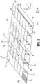
- FIG. 1 is a perspective view of an example artificial magnetic conductor (AMC) antenna in an operational configuration, according to an embodiment.
- AMC antenna 100 (interchangeably, "AMC antenna apparatus 100") may include a ground plane 105, an antenna element layer 130 with at least one antenna element, and an antenna feed (e.g., 300 of FIG. 3 , omitted from FIG. 1 for clarity).
- Ground plane 105 may include: a base layer 110 having a conductive base surface; a frequency selective surface (FSS) layer 120; and a plurality of memory metal wires 115 electrically connecting FSS layer 120 to the conductive base surface.
- elements 115 can be an elongated structure other than a wire such as a memory metal column.
- Ground plane 105 with such a textured surface configuration may be understood as a "high impedance surface” within a given frequency band, in which surface wave modes differ significantly from those on a smooth metallic surface. (Note that the term “frequency selective surface (FSS)" emphasizes the frequency sensitive nature of the high impedance surface.) Ground plane 105 may also be understood as an "in-phase reflector" with suppressed surface waves.
- the textured structure of ground plane 105 enables AMC antenna 100 to be made substantially thinner than traditional ground plane antennas, i.e., non-AMC antennas with a radiating element spaced ⁇ /4 over a ground plane.
- FSS layer 120 includes a plurality of conductive patches 121_1 to 121_n separated from one another by narrow isolation regions ("streets") 123.
- each conductive patch 121 in FIG. 1 may include a conductive surface printed on a thin dielectric sheet such as a polyimide film (e.g., Kapton ® ), and the isolation regions 123 may be regions of the dielectric sheet without a printed conductor.
- conductive patches 121_1 to 121_n along with the dielectric sheet (and in some cases, an additional dielectric sheet on the opposite side of the printed conductor) may collectively form a continuous sheet-like or sandwich-type structure.
- the width of an isolation region 123 is small relative to the area of a conductive patch 121, generating a capacitance between adjacent conductive patches 121 that contributes to forming the high impedance surface.
- Each memory metal wire 115 may be oriented in the z (vertical) direction and electrically connect one of the conductive patches 121 to the conductive base surface of base layer 110, such that a "bed of nails" structure is provided between the base layer 110 and FSS layer 120.
- Each of base layer 110, FSS layer 120 and antenna element layer 130 may be flexible sheet-like structures having major surfaces oriented in the x-y plane.
- Memory metal wires 115 are rigid, as depicted in FIG. 1 , in a memory-shaped state that may occur when ambient temperature is above a threshold ("memory-shape threshold").
- Memory metal wires 115 may be composed of nickel-titanium (NiTi), also known as nitinol, or another suitable shape-memory alloy such as copper-aluminum-nickel or an alloy including copper, iron, zinc and gold.
- NiTi nickel-titanium
- nitinol nickel-titanium
- memory metal wires 115 may mechanically support FSS 120 with respect to base layer 110 in the operational configuration to achieve a fixed spacing therebetween (e.g., a uniform spacing between all regions of FSS 120 and base layer 110).
- Memory metal wires 115 are flexible in a non-memory-shaped state during a non-operational stowage state, discussed and illustrated later, which may be initiated when ambient temperature is below the memory-shape threshold.
- a memory metal wire 115 composed of nitinol changes its state from austenite to martensite when cooled below the memory-shape threshold, enabling the memory metal wire 115 to enter a flexible state.
- FSS layer 120 and antenna element layer 130 may be caused to collapse towards base layer 110, enabling AMC antenna 100 to be stowed in a smaller volume than that occupied in the operational state.
- AMC antenna 100 This facilitates stowage and transportation of AMC antenna 100, and, in some cases, unmanned deployment on a carrier such as an orbital satellite.
- AMC antenna 100 is stowed in a retaining structure rolled up or folded, as described and illustrated below.
- memory metal wires 115 may automatically transform back to austenite, the memory-shaped state.
- the memory-shaped state may be a linear configuration.
- an AMC phenomenon is realizable.
- the AMC phenomenon enables AMC antenna 100 to be significantly thinner than the traditional antenna having a radiating element spaced ⁇ /4 over a ground plane.
- the AMC phenomenon allows for efficient antenna performance with spacing between the antenna element layer 130 and base surface 119 ⁇ ⁇ /4, e.g., in the ⁇ /40 to ⁇ /10 range. Such efficiency may be realized due to in-phase reflection and suppression of surface waves.
- constructive interference occurs between a signal radiated directly into free space by antenna element layer 130 and the same signal initially propagated towards, and then reflected from, ground plane 105.
- an example antenna element is illustrated as a crossed-dipole 135 including a first dipole element 132 and a second dipole element 134 orthogonal to first dipole element 132.
- Other types of antenna elements may be substituted, such as a single dipole, a loop antenna, an array of microstrip patch elements, and so forth.
- the crossed-dipole 135 may be printed on a dielectric sheet, illustrated with a hexagonal shape occupying a smaller surface area than each of FSS layer 120 and base layer 110 in FIG. 1 .
- antenna element layer 130 is coextensive in the x-y plane with each of FSS layer 120 and base layer 110.
- ground plane 105 includes a plurality of dielectric or metallic ribs 117, each oriented longitudinally in the y or x directions, for added structural support of bottom ends of memory metal wires 115.
- Conductive patches 121_1 to 121_n may each be arranged in a lattice and have identical geometries, e.g., all rectangular or all square as depicted, or alternatively all hexagonal, all circular or another suitable shape.
- Conductive patches 121_1 to 121_n may also be configured with identical or substantially identical dimensions (e.g., within manufacturing tolerances) in some embodiments.
- Each conductive patch 121 may electrically connect to a respective memory metal wire 115 through a connection 128 in a central location thereof.
- an input section of base layer 110 may include an input flap 112 and an edge rib 184 for mechanical connection to a retaining structure in some applications.
- a plated through hole 158 may have been formed through rib 117 and base layer 110.
- a bottom end of memory wire 115 may have been inserted within through hole 158 and electrically connected to conductive base surface 119 with a conductive adherent 157 surrounding memory wire 115 within through hole 158, e.g., solder that was melted and cooled.
- FSS layer 120 may include conductive patches 121_1 to 121_n sandwiched between a lower dielectric sheet 154 and an upper dielectric sheet 164. Alternatively, FSS layer 120 is constructed with a single dielectric sheet 154 or 164 with conductive patches 121 printed thereon.
- a mechanical and electrical connection 128 between an upper portion of memory wire 115 and FSS layer 120 may comprise a plated through hole 168, an upper portion of memory wire 115, and a conductive adherent 167 within through hole 168.
- FIG. 2 depicts a single connection 128 between a memory wire 115 and a given conductive patch 121_j, which is separated by respective isolation regions 123 from adjacent conductive patches 121_(j-1) and 121_(j+1).
- Dielectric sheet 164 including isolation regions 123 may have been formed by layered deposition of dielectric material atop conductive patches 121, subsequent to deposition of conductive patches 121 on the upper surface of dielectric sheet 154. However, if dielectric sheet 164 is omitted, isolation regions 123 may be air gaps or a dielectric filler.
- Each of dielectric sheets 144, 154, 164 and 174 may be a polyimide film such as Kapton ® .
- AMC antenna 100 may each be formed at a distance d1 above dielectric sheet 144 (with memory wires in the rigid state).
- FSS layer 120 may be supported by memory wires 115 with its lower surface uniformly spaced throughout by distance d1 from base layer 110.
- An air gap 191 may be present in the regions surrounding memory wires 115.
- Antenna element layer 130 may include the at least one antenna element 132 printed atop dielectric layer 174.
- An example mechanical connection between antenna element layer 130 and FSS layer 120 may include an extension portion 176 of memory wire 115 extending above the upper surface of dielectric sheet 164, a plated blind via 178 in the lower surface of dielectric sheet 174, and an electrically conductive adherent 177 such as solder.
- the upper end of extension 176 may have been inserted within via 178 and adhered to dielectric sheet 174 by melting and cooling adherent 177. All or most of memory wires 115 underlaying antenna element layer 130 may likewise include an extension 176 adhered to dielectric sheet 174 in this manner.
- antenna element layer 130 may be entirely supported by memory wires 115 and uniformly spaced at a distance d2 (with memory wire 115 in the rigid state) from the upper surface of FSS layer 120. It is noted that if antenna layer 130 is only centrally located with respect to FSS layer 120, as in the example of FIG. 1 , then the memory wires 115 located outside the region of antenna layer 130 may omit extensions 176. These peripheral memory wires 115 may all be designed with the same or substantially the same length (e.g., within manufacturing tolerances), and the top ends may be flush with the upper surface of dielectric sheet 164. In a similar vein, each of the memory wires 115 underlaying antenna layer 130 may be identically or substantially identically designed, with extensions 176 of the same or substantially the same length (e.g., within manufacturing tolerances).
- an air gap 171 may exist between layers 120 and 130.
- antenna element layer 130 may be caused to collapse relative to FSS layer 120, whereupon the distance d2 is reduced in the stowed state.
- extensions 176 on memory wires 115 are omitted throughout AMC antenna 100; dielectric sheets 164 and 174 are fused or formed as a single dielectric sheet; and no air gap 171 exists between FSS layer 120 and antenna element layer 130.
- First dipole element 132 includes dipoles arms 132a and 132b; second dipole element 134 includes dipole arms 134a and 134b.
- a second end of first coaxial cable 310 connects to first dipole element 132, with interconnect 317 connecting outer conductor 313 to dipole arm 132a and interconnect 319 connecting inner conductor 311 to dipole arm 132b.
- a second end of second coaxial cable 310 connects to second dipole element 134, with interconnect 327 connecting outer conductor 323 to dipole arm 134a and interconnect 329 connecting inner conductor 321 to dipole arm 134b.
- FIG. 4 is a perspective view depicting an example central portion of an upper part of the AMC antenna 100 of FIG. 1 , illustrating a portion of the example antenna feed 300.
- a central portion of crossed-dipole antenna element 135 may overlay an intersection region of centralized, adjacent conductive patches 121_i, 121_(i+1), 121_(i+2) and 121_(i+3).
- An opening 375 in FSS layer 120 may be formed in the centralized region, by removing a corner piece of each of conductive patches 121_i to 121 (i+3).
- Another opening 385 may have been formed in a centralized region of antenna element layer 130.
- Coaxial cables 310 and 320 may extend vertically (z direction) between antenna element layer 130 and base layer 110 during the deployed state of AMC antenna 100. During the stowage state, coaxial cables may be caused to collapse between antenna element layer 130 and base layer 110.
- Interconnects 317 and 327 may each be embodied as wire bonds.
- interconnects 317 and 327 are in the form of a funnel shaped metal section integrated with a wire extension.
- the funnel shaped metal section is soldered or otherwise electrically connected to the respective outer conductors 313 or 323, and the wire extension is soldered or otherwise electrically connected to an input point of dipole arm 132a or 134a.
- Interconnects 319 and 329 may be direct solder connections to input points of dipole arms 132b and 134b, respectively.
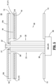
- FIG. 5 is a cross-sectional view taken along the lines 5-5 of FIG. 4 , depicting an example integration of antenna feed 300 within AMC antenna 100.
- This view shows that balun 350 may be disposed adjacent to the lower surface of AMC antenna 100, and the lower ends of coaxial cables 310 and 320 may penetrate an opening 365 in base layer 110 and connect to balun 350.
- Coaxial cables 310 and 320 may run vertically side by side, with upper ends thereof penetrating opening 375 in FSS layer 120 and opening 385 in dielectric sheet 174 of antenna layer 130 to facilitate the electrical connection to crossed-dipole antenna element 135.
- coaxial cables 310 and 320 may be collapsed similar to memory wires 115 (illustrated below in FIG. 8 ).
- FIG. 6 is a perspective view of an example antenna apparatus including a retaining structure retaining an AMC antenna during stowage, according to an embodiment.
- FIG. 7 is a perspective view showing the antenna apparatus of FIG. 6 following removal of the AMC antenna during deployment. The view of FIG. 7 also illustrates an example arrangement of the AMC antenna with respect to the retaining structure prior to insertion therein.
- AMC antenna apparatus 200 includes AMC antenna 100 and retaining structure 210 which retains AMC antenna 100 in a coiled state during stowage.
- Retaining structure 210 in this embodiment is a generally cylindrical structure with first and second opposite end walls 216 and 218, a spindle 225 between end walls 216 and 218, and support rods 228 that couple end walls 216 and 218 to one another.
- Each of end walls 216, 218 may have a spiraling groove 214 on an inner surface 212 thereof to facilitate guiding and retaining AMC antenna 100 in a coiled configuration.
- Opposite edge portions of at least ground plane 105 are retained coiled within the pair of spiraling grooves 214 during stowage. If antenna layer 130 is configured coextensive with ground plane 105, opposite edge portions of antenna layer 130 may also be retained within spiraling grooves 214.
- Spindle 225 may have a mechanical link 272 (shown schematically) to end rib 184 of AMC antenna 100.
- AMC antenna 100 may be forced in a collapsed state as shown in FIG. 7 .
- memory metal wires 115 are flexible and FSS layer 120 is collapsed towards base layer 110 such that the thickness of at least the edge portions of the collapsed structure is thinner than the width of grooves 214.
- FSS layer 120 may be collapsed towards base layer 110 in the +x direction such that FSS layer 120 is offset with respect to base layer 110.
- a peripheral portion 110a of base layer 110 is no longer overlaid by a corresponding portion of FSS layer 120.
- the transition from the operational configuration, e.g., as seen in FIG. 1 , to the collapsed configuration, and vice versa may be analogous to "four bar linkage" mechanical action.
- memory metal wires 115 may be considered analogous to a first pair of bars that transition between vertical and horizontal orientations.
- the plate-like geometries of base layer 110 and FSS layer 120 may be analogous to a second pair of bars, coupled to the first pair of bars, that shift between an aligned condition and an offset condition when the first pair of bars shifts between vertical and horizontal orientations.
- Spindle 225 may be rotated (e.g., clockwise) to draw AMC antenna 100 within retaining structure 210.
- a hand crank (not shown) or an actuator 275 with link 273 may be coupled to an end 219 of spindle 225 to impart a rotational force to draw AMC antenna 100 within retaining structure 210.
- AMC antenna apparatus 200 may be transported to a carrier, such as an orbital satellite prior to launch, and secured to a surface 285 of the carrier.
- retaining structure 210 is more robust to environmental conditions and motion than AMC antenna 100 itself (if otherwise mounted on surface 285 without protection), securing retaining structure 210 to surface 285 prior to deployment of AMC antenna 100 on surface 285 may improve the odds of successful deployment.
- surface 285 is a planetary surface or a surface of a man-made structure on a planet. In this case, retaining structure 210 with AMC antenna 100 secured therein may be transported by a drone and dropped onto surface 285 for subsequent unmanned deployment.
- spindle 225 may be rotated (e.g., counter-clockwise) by actuator 275, whereby AMC antenna 100 may slide out in a plate-like configuration while in its collapsed state in the +x direction.
- actuator 275 may automatically pull out AMC antenna 100 from retaining structure 210.
- AMC antenna 100 may have an opening 129 on the side opposite flap 112, through which a link 262 of actuator 260 may attach to AMC antenna 100.
- actuator 260 and/or actuator 275 may be a robotic arm secured to surface 285.
- AMC antenna 100 is removed from retaining structure 210 in the collapsed state, if ambient temperature is above the memory-shape threshold, memory metal wires 115 may automatically transition from flexible to rigid and orient themselves in the z direction. This transitions AMC antenna 100 from the collapsed state to the operational state, as depicted in FIG. 1 .
- heat may be applied to AMC antenna 100 such to raise the localized temperature surrounding AMC antenna 100 and cause memory wires 115 to transition to the memory-shaped state.
- heat is applied by applying electric current to memory wires 115, whereby the resistance of memory wires 115 while current is flowing produces heat sufficient to cause the transition.
- FIG. 8 is a cross-sectional view of AMC antenna 100 taken along the lines 8-8 of FIG. 7 , illustrating an example structure of AMC antenna 100 in a collapsed state.
- memory wires 115 are flexible may be collapsed with a generally horizontal orientation (generally oriented in the x direction), whereby a spacing distance d3 between base layer 110 and FSS layer 120 is significantly less than the spacing distance d1 as seen in FIG. 2 .
- a spacing distance d4 between FSS layer 120 and antenna layer 130 may be reduced relative to distance d2 ( FIG. 2 ), due to a similar collapse of extensions 176.
- the overall thickness of AMC antenna 100 may be significantly less than that in the operational state, enabling compact retention within a suitable retaining structure.
- FIG. 9 illustrates AMC antenna 100 in a folded state for stowage, whereby transportation of AMC antenna 100 is facilitated.
- AMC antenna 100 To fold AMC antenna 100, it is first set up in the collapsed configuration and thereafter folded at least once.
- a retaining structure in the form of a retaining strap 199 may then retain AMC antenna 100 in the folded state.
- AMC antenna 100 in the folded state may be transported to unmanned carrier surface 285 (shown in FIGS. 6 and 7 ) and secured thereon by suitable fasteners (not shown) coupled to retaining strap 199.
- a robot arm or the like may cut retaining strap 199 and unfold AMC antenna 100.
- AMC antenna 100 may thereafter automatically transition to the operational state, as memory wires 115 transition to their rigid states, in a similar manner as described above (e.g., applying heat).
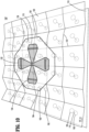
- FIG. 10 is a perspective view depicting an AMC antenna, 100', in a partially deployed state according to another embodiment.
- AMC antenna 100' differs from AMC antenna 100 described above by omitting support ribs 117 and employing an individual support structure for each conductive patch 121 of FSS layer 120.
- FIG. 11 is a cross-sectional view showing an example support structure within the centralized region of AMC antenna 100', i.e., within the region of antenna element layer 130.
- a support structure may include a support 192 attached to base layer 110, a support 193 attached to FSS layer 120, and a support 194 attached to antenna element layer 130.
- Each of supports 192, 193 and 194 may have a button-like profile, occupying a circular area at least one order of magnitude less than the surface area of the corresponding conductive patch 121.
- Each of supports 192-194 may be composed of dielectric material adhered to a respective one of the dielectric sheets in layers 110, 120 or 130.
- Each support 192, 193 and 194 may have a central opening through which a memory wire 115 traverses and is adhered to the respective support. For instance, a plated through hole may have been formed through support 192 and base layer 110 in a similar or identical manner as described above for rib 117 in connection with FIG.
- a similar plated through hole may have been formed in FSS layer 120 and support 193 to adhere a central section of memory wire 115 to support 193.
- a blind via may have been formed through support 194 and dielectric sheet 174 of antenna element layer 130 to adhere an extension 176 of memory wire 115 to support 194 and to antenna element layer 130.
- conductive patch 121_m For peripherally located conductive patches 121 that do not underly antenna element layer 130, such as conductive patch 121_m, only supports 192 and 193 may be utilized, and extensions 176 may be omitted.
- upper ends of memory wires 115 may be flush with the upper surface of FSS layer 120.
- AMC antenna 100' may be the same as those described above for AMC antenna 100.
- AMC antenna 100' may be retained and removed from a retaining structure such as 210 or 199 in a similar manner as described above for AMC antenna 100.
- FIG. 12 is a flow chart depicting operations of an example method, 1200, of deploying an AMC antenna on an unmanned carrier according to an embodiment.
- the AMC antenna e.g., 100 or 100'
- the retaining structure may then be transported with the AMC antenna stored therein to an unmanned carrier (S1220).
- the unmanned carrier e.g., a carrier including surface 285) include an orbital satellite, a planetary surface or a man-made structure on a planetary surface.
- the AMC antenna may then be deployed (S1230) by removing the same from the retaining structure using an actuator (e.g., 275 and/or 260) as described above, and allowing the memory metal wires 115 of the AMC antenna to automatically transition from flexible to rigid states when ambient temperature exceeds the memory-shape threshold.
- the AMC antenna is set up for operation (e.g., in the above-described configuration shown in FIG. 1 ).
- heat may be applied to the AMC antenna to raise the localized temperature surrounding the AMC antenna and cause memory wires 115 to transition to the memory-shaped state.
- Heat may be applied by applying electric current to memory wires 115, whereby the resistance of memory wires 115 while current is flowing produces heat sufficient to cause the transition.
- a robotic arm or the like may secure the AMC antenna to the surface 285 of the carrier, and electrically connect the balun 350 of the AMC antenna to an RF front end of a communication system, whereby active communication of signals by the AMC antenna may be initiated.
Landscapes
- Physics & Mathematics (AREA)
- Engineering & Computer Science (AREA)
- Astronomy & Astrophysics (AREA)
- General Physics & Mathematics (AREA)
- Remote Sensing (AREA)
- Aviation & Aerospace Engineering (AREA)
- Optics & Photonics (AREA)
- Details Of Aerials (AREA)
- Radar Systems Or Details Thereof (AREA)
- Aerials With Secondary Devices (AREA)
- Variable-Direction Aerials And Aerial Arrays (AREA)
Abstract
Description
- This application claims priority to
U.S. Provisional Application No. 63/091,922, filed in the U.S. Patent and Trademark Office on October 14, 2020 - This disclosure relates generally to storage and deployment techniques for antennas with ground planes; and to artificial magnetic conductor (AMC) antennas.
- In a traditional antenna over a ground plane, the radiating element is spaced one quarter wavelength (λ/4) from the ground plane to achieve constructive interference with the reflected signal and thereby increase directivity. At relatively low frequencies, however, the λ/4 distance may be longer than desired, resulting in a thick antenna profile (e.g., 25 cm at 300 MHz).
- With an artificial magnetic conductor (AMC) ground plane, the spacing between the ground plane and the radiating element is significantly smaller, and comparable directivity performance may be realized for the antenna. An AMC ground plane may include a conductive base surface and a "frequency selective surface" (FSS) composed of a plurality of conductive patches separated from one another. The conductive patches may be electrically connected to the base surface through respective wires which are typically embedded within a low loss dielectric. The resulting structure, although thinner than traditional ground plane based antennas, is stiff and burdensome to transport, particularly for large aperture antennas configured for frequencies below 1 GHz.
- In an aspect of the present disclosure, an artificial magnetic conductor (AMC) antenna apparatus includes a ground plane and a flexible antenna element layer including at least one antenna element above the ground plane. The ground plane includes a conductive base surface, a plurality of memory metal wires, and a frequency selective surface (FSS) layer above the base surface, where the FSS layer includes a plurality of conductive patches separated from one another. Each of the memory metal wires electrically connects one of the conductive patches to the base surface. Each of the memory metal wires is rigid in a memory-shaped state, causing the FSS layer to be fixedly spaced from the base surface during operation of the AMC antenna apparatus. The memory metal wires are each flexible in a non-memory-shaped state, enabling the FSS layer to be collapsed towards the base surface when the antenna apparatus is stowed.
- The AMC antenna apparatus may further include a retaining structure configured to retain, when the antenna apparatus is stowed, the antenna element layer and the ground plane with the FSS layer collapsed towards the base surface.
- The retaining structure may retain the antenna element layer and the ground plane in a coiled state.
- The AMC antenna apparatus may further include at least one actuator configured to remove the antenna element layer and the ground plane from the retaining structure.
- In another aspect, a method of deploying an AMC antenna on an unmanned carrier is provided. The AMC antenna includes: (i) an antenna element layer; and (ii) a ground plane with a conductive base surface, an FSS layer, and a plurality of memory metal wires electrically and mechanically coupling the conductive base surface to the FSS layer. The memory metal wires are in a collapsed, non-memory-shaped state when the AMC antenna apparatus is stored. The method involves storing the AMC antenna in a retaining structure; and removing, using an actuator, the AMC antenna from the retaining structure to deploy the AMC antenna. The memory metal wires automatically transform from flexible to rigid states when ambient temperature exceeds a threshold, causing the FSS to be fixedly spaced from the base surface following the removal of the AMC antenna from the retaining structure.
- The above and other aspects and features of the disclosed technology will become more apparent from the following detailed description, taken in conjunction with the accompanying drawings in which like reference characters indicate like elements or features. Various elements of the same or similar type may be distinguished by annexing the reference label with an underscore / dash and second label that distinguishes among the same / similar elements (e.g., _1, _2), or directly annexing the reference label with a second label. However, if a given description uses only the first reference label, it is applicable to any one of the same / similar elements having the same first reference label irrespective of the second label. Elements and features may not be drawn to scale in the drawings.
-
FIG. 1 is a perspective view of an example AMC antenna in an operational configuration, according to an embodiment. -
FIG. 2 is a cross-sectional view taken along the lines 2-2 ofFIG. 1 , depicting an example inter-layer structure of the AMC antenna. -
FIG. 3 is a schematic diagram illustrating an example antenna feed connected to antenna elements of the AMC antenna ofFIG. 1 . -
FIG. 4 is a perspective view of a central portion of an upper part of the AMC antenna ofFIG. 1 , illustrating a portion of the example antenna feed. -
FIG. 5 is a cross-sectional view taken along the lines 5-5 ofFIG. 4 , depicting an example integration of the antenna feed within the AMC antenna. -
FIG. 6 is a perspective view of an example antenna apparatus including a retaining structure retaining the AMC antenna ofFIG. 1 in a coiled configuration during stowage, according to an embodiment. -
FIG. 7 is a perspective view showing the antenna apparatus ofFIG. 6 following removal of the AMC antenna during deployment. -
FIG. 8 is a cross-sectional view of the antenna apparatus ofFIG. 7 taken along the lines 8-8, illustrating a memory metal wire in a collapsed state. -
FIG. 9 illustrates the antenna apparatus ofFIG. 1 in a folded state for stowage. -
FIG. 10 is a perspective view depicting an AMC antenna in a partially deployed state according to another embodiment. -
FIG. 11 is a cross-sectional view of a portion of the AMC antenna ofFIG. 10 . -
FIG. 12 is a flow chart depicting operations of an example method of deploying an AMC antenna on an unmanned carrier according to an embodiment. - The following description, with reference to the accompanying drawings, is provided to assist in a comprehensive understanding of certain exemplary embodiments of the technology disclosed herein for illustrative purposes. The description includes various specific details to assist a person of ordinary skill the art with understanding the technology, but these details are to be regarded as merely illustrative. For the purposes of simplicity and clarity, descriptions of well-known functions and constructions may be omitted when their inclusion may obscure appreciation of the technology by a person of ordinary skill in the art.
-
FIG. 1 is a perspective view of an example artificial magnetic conductor (AMC) antenna in an operational configuration, according to an embodiment. AMC antenna 100 (interchangeably, "AMCantenna apparatus 100") may include aground plane 105, anantenna element layer 130 with at least one antenna element, and an antenna feed (e.g., 300 ofFIG. 3 , omitted fromFIG. 1 for clarity).Ground plane 105 may include: abase layer 110 having a conductive base surface; a frequency selective surface (FSS)layer 120; and a plurality ofmemory metal wires 115 electrically connectingFSS layer 120 to the conductive base surface. In some embodiments,elements 115 can be an elongated structure other than a wire such as a memory metal column.Ground plane 105 with such a textured surface configuration may be understood as a "high impedance surface" within a given frequency band, in which surface wave modes differ significantly from those on a smooth metallic surface. (Note that the term "frequency selective surface (FSS)" emphasizes the frequency sensitive nature of the high impedance surface.)Ground plane 105 may also be understood as an "in-phase reflector" with suppressed surface waves. The textured structure ofground plane 105 enables AMCantenna 100 to be made substantially thinner than traditional ground plane antennas, i.e., non-AMC antennas with a radiating element spaced λ/4 over a ground plane. -
FSS layer 120 includes a plurality of conductive patches 121_1 to 121_n separated from one another by narrow isolation regions ("streets") 123. Note that eachconductive patch 121 inFIG. 1 may include a conductive surface printed on a thin dielectric sheet such as a polyimide film (e.g., Kapton®), and theisolation regions 123 may be regions of the dielectric sheet without a printed conductor. Thus, conductive patches 121_1 to 121_n along with the dielectric sheet (and in some cases, an additional dielectric sheet on the opposite side of the printed conductor) may collectively form a continuous sheet-like or sandwich-type structure. The width of anisolation region 123 is small relative to the area of aconductive patch 121, generating a capacitance between adjacentconductive patches 121 that contributes to forming the high impedance surface. Eachmemory metal wire 115 may be oriented in the z (vertical) direction and electrically connect one of theconductive patches 121 to the conductive base surface ofbase layer 110, such that a "bed of nails" structure is provided between thebase layer 110 andFSS layer 120. Each ofbase layer 110,FSS layer 120 andantenna element layer 130 may be flexible sheet-like structures having major surfaces oriented in the x-y plane. -
Memory metal wires 115 are rigid, as depicted inFIG. 1 , in a memory-shaped state that may occur when ambient temperature is above a threshold ("memory-shape threshold").Memory metal wires 115 may be composed of nickel-titanium (NiTi), also known as nitinol, or another suitable shape-memory alloy such as copper-aluminum-nickel or an alloy including copper, iron, zinc and gold. By virtue of their rigidity in the memory-shaped state,memory metal wires 115 may mechanically support FSS 120 with respect tobase layer 110 in the operational configuration to achieve a fixed spacing therebetween (e.g., a uniform spacing between all regions of FSS 120 and base layer 110).Memory metal wires 115 are flexible in a non-memory-shaped state during a non-operational stowage state, discussed and illustrated later, which may be initiated when ambient temperature is below the memory-shape threshold. For example, amemory metal wire 115 composed of nitinol changes its state from austenite to martensite when cooled below the memory-shape threshold, enabling thememory metal wire 115 to enter a flexible state. When thememory metal wires 115 are flexible,FSS layer 120 andantenna element layer 130 may be caused to collapse towardsbase layer 110, enablingAMC antenna 100 to be stowed in a smaller volume than that occupied in the operational state. This facilitates stowage and transportation ofAMC antenna 100, and, in some cases, unmanned deployment on a carrier such as an orbital satellite. In some examples,AMC antenna 100 is stowed in a retaining structure rolled up or folded, as described and illustrated below. WhenAMC antenna 100 is removed from the retaining structure and ambient temperature exceeds the memory-shape threshold,memory metal wires 115 may automatically transform back to austenite, the memory-shaped state. WithAMC antenna 100, the memory-shaped state may be a linear configuration. - Through suitable design of the number, geometry and layout of
conductive patches 121; the at least one antenna element ofantenna layer 120; the lengths ofmemory metal wires 115; and the spacing betweenantenna element layer 130 andFSS 120, an AMC phenomenon is realizable. As noted, the AMC phenomenon enablesAMC antenna 100 to be significantly thinner than the traditional antenna having a radiating element spaced λ/4 over a ground plane. For instance, the AMC phenomenon allows for efficient antenna performance with spacing between theantenna element layer 130 andbase surface 119 << λ/4, e.g., in the λ/40 to λ/10 range. Such efficiency may be realized due to in-phase reflection and suppression of surface waves. Thus, despite the close spacing between the layers, constructive interference occurs between a signal radiated directly into free space byantenna element layer 130 and the same signal initially propagated towards, and then reflected from,ground plane 105. - In the embodiment of
FIG. 1 , an example antenna element is illustrated as a crossed-dipole 135 including afirst dipole element 132 and asecond dipole element 134 orthogonal tofirst dipole element 132. Other types of antenna elements may be substituted, such as a single dipole, a loop antenna, an array of microstrip patch elements, and so forth. The crossed-dipole 135 may be printed on a dielectric sheet, illustrated with a hexagonal shape occupying a smaller surface area than each ofFSS layer 120 andbase layer 110 inFIG. 1 . In other examples,antenna element layer 130 is coextensive in the x-y plane with each ofFSS layer 120 andbase layer 110. An example construction ofground plane 105 includes a plurality of dielectric ormetallic ribs 117, each oriented longitudinally in the y or x directions, for added structural support of bottom ends ofmemory metal wires 115. Conductive patches 121_1 to 121_n may each be arranged in a lattice and have identical geometries, e.g., all rectangular or all square as depicted, or alternatively all hexagonal, all circular or another suitable shape. Conductive patches 121_1 to 121_n may also be configured with identical or substantially identical dimensions (e.g., within manufacturing tolerances) in some embodiments. Eachconductive patch 121 may electrically connect to a respectivememory metal wire 115 through aconnection 128 in a central location thereof. Note that an input section ofbase layer 110 may include aninput flap 112 and anedge rib 184 for mechanical connection to a retaining structure in some applications. -
FIG. 2 is a cross-sectional view taken along the lines 2-2 ofFIG. 1 , and depicts an example inter-layer structure ofAMC antenna 100 during an operational (deployed) state. (InFIG. 2 and other cross-sectional views herein, features located behind those illustrated may be omitted for clarity.)Base layer 110 may include aconductive base surface 119 adhered to or printed at a bottom surface of aflexible dielectric sheet 144 for structural integrity and to facilitate electrical and mechanical connections to memory metal wires 115 (interchangeably, "memory wires" 115). Adielectric rib 117 may be adhered to a top surface ofdielectric sheet 144 and support a connection of amemory wire 115 tobase surface 119. A plated throughhole 158 may have been formed throughrib 117 andbase layer 110. A bottom end ofmemory wire 115 may have been inserted within throughhole 158 and electrically connected toconductive base surface 119 with aconductive adherent 157 surroundingmemory wire 115 within throughhole 158, e.g., solder that was melted and cooled. -
FSS layer 120 may include conductive patches 121_1 to 121_n sandwiched between a lowerdielectric sheet 154 and anupper dielectric sheet 164. Alternatively,FSS layer 120 is constructed with asingle dielectric sheet conductive patches 121 printed thereon. A mechanical andelectrical connection 128 between an upper portion ofmemory wire 115 andFSS layer 120 may comprise a plated throughhole 168, an upper portion ofmemory wire 115, and aconductive adherent 167 within throughhole 168.FIG. 2 depicts asingle connection 128 between amemory wire 115 and a given conductive patch 121_j, which is separated byrespective isolation regions 123 from adjacent conductive patches 121_(j-1) and 121_(j+1).Dielectric sheet 164 includingisolation regions 123 may have been formed by layered deposition of dielectric material atopconductive patches 121, subsequent to deposition ofconductive patches 121 on the upper surface ofdielectric sheet 154. However, ifdielectric sheet 164 is omitted,isolation regions 123 may be air gaps or a dielectric filler. Each ofdielectric sheets -
Electrical connections 128 throughoutAMC antenna 100 may each be formed at a distance d1 above dielectric sheet 144 (with memory wires in the rigid state). In this manner,FSS layer 120 may be supported bymemory wires 115 with its lower surface uniformly spaced throughout by distance d1 frombase layer 110. Anair gap 191 may be present in the regions surroundingmemory wires 115. -
Antenna element layer 130 may include the at least oneantenna element 132 printed atopdielectric layer 174. An example mechanical connection betweenantenna element layer 130 andFSS layer 120 may include anextension portion 176 ofmemory wire 115 extending above the upper surface ofdielectric sheet 164, a plated blind via 178 in the lower surface ofdielectric sheet 174, and an electricallyconductive adherent 177 such as solder. The upper end ofextension 176 may have been inserted within via 178 and adhered todielectric sheet 174 by melting and coolingadherent 177. All or most ofmemory wires 115 underlayingantenna element layer 130 may likewise include anextension 176 adhered todielectric sheet 174 in this manner. As a result,antenna element layer 130 may be entirely supported bymemory wires 115 and uniformly spaced at a distance d2 (withmemory wire 115 in the rigid state) from the upper surface ofFSS layer 120. It is noted that ifantenna layer 130 is only centrally located with respect toFSS layer 120, as in the example ofFIG. 1 , then thememory wires 115 located outside the region ofantenna layer 130 may omitextensions 176. Theseperipheral memory wires 115 may all be designed with the same or substantially the same length (e.g., within manufacturing tolerances), and the top ends may be flush with the upper surface ofdielectric sheet 164. In a similar vein, each of thememory wires 115underlaying antenna layer 130 may be identically or substantially identically designed, withextensions 176 of the same or substantially the same length (e.g., within manufacturing tolerances). - With the above-described mechanical connection between
FSS layer 120 andantenna element layer 130, anair gap 171 may exist betweenlayers memory wires 115 are in the non-memory metal shaped state (flexible state),antenna element layer 130 may be caused to collapse relative toFSS layer 120, whereupon the distance d2 is reduced in the stowed state. In an alternative configuration,extensions 176 onmemory wires 115 are omitted throughoutAMC antenna 100;dielectric sheets air gap 171 exists betweenFSS layer 120 andantenna element layer 130. -
FIG. 3 is a schematic diagram illustrating an example antenna feed, 300, that may connect toantenna element 135 of theAMC antenna 100.Antenna feed 300 may include abalun 350; a first flexiblecoaxial cable 310 having a first end connected to balun 350 and having anouter conductor 313 and aninner conductor 311; a second flexiblecoaxial cable 320 having a first end connected to balun 350 and having anouter conductor 323 and aninner conductor 321; and first, second, third andfourth interconnects First dipole element 132 includesdipoles arms second dipole element 134 includesdipole arms coaxial cable 310 connects tofirst dipole element 132, withinterconnect 317 connectingouter conductor 313 todipole arm 132a and interconnect 319 connectinginner conductor 311 todipole arm 132b. A second end of secondcoaxial cable 310 connects tosecond dipole element 134, withinterconnect 327 connectingouter conductor 323 todipole arm 134a and interconnect 329 connectinginner conductor 321 todipole arm 134b. -
FIG. 4 is a perspective view depicting an example central portion of an upper part of theAMC antenna 100 ofFIG. 1 , illustrating a portion of theexample antenna feed 300. A central portion of crossed-dipole antenna element 135 may overlay an intersection region of centralized, adjacent conductive patches 121_i, 121_(i+1), 121_(i+2) and 121_(i+3). Anopening 375 inFSS layer 120 may be formed in the centralized region, by removing a corner piece of each of conductive patches 121_i to 121 (i+3). Anotheropening 385 may have been formed in a centralized region ofantenna element layer 130.Coaxial cables antenna element layer 130 andbase layer 110 during the deployed state ofAMC antenna 100. During the stowage state, coaxial cables may be caused to collapse betweenantenna element layer 130 andbase layer 110. - The second ends of
coaxial cables opening 385.Interconnects outer conductors dipole arm Interconnects dipole arms -
FIG. 5 is a cross-sectional view taken along the lines 5-5 ofFIG. 4 , depicting an example integration ofantenna feed 300 withinAMC antenna 100. This view shows thatbalun 350 may be disposed adjacent to the lower surface ofAMC antenna 100, and the lower ends ofcoaxial cables opening 365 inbase layer 110 and connect tobalun 350.Coaxial cables opening 375 inFSS layer 120 andopening 385 indielectric sheet 174 ofantenna layer 130 to facilitate the electrical connection to crossed-dipole antenna element 135. In the stowed state,coaxial cables FIG. 8 ). -
FIG. 6 is a perspective view of an example antenna apparatus including a retaining structure retaining an AMC antenna during stowage, according to an embodiment.FIG. 7 is a perspective view showing the antenna apparatus ofFIG. 6 following removal of the AMC antenna during deployment. The view ofFIG. 7 also illustrates an example arrangement of the AMC antenna with respect to the retaining structure prior to insertion therein. Referring toFIGS. 6 and7 ,AMC antenna apparatus 200 includesAMC antenna 100 and retainingstructure 210 which retainsAMC antenna 100 in a coiled state during stowage. Retainingstructure 210 in this embodiment is a generally cylindrical structure with first and secondopposite end walls spindle 225 betweenend walls support rods 228 thatcouple end walls end walls groove 214 on aninner surface 212 thereof to facilitate guiding and retainingAMC antenna 100 in a coiled configuration. Opposite edge portions of at leastground plane 105 are retained coiled within the pair of spiralinggrooves 214 during stowage. Ifantenna layer 130 is configured coextensive withground plane 105, opposite edge portions ofantenna layer 130 may also be retained within spiralinggrooves 214. -
Spindle 225 may have a mechanical link 272 (shown schematically) to endrib 184 ofAMC antenna 100. To initially retainAMC antenna 100 within retainingstructure 210,AMC antenna 100 may be forced in a collapsed state as shown inFIG. 7 . In the collapsed state,memory metal wires 115 are flexible andFSS layer 120 is collapsed towardsbase layer 110 such that the thickness of at least the edge portions of the collapsed structure is thinner than the width ofgrooves 214. Note that in the collapsed state,FSS layer 120 may be collapsed towardsbase layer 110 in the +x direction such thatFSS layer 120 is offset with respect tobase layer 110. Because the two layers are offset in the collapsed condition, aperipheral portion 110a ofbase layer 110 is no longer overlaid by a corresponding portion ofFSS layer 120. For instance, the transition from the operational configuration, e.g., as seen inFIG. 1 , to the collapsed configuration, and vice versa may be analogous to "four bar linkage" mechanical action. In other words,memory metal wires 115 may be considered analogous to a first pair of bars that transition between vertical and horizontal orientations. The plate-like geometries ofbase layer 110 andFSS layer 120 may be analogous to a second pair of bars, coupled to the first pair of bars, that shift between an aligned condition and an offset condition when the first pair of bars shifts between vertical and horizontal orientations. -
Spindle 225 may be rotated (e.g., clockwise) to drawAMC antenna 100 within retainingstructure 210. As an example, a hand crank (not shown) or anactuator 275 withlink 273 may be coupled to anend 219 ofspindle 225 to impart a rotational force to drawAMC antenna 100 within retainingstructure 210. OnceAMC antenna 100 is retained within retainingstructure 210,AMC antenna apparatus 200 may be transported to a carrier, such as an orbital satellite prior to launch, and secured to asurface 285 of the carrier. Since retainingstructure 210 is more robust to environmental conditions and motion thanAMC antenna 100 itself (if otherwise mounted onsurface 285 without protection), securing retainingstructure 210 to surface 285 prior to deployment ofAMC antenna 100 onsurface 285 may improve the odds of successful deployment. As another example,surface 285 is a planetary surface or a surface of a man-made structure on a planet. In this case, retainingstructure 210 withAMC antenna 100 secured therein may be transported by a drone and dropped ontosurface 285 for subsequent unmanned deployment. - To deploy
AMC antenna 100 from retainingstructure 210,spindle 225 may be rotated (e.g., counter-clockwise) byactuator 275, wherebyAMC antenna 100 may slide out in a plate-like configuration while in its collapsed state in the +x direction. Alternatively or additionally, anotheractuator 260 arranged onsurface 285 may automatically pull outAMC antenna 100 from retainingstructure 210. To this end,AMC antenna 100 may have anopening 129 on the side oppositeflap 112, through which alink 262 ofactuator 260 may attach toAMC antenna 100. Note thatactuator 260 and/oractuator 275 may be a robotic arm secured to surface 285. OnceAMC antenna 100 is removed from retainingstructure 210 in the collapsed state, if ambient temperature is above the memory-shape threshold,memory metal wires 115 may automatically transition from flexible to rigid and orient themselves in the z direction. This transitionsAMC antenna 100 from the collapsed state to the operational state, as depicted inFIG. 1 . In an example, if ambient temperature is below the memory-shape threshold, heat may be applied toAMC antenna 100 such to raise the localized temperature surroundingAMC antenna 100 and causememory wires 115 to transition to the memory-shaped state. In one example, heat is applied by applying electric current tomemory wires 115, whereby the resistance ofmemory wires 115 while current is flowing produces heat sufficient to cause the transition. -
FIG. 8 is a cross-sectional view ofAMC antenna 100 taken along the lines 8-8 ofFIG. 7 , illustrating an example structure ofAMC antenna 100 in a collapsed state. WhenAMC antenna 100 is collapsed for stowage,memory wires 115 are flexible may be collapsed with a generally horizontal orientation (generally oriented in the x direction), whereby a spacing distance d3 betweenbase layer 110 andFSS layer 120 is significantly less than the spacing distance d1 as seen inFIG. 2 . In addition, a spacing distance d4 betweenFSS layer 120 andantenna layer 130 may be reduced relative to distance d2 (FIG. 2 ), due to a similar collapse ofextensions 176. Accordingly, the overall thickness ofAMC antenna 100 may be significantly less than that in the operational state, enabling compact retention within a suitable retaining structure. -
FIG. 9 illustratesAMC antenna 100 in a folded state for stowage, whereby transportation ofAMC antenna 100 is facilitated. To foldAMC antenna 100, it is first set up in the collapsed configuration and thereafter folded at least once. A retaining structure in the form of a retainingstrap 199 may then retainAMC antenna 100 in the folded state. As an example,AMC antenna 100 in the folded state may be transported to unmanned carrier surface 285 (shown inFIGS. 6 and7 ) and secured thereon by suitable fasteners (not shown) coupled to retainingstrap 199. For subsequent deployment ofAMC antenna 100, a robot arm or the like may cut retainingstrap 199 and unfoldAMC antenna 100.AMC antenna 100 may thereafter automatically transition to the operational state, asmemory wires 115 transition to their rigid states, in a similar manner as described above (e.g., applying heat). -
FIG. 10 is a perspective view depicting an AMC antenna, 100', in a partially deployed state according to another embodiment. AMC antenna 100' differs fromAMC antenna 100 described above by omittingsupport ribs 117 and employing an individual support structure for eachconductive patch 121 ofFSS layer 120.FIG. 11 is a cross-sectional view showing an example support structure within the centralized region of AMC antenna 100', i.e., within the region ofantenna element layer 130. Forconductive patches 121 underlaying the region ofantenna layer 130, a support structure may include asupport 192 attached tobase layer 110, asupport 193 attached toFSS layer 120, and asupport 194 attached toantenna element layer 130. Each ofsupports conductive patch 121. Each of supports 192-194 may be composed of dielectric material adhered to a respective one of the dielectric sheets inlayers support memory wire 115 traverses and is adhered to the respective support. For instance, a plated through hole may have been formed throughsupport 192 andbase layer 110 in a similar or identical manner as described above forrib 117 in connection withFIG. 2 , and the lower end ofmemory wire 115 may be soldered to support 192 and tobase layer 110 using solder within the plated through hole. A similar plated through hole may have been formed inFSS layer 120 andsupport 193 to adhere a central section ofmemory wire 115 to support 193. Moreover, a blind via may have been formed throughsupport 194 anddielectric sheet 174 ofantenna element layer 130 to adhere anextension 176 ofmemory wire 115 to support 194 and toantenna element layer 130. For peripherally locatedconductive patches 121 that do not underlyantenna element layer 130, such as conductive patch 121_m, only supports 192 and 193 may be utilized, andextensions 176 may be omitted. Thus, upper ends ofmemory wires 115 may be flush with the upper surface ofFSS layer 120. - Other aspects of AMC antenna 100' may be the same as those described above for
AMC antenna 100. AMC antenna 100' may be retained and removed from a retaining structure such as 210 or 199 in a similar manner as described above forAMC antenna 100. -
FIG. 12 is a flow chart depicting operations of an example method, 1200, of deploying an AMC antenna on an unmanned carrier according to an embodiment. Withmethod 1200, the AMC antenna, e.g., 100 or 100', is first stored in its collapsed state in a retaining structure such as 210 or 199 described above (S1210). The retaining structure may then be transported with the AMC antenna stored therein to an unmanned carrier (S1220). As mentioned earlier, some examples of the unmanned carrier (e.g., a carrier including surface 285) include an orbital satellite, a planetary surface or a man-made structure on a planetary surface. - The AMC antenna may then be deployed (S1230) by removing the same from the retaining structure using an actuator (e.g., 275 and/or 260) as described above, and allowing the
memory metal wires 115 of the AMC antenna to automatically transition from flexible to rigid states when ambient temperature exceeds the memory-shape threshold. When the transition to rigid states is complete, the AMC antenna is set up for operation (e.g., in the above-described configuration shown inFIG. 1 ). As noted above, if ambient temperature during deployment is below the memory-shape threshold, heat may be applied to the AMC antenna to raise the localized temperature surrounding the AMC antenna and causememory wires 115 to transition to the memory-shaped state. Heat may be applied by applying electric current tomemory wires 115, whereby the resistance ofmemory wires 115 while current is flowing produces heat sufficient to cause the transition. With the AMC antenna in an operational configuration, a robotic arm or the like may secure the AMC antenna to thesurface 285 of the carrier, and electrically connect thebalun 350 of the AMC antenna to an RF front end of a communication system, whereby active communication of signals by the AMC antenna may be initiated. - While the technology described herein has been particularly shown and described with reference to example embodiments thereof, it will be understood by those of ordinary skill in the art that various changes in form and details may be made therein without departing from the spirit and scope of the claimed subject matter as defined by the following claims and their equivalents. The disclosure comprises the following items:
- 1. An artificial magnetic conductor (AMC) antenna apparatus (100, 200, 100') comprising:
- a ground plane (105) comprising:
- a conductive base surface (119);
- a frequency selective surface (FSS) layer (120) above the base surface, the FSS layer comprising a plurality of conductive patches (121_1 - 121_n) separated from one another; and
- a plurality of memory metal wires (115), each electrically connecting one of the conductive patches to the base surface and each being rigid in a memory-shaped state, causing the FSS layer to be fixedly spaced from the base surface during operation of the AMC antenna apparatus, and each being flexible in a non-memory-shaped state, enabling the FSS layer to be collapsed towards the base surface when the antenna apparatus is stowed; and
- a flexible antenna element layer (130) above the FSS layer, comprising at least one antenna element (135).
- a ground plane (105) comprising:
- 2. The AMC antenna apparatus (100, 200, 100') of
item 1, wherein:- the plurality of conductive patches is a plurality of printed conductive patches on a first dielectric sheet (154); and
- the at least one antenna element is at least one printed conductive element (135) on a second dielectric sheet (174);
- wherein each of the first and second dielectric sheets is flexible.
- 3. The AMC antenna apparatus (100, 200, 100') of
item 2, wherein;- each of the memory metal wires has a substantially identical length, such that the FSS layer is uniformly spaced from the base surface; and
- the first dielectric sheet is mechanically coupled to the second dielectric sheet such that the antenna element layer is uniformly spaced from the FSS layer.
- 4. The AMC antenna apparatus (100, 200, 100') of
item 3, wherein the memory metal wires include respective extensions (176) that extend above the FSS layer, and the first dielectric sheet is mechanically coupled to the second dielectric sheet and uniformly spaced therefrom by the extensions when the memory metal wires are rigid in the memory-shaped state. - 5. The AMC antenna apparatus (200) of
item 1, further comprising a retaining structure (210) configured to retain, when the antenna apparatus is stowed, the antenna element layer and the ground plane with the FSS layer collapsed towards the base surface. - 6. The AMC antenna apparatus (200) of
item 5, further comprising at least one actuator (275, 260) configured to remove the antenna element layer and the ground plane from the retaining structure. - 7. The AMC antenna apparatus (200) of
item 5, wherein the retaining structure (210) retains the antenna element layer and the ground plane in a coiled state. - 8. The AMC antenna apparatus (200) of item 7, wherein the retaining structure (210) is a cylindrical structure comprising a pair of spiraling grooves (214) in respective opposite ends, wherein opposite edge portions of the ground plane are retained coiled within the pair of spiraling grooves.
- 9. The AMC antenna apparatus (100, 200, 100') of
item 1, wherein the memory metal wires (115) are composed of nitinol. - 10. The AMC antenna apparatus (100, 200, 100') of
item 1, further comprising a flexible antenna feed (310, 320) having a first end electrically connecting to the at least one antenna element, an opposite end below the base surface, and a central portion extending between the base surface and the at least one antenna element through at least one opening (375) in the FSS layer. - 11. The AMC antenna apparatus (100, 200, 100') of item 10, further comprising a balun (350) disposed below the base surface and connected to the opposite end of the antenna feed.
- 12. The AMC antenna apparatus (100, 200, 100') of item 10, wherein the antenna feed comprises at least one flexible coaxial cable (310, 320) having a linear shape when the memory metal wires are in the memory-shaped state and having a collapsed, nonlinear configuration when the memory metal wires are in the non-memory-shaped state.
- 13. The AMC antenna apparatus (100, 200, 100') of
item 1, wherein the at least one antenna element comprises at least one crossed-dipole antenna element (135). - 14. The AMC antenna apparatus (100, 100') of
item 1, wherein the ground plane and the antenna element layer are each folded when the antenna apparatus is stowed. - 15. The AMC antenna apparatus (100, 200, 100') of
item 1, wherein the base surface comprises printed conductive material (119) on a flexible substrate (144). - 16. The AMC antenna apparatus (100, 200, 100') of
item 1, further comprising a plurality of support structures (117, 192) each supporting a mechanical connection between one of the memory metal wires and the base surface and/or one of the conductive patches. - 17. A method (1200) of deploying an artificial magnetic conductor (AMC) antenna (100, 100') on an unmanned carrier (285), the method comprising:
- storing (S1210) the AMC antenna in a retaining structure (210, 199), the AMC antenna comprising: (i) an antenna element layer; and (ii) a ground plane with a conductive base surface, a frequency selective surface (FSS) layer, and a plurality of memory metal wires electrically and mechanically coupling the conductive base surface to the FSS layer, the plurality of memory metal wires being in a collapsed, non-memory-shaped state when the AMC antenna is stored; and
- removing (S1230), using an actuator (260, 275), the AMC antenna from the retaining structure to deploy the AMC antenna,
- wherein the memory metal wires automatically transform from flexible to rigid states when ambient temperature exceeds a threshold, causing the FSS layer to be fixedly spaced from the base surface following the removal of the AMC antenna from the retaining structure.
- 18. The method (1200) of item 17, wherein the unmanned carrier is an orbital satellite (285).
- 19. The method (1200) of item 17, wherein the retaining structure retains the AMC antenna in a coiled state, and the actuator causing the AMC antenna to be rolled out of the retaining structure in a plate-like shape.
- 20. The method (1200) of item 19, wherein the AMC antenna further comprises a flexible antenna feed stored in a coiled shape within the retaining structure and unrolling during the removal of the AMC antenna.
Claims (15)
- An artificial magnetic conductor, AMC, antenna apparatus comprising:a base layer;a frequency selective surface, FSS, layer comprising a plurality of conductive patches separated from one another by one or more isolation regions;a plurality of elongated structures, each electrically connecting a respective one of the conductive patches to the base layer and each being rigid in a first state at an ambient temperature; andan antenna layer comprising at least one antenna element,wherein the FSS layer is fixedly spaced from the base layer when the elongated structures are in the first state and the base layer and the FSS layer are substantially coextensive.
- The AMC antenna apparatus of claim 1, wherein:the plurality of conductive patches is a plurality of printed conductive patches on a first dielectric sheet;the at least one antenna element is at least one printed conductive element on a second dielectric sheet;each of the first and second dielectric sheets is flexible; andthe FSS layer is collapsable towards the base layer when the elongated structures are in a second state different from the first state.
- The AMC antenna apparatus of claim 2, further comprising a flexible antenna feed having a first end electrically connecting to the at least one antenna element, an opposite end below the base layer, and a central portion extending between the base layer and the at least one antenna element through at least one opening in the FSS layer, and optionally wherein the AMC antenna apparatus further comprises a balun disposed below the base layer and connected to the opposite end of the antenna feed.
- The AMC antenna apparatus of claim 3, wherein the antenna feed comprises at least one flexible coaxial cable having a linear shape when the elongated structures are in the second state and having a collapsed, nonlinear configuration when the elongated structures are in the first state.
- The AMC antenna apparatus of claim 2, wherein;each of the elongated structures has a substantially identical length, such that the FSS layer is uniformly spaced from the base layer; andthe first dielectric sheet is mechanically coupled to the second dielectric sheet such that the antenna layer is uniformly spaced from the FSS layer.
- The AMC antenna apparatus of claim 5, wherein the elongated structures include respective extensions that extend above the FSS layer, and the first dielectric sheet is mechanically coupled to the second dielectric sheet and uniformly spaced therefrom by the extensions when the plurality of elongated structures are rigid in the first state.
- The AMC antenna apparatus of claim 2, wherein the at least one antenna element comprises at least one crossed-dipole antenna element.
- The AMC antenna apparatus of claim 1, wherein the FSS layer comprises a plated through hole and a conductive adherent for each elongated structure and/or wherein the elongated structures are composed of nitinol.
- The AMC antenna apparatus of claim 2, wherein an air gap exists between the base layer and the FSS layer when the elongated structures are in the second state.
- The AMC antenna apparatus of claim 1, wherein the base layer and the FSS layer are configured to be stored in a retaining structure when in a coiled state, or wherein the base layer and the FSS layer are each folded when the AMC antenna apparatus is stowed.
- The AMC antenna apparatus of claim 1, wherein the base layer comprises printed conductive material on a flexible substrate.
- The AMC antenna apparatus of claim 1, further comprising a plurality of support structures each supporting a mechanical connection between one of the elongated structures and the base layer and/or one of the conductive patches.
- A method of deploying an artificial magnetic conductor, AMC, antenna apparatus on an unmanned carrier, the method comprising:storing the AMC antenna apparatus in a retaining structure, the AMC antenna apparatus comprising: (i) an antenna layer; and (ii) a ground plane with a conductive base layer, a frequency selective surface, FSS, layer, and a plurality of elongated structures electrically and mechanically coupling the base layer to the FSS layer, the elongated structures being in a collapsed state when the conductor apparatus is stored; andremoving, using an actuator, the AMC antenna apparatus from the retaining structure to deploy the AMC antenna apparatus,wherein the elongated structures automatically transform from the collapsed state to a rigid state when ambient temperature exceeds a threshold, causing the FSS layer to be fixedly spaced from the base layer following the removal of the AMC antenna apparatus from the retaining structure.
- The method of claim 13, wherein the unmanned carrier is an orbital satellite.
- The method of claim 13, wherein the retaining structure retains the AMC antenna apparatus in a coiled state, and the actuator causing the AMC antenna apparatus to be rolled out of the retaining structure in a plate-like shape, and optionally wherein the AMC antenna apparatus further comprises a flexible antenna feed stored in a coiled shape within the retaining structure and unrolling during the removal of the AMC antenna apparatus.
Applications Claiming Priority (3)
| Application Number | Priority Date | Filing Date | Title |
|---|---|---|---|
| US202063091922P | 2020-10-14 | 2020-10-14 | |
| PCT/US2021/054938 WO2022081817A1 (en) | 2020-10-14 | 2021-10-14 | Antenna apparatus and deployment method employing collapsible memory metal |
| EP21805744.6A EP4218092B1 (en) | 2020-10-14 | 2021-10-14 | Antenna apparatus and deployment method employing collapsible memory metal |
Related Parent Applications (1)
| Application Number | Title | Priority Date | Filing Date |
|---|---|---|---|
| EP21805744.6A Division EP4218092B1 (en) | 2020-10-14 | 2021-10-14 | Antenna apparatus and deployment method employing collapsible memory metal |
Publications (2)
| Publication Number | Publication Date |
|---|---|
| EP4432475A2 true EP4432475A2 (en) | 2024-09-18 |
| EP4432475A3 EP4432475A3 (en) | 2024-12-11 |
Family
ID=78536614
Family Applications (2)
| Application Number | Title | Priority Date | Filing Date |
|---|---|---|---|
| EP24179185.4A Pending EP4432475A3 (en) | 2020-10-14 | 2021-10-14 | Antenna apparatus and deployment method employing collapsible memory metal |
| EP21805744.6A Active EP4218092B1 (en) | 2020-10-14 | 2021-10-14 | Antenna apparatus and deployment method employing collapsible memory metal |
Family Applications After (1)
| Application Number | Title | Priority Date | Filing Date |
|---|---|---|---|
| EP21805744.6A Active EP4218092B1 (en) | 2020-10-14 | 2021-10-14 | Antenna apparatus and deployment method employing collapsible memory metal |
Country Status (10)
| Country | Link |
|---|---|
| US (2) | US11923608B2 (en) |
| EP (2) | EP4432475A3 (en) |
| JP (1) | JP2023548668A (en) |
| KR (2) | KR102894456B1 (en) |
| CN (1) | CN116636085B (en) |
| AU (2) | AU2021360929B2 (en) |
| CA (1) | CA3195485A1 (en) |
| IL (1) | IL302044B2 (en) |
| MX (1) | MX2023004284A (en) |
| WO (1) | WO2022081817A1 (en) |
Families Citing this family (3)
| Publication number | Priority date | Publication date | Assignee | Title |
|---|---|---|---|---|
| JP6926174B2 (en) * | 2019-11-26 | 2021-08-25 | 京セラ株式会社 | Antennas, wireless communication modules and wireless communication devices |
| CN117438788A (en) * | 2022-07-12 | 2024-01-23 | 康普技术有限责任公司 | Radiating elements for base station antennas and base station antennas |
| CN119280582B (en) * | 2024-12-16 | 2026-02-17 | 山东省立第三医院 | Portable surgical hand disinfection sprayer |
Family Cites Families (16)
| Publication number | Priority date | Publication date | Assignee | Title |
|---|---|---|---|---|
| JP3611409B2 (en) * | 1996-09-25 | 2005-01-19 | Necトーキン株式会社 | Electric field sensor |
| US6690327B2 (en) * | 2001-09-19 | 2004-02-10 | Etenna Corporation | Mechanically reconfigurable artificial magnetic conductor |
| US6882318B2 (en) * | 2002-03-04 | 2005-04-19 | Siemens Information & Communications Mobile, Llc | Broadband planar inverted F antenna |
| US20070200763A1 (en) * | 2006-02-28 | 2007-08-30 | Harris Corporation | Phased array antenna including flexible layers and associated methods |
| US20080181097A1 (en) * | 2006-11-16 | 2008-07-31 | Interdigital Technology Corporation | Method and ofdm receiver with multi-dimensional window processing unit for robustly decoding rf signals |
| US8274443B2 (en) * | 2009-03-16 | 2012-09-25 | Raytheon Company | Light weight stowable phased array lens antenna assembly |
| KR101115331B1 (en) * | 2009-12-03 | 2012-03-13 | 주식회사 이엠따블유 | Frequency selective surface filter and repeater antenna system for comprising the same |
| KR20120104855A (en) * | 2011-03-14 | 2012-09-24 | 한국전자통신연구원 | Deployable reflectarray antenna |
| US9431709B2 (en) * | 2012-04-03 | 2016-08-30 | Wemtec, Inc. | Artificial magnetic conductor antennas with shielded feedlines |
| LT6384B (en) * | 2015-04-30 | 2017-04-25 | Vilniaus Universitetas | Easyly deployable phased antenna fro a spacecraft and system of such antennas |
| CN110021814B (en) * | 2018-01-08 | 2024-01-30 | 弗莱克斯有限公司 | Planar antenna |
| US20200044326A1 (en) * | 2018-08-03 | 2020-02-06 | Kymeta Corporation | Composite stack-up for flat panel metamaterial antenna |
| US11043729B2 (en) * | 2019-02-05 | 2021-06-22 | Best Medical Canada Ltd. | Flexible antenna for a wireless radiation dosimeter |
| CN110233335B (en) * | 2019-05-09 | 2020-09-04 | 哈尔滨工业大学 | Broadband miniaturization low-profile dual-polarized antenna based on artificial magnetic conductor |
| CN110828964B (en) * | 2019-09-30 | 2022-03-04 | 中国空间技术研究院 | Torsion spring driven single-layer regular hexagon conical deployable truss antenna structure |
| US11128033B1 (en) * | 2020-04-08 | 2021-09-21 | The Boeing Company | Impact recoverable antennas |
-
2021
- 2021-10-14 CA CA3195485A patent/CA3195485A1/en active Pending
- 2021-10-14 KR KR1020237015473A patent/KR102894456B1/en active Active
- 2021-10-14 US US18/250,684 patent/US11923608B2/en active Active
- 2021-10-14 JP JP2023522405A patent/JP2023548668A/en active Pending
- 2021-10-14 MX MX2023004284A patent/MX2023004284A/en unknown
- 2021-10-14 EP EP24179185.4A patent/EP4432475A3/en active Pending
- 2021-10-14 EP EP21805744.6A patent/EP4218092B1/en active Active
- 2021-10-14 IL IL302044A patent/IL302044B2/en unknown
- 2021-10-14 AU AU2021360929A patent/AU2021360929B2/en active Active
- 2021-10-14 WO PCT/US2021/054938 patent/WO2022081817A1/en not_active Ceased
- 2021-10-14 CN CN202180078864.3A patent/CN116636085B/en active Active
- 2021-10-14 KR KR1020257039809A patent/KR20250172905A/en active Pending
-
2024
- 2024-02-05 US US18/432,664 patent/US20240297442A1/en active Pending
-
2026
- 2026-01-07 AU AU2026200090A patent/AU2026200090A1/en active Pending
Also Published As
| Publication number | Publication date |
|---|---|
| US11923608B2 (en) | 2024-03-05 |
| KR102894456B1 (en) | 2025-12-03 |
| AU2021360929B2 (en) | 2025-10-16 |
| EP4432475A3 (en) | 2024-12-11 |
| KR20250172905A (en) | 2025-12-09 |
| CN116636085B (en) | 2026-04-24 |
| IL302044A (en) | 2023-06-01 |
| CA3195485A1 (en) | 2022-04-21 |
| IL302044B1 (en) | 2026-01-01 |
| AU2021360929A9 (en) | 2024-09-26 |
| JP2023548668A (en) | 2023-11-20 |
| KR20230085160A (en) | 2023-06-13 |
| WO2022081817A1 (en) | 2022-04-21 |
| EP4218092B1 (en) | 2024-07-10 |
| IL302044B2 (en) | 2026-05-01 |
| EP4218092A1 (en) | 2023-08-02 |
| CN116636085A (en) | 2023-08-22 |
| US20240297442A1 (en) | 2024-09-05 |
| AU2026200090A1 (en) | 2026-01-22 |
| AU2021360929A1 (en) | 2023-06-08 |
| US20230307843A1 (en) | 2023-09-28 |
| MX2023004284A (en) | 2023-06-22 |
Similar Documents
| Publication | Publication Date | Title |
|---|---|---|
| US20240297442A1 (en) | Antenna apparatus and deployment method employing collapsible memory metal | |
| JP4787248B2 (en) | Antenna radiator structure | |
| US20250174872A1 (en) | Deployable antenna apparatus with inflate to latch mechanism | |
| BR112023006897B1 (en) | Artificial Magnetic Conductor Antenna Apparatus and Method for Implanting an Artificial Magnetic Conductor Antenna on an Unmanned Transporter | |
| BR112023006904B1 (en) | Artificial Magnetic Conductor Antenna Apparatus and Method for Collecting and Deploying an Artificial Magnetic Conductor Antenna on an Unmanned Carrier | |
| Chiu et al. | High-gain circularly polarized resonant cavity antenna using FSS superstrate |
Legal Events
| Date | Code | Title | Description |
|---|---|---|---|
| PUAI | Public reference made under article 153(3) epc to a published international application that has entered the european phase |
Free format text: ORIGINAL CODE: 0009012 |
|
| STAA | Information on the status of an ep patent application or granted ep patent |
Free format text: STATUS: THE APPLICATION HAS BEEN PUBLISHED |
|
| AC | Divisional application: reference to earlier application |
Ref document number: 4218092 Country of ref document: EP Kind code of ref document: P |
|
| AK | Designated contracting states |
Kind code of ref document: A2 Designated state(s): AL AT BE BG CH CY CZ DE DK EE ES FI FR GB GR HR HU IE IS IT LI LT LU LV MC MK MT NL NO PL PT RO RS SE SI SK SM TR |
|
| REG | Reference to a national code |
Ref country code: DE Ref legal event code: R079 Free format text: PREVIOUS MAIN CLASS: H01Q0021260000 Ipc: H01Q0001080000 |
|
| PUAL | Search report despatched |
Free format text: ORIGINAL CODE: 0009013 |
|
| AK | Designated contracting states |
Kind code of ref document: A3 Designated state(s): AL AT BE BG CH CY CZ DE DK EE ES FI FR GB GR HR HU IE IS IT LI LT LU LV MC MK MT NL NO PL PT RO RS SE SI SK SM TR |
|
| RIC1 | Information provided on ipc code assigned before grant |
Ipc: H01Q 21/26 20060101ALI20241105BHEP Ipc: H01Q 15/00 20060101ALI20241105BHEP Ipc: H01Q 1/28 20060101ALI20241105BHEP Ipc: H01Q 1/08 20060101AFI20241105BHEP |
|
| STAA | Information on the status of an ep patent application or granted ep patent |
Free format text: STATUS: REQUEST FOR EXAMINATION WAS MADE |
|
| 17P | Request for examination filed |
Effective date: 20250605 |
|
| STAA | Information on the status of an ep patent application or granted ep patent |
Free format text: STATUS: EXAMINATION IS IN PROGRESS |
|
| 17Q | First examination report despatched |
Effective date: 20260401 |