EP4432364A1 - Semiconductor device - Google Patents
Semiconductor device Download PDFInfo
- Publication number
- EP4432364A1 EP4432364A1 EP23192622.1A EP23192622A EP4432364A1 EP 4432364 A1 EP4432364 A1 EP 4432364A1 EP 23192622 A EP23192622 A EP 23192622A EP 4432364 A1 EP4432364 A1 EP 4432364A1
- Authority
- EP
- European Patent Office
- Prior art keywords
- layer
- insulating film
- electrode
- conductivity
- type impurity
- Prior art date
- Legal status (The legal status is an assumption and is not a legal conclusion. Google has not performed a legal analysis and makes no representation as to the accuracy of the status listed.)
- Pending
Links
Images




Classifications
-
- H—ELECTRICITY
- H10—SEMICONDUCTOR DEVICES; ELECTRIC SOLID-STATE DEVICES NOT OTHERWISE PROVIDED FOR
- H10D—INORGANIC ELECTRIC SEMICONDUCTOR DEVICES
- H10D62/00—Semiconductor bodies, or regions thereof, of devices having potential barriers
- H10D62/80—Semiconductor bodies, or regions thereof, of devices having potential barriers characterised by the materials
- H10D62/83—Semiconductor bodies, or regions thereof, of devices having potential barriers characterised by the materials being Group IV materials, e.g. B-doped Si or undoped Ge
- H10D62/832—Semiconductor bodies, or regions thereof, of devices having potential barriers characterised by the materials being Group IV materials, e.g. B-doped Si or undoped Ge being Group IV materials comprising two or more elements, e.g. SiGe
- H10D62/8325—Silicon carbide
-
- H—ELECTRICITY
- H10—SEMICONDUCTOR DEVICES; ELECTRIC SOLID-STATE DEVICES NOT OTHERWISE PROVIDED FOR
- H10D—INORGANIC ELECTRIC SEMICONDUCTOR DEVICES
- H10D12/00—Bipolar devices controlled by the field effect, e.g. insulated-gate bipolar transistors [IGBT]
- H10D12/01—Manufacture or treatment
- H10D12/031—Manufacture or treatment of IGBTs
-
- H—ELECTRICITY
- H10—SEMICONDUCTOR DEVICES; ELECTRIC SOLID-STATE DEVICES NOT OTHERWISE PROVIDED FOR
- H10D—INORGANIC ELECTRIC SEMICONDUCTOR DEVICES
- H10D12/00—Bipolar devices controlled by the field effect, e.g. insulated-gate bipolar transistors [IGBT]
- H10D12/01—Manufacture or treatment
- H10D12/031—Manufacture or treatment of IGBTs
- H10D12/032—Manufacture or treatment of IGBTs of vertical IGBTs
- H10D12/038—Manufacture or treatment of IGBTs of vertical IGBTs having a recessed gate, e.g. trench-gate IGBTs
-
- H—ELECTRICITY
- H10—SEMICONDUCTOR DEVICES; ELECTRIC SOLID-STATE DEVICES NOT OTHERWISE PROVIDED FOR
- H10D—INORGANIC ELECTRIC SEMICONDUCTOR DEVICES
- H10D12/00—Bipolar devices controlled by the field effect, e.g. insulated-gate bipolar transistors [IGBT]
- H10D12/411—Insulated-gate bipolar transistors [IGBT]
- H10D12/441—Vertical IGBTs
- H10D12/461—Vertical IGBTs having non-planar surfaces, e.g. having trenches, recesses or pillars in the surfaces of the emitter, base or collector regions
- H10D12/481—Vertical IGBTs having non-planar surfaces, e.g. having trenches, recesses or pillars in the surfaces of the emitter, base or collector regions having gate structures on slanted surfaces, on vertical surfaces, or in grooves, e.g. trench gate IGBTs
-
- H—ELECTRICITY
- H10—SEMICONDUCTOR DEVICES; ELECTRIC SOLID-STATE DEVICES NOT OTHERWISE PROVIDED FOR
- H10D—INORGANIC ELECTRIC SEMICONDUCTOR DEVICES
- H10D30/00—Field-effect transistors [FET]
- H10D30/01—Manufacture or treatment
- H10D30/021—Manufacture or treatment of FETs having insulated gates [IGFET]
- H10D30/028—Manufacture or treatment of FETs having insulated gates [IGFET] of double-diffused metal oxide semiconductor [DMOS] FETs
- H10D30/0291—Manufacture or treatment of FETs having insulated gates [IGFET] of double-diffused metal oxide semiconductor [DMOS] FETs of vertical DMOS [VDMOS] FETs
- H10D30/0297—Manufacture or treatment of FETs having insulated gates [IGFET] of double-diffused metal oxide semiconductor [DMOS] FETs of vertical DMOS [VDMOS] FETs using recessing of the gate electrodes, e.g. to form trench gate electrodes
-
- H—ELECTRICITY
- H10—SEMICONDUCTOR DEVICES; ELECTRIC SOLID-STATE DEVICES NOT OTHERWISE PROVIDED FOR
- H10D—INORGANIC ELECTRIC SEMICONDUCTOR DEVICES
- H10D30/00—Field-effect transistors [FET]
- H10D30/60—Insulated-gate field-effect transistors [IGFET]
- H10D30/64—Double-diffused metal-oxide semiconductor [DMOS] FETs
- H10D30/66—Vertical DMOS [VDMOS] FETs
- H10D30/665—Vertical DMOS [VDMOS] FETs having edge termination structures
-
- H—ELECTRICITY
- H10—SEMICONDUCTOR DEVICES; ELECTRIC SOLID-STATE DEVICES NOT OTHERWISE PROVIDED FOR
- H10D—INORGANIC ELECTRIC SEMICONDUCTOR DEVICES
- H10D30/00—Field-effect transistors [FET]
- H10D30/60—Insulated-gate field-effect transistors [IGFET]
- H10D30/64—Double-diffused metal-oxide semiconductor [DMOS] FETs
- H10D30/66—Vertical DMOS [VDMOS] FETs
- H10D30/668—Vertical DMOS [VDMOS] FETs having trench gate electrodes, e.g. UMOS transistors
-
- H—ELECTRICITY
- H10—SEMICONDUCTOR DEVICES; ELECTRIC SOLID-STATE DEVICES NOT OTHERWISE PROVIDED FOR
- H10D—INORGANIC ELECTRIC SEMICONDUCTOR DEVICES
- H10D62/00—Semiconductor bodies, or regions thereof, of devices having potential barriers
- H10D62/10—Shapes, relative sizes or dispositions of the regions of the semiconductor bodies; Shapes of the semiconductor bodies
- H10D62/102—Constructional design considerations for preventing surface leakage or controlling electric field concentration
- H10D62/103—Constructional design considerations for preventing surface leakage or controlling electric field concentration for increasing or controlling the breakdown voltage of reverse-biased devices
- H10D62/104—Constructional design considerations for preventing surface leakage or controlling electric field concentration for increasing or controlling the breakdown voltage of reverse-biased devices having particular shapes of the bodies at or near reverse-biased junctions, e.g. having bevels or moats
-
- H—ELECTRICITY
- H10—SEMICONDUCTOR DEVICES; ELECTRIC SOLID-STATE DEVICES NOT OTHERWISE PROVIDED FOR
- H10D—INORGANIC ELECTRIC SEMICONDUCTOR DEVICES
- H10D62/00—Semiconductor bodies, or regions thereof, of devices having potential barriers
- H10D62/10—Shapes, relative sizes or dispositions of the regions of the semiconductor bodies; Shapes of the semiconductor bodies
- H10D62/102—Constructional design considerations for preventing surface leakage or controlling electric field concentration
- H10D62/103—Constructional design considerations for preventing surface leakage or controlling electric field concentration for increasing or controlling the breakdown voltage of reverse-biased devices
- H10D62/105—Constructional design considerations for preventing surface leakage or controlling electric field concentration for increasing or controlling the breakdown voltage of reverse-biased devices by having particular doping profiles, shapes or arrangements of PN junctions; by having supplementary regions, e.g. junction termination extension [JTE]
- H10D62/106—Constructional design considerations for preventing surface leakage or controlling electric field concentration for increasing or controlling the breakdown voltage of reverse-biased devices by having particular doping profiles, shapes or arrangements of PN junctions; by having supplementary regions, e.g. junction termination extension [JTE] having supplementary regions doped oppositely to or in rectifying contact with regions of the semiconductor bodies, e.g. guard rings with PN or Schottky junctions
-
- H—ELECTRICITY
- H10—SEMICONDUCTOR DEVICES; ELECTRIC SOLID-STATE DEVICES NOT OTHERWISE PROVIDED FOR
- H10D—INORGANIC ELECTRIC SEMICONDUCTOR DEVICES
- H10D62/00—Semiconductor bodies, or regions thereof, of devices having potential barriers
- H10D62/10—Shapes, relative sizes or dispositions of the regions of the semiconductor bodies; Shapes of the semiconductor bodies
- H10D62/102—Constructional design considerations for preventing surface leakage or controlling electric field concentration
- H10D62/103—Constructional design considerations for preventing surface leakage or controlling electric field concentration for increasing or controlling the breakdown voltage of reverse-biased devices
- H10D62/105—Constructional design considerations for preventing surface leakage or controlling electric field concentration for increasing or controlling the breakdown voltage of reverse-biased devices by having particular doping profiles, shapes or arrangements of PN junctions; by having supplementary regions, e.g. junction termination extension [JTE]
- H10D62/106—Constructional design considerations for preventing surface leakage or controlling electric field concentration for increasing or controlling the breakdown voltage of reverse-biased devices by having particular doping profiles, shapes or arrangements of PN junctions; by having supplementary regions, e.g. junction termination extension [JTE] having supplementary regions doped oppositely to or in rectifying contact with regions of the semiconductor bodies, e.g. guard rings with PN or Schottky junctions
- H10D62/107—Buried supplementary regions, e.g. buried guard rings
-
- H—ELECTRICITY
- H10—SEMICONDUCTOR DEVICES; ELECTRIC SOLID-STATE DEVICES NOT OTHERWISE PROVIDED FOR
- H10D—INORGANIC ELECTRIC SEMICONDUCTOR DEVICES
- H10D62/00—Semiconductor bodies, or regions thereof, of devices having potential barriers
- H10D62/10—Shapes, relative sizes or dispositions of the regions of the semiconductor bodies; Shapes of the semiconductor bodies
- H10D62/102—Constructional design considerations for preventing surface leakage or controlling electric field concentration
- H10D62/103—Constructional design considerations for preventing surface leakage or controlling electric field concentration for increasing or controlling the breakdown voltage of reverse-biased devices
- H10D62/105—Constructional design considerations for preventing surface leakage or controlling electric field concentration for increasing or controlling the breakdown voltage of reverse-biased devices by having particular doping profiles, shapes or arrangements of PN junctions; by having supplementary regions, e.g. junction termination extension [JTE]
- H10D62/109—Reduced surface field [RESURF] PN junction structures
-
- H—ELECTRICITY
- H10—SEMICONDUCTOR DEVICES; ELECTRIC SOLID-STATE DEVICES NOT OTHERWISE PROVIDED FOR
- H10D—INORGANIC ELECTRIC SEMICONDUCTOR DEVICES
- H10D62/00—Semiconductor bodies, or regions thereof, of devices having potential barriers
- H10D62/10—Shapes, relative sizes or dispositions of the regions of the semiconductor bodies; Shapes of the semiconductor bodies
- H10D62/102—Constructional design considerations for preventing surface leakage or controlling electric field concentration
- H10D62/112—Constructional design considerations for preventing surface leakage or controlling electric field concentration for preventing surface leakage due to surface inversion layers, e.g. by using channel stoppers
-
- H—ELECTRICITY
- H10—SEMICONDUCTOR DEVICES; ELECTRIC SOLID-STATE DEVICES NOT OTHERWISE PROVIDED FOR
- H10D—INORGANIC ELECTRIC SEMICONDUCTOR DEVICES
- H10D64/00—Electrodes of devices having potential barriers
- H10D64/111—Field plates
-
- H—ELECTRICITY
- H10—SEMICONDUCTOR DEVICES; ELECTRIC SOLID-STATE DEVICES NOT OTHERWISE PROVIDED FOR
- H10P—GENERIC PROCESSES OR APPARATUS FOR THE MANUFACTURE OR TREATMENT OF DEVICES COVERED BY CLASS H10
- H10P30/00—Ion implantation into wafers, substrates or parts of devices
- H10P30/20—Ion implantation into wafers, substrates or parts of devices into semiconductor materials, e.g. for doping
- H10P30/202—Ion implantation into wafers, substrates or parts of devices into semiconductor materials, e.g. for doping characterised by the semiconductor materials
- H10P30/204—Ion implantation into wafers, substrates or parts of devices into semiconductor materials, e.g. for doping characterised by the semiconductor materials into Group IV semiconductors
- H10P30/2042—Ion implantation into wafers, substrates or parts of devices into semiconductor materials, e.g. for doping characterised by the semiconductor materials into Group IV semiconductors into crystalline silicon carbide
-
- H—ELECTRICITY
- H10—SEMICONDUCTOR DEVICES; ELECTRIC SOLID-STATE DEVICES NOT OTHERWISE PROVIDED FOR
- H10P—GENERIC PROCESSES OR APPARATUS FOR THE MANUFACTURE OR TREATMENT OF DEVICES COVERED BY CLASS H10
- H10P30/00—Ion implantation into wafers, substrates or parts of devices
- H10P30/20—Ion implantation into wafers, substrates or parts of devices into semiconductor materials, e.g. for doping
- H10P30/21—Ion implantation into wafers, substrates or parts of devices into semiconductor materials, e.g. for doping of electrically active species
-
- H—ELECTRICITY
- H10—SEMICONDUCTOR DEVICES; ELECTRIC SOLID-STATE DEVICES NOT OTHERWISE PROVIDED FOR
- H10D—INORGANIC ELECTRIC SEMICONDUCTOR DEVICES
- H10D62/00—Semiconductor bodies, or regions thereof, of devices having potential barriers
- H10D62/01—Manufacture or treatment
- H10D62/051—Forming charge compensation regions, e.g. superjunctions
-
- H—ELECTRICITY
- H10—SEMICONDUCTOR DEVICES; ELECTRIC SOLID-STATE DEVICES NOT OTHERWISE PROVIDED FOR
- H10D—INORGANIC ELECTRIC SEMICONDUCTOR DEVICES
- H10D62/00—Semiconductor bodies, or regions thereof, of devices having potential barriers
- H10D62/10—Shapes, relative sizes or dispositions of the regions of the semiconductor bodies; Shapes of the semiconductor bodies
- H10D62/102—Constructional design considerations for preventing surface leakage or controlling electric field concentration
- H10D62/103—Constructional design considerations for preventing surface leakage or controlling electric field concentration for increasing or controlling the breakdown voltage of reverse-biased devices
- H10D62/105—Constructional design considerations for preventing surface leakage or controlling electric field concentration for increasing or controlling the breakdown voltage of reverse-biased devices by having particular doping profiles, shapes or arrangements of PN junctions; by having supplementary regions, e.g. junction termination extension [JTE]
- H10D62/109—Reduced surface field [RESURF] PN junction structures
- H10D62/111—Multiple RESURF structures, e.g. double RESURF or 3D-RESURF structures
Definitions
- Embodiments described herein relate generally to a semiconductor device.
- SiC silicon carbide
- a semiconductor device includes a silicon carbide layer including a first surface, a second surface, a third surface positioned at a side opposite to the first and second surfaces in a first direction, and a side surface, the second surface being positioned between the first surface and the side surface in a direction orthogonal to the first direction, the second surface being at a position recessed further toward the third surface side than the first surface; a first electrode located at the first surface; a second electrode located at the third surface; a gate electrode located in the silicon carbide layer between the first surface and the third surface; a gate insulating film located between the gate electrode and the silicon carbide layer; an inter-layer insulating film located on the second surface, a thickness of the inter-layer insulating film being greater than a difference in heights in the first direction between the first surface and the second surface; and a field plate located in the inter-layer insulating film, the field plate having a lower resistivity than the inter-layer insulating film.
- a first conductivity type is an n-type
- a second conductivity type is a p-type; however, the first conductivity type may be the p-type, and the second conductivity type may be the n-type.
- a semiconductor device 1 of the embodiment includes a silicon carbide layer 10.
- the silicon carbide layer 10 includes a first surface 101, a second surface 102, a third surface 103, and a side surface 104.
- the third surface 103 is positioned at the side opposite to the first and second surfaces 101 and 102 in a first direction Z.
- the first direction Z is a direction connecting the first surface 101 and the third surface 103 with the shortest distance, or a direction connecting the second surface 102 and the third surface 103 with the shortest distance.
- Two directions orthogonal to the first direction Z are taken as a second direction X and a third direction Y.
- the second direction X and the third direction Y are orthogonal to each other.
- the second surface 102 is positioned between the first surface 101 and the side surface 104 in a direction orthogonal to the first direction Z, and is at a position recessed further toward the third surface 103 side than the first surface 101.
- a step is formed between the first surface 101 and the second surface 102.
- the step between the first surface 101 and the second surface 102 is labeled "H" in FIG. 2 .
- a step H also can be referred to as the height difference in the first direction Z between the first surface 101 and the second surface 102.
- the second surface 102 continuously surrounds the first surface 101 when viewed in plan.
- the region where the second surface 102 is located is called a termination region TR of the semiconductor device 1.
- the silicon carbide layer 10 is inward of the termination region TR and is formed in a mesa shape.
- the semiconductor device 1 further includes a first electrode 41 located at the first surface 101, and a second electrode 42 located at the third surface 103.
- a metal such as aluminum or the like can be used as the material of the first electrode 41.
- a metal such as nickel silicide, titanium, nickel, gold, etc., can be used as the material of the second electrode 42.
- the semiconductor device 1 further includes a gate electrode 43 and a gate insulating film 31.
- the gate electrode 43 has a so-called trench gate structure located in the silicon carbide layer 10 between the first surface 101 and the third surface 103.
- the gate electrode 43 extends in the third direction Y.
- Multiple gate electrodes 43 are arranged in the second direction X.
- polycrystalline silicon can be used as the material of the gate electrode 43.
- the gate insulating film 31 is located between the gate electrode 43 and the silicon carbide layer 10.
- a silicon oxide film can be used as the gate insulating film 31.
- the semiconductor device 1 further includes an inter-layer insulating film 32 located on the second surface 102.
- a thickness T2 of the inter-layer insulating film 32 on the second surface 102 is greater than a thickness T1 of the inter-layer insulating film 32 on the first surface 101.
- the thicknesses T1 and T2 each represent maximum thicknesses in the first direction Z.
- the thickness T2 of the inter-layer insulating film 32 on the second surface 102 is greater than the height difference H in the first direction Z between the first surface 101 and the second surface 102.
- the upper surface of the inter-layer insulating film 32 is at a higher position in the first direction Z than the position of the first surface 101.
- the inter-layer insulating film 32 also is located between the first surface 101 and the first electrode 41.
- the inter-layer insulating film 32 also is located between the first electrode 41 and the upper surface of the gate insulating film 31.
- the inter-layer insulating film 32 covers an interface 105 between the first surface 101 and the second surface 102.
- a silicon oxide film can be used as the inter-layer insulating film 32.
- the semiconductor device 1 further includes a field plate 50 located in the inter-layer insulating film 32 on the second surface 102.
- the inter-layer insulating film 32 covers an upper surface, lower surface, and side surface of the field plate 50.
- the field plates 50 are formed in multiple ring shapes when viewed in plan, and continuously surround the first surface 101.
- the resistivity of the field plate 50 is less than the resistivity of the inter-layer insulating film 32.
- polycrystalline silicon can be used as the material of the field plate 50.
- the field plate 50 is electrically floating. In such a case, the potential of the field plate 50 is set to a potential between the potential of the first electrode 41 and the potential of the second electrode 42 in a state in which a voltage is applied to the first and second electrodes 41 and 42.
- the field plate 50 may be electrically connected with the first electrode 41.
- the semiconductor device 1 can further include an insulating protective film 33.
- the protective film 33 covers the first electrode 41 and the inter-layer insulating film 32.
- a resin such as polyimide or the like can be used as the protective film 33.
- the silicon carbide layer includes an n-type first layer 11, a p-type second layer 12, and an n-type third layer 13.
- the semiconductor device 1 has a MOSFET (Metal-Oxide-Semiconductor Field Effect Transistor) or IGBT (Insulated Gate Bipolar Transistor) structure.
- the first layer 11 functions as a drift layer of a MOSFET or an IGBT.
- the second layer 12 functions as a base layer of the MOSFET or IGBT.
- the third layer 13 functions as a source layer of the MOSFET, or an emitter layer of the IGBT.
- the first layer 11 is provided continuously between the first surface 101 and the third surface 103 and between the second surface 102 and the third surface 103.
- the second layer 12 is located on the first layer 11 and faces the side surface of the gate electrode 43 via the gate insulating film 31.
- the third layer 13 is located on the second layer 12 and is electrically connected with the first electrode 41.
- the n-type impurity concentration of the third layer 13 is greater than the n-type impurity concentration of the first layer 11.
- the silicon carbide layer 10 further includes a fourth layer 14 located between the first layer 11 and the second electrode 42.
- the fourth layer 14 is electrically connected with the second electrode 42.
- the fourth layer 14 functions as an n-type drain layer. In such a case, the n-type impurity concentration of the fourth layer 14 is greater than the n-type impurity concentration of the first layer 11.
- the fourth layer 14 functions as a p-type collector layer. In such a case, the p-type impurity concentration of the fourth layer 14 is greater than the p-type impurity concentration of the second layer 12.
- the silicon carbide layer 10 further includes a p-type seventh layer 17 that is located on the second layer 12 and contacts the first electrode 41.
- the p-type impurity concentration of the seventh layer 17 is greater than the p-type impurity concentration of the second layer 12.
- the second layer 12 is electrically connected with the first electrode 41 via the seventh layer 17.
- a potential that is not less than a threshold is applied to the gate electrode 43; and an inversion layer (an n-type channel) is formed in the region of the second layer 12 facing the side surface of the gate electrode 43.
- a potential that is lower than that of the second electrode 42 is applied to the first electrode 41; and a potential that is higher than that of the first electrode 41 is applied to the second electrode 42.
- the n-type channel is cut off, and the semiconductor device 1 is switched to the off-state.
- depletion layers spread through the first layer 11 from the p-n junctions between the n-type first layer 11 (the drift layer) and the p-type layers contacting the first layer 11 in the silicon carbide layer 10; and the breakdown voltage of the semiconductor device 1 is maintained.
- the silicon carbide layer 10 further includes a p-type fifth layer 15.
- the fifth layer 15 is positioned under the gate electrode 43 in the first layer 11 and contacts the gate insulating film 31 located at the bottom surface of the gate electrode 43.
- the fifth layer 15 is electrically connected with the first electrode 41.
- the p-type impurity concentration of the fifth layer 15 is greater than the p-type impurity concentration of the second layer 12.
- the fifth layer 15 can relax the electric field concentration at the gate insulating film 31 located at the bottom surface of the gate electrode 43, thereby suppressing breakdown of the gate insulating film 31.
- the silicon carbide layer 10 further includes a p-type sixth layer 16.
- the sixth layer 16 is positioned under the second surface 102 in the first layer 11 and positioned at the same height as the fifth layer 15 in the first direction Z.
- the same height means that the sixth layer 16 is positioned so that the range in which the fifth layer 15 is formed in the first direction Z would pass through at least a portion of the sixth layer 16 if extended along the second direction X (or the third direction Y).
- the p-type impurity concentration of the sixth layer 16 is greater than the p-type impurity concentration of the second layer 12.
- the sixth layer 16 is electrically connected with the first electrode 41.
- the sixth layer 16 includes multiple guard ring layers 16A.
- the guard ring layer 16A continuously surrounds a region further inward than the second surface 102.
- a p-type sixth layer 16B shown in FIG. 3 may be located in the termination region TR at a position that is at the same height as the fifth layer 15.
- the sixth layer 16B is positioned under the second surface 102 in the first layer 11 of the termination region TR and is continuous with a p-type eighth layer 18 described below.
- the p-type impurity concentration of the sixth layer 16B is greater than the p-type impurity concentration of the second layer 12.
- the sixth layer 16B is electrically connected with the first electrode 41.
- the sixth layer 16B has a so-called RESURF (REduced Surface Field) structure.
- the sixth layer 16B has a p-type impurity concentration gradient in which the p-type impurity concentration proximate to the side surface 104 is less than the p-type impurity concentration proximate to the gate electrode 43.
- the p-type impurity concentration of the sixth layer 16B gradually decreases from the eighth layer 18 side toward the side surface 104.
- the sixth layer 16 can be distributed in the termination region TR in a range from the same depth as the fifth layer 15 to the second surface 102 which is the surface of the silicon carbide layer 10.
- a thick inter-layer insulating film 32 can be formed by forming the inter-layer insulating film 32 to fill the space on the second surface 102 formed by removing the portion of the upper surface side of the silicon carbide layer 10.
- the thick inter-layer insulating film 32 can suppress the penetration of moisture from the outside and improve the moisture resistance. For example, structural abnormalities such as oxidization of the first electrode 41 due to moisture reacting with the metal of the first electrode 41, alteration of the protective film 33 due to such a structural abnormality, etc., can be suppressed. As a result, the reliability of the semiconductor device 1 can be increased.
- the thickness of the inter-layer insulating film 32 is increased by utilizing the space on the second surface 102, the height of the entire semiconductor device 1 can be made uniform. The flatness is increased thereby, and the mechanical strength also can be increased.
- the field plate 50 also is provided by utilizing the space on the second surface 102.
- the field plate 50 makes it easier for the depletion layer to spread in the silicon carbide layer 10 of the termination region TR. Local electric field concentration in the termination region TR can be suppressed thereby, and breakdown voltage fluctuation can be suppressed. As a result, the reliability of the semiconductor device 1 can be increased.
- the field plate 50 makes it easier for the depletion layer to spread even when there is much charge in the inter-layer insulating film 32 and at the interface between the inter-layer insulating film 32 and the second surface 102 and the extension of the depletion layer due to the sixth layer 16 alone is insufficient.
- the field plate 50 It is favorable for the field plate 50 to be positioned within the range from the second surface 102 to the height of the first surface 101 (within the range of the step H). In other words, in the first direction Z, it is favorable for the position of the upper surface of the field plate 50 to be at a position that is at the same or lower height as the position of the first surface 101. Because such a field plate 50 is proximate to the interface (the second surface 102) between the silicon carbide layer 10 and the inter-layer insulating film 32, the effects of the field plate 50 on the interface can be increased, and the breakdown voltage fluctuation due to effects of the interface charge can be suppressed. Also, because the flatness of the upper surface of the semiconductor device 1 can be better than when the upper surface of the field plate 50 is at a higher position than the height of the first surface 101, process defects can be suppressed, and the mechanical strength can be increased.
- the silicon carbide layer 10 prefferably includes the p-type eighth layer 18 between the fifth layer 15 and the sixth layer 16 at a position that is at the same height as the fifth and sixth layers 15 and 16.
- the depletion layer can thereby spread easily in the region between the termination region TR and the region of the silicon carbide layer 10 in which the gate electrode 43 is located (the active region in which the current mainly flows in the on-state); and local electric field concentration can be suppressed.
- the p-type impurity concentration of the eighth layer 18 is greater than the p-type impurity concentration of the second layer 12.
- a p-type ninth layer 19 is located on the eighth layer 18.
- the upper surface of the ninth layer 19 is included in the first surface 101.
- a p-type tenth layer 20 is located in the ninth layer 19.
- the p-type impurity concentration of the ninth layer 19 is less than the p-type impurity concentration of the eighth layer 18 and the p-type impurity concentration of the tenth layer 20.
- the p-type impurity concentration of the tenth layer 20 is greater than the p-type impurity concentration of the eighth layer 18.
- the tenth layer 20 contacts the first electrode 41.
- the ninth layer 19 is electrically connected with the first electrode 41 via the tenth layer 20.
- an outermost gate electrode 43A that is positioned most proximate to the termination region TR is a dummy electrode that does not function as a gate electrode causing the current to flow in the path described above in the on-operation.
- the gate insulating film 31 that is located at the side surface of the outermost gate electrode 43A contacts the p-type seventh layer 17 and a p-type eleventh layer 21.
- the gate insulating film 31 that is located at the bottom surface of the outermost gate electrode 43A contacts the eighth layer 18.
- the lower end portion of the eleventh layer 21 contacts the eighth layer 18.
- the eighth layer 18 is electrically connected with the first electrode 41 via the seventh and eleventh layers 17 and 21.
- the p-type impurity concentration of the eleventh layer 21 is less than the p-type impurity concentration of the seventh layer 17 and greater than the p-type impurity concentration of the eighth layer 18.
- the silicon carbide layer 10 can further include an n-type twelfth layer 22.
- the twelfth layer 22 is positioned at the corner portion between the second surface 102 and the side surface 104 on the first layer 11 of the termination region TR.
- the twelfth layer 22 is positioned to be separated from the sixth layer 16 in the second and third directions X and Y and is provided in a ring shape along the outer edge of the semiconductor device 1.
- the n-type impurity concentration of the twelfth layer 22 is greater than the n-type impurity concentration of the first layer 11.
- the same potential as the second electrode 42 is applied to the twelfth layer 22.
- the twelfth layer 22 functions as a field stop layer that suppresses excessive spreading of the depletion layer so that the depletion layer does not reach the side surface 104.
- the leakage current of the side surface 104 can be suppressed thereby.
- the twelfth layer 22 is positioned at the same height as the sixth layer 16 in the first direction Z. The depletion layer that spreads from the p-n junction between the sixth layer 16 and the first layer 11 can be easily stopped thereby.
- a method for manufacturing the semiconductor device 1 according to the embodiment will now be described with reference to FIGS. 4 to 14 .
- an n-type layer 11A is formed on the fourth layer 14 that is prepared as, for example, a SiC substrate.
- the n-type layer 11A is epitaxially grown on the fourth layer 14 (the SiC substrate).
- the fifth layer 15, the eighth layer 18, and the sixth layer 16 are formed in the surface of the n-type layer 11A by, for example, implanting a p-type impurity into the surface of the n-type layer 11A by ion implantation.
- a p-type impurity for example, aluminum can be used as the p-type impurity.
- the twelfth layer 22 is formed by implanting an n-type impurity into the surface of the n-type layer 11A.
- nitrogen or phosphorus can be used as the n-type impurity.
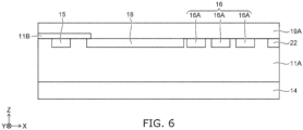
- an n-type layer 11B and a p-type layer 19A are formed on the surface of the n-type layer 11A as shown in FIG. 6 .
- the n-type layer 11B is formed on the entire surface of the n-type layer 11A by epitaxial growth, after which the p-type layer 19A is formed by implanting a p-type impurity into the n-type layer 11B by ion implantation.
- the implantation depth of the p-type impurity implanted in the active region in which the gate electrode 43 will be located is set to be shallower than the implantation depth of the p-type impurity implanted in the region that is further outward than the active region.
- the n-type layer 11B remains on the active region. In the region further outward than the active region, the p-type layer 19A contacts the eighth and sixth layers 18 and 16. The thickness of the p-type layer 19A on the n-type layer 11B remaining in the active region is less than the thickness of the p-type layer 19A in the region further outward than the active region.
- the n-type layer 11A and the n-type layer 11B are included in the first layer 11.
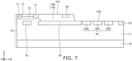
- a portion of the p-type layer 19A is removed to form the first surface 101 and the second surface 102 at the upper surface of the silicon carbide layer 10 as shown in FIG. 7 .
- the second surface 102 that is at a position recessed from the first surface 101 is formed.
- the portion of the p-type layer 19A can be removed by RIE (Reactive Ion Etching).
- the p-type layer 19A that remains on the eighth layer 18 is used to form the ninth layer 19.
- the third layer (the source layer or the emitter layer) 13 is formed in the p-type layer 19A of the active region by implanting an n-type impurity through the first surface 101 by ion implantation.
- the p-type layer 19A that remains under the third layer 13 becomes the second layer (the base layer) 12.
- the seventh layer 17 and the tenth layer 20 that have higher p-type impurity concentrations than the p-type layer 19A are formed by implanting a p-type impurity through the first surface 101.
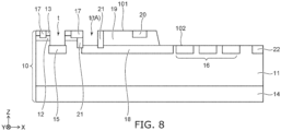
- multiple trenches t that have openings at the first surface 101 are formed in the silicon carbide layer 10.
- the trenches t can be formed by RIE.
- the bottoms of the trenches t reach the fifth layer 15.
- the bottom of an outermost trench tA that is positioned most outward reaches the eighth layer 18.
- the trenches t other than the outermost trench tA are filled with a resist; and ion implantation into the side surface of the outermost trench tA is performed.
- the p-type eleventh layer 21 that has a higher p-type impurity concentration than the second and ninth layers 12 and 19 is formed by implanting a p-type impurity into a region next to the side surface of the outermost trench tA along a direction oblique to the side surface of the outermost trench tA.
- the outermost trench tA also is filled with a resist; and a first layer part 32A that is used to form a portion of the inter-layer insulating film 32 is formed on the entire surface of the first and second surfaces 101 and 102.
- the first layer part 32A can be formed by CVD (Chemical Vapor Deposition).
- the first layer part 32A is patterned to remove the first layer part 32A that is on the first surface 101 so that the first layer part 32A that is on the second surface 102 remains as shown in FIG. 9 .
- the gate insulating film 31 is formed on the side surfaces of the trenches t, the bottom surfaces of the trenches t, the first surface 101, the upper surface of the first layer part 32A, and the interface 105 connecting the first surface 101 and the second surface 102 as shown in FIG. 10 .
- the gate insulating film 31 can be formed by CVD.
- the gate electrode 43 and the field plate 50 are formed.
- a polycrystalline silicon layer is formed by CVD on the gate insulating film 31 to fill the trenches t, after which patterning is performed. After patterning, the polycrystalline silicon layer that remains in the trenches t becomes the gate electrodes 43; and the polycrystalline silicon layer that remains on the first layer part 32A becomes the field plate 50.
- the gate insulating film 31 on the first surface 101 and the gate insulating film 31 on the first layer part 32A are not illustrated and are considered to be portions of the inter-layer insulating film 32.
- a second layer part 32B of the inter-layer insulating film 32 is formed by, for example, CVD on the first surface 101, on the gate electrodes 43, and on the first layer part 32A.
- the field plate 50 is buried in the inter-layer insulating film 32.
- the inter-layer insulating film 32 is thinned by, for example, RIE in the region in which the first electrode 41 will be formed above the first surface 101 as shown in FIG. 13 .
- the flatness of the upper surface of the semiconductor device 1 after forming the first electrode 41 can be improved thereby.
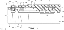
- multiple openings 61 are formed in the inter-layer insulating film 32.
- the openings 61 can be formed by RIE using a resist mask.
- the upper surface of the third layer 13 and the upper surface of the seventh layer 17 are exposed in the openings 61.
- the upper surface of the tenth layer 20 also is exposed in the opening 61.
- the first electrode 41 is formed in the openings 61 and on the inter-layer insulating film 32.
- the second electrode 42 is formed at the back surface of the fourth layer 14.
Landscapes
- Electrodes Of Semiconductors (AREA)
Abstract
A silicon carbide layer includes a first surface, a second surface, a third surface positioned at a side opposite to the first and second surfaces in a first direction, and a side surface. The second surface is at a position recessed further toward the third surface side than the first surface. An inter-layer insulating film is located on the second surface. A thickness of the inter-layer insulating film is greater than a difference in heights in the first direction between the first surface and the second surface. A field plate is located in the inter-layer insulating film. The field plate has a lower resistivity than the inter-layer insulating film.
Description
- Embodiments described herein relate generally to a semiconductor device.
- Power devices that use silicon carbide (SiC) are being developed. SiC devices need a different development approach from silicon devices.
-
-
FIG. 1 is a schematic plan view of a semiconductor device of an embodiment; -
FIG. 2 is an A-A cross-sectional view ofFIG. 1 ; -
FIG. 3 is a schematic cross-sectional view of a semiconductor device of another example of the embodiment; and -
FIG. 4 to FIG. 14 are schematic cross-sectional views showing a method for manufacturing the semiconductor device of the embodiment. - According to one embodiment, a semiconductor device includes a silicon carbide layer including a first surface, a second surface, a third surface positioned at a side opposite to the first and second surfaces in a first direction, and a side surface, the second surface being positioned between the first surface and the side surface in a direction orthogonal to the first direction, the second surface being at a position recessed further toward the third surface side than the first surface; a first electrode located at the first surface; a second electrode located at the third surface; a gate electrode located in the silicon carbide layer between the first surface and the third surface; a gate insulating film located between the gate electrode and the silicon carbide layer; an inter-layer insulating film located on the second surface, a thickness of the inter-layer insulating film being greater than a difference in heights in the first direction between the first surface and the second surface; and a field plate located in the inter-layer insulating film, the field plate having a lower resistivity than the inter-layer insulating film.
- Exemplary embodiments will now be described with reference to the drawings. Similar components in the drawings are marked with like reference numerals. In the description of embodiments described below, a first conductivity type is an n-type, and a second conductivity type is a p-type; however, the first conductivity type may be the p-type, and the second conductivity type may be the n-type.
- As shown in
FIG. 2 , a semiconductor device 1 of the embodiment includes asilicon carbide layer 10. Thesilicon carbide layer 10 includes afirst surface 101, asecond surface 102, athird surface 103, and aside surface 104. Thethird surface 103 is positioned at the side opposite to the first andsecond surfaces first surface 101 and thethird surface 103 with the shortest distance, or a direction connecting thesecond surface 102 and thethird surface 103 with the shortest distance. Two directions orthogonal to the first direction Z are taken as a second direction X and a third direction Y. The second direction X and the third direction Y are orthogonal to each other. - The
second surface 102 is positioned between thefirst surface 101 and theside surface 104 in a direction orthogonal to the first direction Z, and is at a position recessed further toward thethird surface 103 side than thefirst surface 101. In other words, a step is formed between thefirst surface 101 and thesecond surface 102. The step between thefirst surface 101 and thesecond surface 102 is labeled "H" inFIG. 2 . A step H also can be referred to as the height difference in the first direction Z between thefirst surface 101 and thesecond surface 102. - As shown in
FIG. 1 , thesecond surface 102 continuously surrounds thefirst surface 101 when viewed in plan. In the specification, the region where thesecond surface 102 is located is called a termination region TR of the semiconductor device 1. Thesilicon carbide layer 10 is inward of the termination region TR and is formed in a mesa shape. - The semiconductor device 1 further includes a
first electrode 41 located at thefirst surface 101, and asecond electrode 42 located at thethird surface 103. For example, a metal such as aluminum or the like can be used as the material of thefirst electrode 41. For example, a metal such as nickel silicide, titanium, nickel, gold, etc., can be used as the material of thesecond electrode 42. - The semiconductor device 1 further includes a
gate electrode 43 and agate insulating film 31. Thegate electrode 43 has a so-called trench gate structure located in thesilicon carbide layer 10 between thefirst surface 101 and thethird surface 103. Thegate electrode 43 extends in the third direction Y.Multiple gate electrodes 43 are arranged in the second direction X. For example, polycrystalline silicon can be used as the material of thegate electrode 43. - The
gate insulating film 31 is located between thegate electrode 43 and thesilicon carbide layer 10. For example, a silicon oxide film can be used as thegate insulating film 31. - The semiconductor device 1 further includes an inter-layer
insulating film 32 located on thesecond surface 102. A thickness T2 of the inter-layer insulatingfilm 32 on thesecond surface 102 is greater than a thickness T1 of the inter-layer insulatingfilm 32 on thefirst surface 101. The thicknesses T1 and T2 each represent maximum thicknesses in the first direction Z. The thickness T2 of the inter-layer insulatingfilm 32 on thesecond surface 102 is greater than the height difference H in the first direction Z between thefirst surface 101 and thesecond surface 102. The upper surface of the inter-layer insulatingfilm 32 is at a higher position in the first direction Z than the position of thefirst surface 101. The inter-layerinsulating film 32 also is located between thefirst surface 101 and thefirst electrode 41. The inter-layerinsulating film 32 also is located between thefirst electrode 41 and the upper surface of thegate insulating film 31. The inter-layerinsulating film 32 covers aninterface 105 between thefirst surface 101 and thesecond surface 102. For example, a silicon oxide film can be used as the inter-layerinsulating film 32. - The semiconductor device 1 further includes a
field plate 50 located in the inter-layerinsulating film 32 on thesecond surface 102. The inter-layerinsulating film 32 covers an upper surface, lower surface, and side surface of thefield plate 50. - As shown in
FIG. 1 , thefield plates 50 are formed in multiple ring shapes when viewed in plan, and continuously surround thefirst surface 101. - The resistivity of the
field plate 50 is less than the resistivity of the inter-layer insulatingfilm 32. For example, polycrystalline silicon can be used as the material of thefield plate 50. For example, thefield plate 50 is electrically floating. In such a case, the potential of thefield plate 50 is set to a potential between the potential of thefirst electrode 41 and the potential of thesecond electrode 42 in a state in which a voltage is applied to the first andsecond electrodes field plate 50 may be electrically connected with thefirst electrode 41. - The semiconductor device 1 can further include an insulating
protective film 33. Theprotective film 33 covers thefirst electrode 41 and the inter-layerinsulating film 32. For example, a resin such as polyimide or the like can be used as theprotective film 33. - The silicon carbide layer includes an n-type
first layer 11, a p-typesecond layer 12, and an n-typethird layer 13. For example, the semiconductor device 1 has a MOSFET (Metal-Oxide-Semiconductor Field Effect Transistor) or IGBT (Insulated Gate Bipolar Transistor) structure. Thefirst layer 11 functions as a drift layer of a MOSFET or an IGBT. Thesecond layer 12 functions as a base layer of the MOSFET or IGBT. Thethird layer 13 functions as a source layer of the MOSFET, or an emitter layer of the IGBT. - The
first layer 11 is provided continuously between thefirst surface 101 and thethird surface 103 and between thesecond surface 102 and thethird surface 103. Thesecond layer 12 is located on thefirst layer 11 and faces the side surface of thegate electrode 43 via the gateinsulating film 31. Thethird layer 13 is located on thesecond layer 12 and is electrically connected with thefirst electrode 41. The n-type impurity concentration of thethird layer 13 is greater than the n-type impurity concentration of thefirst layer 11. - The
silicon carbide layer 10 further includes afourth layer 14 located between thefirst layer 11 and thesecond electrode 42. Thefourth layer 14 is electrically connected with thesecond electrode 42. In a MOSFET, thefourth layer 14 functions as an n-type drain layer. In such a case, the n-type impurity concentration of thefourth layer 14 is greater than the n-type impurity concentration of thefirst layer 11. In an IGBT, thefourth layer 14 functions as a p-type collector layer. In such a case, the p-type impurity concentration of thefourth layer 14 is greater than the p-type impurity concentration of thesecond layer 12. - The
silicon carbide layer 10 further includes a p-typeseventh layer 17 that is located on thesecond layer 12 and contacts thefirst electrode 41. The p-type impurity concentration of theseventh layer 17 is greater than the p-type impurity concentration of thesecond layer 12. Thesecond layer 12 is electrically connected with thefirst electrode 41 via theseventh layer 17. - In the on-operation of the semiconductor device 1, a potential that is not less than a threshold is applied to the
gate electrode 43; and an inversion layer (an n-type channel) is formed in the region of thesecond layer 12 facing the side surface of thegate electrode 43. A potential that is lower than that of thesecond electrode 42 is applied to thefirst electrode 41; and a potential that is higher than that of thefirst electrode 41 is applied to thesecond electrode 42. A current flows between thefirst electrode 41 and thesecond electrode 42 via thethird layer 13, the n-type channel, thefirst layer 11, and thefourth layer 14 in this state. - When the potential of the
gate electrode 43 drops below the threshold, the n-type channel is cut off, and the semiconductor device 1 is switched to the off-state. In the off-state, depletion layers spread through thefirst layer 11 from the p-n junctions between the n-type first layer 11 (the drift layer) and the p-type layers contacting thefirst layer 11 in thesilicon carbide layer 10; and the breakdown voltage of the semiconductor device 1 is maintained. - In a trench gate structure, the electric field easily concentrates at the bottom portion of the
gate electrode 43. Also, because the dielectric breakdown electric field of the SiOz included in thegate insulating film 31 is less than the dielectric breakdown electric field of silicon carbide (SiC), there is a risk that breakdown of thegate insulating film 31 may occur before breakdown of the SiC. Therefore, according to the embodiment, thesilicon carbide layer 10 further includes a p-typefifth layer 15. Thefifth layer 15 is positioned under thegate electrode 43 in thefirst layer 11 and contacts thegate insulating film 31 located at the bottom surface of thegate electrode 43. Thefifth layer 15 is electrically connected with thefirst electrode 41. The p-type impurity concentration of thefifth layer 15 is greater than the p-type impurity concentration of thesecond layer 12. Thefifth layer 15 can relax the electric field concentration at thegate insulating film 31 located at the bottom surface of thegate electrode 43, thereby suppressing breakdown of thegate insulating film 31. - Because the depletion layer also spreads easily in the termination region TR, it is favorable to provide a p-type layer in the termination region TR at a position that is the same height as the
fifth layer 15. According to the embodiment, thesilicon carbide layer 10 further includes a p-type sixth layer 16. Thesixth layer 16 is positioned under thesecond surface 102 in thefirst layer 11 and positioned at the same height as thefifth layer 15 in the first direction Z. The same height means that thesixth layer 16 is positioned so that the range in which thefifth layer 15 is formed in the first direction Z would pass through at least a portion of thesixth layer 16 if extended along the second direction X (or the third direction Y). The p-type impurity concentration of thesixth layer 16 is greater than the p-type impurity concentration of thesecond layer 12. Thesixth layer 16 is electrically connected with thefirst electrode 41. - In the example shown in
FIG. 2 , thesixth layer 16 includes multiple guard ring layers 16A. Theguard ring layer 16A continuously surrounds a region further inward than thesecond surface 102. - A p-
type sixth layer 16B shown inFIG. 3 may be located in the termination region TR at a position that is at the same height as thefifth layer 15. For example, thesixth layer 16B is positioned under thesecond surface 102 in thefirst layer 11 of the termination region TR and is continuous with a p-typeeighth layer 18 described below. The p-type impurity concentration of thesixth layer 16B is greater than the p-type impurity concentration of thesecond layer 12. Thesixth layer 16B is electrically connected with thefirst electrode 41. - The
sixth layer 16B has a so-called RESURF (REduced Surface Field) structure. Thesixth layer 16B has a p-type impurity concentration gradient in which the p-type impurity concentration proximate to theside surface 104 is less than the p-type impurity concentration proximate to thegate electrode 43. The p-type impurity concentration of thesixth layer 16B gradually decreases from theeighth layer 18 side toward theside surface 104. - Impurities thermally diffuse less easily in SiC than in Si. Therefore, according to the embodiment, by removing a portion of the upper surface side of the
silicon carbide layer 10 as described below, thesixth layer 16 can be distributed in the termination region TR in a range from the same depth as thefifth layer 15 to thesecond surface 102 which is the surface of thesilicon carbide layer 10. - A thick
inter-layer insulating film 32 can be formed by forming the inter-layer insulatingfilm 32 to fill the space on thesecond surface 102 formed by removing the portion of the upper surface side of thesilicon carbide layer 10. The thickinter-layer insulating film 32 can suppress the penetration of moisture from the outside and improve the moisture resistance. For example, structural abnormalities such as oxidization of thefirst electrode 41 due to moisture reacting with the metal of thefirst electrode 41, alteration of theprotective film 33 due to such a structural abnormality, etc., can be suppressed. As a result, the reliability of the semiconductor device 1 can be increased. - Because the thickness of the inter-layer insulating
film 32 is increased by utilizing the space on thesecond surface 102, the height of the entire semiconductor device 1 can be made uniform. The flatness is increased thereby, and the mechanical strength also can be increased. - The
field plate 50 also is provided by utilizing the space on thesecond surface 102. Thefield plate 50 makes it easier for the depletion layer to spread in thesilicon carbide layer 10 of the termination region TR. Local electric field concentration in the termination region TR can be suppressed thereby, and breakdown voltage fluctuation can be suppressed. As a result, the reliability of the semiconductor device 1 can be increased. Thefield plate 50 makes it easier for the depletion layer to spread even when there is much charge in theinter-layer insulating film 32 and at the interface between the inter-layer insulatingfilm 32 and thesecond surface 102 and the extension of the depletion layer due to thesixth layer 16 alone is insufficient. - It is favorable for the
field plate 50 to be positioned within the range from thesecond surface 102 to the height of the first surface 101 (within the range of the step H). In other words, in the first direction Z, it is favorable for the position of the upper surface of thefield plate 50 to be at a position that is at the same or lower height as the position of thefirst surface 101. Because such afield plate 50 is proximate to the interface (the second surface 102) between thesilicon carbide layer 10 and the inter-layer insulatingfilm 32, the effects of thefield plate 50 on the interface can be increased, and the breakdown voltage fluctuation due to effects of the interface charge can be suppressed. Also, because the flatness of the upper surface of the semiconductor device 1 can be better than when the upper surface of thefield plate 50 is at a higher position than the height of thefirst surface 101, process defects can be suppressed, and the mechanical strength can be increased. - It is favorable for the
silicon carbide layer 10 to include the p-typeeighth layer 18 between thefifth layer 15 and thesixth layer 16 at a position that is at the same height as the fifth andsixth layers silicon carbide layer 10 in which thegate electrode 43 is located (the active region in which the current mainly flows in the on-state); and local electric field concentration can be suppressed. The p-type impurity concentration of theeighth layer 18 is greater than the p-type impurity concentration of thesecond layer 12. - A p-type
ninth layer 19 is located on theeighth layer 18. The upper surface of theninth layer 19 is included in thefirst surface 101. A p-type tenth layer 20 is located in theninth layer 19. The p-type impurity concentration of theninth layer 19 is less than the p-type impurity concentration of theeighth layer 18 and the p-type impurity concentration of thetenth layer 20. The p-type impurity concentration of thetenth layer 20 is greater than the p-type impurity concentration of theeighth layer 18. Thetenth layer 20 contacts thefirst electrode 41. Theninth layer 19 is electrically connected with thefirst electrode 41 via thetenth layer 20. - Among the
multiple gate electrodes 43, anoutermost gate electrode 43A that is positioned most proximate to the termination region TR is a dummy electrode that does not function as a gate electrode causing the current to flow in the path described above in the on-operation. Thegate insulating film 31 that is located at the side surface of theoutermost gate electrode 43A contacts the p-typeseventh layer 17 and a p-typeeleventh layer 21. Thegate insulating film 31 that is located at the bottom surface of theoutermost gate electrode 43A contacts theeighth layer 18. The lower end portion of theeleventh layer 21 contacts theeighth layer 18. Theeighth layer 18 is electrically connected with thefirst electrode 41 via the seventh andeleventh layers eleventh layer 21 is less than the p-type impurity concentration of theseventh layer 17 and greater than the p-type impurity concentration of theeighth layer 18. - The
silicon carbide layer 10 can further include an n-typetwelfth layer 22. Thetwelfth layer 22 is positioned at the corner portion between thesecond surface 102 and theside surface 104 on thefirst layer 11 of the termination region TR. Thetwelfth layer 22 is positioned to be separated from thesixth layer 16 in the second and third directions X and Y and is provided in a ring shape along the outer edge of the semiconductor device 1. The n-type impurity concentration of thetwelfth layer 22 is greater than the n-type impurity concentration of thefirst layer 11. The same potential as thesecond electrode 42 is applied to thetwelfth layer 22. Thetwelfth layer 22 functions as a field stop layer that suppresses excessive spreading of the depletion layer so that the depletion layer does not reach theside surface 104. The leakage current of theside surface 104 can be suppressed thereby. Thetwelfth layer 22 is positioned at the same height as thesixth layer 16 in the first direction Z. The depletion layer that spreads from the p-n junction between thesixth layer 16 and thefirst layer 11 can be easily stopped thereby. - A method for manufacturing the semiconductor device 1 according to the embodiment will now be described with reference to
FIGS. 4 to 14 . - As shown in
FIG. 4 , an n-type layer 11A is formed on thefourth layer 14 that is prepared as, for example, a SiC substrate. The n-type layer 11A is epitaxially grown on the fourth layer 14 (the SiC substrate). - As shown in
FIG. 5 , thefifth layer 15, theeighth layer 18, and thesixth layer 16 are formed in the surface of the n-type layer 11A by, for example, implanting a p-type impurity into the surface of the n-type layer 11A by ion implantation. For example, aluminum can be used as the p-type impurity. Also, thetwelfth layer 22 is formed by implanting an n-type impurity into the surface of the n-type layer 11A. For example, nitrogen or phosphorus can be used as the n-type impurity. - After forming the
fifth layer 15, theeighth layer 18, thesixth layer 16, and thetwelfth layer 22, an n-type layer 11B and a p-type layer 19A are formed on the surface of the n-type layer 11A as shown inFIG. 6 . First, the n-type layer 11B is formed on the entire surface of the n-type layer 11A by epitaxial growth, after which the p-type layer 19A is formed by implanting a p-type impurity into the n-type layer 11B by ion implantation. The implantation depth of the p-type impurity implanted in the active region in which thegate electrode 43 will be located is set to be shallower than the implantation depth of the p-type impurity implanted in the region that is further outward than the active region. The n-type layer 11B remains on the active region. In the region further outward than the active region, the p-type layer 19A contacts the eighth andsixth layers type layer 19A on the n-type layer 11B remaining in the active region is less than the thickness of the p-type layer 19A in the region further outward than the active region. The n-type layer 11A and the n-type layer 11B are included in thefirst layer 11. - After forming the p-
type layer 19A, a portion of the p-type layer 19A is removed to form thefirst surface 101 and thesecond surface 102 at the upper surface of thesilicon carbide layer 10 as shown inFIG. 7 . By removing the portion of the p-type layer 19A, thesecond surface 102 that is at a position recessed from thefirst surface 101 is formed. For example, the portion of the p-type layer 19A can be removed by RIE (Reactive Ion Etching). The p-type layer 19A that remains on theeighth layer 18 is used to form theninth layer 19. - The third layer (the source layer or the emitter layer) 13 is formed in the p-
type layer 19A of the active region by implanting an n-type impurity through thefirst surface 101 by ion implantation. The p-type layer 19A that remains under thethird layer 13 becomes the second layer (the base layer) 12. Also, theseventh layer 17 and thetenth layer 20 that have higher p-type impurity concentrations than the p-type layer 19A are formed by implanting a p-type impurity through thefirst surface 101. - Subsequently, as shown in
FIG. 8 , multiple trenches t that have openings at thefirst surface 101 are formed in thesilicon carbide layer 10. For example, the trenches t can be formed by RIE. The bottoms of the trenches t reach thefifth layer 15. The bottom of an outermost trench tA that is positioned most outward reaches theeighth layer 18. - After forming the trenches t, the trenches t other than the outermost trench tA are filled with a resist; and ion implantation into the side surface of the outermost trench tA is performed. The p-type
eleventh layer 21 that has a higher p-type impurity concentration than the second andninth layers - Subsequently, the outermost trench tA also is filled with a resist; and a
first layer part 32A that is used to form a portion of the inter-layer insulatingfilm 32 is formed on the entire surface of the first andsecond surfaces first layer part 32A can be formed by CVD (Chemical Vapor Deposition). Thefirst layer part 32A is patterned to remove thefirst layer part 32A that is on thefirst surface 101 so that thefirst layer part 32A that is on thesecond surface 102 remains as shown inFIG. 9 . - Subsequently, the resist in the trenches t is removed, and the
gate insulating film 31 is formed on the side surfaces of the trenches t, the bottom surfaces of the trenches t, thefirst surface 101, the upper surface of thefirst layer part 32A, and theinterface 105 connecting thefirst surface 101 and thesecond surface 102 as shown inFIG. 10 . For example, thegate insulating film 31 can be formed by CVD. - Subsequently, as shown in
FIG. 11 , thegate electrode 43 and thefield plate 50 are formed. For example, a polycrystalline silicon layer is formed by CVD on thegate insulating film 31 to fill the trenches t, after which patterning is performed. After patterning, the polycrystalline silicon layer that remains in the trenches t becomes thegate electrodes 43; and the polycrystalline silicon layer that remains on thefirst layer part 32A becomes thefield plate 50. - In subsequent drawings, the
gate insulating film 31 on thefirst surface 101 and thegate insulating film 31 on thefirst layer part 32A are not illustrated and are considered to be portions of the inter-layer insulatingfilm 32. - Subsequently, as shown in
FIG. 12 , asecond layer part 32B of the inter-layer insulatingfilm 32 is formed by, for example, CVD on thefirst surface 101, on thegate electrodes 43, and on thefirst layer part 32A. Thefield plate 50 is buried in theinter-layer insulating film 32. - After forming the inter-layer insulating
film 32, the inter-layer insulatingfilm 32 is thinned by, for example, RIE in the region in which thefirst electrode 41 will be formed above thefirst surface 101 as shown inFIG. 13 . The flatness of the upper surface of the semiconductor device 1 after forming thefirst electrode 41 can be improved thereby. - Subsequently, as shown in
FIG. 14 ,multiple openings 61 are formed in theinter-layer insulating film 32. For example, theopenings 61 can be formed by RIE using a resist mask. The upper surface of thethird layer 13 and the upper surface of theseventh layer 17 are exposed in theopenings 61. The upper surface of thetenth layer 20 also is exposed in theopening 61. - As shown in
FIG. 2 , thefirst electrode 41 is formed in theopenings 61 and on theinter-layer insulating film 32. Thesecond electrode 42 is formed at the back surface of thefourth layer 14. - While certain embodiments have been described, these embodiments have been presented by way of example only, and are not intended to limit the scope of the inventions. Indeed, the novel embodiments described herein may be embodied in a variety of other forms; furthermore, various omissions, substitutions and changes in the form of the embodiments described herein may be made without departing from the spirit of the inventions. The accompanying claims and their equivalents are intended to cover such forms or modification as would fall within the scope and spirit of the inventions.
- It is explicitly stated that all features disclosed in the description and/or the claims are intended to be disclosed separately and independently from each other for the purpose of original disclosure as well as for the purpose of restricting the claimed invention independent of the composition of the features in the embodiments and/or the claims. It is explicitly stated that all value ranges or indications of groups of entities disclose every possible intermediate value or intermediate entity for the purpose of original disclosure as well as for the purpose of restricting the claimed invention, in particular as limits of value ranges.
Claims (17)
- A semiconductor device, comprising:a silicon carbide layer includinga first surface,a second surface,a third surface positioned at a side opposite to the first and second surfaces in a first direction, anda side surface, the second surface being positioned between the first surface and the side surface in a direction orthogonal to the first direction, the second surface being at a position recessed further toward the third surface side than the first surface;a first electrode located at the first surface;a second electrode located at the third surface;a gate electrode located in the silicon carbide layer between the first surface and the third surface;a gate insulating film located between the gate electrode and the silicon carbide layer;an inter-layer insulating film located on the second surface, a thickness of the inter-layer insulating film being greater than a difference in heights in the first direction between the first surface and the second surface; anda field plate located in the inter-layer insulating film, the field plate having a lower resistivity than the inter-layer insulating film.
- The device according to claim 1, wherein
the field plate is positioned within a range from the second surface to a height in the first direction of the first surface. - The device according to claim 1 or 2, wherein
the silicon carbide layer includes:a first layer provided continuously between the first surface and the third surface and between the second surface and the third surface, the first layer being of a first conductivity type;a second layer located on the first layer, the second layer facing a side surface of the gate electrode via the gate insulating film, the second layer being of a second conductivity type;a third layer located on the second layer, the third layer being of the first conductivity type and having a higher first-conductivity-type impurity concentration than the first layer, the third layer being electrically connected with the first electrode;a fourth layer located between the first layer and the second electrode, the fourth layer being electrically connected with the second electrode; anda fifth layer positioned under the gate electrode in the first layer, the fifth layer contacting the gate insulating film located at a bottom surface of the gate electrode, the fifth layer being of the second conductivity type. - The device according to claim 3, whereinthe silicon carbide layer further includes a sixth layer positioned under the second surface in the first layer,the sixth layer is positioned at a same height as the fifth layer in the first direction, andthe sixth layer is of the second conductivity type.
- The device according to claim 4, wherein
the sixth layer includes a plurality of guard ring layers. - The device according to claim 4, wherein
the sixth layer has a second-conductivity-type impurity concentration gradient in which a second-conductivity-type impurity concentration of the sixth layer proximate to the side surface is less than the second-conductivity-type impurity concentration of the sixth layer proximate to the gate electrode. - The device according to any of the preceding claims, wherein
the second surface continuously surrounds the first surface. - The device according to any of the preceding claims, wherein
a thickness of the inter-layer insulating film on the second surface is greater than a thickness of the inter-layer insulating film on the first surface. - The device according to any of the preceding claims, wherein
the inter-layer insulating film covers an interface between the first surface and the second surface. - The device according to any of the preceding claims, wherein
the field plate is formed in a plurality of ring shapes. - The device according to any of claims 1-10, wherein
the field plate is electrically floating. - The device according to any of claims 1-10, wherein
the field plate is electrically connected with the first electrode. - The device according to claim 3, 4, 5, or 6, wherein
the fifth layer is electrically connected with the first electrode. - The device according to claim 3, 4, 5, 6 or 13, wherein
a second-conductivity-type impurity concentration of the fifth layer is greater than a second-conductivity-type impurity concentration of the second layer. - The device according to claim 4, 5, or 6, wherein
a second-conductivity-type impurity concentration of the sixth layer is greater than a second-conductivity-type impurity concentration of the second layer. - The device according to claim 4, 5, 6, or 15, wherein
the sixth layer is electrically connected with the first electrode. - The device according to claim 3, 4, 5, 6, 13, or 14, whereinthe silicon carbide layer further includes a field stop layer positioned on the first layer at a corner portion between the second surface and the side surface,the field stop layer is located in a ring shape along an outer edge of the device,the field stop layer is of the first conductivity type, anda first-conductivity-type impurity concentration of the field stop layer is greater than the first-conductivity-type impurity concentration of the first layer.
Applications Claiming Priority (1)
| Application Number | Priority Date | Filing Date | Title |
|---|---|---|---|
| JP2023043325A JP2024132527A (en) | 2023-03-17 | 2023-03-17 | Semiconductor Device |
Publications (1)
| Publication Number | Publication Date |
|---|---|
| EP4432364A1 true EP4432364A1 (en) | 2024-09-18 |
Family
ID=87762959
Family Applications (1)
| Application Number | Title | Priority Date | Filing Date |
|---|---|---|---|
| EP23192622.1A Pending EP4432364A1 (en) | 2023-03-17 | 2023-08-22 | Semiconductor device |
Country Status (4)
| Country | Link |
|---|---|
| US (1) | US20240313108A1 (en) |
| EP (1) | EP4432364A1 (en) |
| JP (1) | JP2024132527A (en) |
| CN (1) | CN118676189A (en) |
Citations (4)
| Publication number | Priority date | Publication date | Assignee | Title |
|---|---|---|---|---|
| US20140077261A1 (en) * | 2012-09-20 | 2014-03-20 | Kabushiki Kaisha Toshiba | Power semiconductor device and method of manufacturing power semiconductor device |
| US20160035840A1 (en) * | 2014-08-04 | 2016-02-04 | Kabushiki Kaisha Toshiba | Semiconductor device |
| US20170301788A1 (en) * | 2014-09-26 | 2017-10-19 | Mitsubishi Electric Corporation | Semiconductor device |
| US20220320268A1 (en) * | 2021-03-30 | 2022-10-06 | Fuji Electric Co., Ltd. | Semiconductor device |
Family Cites Families (3)
| Publication number | Priority date | Publication date | Assignee | Title |
|---|---|---|---|---|
| JP7257927B2 (en) * | 2019-09-19 | 2023-04-14 | 三菱電機株式会社 | semiconductor equipment |
| JP7472477B2 (en) * | 2019-12-02 | 2024-04-23 | 富士電機株式会社 | METHOD FOR MANUFACTURING SILICON CARBIDE SEMICONDUCTOR DEVICE AND METHOD FOR MANUFACTURING SILICON CARBIDE SUBSTRATE |
| KR102417145B1 (en) * | 2020-12-11 | 2022-07-05 | 현대모비스 주식회사 | Power semiconductor device |
-
2023
- 2023-03-17 JP JP2023043325A patent/JP2024132527A/en active Pending
- 2023-06-19 CN CN202310723855.6A patent/CN118676189A/en active Pending
- 2023-08-22 EP EP23192622.1A patent/EP4432364A1/en active Pending
- 2023-08-25 US US18/456,071 patent/US20240313108A1/en active Pending
Patent Citations (4)
| Publication number | Priority date | Publication date | Assignee | Title |
|---|---|---|---|---|
| US20140077261A1 (en) * | 2012-09-20 | 2014-03-20 | Kabushiki Kaisha Toshiba | Power semiconductor device and method of manufacturing power semiconductor device |
| US20160035840A1 (en) * | 2014-08-04 | 2016-02-04 | Kabushiki Kaisha Toshiba | Semiconductor device |
| US20170301788A1 (en) * | 2014-09-26 | 2017-10-19 | Mitsubishi Electric Corporation | Semiconductor device |
| US20220320268A1 (en) * | 2021-03-30 | 2022-10-06 | Fuji Electric Co., Ltd. | Semiconductor device |
Also Published As
| Publication number | Publication date |
|---|---|
| US20240313108A1 (en) | 2024-09-19 |
| JP2024132527A (en) | 2024-10-01 |
| CN118676189A (en) | 2024-09-20 |
Similar Documents
| Publication | Publication Date | Title |
|---|---|---|
| US20240347586A1 (en) | Semiconductor device | |
| JP7724284B2 (en) | Trench-type power devices with improved reliability and continuity | |
| US9059284B2 (en) | Semiconductor device | |
| US11469318B2 (en) | Superjunction semiconductor device having parallel PN structure with column structure and method of manufacturing the same | |
| US11139376B2 (en) | Silicon carbide semiconductor device and method of manufacturing silicon carbide semiconductor device | |
| US8269272B2 (en) | Semiconductor device and method for manufacturing the same | |
| US12009389B2 (en) | Edge termination for power semiconductor devices and related fabrication methods | |
| US9825164B2 (en) | Silicon carbide semiconductor device and manufacturing method for same | |
| JP7643621B2 (en) | Semiconductor Device | |
| US10777678B2 (en) | Semiconductor device | |
| CN107078159A (en) | Semiconductor device | |
| US20230246102A1 (en) | Superjunction semiconductor device | |
| US20110284923A1 (en) | Semiconductor device and manufacturing method of the same | |
| EP2421047A1 (en) | Semiconductor device and method for manufacturing same | |
| US11569376B2 (en) | Silicon carbide semiconductor device and method of manufacturing silicon carbide semiconductor device | |
| US20210320171A1 (en) | Superjunction semiconductor device and method of manufacturing superjunction semiconductor device | |
| US20230275122A1 (en) | Silicon carbide semiconductor device | |
| US20230290817A1 (en) | Silicon carbide semiconductor device | |
| US20240387725A1 (en) | Silicon carbide semiconductor device | |
| US12520551B2 (en) | Silicon carbide semiconductor device and method of manufacturing silicon carbide semiconductor device | |
| US20240313108A1 (en) | Semiconductor device | |
| CN115411111A (en) | Semiconductor device and method for manufacturing the same | |
| US20250098234A1 (en) | Semiconductor device | |
| US20250248065A1 (en) | Semiconductor device and method for manufacturing the same | |
| JP7613604B2 (en) | Silicon carbide semiconductor device |
Legal Events
| Date | Code | Title | Description |
|---|---|---|---|
| PUAI | Public reference made under article 153(3) epc to a published international application that has entered the european phase |
Free format text: ORIGINAL CODE: 0009012 |
|
| STAA | Information on the status of an ep patent application or granted ep patent |
Free format text: STATUS: REQUEST FOR EXAMINATION WAS MADE |
|
| 17P | Request for examination filed |
Effective date: 20230822 |
|
| AK | Designated contracting states |
Kind code of ref document: A1 Designated state(s): AL AT BE BG CH CY CZ DE DK EE ES FI FR GB GR HR HU IE IS IT LI LT LU LV MC ME MK MT NL NO PL PT RO RS SE SI SK SM TR |