EP4432353A1 - Led display pixel element and display device comprising same - Google Patents
Led display pixel element and display device comprising same Download PDFInfo
- Publication number
- EP4432353A1 EP4432353A1 EP22893167.1A EP22893167A EP4432353A1 EP 4432353 A1 EP4432353 A1 EP 4432353A1 EP 22893167 A EP22893167 A EP 22893167A EP 4432353 A1 EP4432353 A1 EP 4432353A1
- Authority
- EP
- European Patent Office
- Prior art keywords
- pads
- leds
- disposed
- layer
- led
- Prior art date
- Legal status (The legal status is an assumption and is not a legal conclusion. Google has not performed a legal analysis and makes no representation as to the accuracy of the status listed.)
- Pending
Links
Images














Classifications
-
- H—ELECTRICITY
- H10—SEMICONDUCTOR DEVICES; ELECTRIC SOLID-STATE DEVICES NOT OTHERWISE PROVIDED FOR
- H10H—INORGANIC LIGHT-EMITTING SEMICONDUCTOR DEVICES HAVING POTENTIAL BARRIERS
- H10H29/00—Integrated devices, or assemblies of multiple devices, comprising at least one light-emitting semiconductor element covered by group H10H20/00
- H10H29/10—Integrated devices comprising at least one light-emitting semiconductor component covered by group H10H20/00
- H10H29/14—Integrated devices comprising at least one light-emitting semiconductor component covered by group H10H20/00 comprising multiple light-emitting semiconductor components
- H10H29/142—Two-dimensional arrangements, e.g. asymmetric LED layout
-
- H—ELECTRICITY
- H10—SEMICONDUCTOR DEVICES; ELECTRIC SOLID-STATE DEVICES NOT OTHERWISE PROVIDED FOR
- H10H—INORGANIC LIGHT-EMITTING SEMICONDUCTOR DEVICES HAVING POTENTIAL BARRIERS
- H10H29/00—Integrated devices, or assemblies of multiple devices, comprising at least one light-emitting semiconductor element covered by group H10H20/00
- H10H29/30—Active-matrix LED displays
- H10H29/34—Active-matrix LED displays characterised by the geometry or arrangement of subpixels within a pixel, e.g. relative disposition of the RGB subpixels
-
- H—ELECTRICITY
- H10—SEMICONDUCTOR DEVICES; ELECTRIC SOLID-STATE DEVICES NOT OTHERWISE PROVIDED FOR
- H10W—GENERIC PACKAGES, INTERCONNECTIONS, CONNECTORS OR OTHER CONSTRUCTIONAL DETAILS OF DEVICES COVERED BY CLASS H10
- H10W90/00—Package configurations
-
- H—ELECTRICITY
- H10—SEMICONDUCTOR DEVICES; ELECTRIC SOLID-STATE DEVICES NOT OTHERWISE PROVIDED FOR
- H10H—INORGANIC LIGHT-EMITTING SEMICONDUCTOR DEVICES HAVING POTENTIAL BARRIERS
- H10H20/00—Individual inorganic light-emitting semiconductor devices having potential barriers, e.g. light-emitting diodes [LED]
- H10H20/80—Constructional details
- H10H20/85—Packages
- H10H20/857—Interconnections, e.g. lead-frames, bond wires or solder balls
-
- H—ELECTRICITY
- H10—SEMICONDUCTOR DEVICES; ELECTRIC SOLID-STATE DEVICES NOT OTHERWISE PROVIDED FOR
- H10W—GENERIC PACKAGES, INTERCONNECTIONS, CONNECTORS OR OTHER CONSTRUCTIONAL DETAILS OF DEVICES COVERED BY CLASS H10
- H10W72/00—Interconnections or connectors in packages
- H10W72/071—Connecting or disconnecting
- H10W72/073—Connecting or disconnecting of die-attach connectors
- H10W72/07351—Connecting or disconnecting of die-attach connectors characterised by changes in properties of the die-attach connectors during connecting
- H10W72/07354—Connecting or disconnecting of die-attach connectors characterised by changes in properties of the die-attach connectors during connecting changes in dispositions
-
- H—ELECTRICITY
- H10—SEMICONDUCTOR DEVICES; ELECTRIC SOLID-STATE DEVICES NOT OTHERWISE PROVIDED FOR
- H10W—GENERIC PACKAGES, INTERCONNECTIONS, CONNECTORS OR OTHER CONSTRUCTIONAL DETAILS OF DEVICES COVERED BY CLASS H10
- H10W72/00—Interconnections or connectors in packages
- H10W72/30—Die-attach connectors
- H10W72/341—Dispositions of die-attach connectors, e.g. layouts
- H10W72/347—Dispositions of multiple die-attach connectors
-
- H—ELECTRICITY
- H10—SEMICONDUCTOR DEVICES; ELECTRIC SOLID-STATE DEVICES NOT OTHERWISE PROVIDED FOR
- H10W—GENERIC PACKAGES, INTERCONNECTIONS, CONNECTORS OR OTHER CONSTRUCTIONAL DETAILS OF DEVICES COVERED BY CLASS H10
- H10W72/00—Interconnections or connectors in packages
- H10W72/30—Die-attach connectors
- H10W72/351—Materials of die-attach connectors
- H10W72/353—Materials of die-attach connectors not comprising solid metals or solid metalloids, e.g. ceramics
-
- H—ELECTRICITY
- H10—SEMICONDUCTOR DEVICES; ELECTRIC SOLID-STATE DEVICES NOT OTHERWISE PROVIDED FOR
- H10W—GENERIC PACKAGES, INTERCONNECTIONS, CONNECTORS OR OTHER CONSTRUCTIONAL DETAILS OF DEVICES COVERED BY CLASS H10
- H10W72/00—Interconnections or connectors in packages
- H10W72/30—Die-attach connectors
- H10W72/351—Materials of die-attach connectors
- H10W72/353—Materials of die-attach connectors not comprising solid metals or solid metalloids, e.g. ceramics
- H10W72/354—Materials of die-attach connectors not comprising solid metals or solid metalloids, e.g. ceramics comprising polymers
-
- H—ELECTRICITY
- H10—SEMICONDUCTOR DEVICES; ELECTRIC SOLID-STATE DEVICES NOT OTHERWISE PROVIDED FOR
- H10W—GENERIC PACKAGES, INTERCONNECTIONS, CONNECTORS OR OTHER CONSTRUCTIONAL DETAILS OF DEVICES COVERED BY CLASS H10
- H10W90/00—Package configurations
- H10W90/20—Configurations of stacked chips
- H10W90/297—Configurations of stacked chips characterised by the through-semiconductor vias [TSVs] in the stacked chips
-
- H—ELECTRICITY
- H10—SEMICONDUCTOR DEVICES; ELECTRIC SOLID-STATE DEVICES NOT OTHERWISE PROVIDED FOR
- H10W—GENERIC PACKAGES, INTERCONNECTIONS, CONNECTORS OR OTHER CONSTRUCTIONAL DETAILS OF DEVICES COVERED BY CLASS H10
- H10W90/00—Package configurations
- H10W90/701—Package configurations characterised by the relative positions of pads or connectors relative to package parts
- H10W90/731—Package configurations characterised by the relative positions of pads or connectors relative to package parts of die-attach connectors
- H10W90/732—Package configurations characterised by the relative positions of pads or connectors relative to package parts of die-attach connectors between stacked chips
Definitions
- the present disclosure relates to a pixel device for an LED display that implements an image using a light emitting diode and a display apparatus having the same.
- Light emitting diodes are inorganic light sources, which are used in various fields such as display apparatuses, automobile lamps, general lighting, and the like.
- the light emitting diodes have advantages such as longer lifespan, lower power consumption, and quicker response, than conventional light sources, and thus, they have been replacing the conventional light sources.
- the conventional light emitting diodes have been generally used as backlight light sources in display apparatuses.
- LED displays that directly realize images using the light emitting diodes have been recently developed.
- the display apparatus displays various colors through mixture of blue, green, and red light.
- the display apparatus includes a plurality of pixels, each of the pixels includes sub-pixels of blue, green, and red light, a color of a certain pixel is determined based on colors of the sub-pixels, and images can be realized through a combination of such pixels.
- An LED display apparatus implements an image by using a very small LED in a micro unit.
- numerous pixel devices are manufactured, and the pixel devices are mounted on a circuit board using pads formed on the pixel devices.
- Each of the pixel devices includes one or more pixels.
- the pixel device may include a pixel in which LEDs are laterally arranged or a pixel in which LEDs are vertically stacked.
- the pixel of a vertically stacked structure is generally manufactured by bonding semiconductor layers grown on different growth substrates using a wafer-wafer bonding technique.
- the pixel device is manufactured by patterning semiconductor layers bonded to one another at a wafer level, forming an electrode structure for electrical connection, and thereafter, dividing the pixel device into individual pixel device units.
- the electrode structure is formed after bonding the semiconductor layers, etching for different materials such as semiconductor layers and insulation layers is required, and since etching is required through several layers, it is difficult to generate a hole having a relatively large aspect ratio. Accordingly, it is difficult to form the electrode structure, and a pixel manufacturing process is complicated.
- the defective pixel device since electrical characteristics or optical characteristics can be measured after the pixel device is completed, whether or not the pixel device is defective can be checked only after the pixel device is completed. When a defective pixel device is identified, the defective pixel device is discarded or repaired. Since blue, green, and red LEDs have a stacked structure, even when a defect occurs in any one of the LEDs, it leads to a defect in the pixel device, resulting in a very low yield of the pixel devices. In addition, even when the defective pixel device is repaired, since a repair process has to be performed after a final pixel device is completed, it is relatively difficult to repair the pixel device. Accordingly, even when repair is possible, the defective pixel device is often discarded instead of repairing it due to drawbacks such as process complexity and cost, and thus, it is difficult to increase a process yield of pixel devices through repair.
- Exemplary embodiments of the present disclosure provide a pixel device having a structure in which LEDs are vertically stacked and having a novel structure that is configured to increase a process yield, and a display apparatus having the same.
- Exemplary embodiments of the present disclosure provide a pixel device that is configured to easily repair defective LEDs during a manufacturing process and a display apparatus having the same.
- Exemplary embodiments of the present disclosure may simplify a manufacturing process and provide a pixel device in which an electrode structure is easily formed and a display apparatus having the same.
- a pixel device includes a first floor including a first LED, and a first lower pad and a first upper pad electrically connected to the first LED; a second floor disposed over the first floor, and including a second LED, and a second lower pad and a second upper pad electrically connected to the second LED; and a third floor disposed over the second floor, and including a third LED, and a third lower pad and a third upper pad electrically connected to the third LED.
- a term "pixel device” refers to a unit device configured to be mounted on a circuit board.
- the pixel device may include one or more pixels.
- the pixel is generally a basic unit constituting an image in a display.
- one pixel may include at least three sub-pixels each emitting a single color.
- a term "pixel" refers to a combination of the sub-pixels, and the sub-pixels are stacked one above another.
- the first LED, the second LED, and the third LED may emit visible light of different colors from one another.
- the first LED may emit blue light
- the second LED may emit green light
- the third LED may emit red light
- the first LED may emit green light
- the second LED may emit blue light
- the third LED may emit red light.
- the first through third lower pads may be electrically connected to one another, and the first through third upper pads may be electrically spaced apart from one another.
- the pixel device may include a lower adhesive layer bonding the first floor and the second floor; and an upper adhesive layer bonding the second floor and the third floor.
- the first through third LEDs may be disposed so as to overlap one another in a vertical direction.
- a pixel is provided by the first through third LEDs overlapping in the vertical direction.
- the first through third LEDs may partially overlap one another.
- the pixel device may further include a light blocking layer surrounding the first LED, the second LED, or the third LED.
- the first floor may further include a first insulation layer covering the first LEDs and a first planarization layer covering the insulation layer, and the first upper pad may be disposed on the first planarization layer. Furthermore, the first lower pad may be disposed between the first insulation layer and the first planarization layer or on the first planarization layer.
- the second floor may further include a second insulation layer covering the second LEDs and a second planarization layer covering the second insulation layer, and the second upper pad may be disposed on the second planarization layer. Furthermore, the second lower pad may be disposed between the second insulation layer and the second planarization layer or on the second planarization layer.
- the third floor may further include a third insulation layer covering the third LEDs and a third planarization layer covering the third insulation layer, and the third upper pad may be disposed on the third planarization layer. Furthermore, the third lower pad may be disposed between the third insulation layer and the third planarization layer or on the third planarization layer.
- the pixel device may further include an upper insulation layer covering the third floor and pixel device pads disposed on the upper insulation layer.
- Each of the pixel device pads may be electrically connected to at least one of the first through third lower pads and the first through third upper pads.
- a plurality of first LEDs, a plurality of second LEDs, and a plurality of third LEDs may be arranged in a matrix of n ⁇ m (n, m is a positive integer) on the first through third floors, respectively, and the number of pixel pad electrodes may be (3n+m).
- the pixel device pads may be electrically connected to at least one of the first through third lower pads and the first through third upper pads through connection vias.
- the connection vias may be spaced apart from the first through third LEDs in a lateral direction.
- the first through third lower pads may be electrically connected to cathodes of the first through third LEDs, respectively, and the first through third upper pads may be electrically connected to anodes of the first through third LEDs, respectively.
- a display apparatus includes a circuit board and a pixel device disposed on the circuit board, in which the pixel device includes a first floor including a first LED, and a first lower pad and a first upper pad electrically connected to the first LED; a second floor disposed over the first floor, and including a second LED, and a second lower pad and a second upper pad electrically connected to the second LED; and a third floor disposed over the second floor, and including a third LED, and a third lower pad and a third upper pad electrically connected to the third LED.
- the pixel device may further include an upper insulation layer disposed on the third floor and pixel device pads disposed on the upper insulation layer, and the pixel device pads may be bonded to the circuit board.
- the pixel device pads may be electrically connected to at least one of the first through third lower pads and the first through third upper pads through connection vias, and the connection vias may be spaced apart from the first through third LEDs in a lateral direction.
- FIG. 1A is a schematic plan view illustrating a display apparatus according to an exemplary embodiment
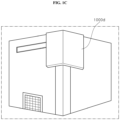
- FIGS. 1B , 1C , and 1D are schematic perspective views illustrating various display apparatuses 1000a, 1000b, 1000c, and 1000d according to an exemplary embodiment.
- a display apparatus 10000 may include a panel substrate 2100 and a plurality of pixel modules 1000.
- the display apparatus 10000 is not particularly limited, but may include a smart watch 1000a, a wearable display apparatus 1000b such as a VR headset or glasses, an AR display apparatus 1000c such as augmented reality glasses, or an indoor or outdoor display apparatus 1000d or 1000e such as a micro LED TV or signage.
- the panel substrate 2100 and the plurality of pixel modules 1000 may be disposed in the display apparatus.
- a gap between pixels in the display apparatus may be very narrow, for example, the gap between pixels may be 0.01 mm or less.
- the display apparatus may implement an image through pixels mounted on a circuit board or a transparent substrate. In some display apparatuses, a distance between the display apparatus and an external receiver (e.g., a user's eyes) that recognizes the display may be 200 mm or less.
- the gap between pixels may be 0.005% to 0.1% of the distance between the external receiver and the display apparatus.
- the display apparatus may transmit an optical signal from a substrate including a curved surface to the external receiver.
- the display apparatus may also be a transparent display apparatus using a transparent substrate.
- the panel substrate 2100 may include a circuit for a passive matrix driving or active matrix driving manner.
- the panel substrate 2100 may include wirings and resistors therein, and, in another exemplary embodiment, the panel substrate 2100 may include wirings, transistors, and capacitors.
- the panel substrate 2100 may also have pads that are capable of being electrically connected to the disposed circuit on an upper surface thereof.
- the plurality of pixel modules 1000 is arranged on the panel substrate 2100.
- Each of the pixel modules 1000 may include a circuit board 1001, and a plurality of pixel devices 100 disposed on the circuit board 1001, and may include a molding member covering the pixel devices 100.
- the plurality of pixel devices 100 may be directly arranged on the panel substrate 2100, and the molding member may cover the pixel devices 100.
- the smart watch 1000a may be 500 to 1500cd/m 2 (or nits) or more, and a brightness thereof may be adjusted according to an external illumination.
- the wearable display apparatus 1000b such as a VR headset or glasses may be 150 to 200 cd/m 2 (or nits), or a viewing angle thereof may be 50 degrees or more.
- the indoor or outdoor display apparatus 1000d or 1000e such as Micro LED TV or signage is preferably 1000 cd/m 2 (or nits) or more, or 80 degrees or more viewing angle, especially for outdoor use, 3000 cd/m 2 (or nits) or more.
- a plurality of panels P1 and P2 is arranged in rows and columns and attached to a frame, and a plurality of micro LED pixels is disposed on the plurality of panels P1 and P2 to supply electricity or signals, and thus, the display apparatus may be turned on or its luminous intensity may be adjusted according to electricity supply or signals.
- the plurality of panels P1 and P2 may be connected to an external power source using respective connectors, or the plurality of panels P1 and P2 may be electrically connected to one another using connectors.
- a pixel device 100 according to an exemplary embodiment will be described in detail with reference to FIGS. 2A , 2B , 2C , 3A , 3B , and 3C .
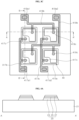
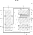
- FIG. 2A is a schematic plan view illustrating the pixel device 100 according to an exemplary embodiment
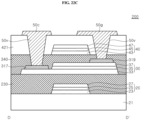
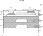
- FIGS. 2B and 2C are schematic cross-sectional views taken along lines A-A' and BB' of FIG. 2A , respectively.
- the pixel device includes a plurality of floors, and each of the floors is shown in FIGS 3A , 3B and 3C .
- a pixel device including pixels arranged in a 2 ⁇ 2 matrix will be described as an example.
- the pixel device 100 may include a substrate 21, light blocking layers 213, 313, and 413, insulation layers 215, 315, and 415, planarization layers 221, 321 and 421, lower and upper adhesive layers 230 and 340, LEDs 20, 30, and 40, first lower pads 217a1 and 217a2, first lower connection lines 217b, and first lower contacts 217c, first upper pads 219a1 and 219a2, first upper connection lines 219b, first upper contacts 219c, second lower pads 317a1 and 317a2, second lower connection lines 317b, second lower contacts 317c, second upper pads 319a1 and 319a2, second upper connection lines 319b, second upper contacts 319c, third lower pads 417a1 and 417a2, third lower connection lines 417b, third lower contacts 417c, third upper pads 419a1 and 419a2, third upper connection lines 419b, third upper contacts 419c, an upper insulation layer 423, connection vias 50
- the pixel device 100 may include first through third floors disposed on the substrate 21, and these floors may be bonded through the adhesive layers 230 and 340, respectively.
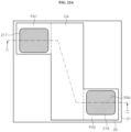
- the first floor includes the LEDs 20, the first lower pads 217a1 and 217a2, the first lower connection lines 217b, the first lower contacts 217c, the first upper pads 219a1 and 219a2, the first upper connection lines 219b, and the first upper contacts 219c
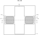
- the second floor includes the LEDs 30, the second lower pads 317a1 and 317a2, the second lower connection lines 317b, the second lower contacts 317c, the second upper pads 319a1 and 319a2, the second upper connection lines 319b, and the second upper contacts 319c
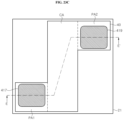
- the third floor includes the LEDs 40, the third lower pads 417a1 and 417a2, the third lower connection lines 417b, the third lower contacts 417c, the third upper pads 419a1 and 419a2, the third upper connection lines 419b, and the third upper contacts 419c.
- the substrate 21 is a transparent substrate that transmits light generated in the pixels 20, 30, and 40, and may include a light-transmissive insulating material. In some exemplary embodiments, the substrate 21 may be translucent or partially transparent so as to transmit only light of a specific wavelength or only a portion of light of a specific wavelength.
- the substrate 21 may include glass, quartz, silicon, an organic polymer, or an organic-inorganic composite material, for example, silicon carbide (SiC), gallium nitride (GaN), indium gallium nitride (InGaN), aluminum gallium nitride (AlGaN), aluminum nitride (AlN), gallium oxide (Ga 2 O 3 ) substrate, and the like.
- the substrate 21 may be omitted.
- the LEDs 20 are arranged on the substrate 21.
- the inventive concepts are not limited thereto.
- one LED 20 may be disposed on the substrate 21, or two or more LEDs 20 may be disposed.
- Each of the LEDs 20 includes a first conductivity type semiconductor layer 23, an active layer 25, and a second conductivity type semiconductor layer 27.
- the active layer 25 may be disposed between the first conductivity type semiconductor layer 23 and the second conductivity type semiconductor layer 27.
- the first conductivity type semiconductor layer 23 may be, for example, an n-type conductivity type semiconductor layer, and the second conductivity type semiconductor layer 27 may be a p-type conductivity type semiconductor layer, and vice versa.
- the LED 20 may include a semiconductor material that emits blue light, such as GaN, InGaN, ZnSe, or the like, without being limited thereto, and may emit red or green light.
- the LED 20 may be patterned such that a portion of the first conductivity type semiconductor layer 23 is exposed through the second conductivity type semiconductor layer 27 and the active layer 25. As shown in FIG. 2C , a portion of an upper surface of the first conductivity type semiconductor layer 23 is exposed. In this embodiment, it is shown that the second conductivity type semiconductor layer 27 and the active layer 25 are partially removed near an edge of the first conductivity type semiconductor layer 23, but the inventive concepts are not limited thereto, and a through hole passing through the second conductivity type semiconductor layer 27 and the active layer 25 may be formed to expose the first conductivity type semiconductor layer 23.
- a light blocking layer 213 is disposed on the substrate 21.
- the light blocking layer 213 surrounds the LEDs 20 and defines a window region 213a through which light is emitted.
- the light blocking layer 20 may be formed of, for example, a black matrix, and may improve a contrast ratio by preventing cross-talk between the LEDs 20, 30, and 40 in the display apparatus 10000.
- the light blocking layer 213 may be omitted.
- the window region 213a through which light is emitted to the outside may be larger than or equal to a lower surface area of the LED 20.
- the LED 20 may be in contact with the light blocking layer 213.
- the insulation layer 215 covers the LEDs 20. Additionally, the insulation layer 215 may cover the light blocking layer 213.
- the insulation layer 215 may be formed of a light-transmitting material.
- the insulation layer 215 may include silicon oxide such as SiO 2 , silicon nitride such as Si 3 N 4 , or silicon oxynitride.
- the insulation layer 215 may be patterned so as to allow electrical connection to the first conductivity type semiconductor layer 23 and the second conductivity type semiconductor layer 27.
- the insulation layer 215 may have openings exposing the first conductivity type semiconductor layer 23 and the second conductivity type semiconductor layer 27.
- a transparent electrode may be formed on the second conductivity type semiconductor layer 27, and in this case, the opening of the insulation layer 215 may expose the transparent electrode.
- the first lower pads 217a1 and 217a2, the first lower connection lines 217b, and the first lower contacts 217c are formed on the insulation layer 215.
- the first lower contacts 217c are electrically connected to the first conductivity type semiconductor layer 23 of the LEDs 20.
- the first lower contact 217c may be connected to the first conductivity type semiconductor layer 23 through the opening of the insulation layer 215. Since the first lower contacts 217c are disposed on the LEDs 20, respectively, the number of first lower contacts 217c is at least equal to the number of the LEDs 20.
- the first lower pads 217a1 and 217a2 may be spaced apart from the LEDs 20 in a lateral direction and disposed on the insulation layer 215. In an embodiment, both of the first lower pads 217a1 and 217a2 are spaced apart from the LEDs 20 and disposed near one side (lower side) of the substrate 21, as shown in FIG. 3A . However, the inventive concepts are not limited thereto, and at least one of the first lower pads 217a1 and 217a2 may be disposed in a region between the LEDs 20. In an embodiment, the first lower pads 217a1 and 217a2 may be disposed at least as many as the number of columns of the LEDs 20. In this embodiment, since the LEDs 20 are disposed in two rows, two first lower pads 217a1 and 217a2 are disposed.
- the first lower connection lines 217b connect the first lower contacts 217c to the first lower pads 217a1 and 217a2. As shown in FIG. 3A , the first lower connection lines 217b may electrically connect the first lower contacts 217c on the LEDs 20 disposed in a same column to a same first lower pad 217a1 or 217a2. That is, one first lower connection line 217b connects the first lower contacts 217c disposed in a first column to the first lower pad 217a1, and another first lower connection line 217b connects the first lower contacts 217c disposed in a second column to the first lower pad 217a2. The first lower connection lines 217b may be provided in a same number as those of the first lower pads 217a1 and 217a2.
- the planarization layer 221 covers the LEDs 20, the insulation layer 215, the first lower pads 217a1 and 217a2, the first lower contacts 217c, and the first lower connection lines 217b.
- the planarization layer 221 may cover a surface morphology formed by the LEDs 20 to provide a flat upper surface.
- the planarization layer 221 may be formed of a light-transmitting insulating material such as polyimide (PI) or epoxy molding compound (EMC).
- the first upper pads 219a1 and 219a2, the first upper connection lines 219b, and the first upper contacts 219c are formed on the planarization layer 221.
- the first upper contacts 219c are electrically connected to the second conductivity type semiconductor layers 27 of the LEDs 20.
- the first upper contact 219c may be electrically connected to the second conductivity type semiconductor layers 27 through the planarization layer 221 and the insulation layer 215. Since the first upper contacts 219c are disposed on the LEDs 20, respectively, the number of first upper contacts 219c is at least equal to the number of the LEDs 20.
- the first upper pads 219a1 and 219a2 may be spaced apart from the LEDs 20 in the lateral direction and disposed on the planarization layer 221. Also, the first upper pads 219a1 and 219a2 are spaced apart from the first lower pads 217a1 and 217a2 in the lateral direction. That is, the first upper pads 219a1 and 219a2 are disposed on the planarization layer 221 so as not to overlap the first lower pads 217a1 and 217a2. In an embodiment, both of the first upper pads 219a1 and 219a2 may be spaced apart from the LEDs 20 and disposed near one side (right side) of the substrate 21, as shown in FIG. 3A .
- the inventive concepts are not limited thereto, and at least one of the first upper pads 219a1 and 219a2 may be disposed in the region between the LEDs 20.
- the first upper pads 217a1 and 217a2 may be disposed at least as many as the number of rows of the LEDs 20. In this embodiment, since the LEDs 20 are disposed in two rows, two first upper pads 219a1 and 219a2 are disposed.
- the first upper connection lines 219b connect the first upper contacts 219c to the first upper pads 219a1 and 219a2. As shown in FIG. 3A , the first upper connection lines 219b may connect the first upper contacts 219c on the LEDs 20 arranged in a same row to a same first upper pad 219a1 or 219a2. That is, one first upper connection line 219b connects the first upper contacts 219c disposed in a first row to the first upper pad 219a1, and another first upper connection line 219b connects the first upper contacts 219c disposed in a second row to the first upper pad 219a2. The first upper connection lines 219b may be provided in a same number as those of the first upper pads 219a1 and 219a2.
- the first lower pads 217a1 and 217a2 are illustrated and described as being disposed between the insulation layer 215 and the planarization layer 221, but the inventive concepts are not limited thereto.
- the first lower pads 217a1 and 217a2, the first lower contacts 217c, and the first lower connection lines 217b may be disposed on the planarization layer 221, and the first lower contacts 217c may be electrically connected to the first conductivity type semiconductor layer 23 through the planarization layer 221 and the insulation layer 215.
- additional pads electrically connected to the first lower pads 217a1 and 217a2 may be provided on the planarization layer 221.
- the second floor may include the LEDs 30, the light blocking layer 313, the insulation layer 315, the second lower contacts 317c, the second lower pads 317a1 and 317a2, the second lower connection lines 317b, the planarization layer 321, the second upper contacts 319c, the second upper pads 319a1 and 319a2, and the second upper connection lines 319b.
- the second floor may be attached to the first floor by the lower adhesive layer 230.
- the lower adhesive layer 230 covers the first upper contacts 219c, the first upper pads 219a1 and 219a2, the first upper connection lines 219b, and the planarization layer 221.
- the lower adhesive layer 230 may include an optically clear adhesive (OCA), which, for example, may include epoxy, polyimide, SU8, spin-on-glass (SOG), benzocyclobutene (BCB), without being limited thereto.
- OCA optically clear adhesive
- the LEDs 30 may be attached to the lower adhesive layer 230. In this embodiment, it is described that four LEDs 30 are arranged, but the inventive concepts are not limited thereto.
- the LEDs 30 may be arranged in a same number as that of the LEDs 20, and may be arranged such that at least a portion of a light emitting region overlaps the LEDs 20.
- Each of the LEDs 30 includes a first conductivity type semiconductor layer 33, an active layer 35, and a second conductivity type semiconductor layer 37.
- the active layer 35 may be disposed between the first conductivity type semiconductor layer 33 and the second conductivity type semiconductor layer 37.
- the first conductivity type semiconductor layer 33 may be, for example, an n-type conductivity type semiconductor layer
- the second conductivity type semiconductor layer 37 may be a p-type conductivity type semiconductor layer, and vice versa.
- the LED 30 may include a semiconductor material that emits green light, such as GaN, InGaN, GaP, AlGaInP, AlGaP, or the like, without being limited thereto, and may emit red or blue light.
- the LED 30 may be patterned such that a portion of the first conductivity type semiconductor layer 33 is exposed through the second conductivity type semiconductor layer 37 and the active layer 35. As shown in FIG. 2C , a portion of an upper surface of the first conductivity type semiconductor layer 33 is exposed. In this embodiment, it is shown that the second conductivity type semiconductor layer 37 and the active layer 35 are partially removed near an edge of the first conductivity type semiconductor layer 33, but the inventive concepts are not limited thereto, and a through hole passing through the second conductivity type semiconductor layer 37 and the active layer 35 may be formed to expose the first conductivity type semiconductor layer 33.
- the light blocking layer 313 is disposed on the lower adhesive layer 230.
- the light blocking layer 313 surrounds the LEDs 30 and defines a window region 313a through which light is emitted.
- the light blocking layer 313 may be formed of, for example, a black matrix, and may improve a contrast ratio by preventing cross-talk between the LEDs 20, 30, and 40 in the display apparatus 10000.
- the light blocking layer 313 may be omitted.
- the window region 313a formed by the light blocking layer 313 may be larger than or equal to a lower surface area of the LED 30.
- the LED 30 may be in contact with the light blocking layer 313.
- the insulation layer 315 covers the LEDs 30.
- the insulation layer 315 may also cover the light blocking layer 313.
- the insulation layer 315 may be formed of a light-transmitting material.
- the insulation layer 315 may include silicon oxide such as SiO 2 , silicon nitride such as Si 3 N 4 , or silicon oxynitride.
- the insulation layer 315 may be patterned so as to allow electrical connection to the first conductivity type semiconductor layer 33 and the second conductivity type semiconductor layer 37.
- the insulation layer 315 may have openings exposing the first conductivity type semiconductor layer 33 and the second conductivity type semiconductor layer 37.
- a transparent electrode may be formed on the second conductivity type semiconductor layer 37, and in this case, the opening of the insulation layer 315 may expose the transparent electrode.
- the second lower pads 317a1 and 317a2, the second lower connection lines 317b, and the second lower contacts 317c are formed on the insulation layer 315.
- the second lower contacts 317c are electrically connected to the first conductivity type semiconductor layer 33 of the LEDs 30.
- the second lower contact 317c may be connected to the first conductivity type semiconductor layer 33 through the opening of the insulation layer 315. Since the second lower contacts 317c are disposed on the LEDs 30, respectively, the number of second lower contacts 317c is at least equal to the number of the LEDs 30.
- the second lower pads 317a1 and 317a2 may be spaced apart from the LEDs 30 in the lateral direction and disposed on the insulation layer 315.
- the second lower pads 317a1 and 317a2 may be disposed so as to overlap the first lower pads 217a1 and 217a2, respectively.
- both of the second lower pads 317a1 and 317a2 may be spaced apart from the LEDs 30 and disposed near one side (lower side) of the substrate 21, as shown in FIG. 3B .
- the inventive concepts are not limited thereto, and at least one of the second lower pads 317a1 and 317a2 may be disposed in a region between the LEDs 30.
- the second lower pads 317a1 and 317a2 may be laterally spaced apart from the first lower pads 217a1 and 217a2 so as to partially overlap or so as not to overlap the first lower pads 217a1 and 217a2.
- the second lower pads 317a1 and 317a2 may be disposed at least as many as the number of columns of the LEDs 30. In this embodiment, since the LEDs 30 are disposed in two rows, two second lower pads 317a1 and 317a2 are disposed.
- the second lower connection lines 317b electrically connect the second lower contacts 317c to the second lower pads 317a1 and 317a2. As shown in FIG. 3A , the second lower connection lines 317b may connect the second lower contacts 317c on the LEDs 30 disposed in a same column to a same second lower pad 317a1 or 317a2. That is, one second lower connection line 317b connects the second lower contacts 317c disposed in a first column to the second lower pad 317a1, and another second lower connection line 317b connects the second lower contacts 317c disposed in a second column to the second lower pad 317a2.
- the second lower connection lines 317b may be provided in a same number as those of the second lower pads 317a1 and 317a2.
- the planarization layer 321 covers the LEDs 30, the insulation layer 315, the second lower pads 317a1 and 317a2, the second lower contacts 317c, and the second lower connection lines 317b.
- the planarization layer 321 may cover a surface morphology formed by the LEDs 30 to provide a flat upper surface.
- the planarization layer 321 may be formed of a light-transmitting insulating material such as polyimide (PI) or epoxy molding compound (EMC).
- the second upper pads 319a1 and 319a2, the second upper connection lines 319b, and the second upper contacts 319c are formed on the planarization layer 321.
- the second upper contacts 319c are electrically connected to the second conductivity type semiconductor layers 37 of the LEDs 30.
- the second upper contact 319c may be electrically connected to the second conductivity type semiconductor layers 37 through the planarization layer 321 and the insulation layer 315. Since the second upper contacts 319c are disposed on the LEDs 30, respectively, the number of second upper contacts 319c is at least equal to the number of the LEDs 30.
- the second upper pads 319a1 and 319a2 may be spaced apart from the LEDs 30 in the lateral direction and disposed on the planarization layer 321. Also, the second upper pads 319a1 and 319a2 are spaced apart from the second lower pads 317a1 and 317a2 in the lateral direction. Furthermore, the second upper pads 319a1 and 319a2 may be spaced apart from the first upper pads 219a1 and 219a2 in the lateral direction. That is, the second upper pads 319a1 and 319a2 may be disposed on the planarization layer 321 so as not to overlap the first lower pads 217a1 and 217a2, the first upper pads 219a1 and 219a2, and the second lower pads 317a1 and 317a2.
- both of the second upper pads 319a1 and 319a2 may be spaced apart from the LEDs 30 and disposed near one side (left side) of the substrate 21, as shown in FIG. 3B .
- the inventive concepts are not limited thereto, and at least one of the second upper pads 319a1 and 319a2 may be disposed in the region between the LEDs 30.
- the second upper pads 317a1 and 317a2 may be disposed at least as many as the number of rows of the LEDs 30. In this embodiment, since the LEDs 30 are disposed in two rows, two second upper pads 319a1 and 319a2 are disposed.
- the second upper connection lines 319b electrically connect the second upper contacts 319c to the second upper pads 319a1 and 319a2. As shown in FIG. 3B , the second upper connection lines 319b may connect the second upper contacts 319c on the LEDs 30 disposed in a same row to a same second upper pad 319a1 or 319a2. That is, one second upper connection line 319b connects the second upper contacts 319c disposed in a first row to the second upper pad 319a1, and another second upper connection line 319b connects the second upper contacts 319c disposed in a second row to the second upper pad 319a2.
- the second upper connection lines 319b may be provided in a same number as those of the second upper pads 319a1 and 319a2.
- the second lower pads 317a1 and 317a2 are illustrated and described as being disposed between the insulation layer 315 and the planarization layer 321, but the inventive concepts are not limited thereto.
- the second lower pads 317a1 and 317a2, the second lower contacts 317c, and the second lower connection lines 317b may be disposed on the planarization layer 321, and the second lower contacts 317c may be electrically connected to the first conductivity type semiconductor layer 33 through the planarization layer 321 and the insulation layer 315.
- additional pads electrically connected to the second lower pads 317a1 and 317a2 may be provided on the planarization layer 321.
- the third floor may include the LEDs 40, the light blocking layer 413, the insulation layer 415, the third lower contacts 417c, the third lower pads 417a1 and 417a2, and the third lower connection lines 417b, the planarization layer 421, the third upper contacts 419c, the third upper pads 419a1 and 419a2, and the third upper connection lines 419b.
- the third floor may be attached to the second floor by the upper adhesive layer 340.
- the upper adhesive layer 340 covers the second upper contacts 319c, the second upper pads 319a1 and 319a2, the second upper connection lines 319b, and the planarization layer 321.
- the upper adhesive layer 340 may include an optically clear adhesive (OCA), for example, epoxy, polyimide, SU8, spin-on-glass (SOG), or benzocyclobutene (BCB), without being limited thereto.
- OCA optically clear adhesive
- OCA optically clear adhesive
- SOG spin-on-glass
- BCB benzocyclobutene
- the LEDs 40 may be attached to the upper adhesive layer 340. In this embodiment, it is described that four LEDs 40 are arranged, but the inventive concepts are not limited thereto.
- the LEDs 30 may be disposed in a same number as that of the LEDs 20 and may be disposed so as to overlap the LEDs 20. One pixel is provided by the LEDs 20, 30, and 40 overlapping one another.
- Each of the LEDs 40 includes a first conductivity type semiconductor layer 43, an active layer 45, and a second conductivity type semiconductor layer 47.
- the active layer 45 may be disposed between the first conductivity type semiconductor layer 43 and the second conductivity type semiconductor layer 47.
- the first conductivity type semiconductor layer 43 may be, for example, an n-type conductivity type semiconductor layer
- the second conductivity type semiconductor layer 47 may be a p-type conductivity type semiconductor layer, and vice versa.
- the LED 40 may include a semiconductor material that emits red light, such as AlGaAs, GaAsP, AlGaInP, and GaP, without being limited thereto, and may emit blue or green light based on a nitride semiconductor.
- the LED 40 may be patterned such that a portion of the first conductivity type semiconductor layer 43 is exposed through the second conductivity type semiconductor layer 47 and the active layer 45. As shown in FIG. 2C , a portion of an upper surface of the first conductivity type semiconductor layer 43 is exposed. In this embodiment, it is shown that the second conductivity type semiconductor layer 47 and the active layer 45 are partially removed near an edge of the first conductivity type semiconductor layer 43, but the inventive concepts are not limited thereto, and a through hole passing through the second conductivity type semiconductor layer 47 and the active layer 45 may be formed to expose the first conductivity type semiconductor layer 43.
- the light blocking layer 413 is disposed on the upper adhesive layer 340.
- the light blocking layer 413 surrounds the LEDs 40 and defines a window region 413a through which light is emitted.
- the light blocking layer 413 may be formed of, for example, a black matrix, and may improve a contrast ratio by preventing cross-talk between the LEDs 20, 30, and 40 in the display apparatus 10000.
- the light blocking layer 343 may be omitted.
- the window region 413a formed by the light blocking layer 413 may be larger than or equal to a lower surface area of the LED 40.
- the LED 40 may be in contact with the light blocking layer 413.
- the insulation layer 415 covers the LEDs 40.
- the insulation layer 415 may also cover the light blocking layer 413.
- the insulation layer 415 may be formed of a light-transmitting material.
- the insulation layer 415 may include silicon oxide such as SiO 2 , silicon nitride such as Si 3 N 4 , or silicon oxynitride.
- the insulation layer 415 may be patterned so as to allow electrical connection to the first conductivity type semiconductor layer 43 and the second conductivity type semiconductor layer 47.
- the insulation layer 415 may have openings exposing the first conductivity type semiconductor layer 43 and the second conductivity type semiconductor layer 47.
- a transparent electrode may be formed on the second conductivity type semiconductor layer 47, and in this case, the opening of the insulation layer 415 may expose the transparent electrode.
- the third lower pads 417a1 and 417a2, the third lower connection lines 417b, and the third lower contacts 417c are formed on the insulation layer 415.
- the third lower contacts 417c are electrically connected to the first conductivity type semiconductor layer 43 of the LEDs 40.
- the third lower contact 417c may be connected to the first conductivity type semiconductor layer 43 through the opening of the insulation layer 415. Since the third lower contacts 417c are disposed on the LEDs 40, respectively, the number of third lower contacts 417c is at least equal to the number of the LEDs 40.
- the third lower pads 417a1 and 417a2 may be spaced apart from the LEDs 40 in the lateral direction and disposed on the insulation layer 415.
- the third lower pads 417a1 and 417a2 may be disposed so as to overlap the first lower pads 217a1 and 217a2, respectively.
- all of the third lower pads 417a1 and 417a2 may be spaced apart from the LEDs 40 and disposed near one side (lower side) of the substrate 21, as shown in FIG. 3C .
- the inventive concepts are not limited thereto, and at least one of the third lower pads 417a1 and 417a2 may be disposed in a region between the LEDs 40.
- the third lower pads 417a1 and 417a2 may be laterally spaced apart from the first lower pads 217a1 and 217a2 so as to partially overlap or so as not to overlap the first lower pads 217a1 and 217a2.
- the third lower pads 417a1 and 417a2 may be disposed at least as many as the number of columns of the LEDs 40. In this embodiment, since the LEDs 40 are disposed in two rows, two second lower pads 417a1 and 417a2 are disposed.
- the third lower connection lines 417b electrically connect the third lower contacts 417c to the third lower pads 417a1 and 417a2. As shown in FIG. 3C , the third lower connection lines 417b may connect the third lower contacts 417c on the LEDs 40 disposed in a same column to a same third lower pad 417a1 or 417a2. That is, one third lower connection line 417b connects the third lower contacts 417c disposed in a first column to the third lower pad 417a1, and another third lower connection line 417b connects the third lower contacts 417c disposed in a second column to the third lower pad 417a2.
- the third lower connection lines 417b may be provided in a same number as that of the third lower pads 417a1 and 417a2.
- the planarization layer 421 covers the LEDs 40, the insulation layer 415, the third lower pads 417a1 and 417a2, the third lower contacts 417c, and the third lower connection lines 417b.
- the planarization layer 421 may cover a surface morphology formed by the LEDs 40 to provide a flat upper surface.
- the planarization layer 421 may be formed of a light-transmitting insulating material such as polyimide (PI) or epoxy molding compound (EMC).
- the third upper pads 419a1 and 419a2, the third upper connection lines 419b, and the third upper contacts 419c are formed on the planarization layer 421.
- the third upper contacts 419c are electrically connected to the second conductivity type semiconductor layers 47 of the LEDs 40.
- the third upper contact 419c may be electrically connected to the second conductivity type semiconductor layers 47 through the planarization layer 421 and the insulation layer 415. Since the third upper contacts 419c are disposed on the LEDs 40, respectively, the number of fourth upper contacts 419c is at least equal to the number of the LEDs 40.
- the third upper pads 419a1 and 419a2 may be spaced apart from the LEDs 40 in the lateral direction and disposed on the planarization layer 421. However, the inventive concepts are not limited thereto.
- the third upper pads 419a1 and 419a2 may be disposed so as to overlap the LEDs 40. Also, the third upper pads 419a1 and 419a2 are spaced apart from the third lower pads 417a1 and 417a2 in the lateral direction. Furthermore, the third upper pads 419a1 and 419a2 may be spaced apart from the first upper pads 219a1 and 219a2 and the second upper pads 319a1 and 319a2 in the lateral direction.
- the third upper pads 419a1 and 419a2 may be disposed on the planarization layer 421 so as not to overlap the first through third lower pads 217a1, 217a2, 317a1, 317a2, 417a1, and 417a2, the first and second upper pads 219a1, 219a2, 319a1, and 319a2.
- both of the third upper pads 419a1 and 419a2 may be spaced apart from the LEDs 40 and disposed near one side (upper side) of the substrate 21, as shown in FIG. 3C .
- the inventive concepts are not limited thereto, and at least one of the third upper pads 419a1 and 419a2 may be disposed in the region between the LEDs 40.
- the third upper pads 417a1 and 417a2 may be disposed at least as many as the number of rows of the LEDs 40. In this embodiment, since the LEDs 40 are disposed in two rows, two third upper pads 419a1 and 419a2 are disposed.
- the third upper connection lines 419b electrically connect the third upper contacts 419c to the third upper pads 419a1 and 419a2. As shown in FIG. 3C , the third upper connection lines 419b may electrically connect the third upper contacts 419c on the LEDs 40 arranged in a same row to a same third upper pad 419a1 or 419a2. That is, one third upper connection line 419b connects the third upper contacts 419c disposed in a first row to the third upper pad 419a1, and another third upper connection line 419b connects the third upper contacts 419c disposed in a second row to the third upper pad 419a2.
- the third upper connection lines 419b may be provided in a same number as those of the third upper pads 419a1 and 419a2.
- the third lower pads 417a1 and 417a2 are illustrated and described as being disposed between the insulation layer 415 and the planarization layer 421, but the inventive concepts are not limited thereto.
- the third lower pads 417a1 and 417a2, the third lower contacts 417c, and the third lower connection lines 417b may be disposed on the planarization layer 421, and the third lower contacts 417c may be electrically connected to the first conductivity type semiconductor layer 43 through the planarization layer 421 and the insulation layer 415.
- additional layers electrically connected to the third lower pads 417a1 and 417a2 may be provided on the planarization layer 421.
- the upper insulation layer 423 and the pixel device pads 50r1, 50r2, 50g1, 50g2, 50b 1, 50b2, 50c1, and 50c2 may be disposed on the third floor.
- the upper insulation layer 423 may include, for example, an organic material such as polyimide or an epoxy molding compound or an inorganic material such as SiO 2 , Si 3 N 4 , or SiON. Furthermore, the upper insulation layer 423 may include a distributed Bragg reflector. The upper insulation layer 423 covers the planarization layer 421, the third upper contact 419c, the third upper pads 419a1 and 419a2, and the third upper connection lines 419b.
- the pixel device pads 50r1, 50r2, 50g1, 50g2, 50b1, 50b2, 50c1, and 50c2 may be disposed on the upper insulation layer 423.
- the pixel device pads 50r1, 50r2, 50g1, 50g2, 50b1, 50b2, 50c1, and 50c2 may be electrically connected to the first through third lower pads 217a1, 217a2, 317a1, 317a2, 417a1, and 417a2 and the first through third upper pads 219a1, 219a2, 319a1, 319a2, 419a1, and 419a2 through the connection vias 50v.
- connection vias 50v are laterally or vertically spaced apart from the LEDs 20, 30, and 40. Moreover, the connection vias 50v may be laterally spaced apart from the LEDs 20, 30, and 40 so as not to overlap the LEDs 20, 30, and 40. Accordingly, while the connection vias 50v are formed, electrical connection is possible through a plurality of insulation materials without performing an etching process on LEDs.
- the pixel device pads 50r1 and 50r2 may be electrically connected to the third upper pads 419a1 and 419a2 through the connection vias 50v passing through the upper insulation layer 423, respectively.
- the pixel device pads 50g1 and 50g2 may be electrically connected to the second upper pads 319a1 and 319a2 through the connection vias 50v passing through the upper insulation layer 423, the planarization layer 421, and the upper adhesive layer 340, respectively.
- the pixel device pads 50b 1 and 50b2 may be electrically connected to the first upper pads 219a1 and 219a2 through the connection vias 50v passing through the upper insulation layer 423, the planarization layer 421, the upper adhesive layer 340, the planarization layer 321, and the lower adhesive layer 230, respectively.
- the pixel device pad 50c1 is commonly electrically connected to the first through third lower pads 217a1, 317a1, and 417a1 through the connection via 50v
- the pixel device pad 50c2 is commonly electrically connected to the third lower pads 217a2, 317a2, and 417a2 through the connection via 50v.
- the connection via 50v may pass through the third lower pad 417a1 or 417a2 and the second lower pad 317a1 or 317a2.
- first lower pad 217a1 or 217a2, the second lower pad 317a1 or 317a2, and the third lower pad 417a1 or 417a2 may be disposed so as not to overlap one another, and the pixel device pad 50c1 or 50c2 may be commonly electrically connected to the first lower pad 217a1 or 217a2, the second lower pad 317a1 or 317a2, and the third lower pad 417a1 or 417a2 through a plurality of connection vias spaced apart from one another.
- LEDs 20 emit blue light and LEDs 30 emit green light, but they may be interchanged. That is, the LEDs 20 may emit green light, and the LEDs 30 may emit blue light.
- the pixel device 100 may be flip-bonded to the circuit board 1001 using the pixel device pads 50r1, 50r2, 50g1, 50g2, 50b1, 50b2, 50c1, and 50c2, and light emitted from the LEDs 20, 30, and 40 may be emitted over the circuit board 1001.
- the LEDs 20, 30, and 40 are vertically stacked one above another to constitute a pixel.
- Each of the LEDs 20, 30, and 40 constitutes a sub-pixel.
- the LEDs 20, 30, and 40 are disposed on the first through third floors, respectively, and the lower pads 217a1, 217a2; 317a1, 317a2; 417a1, 417a2 and the upper pads 219a1, 219a2; 319a1, 319a2; 419a1, 419a2 connected to the LEDs 20, 30, and 40 are also disposed on corresponding floors.
- Each of the floors is manufactured through different processes and thereafter, attached to one another using the lower and upper adhesive layers 230 and 340.
- electrical and/or optical characteristics of the LEDs 20, 30, or 40 in each of the floors may be evaluated to select defective LEDs, and repair may be performed for each of the floors.
- the defective LEDs may be easily repaired, and as a result, a process yield of the pixel device may be improved.
- the pixel device 100 in which four pixels each including vertically stacked LEDs 20, 30, and 40 are arranged has been exemplarily described.
- the pixels may be individually driven using at least eight pixel device pads 50r1, 50r2, 50g1, 50g2, 50b1, 50b2, 50c1, and 50c2.
- the present disclosure does not specifically limit the number of pixels.
- the pixel device 100 may include pixels arranged in n rows and m columns of positive integers.
- anodes (e.g., second conductivity type semiconductor layers) of the LEDs 20, 30, or 40 disposed on a same floor and in a same row may be commonly connected to a same pixel device pad, respectively, and cathodes (e.g., first conductivity type semiconductor layers) of the LEDs 20, 30, and 40 disposed in a same column may be commonly connected to a same pixel device pad. Since the LEDs 20, 30, and 40 are disposed on three different floors, respectively, the anodes of the LEDs 20, 30, and 40 disposed on the same row are connected to three different pixel device pads, and the cathodes of the LEDs 20, 30, and 40 arranged in the same column are commonly connected to one pixel device pad. Accordingly, pixels arranged in an n ⁇ m matrix may be individually driven with only a minimum of (3 ⁇ n + m) pixel device pads.
- the cathodes of the LEDs 20, 30, and 40 disposed on different floors are described as being commonly electrically connected to one another, and vice versa. That is, cathodes (e.g., first conductivity type semiconductor layers) of the LEDs 20, 30, or 40 disposed on a same floor and in a same row may be commonly connected to a same pixel device pad, respectively, and anodes (e.g., second conductivity type semiconductor layers) of the LEDs 20, 30, and 40 disposed in a same column may be commonly connected to a same pixel device pad.
- cathodes e.g., first conductivity type semiconductor layers
- anodes e.g., second conductivity type semiconductor layers
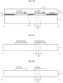
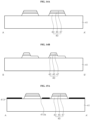
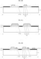
- FIGS. 4A , 4B, 5A, 5B , 6A, 6B, 7A , and 7B are schematic cross-sectional views illustrating a manufacturing process of the first floor
- FIGS. 8A, 8B , 9A, 9B 10A , 10B, 11A, 11B , 12A, 12B , 13A, and 13B are schematic cross-sectional views illustrating a manufacturing process of the second floor
- FIGS. 14A, 14B, 15A , 15B, 16A, 16B , 17A, and 17B are schematic cross-sectional views illustrating a manufacturing process of the third floor
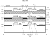
- 18A , 18B , 19A , and 19B are schematic cross-sectional views illustrating a process of manufacturing a pixel device by bonding the first through third floors.
- Each of the cross-sectional views corresponds to a view taken along line A-A' or B-B' in FIG. 3A , 3B , or 3C .
- LEDs 20 are formed on a substrate 21.
- the substrate 21 is a substrate on which a gallium nitride-based semiconductor layer can be grown, and may be, for example, a sapphire substrate.
- a first conductivity type semiconductor layer 23, an active layer 25, and a second conductivity type semiconductor layer 27 may be grown on the substrate 21 using, for example, metal organic chemical vapor deposition (MOCVD) technology or molecular beam epitaxy (MBE) technology.
- MOCVD metal organic chemical vapor deposition
- MBE molecular beam epitaxy
- the grown semiconductor layers may be patterned using photolithography and etching techniques.
- the second conductivity type semiconductor layer 27 and the active layer 25 may be partially removed such that a portion of the first conductivity type semiconductor layer 23 is exposed, and the LEDs 20 separated from one another may be formed through an isolation process. Although four LEDs 20 are shown in FIG. 3A , the inventive concepts are not limited thereto.
- FIG. 3A shows only one block for manufacturing the pixel device 100, and a plurality of blocks may be formed together on the substrate 21.
- a light blocking layer 213 may be formed on the substrate 21.
- the light blocking layer 213 surrounds the LEDs 20 and defines a window region 213a through which light is emitted.
- the window regions 213a formed by the light blocking layer 213 may be larger than or equal to bottom areas of the corresponding LEDs 20, respectively.
- an insulation layer 215 covering the LEDs 20 is formed.
- the insulation layer 215 may cover the light blocking layer 213.
- the insulation layer 215 may be patterned so as to expose the first conductivity type semiconductor layer 23.
- the insulation layer 215 may be patterned so as to expose the first conductivity type semiconductor layer 23 and to expose the second conductivity type semiconductor layer 27.
- first lower pads 217a1 and 217a2, first lower contacts 217c, and first lower connection lines 217b may be formed.
- the first lower contacts 217c may be electrically connected to the first conductivity type semiconductor layers 23 through the insulation layer 215.
- a planarization layer 221 covering the LEDs 20 is formed.
- the planarization layer 221 may cover the insulation layer 215, the first lower pads 217a1 and 217a2, the first lower contacts 217c, and the first lower connection lines 217b.
- the planarization layer 221 may be formed of a transparent insulating material such as polyimide or an epoxy molding compound.
- the planarization layer 221 covers a surface morphology formed by the LEDs 20 to provide a flat upper surface.
- first upper pads 291a1 and 291a2, first upper contacts 291c, and first upper connection lines 291b may be formed on the planarization layer 221.
- the second conductivity type semiconductor layer 27 may be partially exposed through the planarization layer 221 and the insulation layer 215, and the first upper contacts 291c may be electrically connected to the second conductivity type semiconductor layers 27 through the planarization layer 221 and the insulation layer 215.
- the first lower pads 271a1 and 271a2, the first lower contacts 271c, and the first lower connection lines 271c are formed under the planarization layer 221, but the inventive concepts are not limited thereto.
- the first lower pads 271a1 and 271a2, the first lower contacts 271c, and the first lower connection lines 271c may be formed on the planarization layer 221, and the first lower contacts 271c may be electrically connected to the first conductivity type semiconductor layer 23 through the planarization layer 221 and the insulation layer 215.
- additional pads may be formed on the planarization layer 221, and these pads may be electrically connected to the first lower pads 271a1 and 271a2 through connection vias passing through the planarization layer 221.
- LEDs 30 are formed on a substrate 31.
- the substrate 31 is a substrate on which a gallium nitride-based semiconductor layer can be grown, and may be, for example, a sapphire substrate.
- a first conductivity type semiconductor layer 33, an active layer 35, and a second conductivity type semiconductor layer 37 may be grown on a temporary substrate 31 using, for example, metal organic chemical vapor deposition (MOCVD) technology or molecular beam epitaxy (MBE) technology.
- MOCVD metal organic chemical vapor deposition
- MBE molecular beam epitaxy
- the grown semiconductor layers may be patterned using photolithography and etching techniques.
- the second conductivity type semiconductor layer 37 and the active layer 35 may be partially removed such that a portion of the first conductivity type semiconductor layer 33 is exposed, and the LEDs 30 separated from one another may be formed through an isolation process.
- the LEDs 30 may be formed in block units so as to correspond to the LEDs 20 formed on the first floor. Although four LEDs 30 are shown in FIG. 3B , the inventive concepts are not limited thereto.
- FIG. 3B shows only one block for manufacturing the pixel device 100, and a plurality of blocks may be formed together on the substrate 31.
- a light blocking layer 313 may be formed on the substrate 31.
- the light blocking layer 313 surrounds the LEDs 30 and defines a window region 313a through which light is emitted.
- the window regions 313a formed by the light blocking layer 313 may be larger than or equal to bottom areas of the corresponding LEDs 30, respectively.
- an insulation layer 315 covering the LEDs 30 is formed.
- the insulation layer 315 may cover the light blocking layer 313.
- the insulation layer 315 may be patterned so as to expose the first conductivity type semiconductor layer 33.
- the insulation layer 315 may be patterned so as to expose the first conductivity type semiconductor layer 33 and to expose the second conductivity type semiconductor layer 37.
- second lower pads 317a1 and 317a2, second lower contacts 317c, and second lower connection lines 317b may be formed.
- the second lower contacts 317c may be electrically connected to the first conductivity type semiconductor layers 33 through the insulation layer 315.
- a planarization layer 321 covering the LEDs 30 is formed.
- the planarization layer 321 may cover the insulation layer 315, the second lower pads 317a1 and 317a2, the second lower contacts 317c, and the first lower connection lines 317b.
- the planarization layer 321 may be formed of a transparent insulating material such as polyimide or an epoxy molding compound.
- the planarization layer 321 covers a surface morphology formed by the LEDs 30 to provide a flat upper surface.
- second upper pads 391a1 and 391a2, second upper contacts 391c, and second upper connection lines 391b may be formed on the planarization layer 321.
- the second conductivity type semiconductor layer 37 may be partially exposed through the planarization layer 321 and the insulation layer 315, and the second upper contacts 391c may be electrically connected to the second conductivity type semiconductor layers 37 through the planarization layer 321 and the insulation layer 315.
- the second lower pads 371a1 and 371a2, the second lower contacts 371c, and the second lower connection lines 371c are formed under the planarization layer 321, but the inventive concepts are not limited thereto.
- the second lower pads 371a1 and 371a2, the second lower contacts 371c, and the second lower connection lines 371c may be formed on the planarization layer 321, and the contacts 371c may be electrically connected to the first conductivity type semiconductor layer 33 through the planarization layer 321 and the insulation layer 315.
- additional pads may be formed on the planarization layer 321, and these pads may be electrically connected to the second lower pads 371a1 and 371a2 through connection vias passing through the planarization layer 321.
- a carrier substrate 331 may be attached to the planarization layer 321 using an adhesive tape 333.
- the carrier substrate 331 is not particularly limited, and may be, for example, a sapphire substrate.
- the adhesive tape 333 is for attaching the LEDs 30 to the carrier substrate 331, and any tape capable of reducing adhesion by heat or ultraviolet light may be used.
- the substrate 31 from the LEDs 30 may be removed.
- the substrate 31 may be removed using, for example, a laser lift off technique.
- LEDs 40 are formed on a substrate 41.
- the substrate 41 is a substrate on which a phosphorus nitride (GaP)-based semiconductor layer can be grown, and may be, for example, a GaAs substrate.
- a first conductivity type semiconductor layer 43, an active layer 45, and a second conductivity type semiconductor layer 47 may be grown on the substrate 41 using, for example, metal organic chemical vapor deposition (MOCVD) technology or molecular beam epitaxy (MBE) technology.
- MOCVD metal organic chemical vapor deposition
- MBE molecular beam epitaxy
- the grown semiconductor layers may be patterned using photolithography and etching techniques.
- the second conductivity type semiconductor layer 47 and the active layer 45 may be partially removed such that a portion of the first conductivity type semiconductor layer 43 is exposed, and the LEDs 40 separated from one another may be formed through an isolation process.
- the LEDs 40 may be formed in block units so as to correspond to the LEDs 20 formed on the first floor. Although four LEDs 40 are shown in FIG. 3C , the inventive concepts are not limited thereto.
- FIG. 3C shows only one block for manufacturing the pixel device 100, and a plurality of blocks may be formed together on the substrate 41.
- a light blocking layer 413 may be formed on the substrate 41.
- the light blocking layer 413 surrounds the LEDs 40 and defines a window region 413a through which light is emitted.
- the window regions 413a formed by the light blocking layer 413 may be larger than or equal to bottom areas of the corresponding LEDs 40, respectively.
- an insulation layer 415 covering the LEDs 40 is formed.
- the insulation layer 415 may cover the light blocking layer 413.
- the insulation layer 415 may be patterned so as to expose the first conductivity type semiconductor layer 43.
- the insulation layer 415 may be patterned so as to expose the first conductivity type semiconductor layer 43 and to expose the second conductivity type semiconductor layer 47.
- third lower pads 417a1 and 417a2, third lower contacts 417c, and third lower connection lines 417b may be formed.
- the third lower contacts 417c may be electrically connected to the first conductivity type semiconductor layers 43 through the insulation layer 415, respectively.
- a planarization layer 421 covering the LEDs 40 is formed.
- the planarization layer 421 may cover the insulation layer 415, the third lower pads 417a1 and 417a2, the third lower contacts 417c, and the first lower connection lines 417b.
- the planarization layer 421 may be formed of a transparent insulating material such as polyimide or an epoxy molding compound.
- the planarization layer 421 covers a surface morphology formed by the LEDs 40 to provide a flat upper surface.
- third upper pads 491a1 and 491a2, third upper contacts 491c, and third upper connection lines 491b may be formed on the planarization layer 421.
- the second conductivity type semiconductor layer 47 may be partially exposed through the planarization layer 421 and the insulation layer 415, and the third upper contacts 491c may be electrically connected to the second conductivity type semiconductor layers 47 through the planarization layer 421 and the insulation layer 415.
- the third lower pads 471a1 and 471a2, the third lower contacts 471c, and the third lower connection lines 471c are formed under the planarization layer 421, but the inventive concepts are not limited thereto.
- the third lower pads 471a1 and 471a2, the third lower contacts 471c, and the third lower connection lines 471c may be formed on the planarization layer 421, and the contacts 471c may be electrically connected to the first conductivity type semiconductor layer 43 through the planarization layer 421 and the insulation layer 415.
- additional pads may be formed on the planarization layer 421, and these pads may be electrically connected to the third lower pads 471a1 and 471a2 through connection vias passing through the planarization layer 421.
- the carrier substrate may be attached to the planarization layer 421 using the adhesive tape, and the substrate 41 may be removed using, for example, a wet etching technique.
- the second floor may be attached to the first floor using a lower adhesive layer 230
- the third floor may be attached to the second floor using an upper adhesive layer 340.
- the carrier substrate 331 and the adhesive tape 333 may be removed
- the carrier substrate and the adhesive tape may be removed. Accordingly, as shown in FIGS. 18A and 18B , a structure in which the first through third floors are stacked one above another is provided.
- an upper insulation layer 423 may be formed on the third floor.
- the upper insulation layer 423 may include an organic insulation layer or an inorganic insulation layer.
- the upper insulation layer 423, the planarization layers 221, 321, and 421, and the lower and upper adhesive layers 230 and 340 may be patterned to form via holes exposing the first through third lower pads 217a1, 271a2, 317a1, 317a2, 417a1, and 417a2 and the first through third upper pads 219a1, 219a2, 319a1, 319a2, 419a1, and 419a2.
- pixel device pads 50r1, 50r2, 50g1, 50g2, 50b1, 50b2, 50c1, and 50c2 and connection vias 50v may be formed on the upper insulation layer 423 so as to be electrically connected to the first through third lower pads 217a1, 271a2, 317a1, 317a2, 417a1, and 417a2 and the first through third upper pads 219a1, 219a2, 319a1, 319a2, 419a1, and 419a2.
- a plurality of blocks may be formed on the substrate 21, and these blocks may be singularized into individual blocks using a cutting technique. Accordingly, a plurality of individually separated pixel devices 100 is provided. The substrate 21 may be removed from the pixel devices 100.
- the LEDs 20, 30, or 40 are isolated from one another (isolation) on each independently manufactured floor, and the pads electrically connected to the LEDs 20, 30, and 40 are provided. Accordingly, after manufacturing each of the floors, it is possible to electrically and/or optically check whether or not the LEDs 20, 30, and 40 are defective before attaching the floors. Accordingly, since defective LEDs can be repaired in a state in which each of the floors is manufactured, a repair process may be easily performed, and thus, a process yield of the pixel device 100 may be improved.
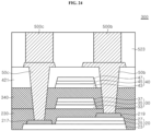
- FIG. 20 is a schematic cross-sectional view illustrating a pixel module 1000 including the pixel devices 100 according to an exemplary embodiment.
- the pixel devices 100 may be flip-bonded to a circuit board 1001 such that the pixel device pads 50r1, 50r2, 50g1, 50g2, 50b1, 50b2, 50c1, and 50c2 are electrically connected to the circuit board 1001.
- the pixel devices 100 are same as those described with reference to FIGS. 2A , 2B , and, a detailed description thereof is omitted to avoid redundancy.
- the pixel device pads may be bonded to pads 1003 on the circuit board 1001 through a bonding material 1005.
- a gap between the pads 1003 on the circuit board 1001 may be greater than a gap between the pixel device pads.
- the bonding materials 1005 may have a larger gap between lower surfaces than a gap between upper surfaces.
- a molding layer 1007 covering a plurality of pixel devices 100 may be formed over the pixel module 1000 in which the plurality of pixel devices 100 is arrayed.
- the molding layer 1007 is not particularly limited as long as it is a light-transmissive material.
- a thickness m1 of the pixel device 100 may be smaller than a distance m2 from an upper surface of the molding layer 1007 to an upper surface of the pixel device 100 in contact with the molding layer. Accordingly, the pixel module and the display apparatus can be made thinner, and thus, a distance between the user's eyes and the pixel device 100 may be reduced when viewed from the outside, thereby further improving visibility.
- FIG. 21 is a schematic diagram illustrating a pixel device according to an exemplary embodiment.
- FIG. 21 shows an example in which pixels are arranged in a 4 ⁇ 4 matrix.
- Each of pixels P includes vertically stacked LEDs 20, 30, and 40.
- the LEDs 20, 30, and 40 may be electrically connected to first through third lower connection lines 217b, 317b, and 417b and first through third upper connection lines 219b, 319b, and 419b such that the LEDs 20, 30, and 40 can be driven in a passive matrix manner.
- specific electrical connections of the LEDs 20, 30, and 40 are omitted.
- the first through third lower connection lines 217b, 317b, and 417b may be commonly electrically connected to cathodes of LEDs arranged in a same column. Since they are commonly electrically connected, the first through third lower connection lines 217b, 317b, and 417b are indicated by a same line in the drawing.
- the first through third lower connection lines 217b, 317b, and 417b disposed in the same column are electrically connected to a same pixel device pad 50c1, 50c2, 50c3, or 50c4. Accordingly, the pixel device pads 50c1, 50c2, 50c3, and 50c4 may be arranged in corresponding columns.
- the LEDs 20, 30, and 40 disposed in a same row are electrically connected to the first through third upper connection lines 219b, 319b, and 419b.
- the LEDs 20, 30, or 40 on a same floor are connected to a same upper connection line, but the LEDs disposed on different floors are connected to different upper connection lines.
- the LEDs 20 disposed on a first floor are connected to the first upper connection line 219b
- the LEDs 30 disposed on a second floor are connected to the second upper connection line 319b
- the LEDs 40 disposed on a third floor may be connected to the third upper connection line 419b.
- the pixel device pads 50c1, 50b1, 50g1, and 50r1 may be disposed in a first row in this order
- the pixel device pads 50b2, 50c2, 50g2, and 50r2 may be disposed in a second row in this order
- the pixel device pads 50b3, 50g3, 50c3, and 50r3 may be disposed in a third row
- the pixel device pads 50b4, 50g4, 50r4, and 50c4 may be disposed in a last row.
- an arrangement order of pixel device pads may be changed.
- the pixel device pads may be arranged in a same shape while maintaining a same distance from one another, but the inventive concepts are not limited thereto.
- FIG. 22A is a schematic plan view illustrating a pixel device 200 according to another exemplary embodiment of the present disclosure
- FIG. 22B is a schematic cross-sectional view taken along line C-C' of FIG. 22A
- FIG. 22C is a schematic cross-sectional view taken along line D-D' of FIG. 22A
- FIG. 22D is a schematic cross-sectional view taken along line E-E' of FIG. 22A
- FIGS. 23A through 23C show plan views of LEDs 20, 30, and 40 of first through third floors, respectively.
- the pixel device 200 may include a substrate 21, a planarization layer 421, lower and upper adhesive layers 230 and 340, the LEDs 20, 30, and 40, a first lower pad 217, a first upper pad 219, a second lower pad 317, a second upper pad 319, a third lower pad 417, a third upper pad 419, connection vias 50v, and pixel device pads 50r, 50g, 50b, and 50c.
- the pixel device 200 according to this embodiment is substantially similar to the pixel device 100 described with reference to FIGS. 2A through 2C , same or similar reference numerals are given to same components and detailed descriptions thereof are omitted to avoid redundancy.
- the pixel device 200 according to this embodiment as compared to the pixel device 100 described with reference to FIGS. 2A through 2C , has characteristics that first through third lower pads 217, 317, and 417 and first through third upper pads 219, 319, and 419 are disposed on respective corresponding LEDs 20, 30, and 40, and the LEDs 20, 30, and 40 partially overlap one another.
- the pixel device 200 may include the first through third floors disposed on the substrate 21, and these floors may be bonded through the adhesive layers 230 and 340, respectively.
- the first floor includes the LED 20, the first lower pad 217, and the first upper pad 219
- the second floor includes the LED 30, the second lower pad 317, and the second upper pad 319 as shown in FIG. 23B
- the third floor includes the LED 40, the third lower pad 417, and the third upper pad 419.
- the pixel device 200 is shown and described as having a single pixel, but may have a plurality of pixels. In this case, a plurality of LEDs is disposed on each of the floors, and the lower pads and the upper pads will be disposed on each of the LEDs.
- the substrate 21 is same as the substrate 21 described with reference to FIGS. 2A through 2C , a detailed description thereof is omitted to avoid redundancy.
- the substrate 21 may also be omitted.
- the pixel device 200 of this embodiment may also include at least one light blocking layer 213, 313, or 413 disposed around the LEDs 20, 30, and 40, as shown in FIGS. 2B and 2C , but they are omitted for convenience of description.
- the LED 20 may be patterned such that a portion of the first conductivity type semiconductor layer 23 is exposed through the second conductivity type semiconductor layer 27 and the active layer 25. As shown in FIG. 22B , a portion of an upper surface of the first conductivity type semiconductor layer 23 is exposed.
- the first conductivity type semiconductor layer 23 may be exposed in the peripheral region PA1.
- An upper surface of the substrate 21 may be exposed in regions other than the central region CA and the peripheral regions PA1 and PA2.
- the first lower pad 217 is disposed on the first conductivity type semiconductor layer 23 exposed in the peripheral region PA1, and the first upper pad 219 is disposed on the second conductivity type semiconductor layer in the peripheral region PA2.
- the first lower pad 217 and the first upper pad 219 may contact the first and second conductivity type semiconductor layers 23 and 27, respectively. Accordingly, in this embodiment, the lower connection lines are omitted. Furthermore, the first lower pad 217 and the first upper pad 219 may be formed directly on the LED 20, so that the insulation layer 215 and the planarization layer 221 described in the pixel device 100 may be omitted.
- the second floor may include the LED 30, the second lower pads 317, and the second upper pads 319.
- the second floor may be attached to the first floor by the lower adhesive layer 230.
- the lower adhesive layer 230 may cover the first lower pad 217, the LED 20, and the first upper pad 219. Further, the lower adhesive layer 230 may contact the substrate 21 exposed around the LED 20.
- the LED 30 may be patterned such that a portion of the first conductivity type semiconductor layer 33 is exposed through the second conductivity type semiconductor layer 37 and the active layer 35. As shown in FIG. 22C , a portion of an upper surface of the first conductivity type semiconductor layer 33 is exposed. The first conductivity type semiconductor layer 33 may be exposed in the peripheral region PA1 of the LED 30.
- the second lower pad 317 is disposed on the first conductivity type semiconductor layer 33 exposed in the peripheral region PA1, and the second upper pad 319 is disposed on the second conductivity type semiconductor layer 37 in the peripheral region PA2.
- the second lower pad 317 and the second upper pad 319 may contact the first and second conductivity type semiconductor layers 33 and 37, respectively. Accordingly, in this embodiment, the lower connection lines are omitted. Furthermore, the second lower pad 317 and the second upper pad 319 may be formed directly on the LED 30, so that the insulation layer 315 and the planarization layer 321 described in the pixel device 100 may be omitted.
- the third floor may include the LED 40, the third lower pad 417, and the third upper pad 419.
- the third floor may be attached to the second floor by the upper adhesive layer 340.
- the upper adhesive layer 340 may cover the LED 30, the second lower pad 317, and the second upper pad 319, and may also cover the lower adhesive layer 230.
- the LED 40 may be attached to the upper adhesive layer 340.
- the LED 40 is disposed so as to partially overlap the LED 30. Further, the LED 40 is disposed so as to partially overlap the LED 20.
- the LED 40 may include a central region CA and peripheral regions PA1 and PA2.
- the central region CA of the LED 40 may overlap the central regions CA of the LEDs 20 and 30, and the peripheral regions PA1 and PA2 of the LED 40 may be disposed on both sides of the central region CA so as not to overlap either the LED 20 or the LED, respectively.
- the peripheral regions PA1 and PA2 of the LED 40 may be disposed diagonally on left and right sides of the central region CA with respect to the central region CA.
- the peripheral region PA2 may extend rightward from one end of the central region CA, and the peripheral region PA1 may extend leftward from the other end of the central region CA. Since a material and a layer structure of the LED 40 are same as those described for the pixel device 100, detailed descriptions thereof are omitted.
- the LED 40 may be patterned such that a portion of the first conductivity type semiconductor layer 43 is exposed through the second conductivity type semiconductor layer 47 and the active layer 45. As shown in FIG. 22D , a portion of an upper surface of the first conductivity type semiconductor layer 43 is exposed. The first conductivity type semiconductor layer 43 may be exposed in the peripheral region PA1 of the LED 40.
- the third lower pad 417 is disposed on the first conductivity type semiconductor layer 43 exposed in the peripheral region PA1, and the third upper pad 419 is disposed on the second conductivity type semiconductor layer in the peripheral region PA2.
- the third lower pad 417 and the third upper pad 419 may contact the first and second conductivity type semiconductor layers 43 and 47, respectively. Accordingly, in this embodiment, the lower connection lines are omitted. Furthermore, the third lower pad 417 and the third upper pad 419 may be formed directly on the LED 40, so that the insulation layer 415 described in the pixel device 100 may be omitted.
- the planarization layer 421 covers the LED 40, the third lower pad 417, and the third upper pad 419.
- the planarization layer 421 may cover a surface morphology formed by the LEDs 40 to provide a flat upper surface.
- the planarization layer 421 may be formed of a light-transmitting insulating material such as polyimide (PI) or epoxy molding compound (EMC).
- the pixel device pads 50r, 50g, 50b, and 50c may be disposed on the third floor.
- the third upper pad 419 is disposed under the planarization layer 421, the upper insulation layer 423 of the pixel device 100 may be omitted.
- the pixel device pads 50r, 50g, 50b, and 50c may be disposed on the planarization layer 421.
- the pixel device pads 50r, 50g, 50b, and 50c may be electrically connected to the first through third lower pads 217, 317, and 417 and the first through third upper pads 219, 319, and 419 through the connection vias 50v.
- connection vias 50v are disposed on corresponding LEDs among the LEDs 20, 30, and 40, and may be laterally spaced apart from the other LEDs.
- the connection vias 50v do not pass through the LEDs 20, 30, and 40, and thus, there is no need to perform an etching process on the LEDs while the connection vias 50v are formed.
- the pixel device pad 50r may be electrically connected to the third upper pad 419 through the connection via 50v passing through the planarization layer 421.
- the pixel device pad 50g may be electrically connected to the second upper pads 319 through the connection via 50v passing through the planarization layer 421 and the upper adhesive layer 340.
- the pixel device pad 50b may be electrically connected to the first upper pad 219 through the connection via 50v passing through the planarization layer 421, the upper adhesive layer 340, and the lower adhesive layer 230.
- the pixel device pad 50c may be commonly electrically connected to the first through third lower pads 217, 317, and 417 through the connection via 50v.
- the pixel device pads 50c may be commonly electrically connected to the first lower pad 217, the second lower pad 317, and the third lower pad 417 through a plurality of connection vias 50v spaced apart from one another.
- the LED 20 may emit blue light
- the LED 30 may emit green light
- the LED 40 may emit red light
- the LED 20 may emit green light
- the LED 30 emit blue light
- the LED 40 emit red light.
- the pixel device 200 may be flip-bonded to a circuit board 1001 using the pixel device pads 50r, 50g, 50b, and 50c, and light generated from the LEDs 20, 30, and 40 may be emitted over the circuit board1001.
- the LEDs 20, 30, and 40 are partially vertically stacked one above another to constitute pixels.
- Each of the LEDs 20, 30, and 40 constitutes a sub-pixel.
- the LEDs 20, 30, and 40 are disposed on the first through third floors, respectively, and the lower pads 217, 317, and 417 and the upper pads 219, 318, and 419 connected to the LEDs 20, 30, and 40 are also disposed on corresponding floors.
- the pixel device 200 according to this embodiment may be manufactured in a substantially similar manner to that described in the manufacturing method of the pixel device 100, a detailed description thereof will be omitted to avoid redundancy.
- each of the floors is manufactured through different processes and then attached to one another using the lower and upper adhesive layers 230 and 340.
- electrical and/or optical characteristics of the LEDs 20, 30, or 40 in each of the floors may be evaluated to select defective LEDs, and repair may be performed for each of the floors.
- the defective LEDs may be easily repaired, and as a result, a process yield of the pixel device may be improved.
- the cathodes of the LEDs 20, 30, and 40 disposed on different floors are described as being commonly electrically connected to one another, and vice versa.
- a width of a region where the lower pads 217, 317, and 417 are disposed may be formed smaller than that of a light emitting region where the plurality of LEDs overlaps.
- at least one LED may have a groove such that the lower pads 217, 317, and 417 are disposed in a region protruding outward from the light emitting region.
- each of the lower pads 217, 317, and 417 may be disposed spaced apart so as not to overlap one another, and may be disposed in a groove region of an LED other than an LED electrically connected to other lower pad 217, 317, or 417.
- FIG. 24 is a schematic cross-sectional view illustrating a pixel device 300 according to another exemplary embodiment of the present disclosure.
- the pixel device 300 is substantially similar to the pixel device 200 described with reference to FIGS. 22A through 22D , except that it includes metal pads 500b and 500c and an upper insulating material layer 523.
- the upper insulating material layer 523 may be thicker than the planarization layer 421.
- the upper insulating material layer 523 may be formed of polyimide or an epoxy molding compound.
- the upper insulating material layer 523 may have openings exposing the pixel device pads 50r, 50g, 50g, and 50c, and the metal pads 500b and 500c may fill the openings in the upper insulating material layer 523.
- FIG. 24 shows two metal pads 500b and 500c formed on the pixel device pads 50b and 50c, the metal pads may also be disposed on the pixel device pads 50r and 50g.
- the metal pads may be electrically connected to corresponding pixel device pads 50r, 50g, 50b, and 50c.
- the metal pads 500b and 500c may function as final pixel device pads of the pixel device 300, and the pixel device pads 50r, 50g, 50g, and 50c may function as intermediate connection pads.
- the pixel device 300 may be mounted on the circuit board 1001 using the metal pads.
- the substrate 21 previously described may be omitted.
- the substrate 21 may be separated from the first floor using, for example, a laser lift-off technique or the like. Accordingly, the first floor may be exposed to the outside.
- FIG. 25 is a schematic cross-sectional view illustrating a pixel device 400 according to another exemplary embodiment of the present disclosure.
- the pixel device 400 according to this embodiment is substantially similar to the pixel device 100 described with reference to FIGS. 2A through 2C , same or similar reference numerals are given to same components and detailed descriptions thereof are omitted to avoid redundancy.
- the first through third lower contact layers 217c, 317c, and 417c are disposed on corresponding LEDs 20, 30, and 40, respectively, instead of the first through third lower contacts, the first through third lower connection lines, and the first through third lower pads of FIGS. 2A through 2C .
- the first through third lower contact layers 217c, 317c, and 417c are disposed on light exiting surfaces of corresponding LEDs 20, 30, and 40, respectively.
- the pixel device 400 may include first through third floors disposed on a substrate 401, and these floors may be bonded through the adhesive layers 230 and 340, respectively. As shown in FIG. 25 , the first lower contact layer 217c is disposed between the substrate 401 and the LEDs 20, the second lower contact layer 317c is disposed between the lower adhesive layer 230 and the LEDs 30, and the third lower contact layer 417c is disposed between the upper adhesive layer 340 and the LEDs 40.
- a plurality of LEDs may be disposed on each of the first through third floors, and the first through third lower contact layers 217c, 317c, and 417c may electrically connect adjacent LEDs. Furthermore, the first through third lower contact layers 217c, 317c, and 417c may extend to the outside of the LEDs 20, 30, and 40, respectively, and serve as pads to which the vias 50v are connected.
- the substrate 401 may be a substrate attached to the LED 20, unlike a growth substrate of the LED 20, and may be omitted.
- the LED 20 is disposed on the substrate 401. As described above, the LED 20 includes the first conductivity type semiconductor layer 23, the active layer 25, and the second conductivity type semiconductor layer 27.
- the first conductivity type semiconductor layer 23 of the LED 20 may include a first surface facing the active layer 25 and a second surface opposite the first surface, and a growth substrate is removed to expose the second surface of the first conductivity type semiconductor layer 23.
- the first lower contact layer 217c is disposed on the exposed second surface of the first conductivity type semiconductor layer 23, and the first upper contact layer 219c is disposed on the second conductivity type semiconductor layer.
- the first lower contact layer 217c may extend to the outside of the LED 20 and electrically connected to the pixel device pad 50c1 through the via 50v.
- the first lower contact layer 217c may electrically connect adjacent LEDs 20, and furthermore, a plurality of first lower contact layers 217c may be disposed.
- the first lower contact layers 217c may be electrically connected to different pixel device pads (e.g., 50c1 and 50c2 of FIG. 2A ).
- the first lower contact layer 217c includes a region overlapping the LED 20, and may additionally extend to the outside of the LED 20.
- the first lower contact layer 217c may be formed of a light-transmitting material such as a metallic material or a conductive oxide layer.
- the first lower contact layer 217c may be formed of a material that is transparent to light emitted from the LEDs 20, 30, and 40.
- the second floor may be attached to the first floor by the lower adhesive layer 230.
- the LEDs 30 may be arranged on the lower adhesive layer 230.
- the second lower contact layer 317c is disposed between the lower adhesive layer 230 and the LEDs 30.
- the LEDs 30 are disposed so as to at least partially overlap the LEDs 20, respectively.
- the first conductivity type semiconductor layer 33 of the LED 30 may include a first surface facing the active layer 35 and a second surface opposite to the first surface, and a growth substrate is removed to expose the first conductivity type semiconductor layer 33.
- the second lower contact layer 317c is disposed on the exposed second surface of the first conductivity type semiconductor layer 33, and the second upper contact layer 319c is disposed on the second conductivity type semiconductor layer.
- the second lower contact layer 317c and the second upper contact 319c may be electrically connected to the first and second conductivity type semiconductor layers 33 and 37, respectively.
- the second lower contact layer 317c may extend to the outside of the LED 30, and electrically connected to the pixel device pad 50c1 through the via 50v.
- the second lower contact layer 317c may electrically connect adjacent LEDs 30, and furthermore, a plurality of second lower contact layers 317c may be disposed.
- the second lower contact layers 317c may be electrically connected to different pixel device pads (e.g., 50c1 and 50c2 of FIG. 2A ).
- the second lower contact layer 317c includes a region overlapping the LED 30, and may additionally extend to the outside of the LED 30.
- the second lower contact layer 317c may be formed of a light-transmitting material such as a metallic material or a conductive oxide layer.
- the second lower contact layer 317c may be formed of a material that is transparent to light emitted from the LEDs 30 and 40.
- the third floor may be attached to the second floor by the upper adhesive layer 340.
- the LEDs 40 may be arranged on the upper adhesive layer 430.
- the third lower contact layer 417c is disposed between the upper adhesive layer 340 and the LEDs 40.
- the LEDs 40 are disposed so as to at least partially overlap the LEDs 30, respectively.
- the first conductivity type semiconductor layer 43 of the LED 40 may include a first surface facing the active layer 45 and a second surface opposite to the first surface, and a growth substrate is removed to expose the first conductivity type semiconductor layer 43.
- the third lower contact layer 417c is disposed on the exposed second surface of the first conductivity type semiconductor layer 43, and the third upper contact layer 419c is disposed on the second conductivity type semiconductor layer 47.
- the third lower contact layer 417c and the third upper contact 419c may be electrically connected to the first and second conductivity type semiconductor layers 43 and 47, respectively.
- the third lower contact layer 417c may extend to the outside of the LED 40, and electrically connected to the pixel device pad 50c1 through the via 50v.
- the third lower contact layer 417c may electrically connect adjacent LEDs 40, and furthermore, a plurality of third lower contact layers 417c may be disposed.
- the third lower contact layers 417c may be electrically connected to different pixel device pads (e.g., 50c1 and 50c2 of FIG. 2A ).
- the third lower contact layer 417c includes a region overlapping the LED 40, and may additionally extend to the outside of the LED 40.
- the third lower contact layer 417c may be formed of a light-transmitting material such as a metallic material or a conductive oxide layer.
- the third lower contact layer 417c may be formed of a material that is transparent to light emitted from the LEDs 40.
- the first through third lower contact layers 217c, 317c, and 417c may be directly connected to the via 50v, but the inventive concepts are not limited thereto.
- the first through third lower pads may be formed on the insulation layers 215, 315, and 415, respectively, may be electrically connected to the first through third lower contact layers 217c, 317c, and 417c, respectively, and the via 50v may be electrically connected through the first to third lower contact pads.
- the first through third lower pads may be formed of a material having a light transmittance different from those of the first through third lower contact layers 217c, 317c, and 417c.
Landscapes
- Led Device Packages (AREA)
Abstract
Description
- The present disclosure relates to a pixel device for an LED display that implements an image using a light emitting diode and a display apparatus having the same.
- Light emitting diodes are inorganic light sources, which are used in various fields such as display apparatuses, automobile lamps, general lighting, and the like. The light emitting diodes have advantages such as longer lifespan, lower power consumption, and quicker response, than conventional light sources, and thus, they have been replacing the conventional light sources.
- The conventional light emitting diodes have been generally used as backlight light sources in display apparatuses. However, LED displays that directly realize images using the light emitting diodes have been recently developed.
- In general, the display apparatus displays various colors through mixture of blue, green, and red light. In order to realize various images, the display apparatus includes a plurality of pixels, each of the pixels includes sub-pixels of blue, green, and red light, a color of a certain pixel is determined based on colors of the sub-pixels, and images can be realized through a combination of such pixels.
- An LED display apparatus implements an image by using a very small LED in a micro unit. To manufacture the LED display apparatus, numerous pixel devices are manufactured, and the pixel devices are mounted on a circuit board using pads formed on the pixel devices. Each of the pixel devices includes one or more pixels. The pixel device may include a pixel in which LEDs are laterally arranged or a pixel in which LEDs are vertically stacked.
- The pixel of a vertically stacked structure is generally manufactured by bonding semiconductor layers grown on different growth substrates using a wafer-wafer bonding technique. The pixel device is manufactured by patterning semiconductor layers bonded to one another at a wafer level, forming an electrode structure for electrical connection, and thereafter, dividing the pixel device into individual pixel device units.
- According to a prior art, since the electrode structure is formed after bonding the semiconductor layers, etching for different materials such as semiconductor layers and insulation layers is required, and since etching is required through several layers, it is difficult to generate a hole having a relatively large aspect ratio. Accordingly, it is difficult to form the electrode structure, and a pixel manufacturing process is complicated.
- Furthermore, since electrical characteristics or optical characteristics can be measured after the pixel device is completed, whether or not the pixel device is defective can be checked only after the pixel device is completed. When a defective pixel device is identified, the defective pixel device is discarded or repaired. Since blue, green, and red LEDs have a stacked structure, even when a defect occurs in any one of the LEDs, it leads to a defect in the pixel device, resulting in a very low yield of the pixel devices. In addition, even when the defective pixel device is repaired, since a repair process has to be performed after a final pixel device is completed, it is relatively difficult to repair the pixel device. Accordingly, even when repair is possible, the defective pixel device is often discarded instead of repairing it due to drawbacks such as process complexity and cost, and thus, it is difficult to increase a process yield of pixel devices through repair.
- Exemplary embodiments of the present disclosure provide a pixel device having a structure in which LEDs are vertically stacked and having a novel structure that is configured to increase a process yield, and a display apparatus having the same.
- Exemplary embodiments of the present disclosure provide a pixel device that is configured to easily repair defective LEDs during a manufacturing process and a display apparatus having the same.
- Exemplary embodiments of the present disclosure may simplify a manufacturing process and provide a pixel device in which an electrode structure is easily formed and a display apparatus having the same.
- A pixel device according to an exemplary embodiment includes a first floor including a first LED, and a first lower pad and a first upper pad electrically connected to the first LED; a second floor disposed over the first floor, and including a second LED, and a second lower pad and a second upper pad electrically connected to the second LED; and a third floor disposed over the second floor, and including a third LED, and a third lower pad and a third upper pad electrically connected to the third LED.
- As used herein, a term "pixel device" refers to a unit device configured to be mounted on a circuit board. The pixel device may include one or more pixels. Meanwhile, the pixel is generally a basic unit constituting an image in a display. To implement a color image, one pixel may include at least three sub-pixels each emitting a single color. Structurally, a term "pixel" refers to a combination of the sub-pixels, and the sub-pixels are stacked one above another.
- The first LED, the second LED, and the third LED may emit visible light of different colors from one another. For example, the first LED may emit blue light, the second LED may emit green light, and the third LED may emit red light. In another embodiment, the first LED may emit green light, the second LED may emit blue light, and the third LED may emit red light.
- The first through third lower pads may be electrically connected to one another, and the first through third upper pads may be electrically spaced apart from one another.
- The pixel device may include a lower adhesive layer bonding the first floor and the second floor; and an upper adhesive layer bonding the second floor and the third floor.
- The first through third LEDs may be disposed so as to overlap one another in a vertical direction. A pixel is provided by the first through third LEDs overlapping in the vertical direction.
- The first through third LEDs may partially overlap one another.
- The pixel device may further include a light blocking layer surrounding the first LED, the second LED, or the third LED.
- The first floor may further include a first insulation layer covering the first LEDs and a first planarization layer covering the insulation layer, and the first upper pad may be disposed on the first planarization layer. Furthermore, the first lower pad may be disposed between the first insulation layer and the first planarization layer or on the first planarization layer.
- The second floor may further include a second insulation layer covering the second LEDs and a second planarization layer covering the second insulation layer, and the second upper pad may be disposed on the second planarization layer. Furthermore, the second lower pad may be disposed between the second insulation layer and the second planarization layer or on the second planarization layer.
- The third floor may further include a third insulation layer covering the third LEDs and a third planarization layer covering the third insulation layer, and the third upper pad may be disposed on the third planarization layer. Furthermore, the third lower pad may be disposed between the third insulation layer and the third planarization layer or on the third planarization layer.
- The pixel device may further include an upper insulation layer covering the third floor and pixel device pads disposed on the upper insulation layer. Each of the pixel device pads may be electrically connected to at least one of the first through third lower pads and the first through third upper pads.
- A plurality of first LEDs, a plurality of second LEDs, and a plurality of third LEDs may be arranged in a matrix of n×m (n, m is a positive integer) on the first through third floors, respectively, and the number of pixel pad electrodes may be (3n+m).
- The pixel device pads may be electrically connected to at least one of the first through third lower pads and the first through third upper pads through connection vias. The connection vias may be spaced apart from the first through third LEDs in a lateral direction.
- The first through third lower pads may be electrically connected to cathodes of the first through third LEDs, respectively, and the first through third upper pads may be electrically connected to anodes of the first through third LEDs, respectively.
- A display apparatus according to an embodiment of the present disclosure includes a circuit board and a pixel device disposed on the circuit board, in which the pixel device includes a first floor including a first LED, and a first lower pad and a first upper pad electrically connected to the first LED; a second floor disposed over the first floor, and including a second LED, and a second lower pad and a second upper pad electrically connected to the second LED; and a third floor disposed over the second floor, and including a third LED, and a third lower pad and a third upper pad electrically connected to the third LED.
- The pixel device may further include an upper insulation layer disposed on the third floor and pixel device pads disposed on the upper insulation layer, and the pixel device pads may be bonded to the circuit board.
- The pixel device pads may be electrically connected to at least one of the first through third lower pads and the first through third upper pads through connection vias, and the connection vias may be spaced apart from the first through third LEDs in a lateral direction.
-
-
FIG. 1A is a schematic plan view illustrating a display apparatus according to an exemplary embodiment. -
FIG. 1B are schematic perspective views illustrating various display apparatuses according to an exemplary embodiment. -
FIG. 1C is a schematic perspective view illustrating another display apparatus according to an exemplary embodiment. -
FIG. 1D is a schematic perspective view illustrating another display apparatus according to an exemplary embodiment. -
FIG. 2A is a schematic plan view illustrating a pixel device according to an exemplary embodiment. -
FIG. 2B is a schematic cross-sectional view taken along line A-A' ofFIG. 2A . -
FIG. 2C is a schematic cross-sectional view taken along line B-B' ofFIG. 2A . -
FIG. 3A is a schematic plan view illustrating a first floor ofFIG. 2A . -
FIG. 3B is a schematic plan view illustrating a second floor ofFIG. 2A . -
FIG. 3C is a schematic plan view illustrating a third floor ofFIG. 2A . -
FIGS. 4A ,4B, 5A, 5B ,6A, 6B, 7A , and7B are schematic cross-sectional views illustrating a manufacturing process of the first floor. -
FIGS. 8A, 8B ,9A, 9B ,10A ,10B, 11A, 11B ,12A, 12B ,13A, and 13B are schematic cross-sectional views illustrating a manufacturing process of the second floor. -
FIGS. 14A, 14B, 15A ,15B, 16A, 16B ,17A, and 17B are schematic cross-sectional views illustrating a manufacturing process of the third floor. -
FIGS. 18A ,18B ,19A , and19B are schematic cross-sectional views illustrating a process of manufacturing a pixel device by bonding the first through third floors. -
FIG. 20 is a schematic cross-sectional view illustrating a pixel module including pixel devices according to an exemplary embodiment. -
FIG. 21 is a schematic diagram illustrating a pixel device according to an exemplary embodiment. -
FIG. 22A is a schematic plan view illustrating a pixel device according to another exemplary embodiment of the present disclosure. -
FIG. 22B is a schematic cross-sectional view taken along line C-C' ofFIG. 22A . -
FIG. 22C is a schematic cross-sectional view taken along line D-D' ofFIG. 22A . -
FIG. 22D is a schematic cross-sectional view taken along line E-E' ofFIG. 22A . -
FIG. 23A is a schematic plan view illustrating a first floor ofFIG. 22A . -
FIG. 23B is a schematic plan view illustrating a second floor ofFIG. 22A . -
FIG. 23C is a schematic plan view illustrating a third floor ofFIG. 22A . -
FIG. 24 is a schematic cross-sectional view illustrating a pixel device according to another exemplary embodiment. -
FIG. 25 is a schematic cross-sectional view illustrating a pixel device according to another exemplary embodiment. - Hereinafter, exemplary embodiments of the present disclosure will be described in detail with reference to the accompanying drawings. The following exemplary embodiments are provided by way of example so as to fully convey the spirit of the present disclosure to those skilled in the art to which the present disclosure pertains. Accordingly, the present disclosure is not limited to the embodiments disclosed herein and can also be implemented in different forms. In the drawings, widths, lengths, thicknesses, and the like of elements can be exaggerated for clarity and descriptive purposes. When an element or layer is referred to as being "disposed above" or "disposed on" another element or layer, it can be directly "disposed above" or "disposed on" the other element or layer or intervening elements or layers can be present. Throughout the specification, like reference numerals denote like elements having the same or similar functions.
-
FIG. 1A is a schematic plan view illustrating a display apparatus according to an exemplary embodiment, andFIGS. 1B ,1C , and1D are schematic perspective views illustratingvarious display apparatuses - Referring to
FIG. 1A , adisplay apparatus 10000 may include apanel substrate 2100 and a plurality ofpixel modules 1000. - The
display apparatus 10000 is not particularly limited, but may include asmart watch 1000a, awearable display apparatus 1000b such as a VR headset or glasses, anAR display apparatus 1000c such as augmented reality glasses, or an indoor oroutdoor display apparatus panel substrate 2100 and the plurality ofpixel modules 1000 may be disposed in the display apparatus. A gap between pixels in the display apparatus may be very narrow, for example, the gap between pixels may be 0.01 mm or less. The display apparatus may implement an image through pixels mounted on a circuit board or a transparent substrate. In some display apparatuses, a distance between the display apparatus and an external receiver (e.g., a user's eyes) that recognizes the display may be 200 mm or less. The gap between pixels may be 0.005% to 0.1% of the distance between the external receiver and the display apparatus. The display apparatus may transmit an optical signal from a substrate including a curved surface to the external receiver. The display apparatus may also be a transparent display apparatus using a transparent substrate. - The
panel substrate 2100 may include a circuit for a passive matrix driving or active matrix driving manner. In an exemplary embodiment, thepanel substrate 2100 may include wirings and resistors therein, and, in another exemplary embodiment, thepanel substrate 2100 may include wirings, transistors, and capacitors. Thepanel substrate 2100 may also have pads that are capable of being electrically connected to the disposed circuit on an upper surface thereof. - In an exemplary embodiment, the plurality of
pixel modules 1000 is arranged on thepanel substrate 2100. Each of thepixel modules 1000 may include acircuit board 1001, and a plurality ofpixel devices 100 disposed on thecircuit board 1001, and may include a molding member covering thepixel devices 100. In another exemplary embodiment, the plurality ofpixel devices 100 may be directly arranged on thepanel substrate 2100, and the molding member may cover thepixel devices 100. - The
smart watch 1000a may be 500 to 1500cd/m2 (or nits) or more, and a brightness thereof may be adjusted according to an external illumination. Thewearable display apparatus 1000b such as a VR headset or glasses may be 150 to 200 cd/m2 (or nits), or a viewing angle thereof may be 50 degrees or more. The indoor oroutdoor display apparatus display apparatus - Hereinafter, a
pixel device 100 according to an exemplary embodiment will be described in detail with reference toFIGS. 2A ,2B ,2C ,3A ,3B , and3C . -
FIG. 2A is a schematic plan view illustrating thepixel device 100 according to an exemplary embodiment, andFIGS. 2B and2C are schematic cross-sectional views taken along lines A-A' and BB' ofFIG. 2A , respectively. The pixel device includes a plurality of floors, and each of the floors is shown inFIGS 3A ,3B and3C . Herein, a pixel device including pixels arranged in a 2×2 matrix will be described as an example. - Referring to
FIGS. 2A ,2B , and2C , thepixel device 100 may include asubstrate 21, light blocking layers 213, 313, and 413, insulation layers 215, 315, and 415, planarization layers 221, 321 and 421, lower and upperadhesive layers LEDs lower connection lines 217b, and firstlower contacts 217c, first upper pads 219a1 and 219a2, firstupper connection lines 219b, firstupper contacts 219c, second lower pads 317a1 and 317a2, secondlower connection lines 317b, secondlower contacts 317c, second upper pads 319a1 and 319a2, secondupper connection lines 319b, secondupper contacts 319c, third lower pads 417a1 and 417a2, thirdlower connection lines 417b, thirdlower contacts 417c, third upper pads 419a1 and 419a2, thirdupper connection lines 419b, thirdupper contacts 419c, anupper insulation layer 423,connection vias 50v, and pixel device pads 50r1, 50r2, 50g1, 50g2, 50b1, 50b2, 50c1, and 50c2. - In particular, the
pixel device 100 may include first through third floors disposed on thesubstrate 21, and these floors may be bonded through theadhesive layers LEDs 20, the first lower pads 217a1 and 217a2, the firstlower connection lines 217b, the firstlower contacts 217c, the first upper pads 219a1 and 219a2, the firstupper connection lines 219b, and the firstupper contacts 219c, and the second floor includes theLEDs 30, the second lower pads 317a1 and 317a2, the secondlower connection lines 317b, the secondlower contacts 317c, the second upper pads 319a1 and 319a2, the secondupper connection lines 319b, and the secondupper contacts 319c, and the third floor includes theLEDs 40, the third lower pads 417a1 and 417a2, the thirdlower connection lines 417b, the thirdlower contacts 417c, the third upper pads 419a1 and 419a2, the thirdupper connection lines 419b, and the thirdupper contacts 419c. - The
substrate 21 is a transparent substrate that transmits light generated in thepixels substrate 21 may be translucent or partially transparent so as to transmit only light of a specific wavelength or only a portion of light of a specific wavelength. Thesubstrate 21 may include glass, quartz, silicon, an organic polymer, or an organic-inorganic composite material, for example, silicon carbide (SiC), gallium nitride (GaN), indium gallium nitride (InGaN), aluminum gallium nitride (AlGaN), aluminum nitride (AlN), gallium oxide (Ga2O3) substrate, and the like. Thesubstrate 21 may be omitted. - Referring to
FIGS. 2A ,2B ,2C , and3A , theLEDs 20 are arranged on thesubstrate 21. In this embodiment, it is described that fourLEDs 20 are arranged, but the inventive concepts are not limited thereto. For example, oneLED 20 may be disposed on thesubstrate 21, or two ormore LEDs 20 may be disposed. - Each of the
LEDs 20 includes a first conductivitytype semiconductor layer 23, anactive layer 25, and a second conductivitytype semiconductor layer 27. Theactive layer 25 may be disposed between the first conductivitytype semiconductor layer 23 and the second conductivitytype semiconductor layer 27. The first conductivitytype semiconductor layer 23 may be, for example, an n-type conductivity type semiconductor layer, and the second conductivitytype semiconductor layer 27 may be a p-type conductivity type semiconductor layer, and vice versa. In an embodiment, theLED 20 may include a semiconductor material that emits blue light, such as GaN, InGaN, ZnSe, or the like, without being limited thereto, and may emit red or green light. - The
LED 20 may be patterned such that a portion of the first conductivitytype semiconductor layer 23 is exposed through the second conductivitytype semiconductor layer 27 and theactive layer 25. As shown inFIG. 2C , a portion of an upper surface of the first conductivitytype semiconductor layer 23 is exposed. In this embodiment, it is shown that the second conductivitytype semiconductor layer 27 and theactive layer 25 are partially removed near an edge of the first conductivitytype semiconductor layer 23, but the inventive concepts are not limited thereto, and a through hole passing through the second conductivitytype semiconductor layer 27 and theactive layer 25 may be formed to expose the first conductivitytype semiconductor layer 23. - A
light blocking layer 213 is disposed on thesubstrate 21. Thelight blocking layer 213 surrounds theLEDs 20 and defines awindow region 213a through which light is emitted. Thelight blocking layer 20 may be formed of, for example, a black matrix, and may improve a contrast ratio by preventing cross-talk between theLEDs display apparatus 10000. Thelight blocking layer 213 may be omitted. - The
window region 213a through which light is emitted to the outside may be larger than or equal to a lower surface area of theLED 20. In an embodiment, theLED 20 may be in contact with thelight blocking layer 213. - The
insulation layer 215 covers theLEDs 20. Additionally, theinsulation layer 215 may cover thelight blocking layer 213. Theinsulation layer 215 may be formed of a light-transmitting material. For example, theinsulation layer 215 may include silicon oxide such as SiO2, silicon nitride such as Si3N4, or silicon oxynitride. - The
insulation layer 215 may be patterned so as to allow electrical connection to the first conductivitytype semiconductor layer 23 and the second conductivitytype semiconductor layer 27. For example, theinsulation layer 215 may have openings exposing the first conductivitytype semiconductor layer 23 and the second conductivitytype semiconductor layer 27. A transparent electrode may be formed on the second conductivitytype semiconductor layer 27, and in this case, the opening of theinsulation layer 215 may expose the transparent electrode. - The first lower pads 217a1 and 217a2, the first
lower connection lines 217b, and the firstlower contacts 217c are formed on theinsulation layer 215. The firstlower contacts 217c are electrically connected to the first conductivitytype semiconductor layer 23 of theLEDs 20. The firstlower contact 217c may be connected to the first conductivitytype semiconductor layer 23 through the opening of theinsulation layer 215. Since the firstlower contacts 217c are disposed on theLEDs 20, respectively, the number of firstlower contacts 217c is at least equal to the number of theLEDs 20. - The first lower pads 217a1 and 217a2 may be spaced apart from the
LEDs 20 in a lateral direction and disposed on theinsulation layer 215. In an embodiment, both of the first lower pads 217a1 and 217a2 are spaced apart from theLEDs 20 and disposed near one side (lower side) of thesubstrate 21, as shown inFIG. 3A . However, the inventive concepts are not limited thereto, and at least one of the first lower pads 217a1 and 217a2 may be disposed in a region between theLEDs 20. In an embodiment, the first lower pads 217a1 and 217a2 may be disposed at least as many as the number of columns of theLEDs 20. In this embodiment, since theLEDs 20 are disposed in two rows, two first lower pads 217a1 and 217a2 are disposed. - The first
lower connection lines 217b connect the firstlower contacts 217c to the first lower pads 217a1 and 217a2. As shown inFIG. 3A , the firstlower connection lines 217b may electrically connect the firstlower contacts 217c on theLEDs 20 disposed in a same column to a same first lower pad 217a1 or 217a2. That is, one firstlower connection line 217b connects the firstlower contacts 217c disposed in a first column to the first lower pad 217a1, and another firstlower connection line 217b connects the firstlower contacts 217c disposed in a second column to the first lower pad 217a2. The firstlower connection lines 217b may be provided in a same number as those of the first lower pads 217a1 and 217a2. - The
planarization layer 221 covers theLEDs 20, theinsulation layer 215, the first lower pads 217a1 and 217a2, the firstlower contacts 217c, and the firstlower connection lines 217b. Theplanarization layer 221 may cover a surface morphology formed by theLEDs 20 to provide a flat upper surface. Theplanarization layer 221 may be formed of a light-transmitting insulating material such as polyimide (PI) or epoxy molding compound (EMC). - The first upper pads 219a1 and 219a2, the first
upper connection lines 219b, and the firstupper contacts 219c are formed on theplanarization layer 221. The firstupper contacts 219c are electrically connected to the second conductivity type semiconductor layers 27 of theLEDs 20. The firstupper contact 219c may be electrically connected to the second conductivity type semiconductor layers 27 through theplanarization layer 221 and theinsulation layer 215. Since the firstupper contacts 219c are disposed on theLEDs 20, respectively, the number of firstupper contacts 219c is at least equal to the number of theLEDs 20. - The first upper pads 219a1 and 219a2 may be spaced apart from the
LEDs 20 in the lateral direction and disposed on theplanarization layer 221. Also, the first upper pads 219a1 and 219a2 are spaced apart from the first lower pads 217a1 and 217a2 in the lateral direction. That is, the first upper pads 219a1 and 219a2 are disposed on theplanarization layer 221 so as not to overlap the first lower pads 217a1 and 217a2. In an embodiment, both of the first upper pads 219a1 and 219a2 may be spaced apart from theLEDs 20 and disposed near one side (right side) of thesubstrate 21, as shown inFIG. 3A . However, the inventive concepts are not limited thereto, and at least one of the first upper pads 219a1 and 219a2 may be disposed in the region between theLEDs 20. In an embodiment, the first upper pads 217a1 and 217a2 may be disposed at least as many as the number of rows of theLEDs 20. In this embodiment, since theLEDs 20 are disposed in two rows, two first upper pads 219a1 and 219a2 are disposed. - The first
upper connection lines 219b connect the firstupper contacts 219c to the first upper pads 219a1 and 219a2. As shown inFIG. 3A , the firstupper connection lines 219b may connect the firstupper contacts 219c on theLEDs 20 arranged in a same row to a same first upper pad 219a1 or 219a2. That is, one firstupper connection line 219b connects the firstupper contacts 219c disposed in a first row to the first upper pad 219a1, and another firstupper connection line 219b connects the firstupper contacts 219c disposed in a second row to the first upper pad 219a2. The firstupper connection lines 219b may be provided in a same number as those of the first upper pads 219a1 and 219a2. - In this embodiment, the first lower pads 217a1 and 217a2 are illustrated and described as being disposed between the
insulation layer 215 and theplanarization layer 221, but the inventive concepts are not limited thereto. For example, the first lower pads 217a1 and 217a2, the firstlower contacts 217c, and the firstlower connection lines 217b may be disposed on theplanarization layer 221, and the firstlower contacts 217c may be electrically connected to the first conductivitytype semiconductor layer 23 through theplanarization layer 221 and theinsulation layer 215. In another embodiment, in addition to the first lower pads 217a1 and 217a2 disposed on theinsulation layer 215, additional pads electrically connected to the first lower pads 217a1 and 217a2 may be provided on theplanarization layer 221. - The second floor may include the
LEDs 30, thelight blocking layer 313, theinsulation layer 315, the secondlower contacts 317c, the second lower pads 317a1 and 317a2, the secondlower connection lines 317b, theplanarization layer 321, the secondupper contacts 319c, the second upper pads 319a1 and 319a2, and the secondupper connection lines 319b. The second floor may be attached to the first floor by the loweradhesive layer 230. - The lower
adhesive layer 230 covers the firstupper contacts 219c, the first upper pads 219a1 and 219a2, the firstupper connection lines 219b, and theplanarization layer 221. The loweradhesive layer 230 may include an optically clear adhesive (OCA), which, for example, may include epoxy, polyimide, SU8, spin-on-glass (SOG), benzocyclobutene (BCB), without being limited thereto. - The
LEDs 30 may be attached to the loweradhesive layer 230. In this embodiment, it is described that fourLEDs 30 are arranged, but the inventive concepts are not limited thereto. TheLEDs 30 may be arranged in a same number as that of theLEDs 20, and may be arranged such that at least a portion of a light emitting region overlaps theLEDs 20. - Each of the
LEDs 30 includes a first conductivitytype semiconductor layer 33, anactive layer 35, and a second conductivitytype semiconductor layer 37. Theactive layer 35 may be disposed between the first conductivitytype semiconductor layer 33 and the second conductivitytype semiconductor layer 37. The first conductivitytype semiconductor layer 33 may be, for example, an n-type conductivity type semiconductor layer, and the second conductivitytype semiconductor layer 37 may be a p-type conductivity type semiconductor layer, and vice versa. In an embodiment, theLED 30 may include a semiconductor material that emits green light, such as GaN, InGaN, GaP, AlGaInP, AlGaP, or the like, without being limited thereto, and may emit red or blue light. - The
LED 30 may be patterned such that a portion of the first conductivitytype semiconductor layer 33 is exposed through the second conductivitytype semiconductor layer 37 and theactive layer 35. As shown inFIG. 2C , a portion of an upper surface of the first conductivitytype semiconductor layer 33 is exposed. In this embodiment, it is shown that the second conductivitytype semiconductor layer 37 and theactive layer 35 are partially removed near an edge of the first conductivitytype semiconductor layer 33, but the inventive concepts are not limited thereto, and a through hole passing through the second conductivitytype semiconductor layer 37 and theactive layer 35 may be formed to expose the first conductivitytype semiconductor layer 33. - The
light blocking layer 313 is disposed on the loweradhesive layer 230. Thelight blocking layer 313 surrounds theLEDs 30 and defines awindow region 313a through which light is emitted. Thelight blocking layer 313 may be formed of, for example, a black matrix, and may improve a contrast ratio by preventing cross-talk between theLEDs display apparatus 10000. Thelight blocking layer 313 may be omitted. - The
window region 313a formed by thelight blocking layer 313 may be larger than or equal to a lower surface area of theLED 30. In an embodiment, theLED 30 may be in contact with thelight blocking layer 313. - The
insulation layer 315 covers theLEDs 30. Theinsulation layer 315 may also cover thelight blocking layer 313. Theinsulation layer 315 may be formed of a light-transmitting material. For example, theinsulation layer 315 may include silicon oxide such as SiO2, silicon nitride such as Si3N4, or silicon oxynitride. - The
insulation layer 315 may be patterned so as to allow electrical connection to the first conductivitytype semiconductor layer 33 and the second conductivitytype semiconductor layer 37. For example, theinsulation layer 315 may have openings exposing the first conductivitytype semiconductor layer 33 and the second conductivitytype semiconductor layer 37. A transparent electrode may be formed on the second conductivitytype semiconductor layer 37, and in this case, the opening of theinsulation layer 315 may expose the transparent electrode. - The second lower pads 317a1 and 317a2, the second
lower connection lines 317b, and the secondlower contacts 317c are formed on theinsulation layer 315. The secondlower contacts 317c are electrically connected to the first conductivitytype semiconductor layer 33 of theLEDs 30. The secondlower contact 317c may be connected to the first conductivitytype semiconductor layer 33 through the opening of theinsulation layer 315. Since the secondlower contacts 317c are disposed on theLEDs 30, respectively, the number of secondlower contacts 317c is at least equal to the number of theLEDs 30. - The second lower pads 317a1 and 317a2 may be spaced apart from the
LEDs 30 in the lateral direction and disposed on theinsulation layer 315. In an embodiment, the second lower pads 317a1 and 317a2 may be disposed so as to overlap the first lower pads 217a1 and 217a2, respectively. For example, both of the second lower pads 317a1 and 317a2 may be spaced apart from theLEDs 30 and disposed near one side (lower side) of thesubstrate 21, as shown inFIG. 3B . However, the inventive concepts are not limited thereto, and at least one of the second lower pads 317a1 and 317a2 may be disposed in a region between theLEDs 30. Also, the second lower pads 317a1 and 317a2 may be laterally spaced apart from the first lower pads 217a1 and 217a2 so as to partially overlap or so as not to overlap the first lower pads 217a1 and 217a2. In an embodiment, the second lower pads 317a1 and 317a2 may be disposed at least as many as the number of columns of theLEDs 30. In this embodiment, since theLEDs 30 are disposed in two rows, two second lower pads 317a1 and 317a2 are disposed. - The second
lower connection lines 317b electrically connect the secondlower contacts 317c to the second lower pads 317a1 and 317a2. As shown inFIG. 3A , the secondlower connection lines 317b may connect the secondlower contacts 317c on theLEDs 30 disposed in a same column to a same second lower pad 317a1 or 317a2. That is, one secondlower connection line 317b connects the secondlower contacts 317c disposed in a first column to the second lower pad 317a1, and another secondlower connection line 317b connects the secondlower contacts 317c disposed in a second column to the second lower pad 317a2. The secondlower connection lines 317b may be provided in a same number as those of the second lower pads 317a1 and 317a2. - The
planarization layer 321 covers theLEDs 30, theinsulation layer 315, the second lower pads 317a1 and 317a2, the secondlower contacts 317c, and the secondlower connection lines 317b. Theplanarization layer 321 may cover a surface morphology formed by theLEDs 30 to provide a flat upper surface. Theplanarization layer 321 may be formed of a light-transmitting insulating material such as polyimide (PI) or epoxy molding compound (EMC). - The second upper pads 319a1 and 319a2, the second
upper connection lines 319b, and the secondupper contacts 319c are formed on theplanarization layer 321. The secondupper contacts 319c are electrically connected to the second conductivity type semiconductor layers 37 of theLEDs 30. The secondupper contact 319c may be electrically connected to the second conductivity type semiconductor layers 37 through theplanarization layer 321 and theinsulation layer 315. Since the secondupper contacts 319c are disposed on theLEDs 30, respectively, the number of secondupper contacts 319c is at least equal to the number of theLEDs 30. - The second upper pads 319a1 and 319a2 may be spaced apart from the
LEDs 30 in the lateral direction and disposed on theplanarization layer 321. Also, the second upper pads 319a1 and 319a2 are spaced apart from the second lower pads 317a1 and 317a2 in the lateral direction. Furthermore, the second upper pads 319a1 and 319a2 may be spaced apart from the first upper pads 219a1 and 219a2 in the lateral direction. That is, the second upper pads 319a1 and 319a2 may be disposed on theplanarization layer 321 so as not to overlap the first lower pads 217a1 and 217a2, the first upper pads 219a1 and 219a2, and the second lower pads 317a1 and 317a2. In an embodiment, both of the second upper pads 319a1 and 319a2 may be spaced apart from theLEDs 30 and disposed near one side (left side) of thesubstrate 21, as shown inFIG. 3B . However, the inventive concepts are not limited thereto, and at least one of the second upper pads 319a1 and 319a2 may be disposed in the region between theLEDs 30. In an embodiment, the second upper pads 317a1 and 317a2 may be disposed at least as many as the number of rows of theLEDs 30. In this embodiment, since theLEDs 30 are disposed in two rows, two second upper pads 319a1 and 319a2 are disposed. - The second
upper connection lines 319b electrically connect the secondupper contacts 319c to the second upper pads 319a1 and 319a2. As shown inFIG. 3B , the secondupper connection lines 319b may connect the secondupper contacts 319c on theLEDs 30 disposed in a same row to a same second upper pad 319a1 or 319a2. That is, one secondupper connection line 319b connects the secondupper contacts 319c disposed in a first row to the second upper pad 319a1, and another secondupper connection line 319b connects the secondupper contacts 319c disposed in a second row to the second upper pad 319a2. The secondupper connection lines 319b may be provided in a same number as those of the second upper pads 319a1 and 319a2. - In this embodiment, the second lower pads 317a1 and 317a2 are illustrated and described as being disposed between the
insulation layer 315 and theplanarization layer 321, but the inventive concepts are not limited thereto. For example, the second lower pads 317a1 and 317a2, the secondlower contacts 317c, and the secondlower connection lines 317b may be disposed on theplanarization layer 321, and the secondlower contacts 317c may be electrically connected to the first conductivitytype semiconductor layer 33 through theplanarization layer 321 and theinsulation layer 315. In another embodiment, in addition to the second lower pads 317a1 and 317a2 disposed on theinsulation layer 315, additional pads electrically connected to the second lower pads 317a1 and 317a2 may be provided on theplanarization layer 321. - The third floor may include the
LEDs 40, thelight blocking layer 413, theinsulation layer 415, the thirdlower contacts 417c, the third lower pads 417a1 and 417a2, and the thirdlower connection lines 417b, theplanarization layer 421, the thirdupper contacts 419c, the third upper pads 419a1 and 419a2, and the thirdupper connection lines 419b. The third floor may be attached to the second floor by the upperadhesive layer 340. - The upper
adhesive layer 340 covers the secondupper contacts 319c, the second upper pads 319a1 and 319a2, the secondupper connection lines 319b, and theplanarization layer 321. The upperadhesive layer 340 may include an optically clear adhesive (OCA), for example, epoxy, polyimide, SU8, spin-on-glass (SOG), or benzocyclobutene (BCB), without being limited thereto. - The
LEDs 40 may be attached to the upperadhesive layer 340. In this embodiment, it is described that fourLEDs 40 are arranged, but the inventive concepts are not limited thereto. TheLEDs 30 may be disposed in a same number as that of theLEDs 20 and may be disposed so as to overlap theLEDs 20. One pixel is provided by theLEDs - Each of the
LEDs 40 includes a first conductivitytype semiconductor layer 43, anactive layer 45, and a second conductivitytype semiconductor layer 47. Theactive layer 45 may be disposed between the first conductivitytype semiconductor layer 43 and the second conductivitytype semiconductor layer 47. The first conductivitytype semiconductor layer 43 may be, for example, an n-type conductivity type semiconductor layer, and the second conductivitytype semiconductor layer 47 may be a p-type conductivity type semiconductor layer, and vice versa. In an embodiment, theLED 40 may include a semiconductor material that emits red light, such as AlGaAs, GaAsP, AlGaInP, and GaP, without being limited thereto, and may emit blue or green light based on a nitride semiconductor. - The
LED 40 may be patterned such that a portion of the first conductivitytype semiconductor layer 43 is exposed through the second conductivitytype semiconductor layer 47 and theactive layer 45. As shown inFIG. 2C , a portion of an upper surface of the first conductivitytype semiconductor layer 43 is exposed. In this embodiment, it is shown that the second conductivitytype semiconductor layer 47 and theactive layer 45 are partially removed near an edge of the first conductivitytype semiconductor layer 43, but the inventive concepts are not limited thereto, and a through hole passing through the second conductivitytype semiconductor layer 47 and theactive layer 45 may be formed to expose the first conductivitytype semiconductor layer 43. - The
light blocking layer 413 is disposed on the upperadhesive layer 340. Thelight blocking layer 413 surrounds theLEDs 40 and defines awindow region 413a through which light is emitted. Thelight blocking layer 413 may be formed of, for example, a black matrix, and may improve a contrast ratio by preventing cross-talk between theLEDs display apparatus 10000. The light blocking layer 343 may be omitted. - The
window region 413a formed by thelight blocking layer 413 may be larger than or equal to a lower surface area of theLED 40. In an embodiment, theLED 40 may be in contact with thelight blocking layer 413. - The
insulation layer 415 covers theLEDs 40. Theinsulation layer 415 may also cover thelight blocking layer 413. Theinsulation layer 415 may be formed of a light-transmitting material. For example, theinsulation layer 415 may include silicon oxide such as SiO2, silicon nitride such as Si3N4, or silicon oxynitride. - The
insulation layer 415 may be patterned so as to allow electrical connection to the first conductivitytype semiconductor layer 43 and the second conductivitytype semiconductor layer 47. For example, theinsulation layer 415 may have openings exposing the first conductivitytype semiconductor layer 43 and the second conductivitytype semiconductor layer 47. A transparent electrode may be formed on the second conductivitytype semiconductor layer 47, and in this case, the opening of theinsulation layer 415 may expose the transparent electrode. - The third lower pads 417a1 and 417a2, the third
lower connection lines 417b, and the thirdlower contacts 417c are formed on theinsulation layer 415. The thirdlower contacts 417c are electrically connected to the first conductivitytype semiconductor layer 43 of theLEDs 40. The thirdlower contact 417c may be connected to the first conductivitytype semiconductor layer 43 through the opening of theinsulation layer 415. Since the thirdlower contacts 417c are disposed on theLEDs 40, respectively, the number of thirdlower contacts 417c is at least equal to the number of theLEDs 40. - The third lower pads 417a1 and 417a2 may be spaced apart from the
LEDs 40 in the lateral direction and disposed on theinsulation layer 415. In an embodiment, the third lower pads 417a1 and 417a2 may be disposed so as to overlap the first lower pads 217a1 and 217a2, respectively. For example, all of the third lower pads 417a1 and 417a2 may be spaced apart from theLEDs 40 and disposed near one side (lower side) of thesubstrate 21, as shown inFIG. 3C . However, the inventive concepts are not limited thereto, and at least one of the third lower pads 417a1 and 417a2 may be disposed in a region between theLEDs 40. In addition, the third lower pads 417a1 and 417a2 may be laterally spaced apart from the first lower pads 217a1 and 217a2 so as to partially overlap or so as not to overlap the first lower pads 217a1 and 217a2. In an embodiment, the third lower pads 417a1 and 417a2 may be disposed at least as many as the number of columns of theLEDs 40. In this embodiment, since theLEDs 40 are disposed in two rows, two second lower pads 417a1 and 417a2 are disposed. - The third
lower connection lines 417b electrically connect the thirdlower contacts 417c to the third lower pads 417a1 and 417a2. As shown inFIG. 3C , the thirdlower connection lines 417b may connect the thirdlower contacts 417c on theLEDs 40 disposed in a same column to a same third lower pad 417a1 or 417a2. That is, one thirdlower connection line 417b connects the thirdlower contacts 417c disposed in a first column to the third lower pad 417a1, and another thirdlower connection line 417b connects the thirdlower contacts 417c disposed in a second column to the third lower pad 417a2. The thirdlower connection lines 417b may be provided in a same number as that of the third lower pads 417a1 and 417a2. - The
planarization layer 421 covers theLEDs 40, theinsulation layer 415, the third lower pads 417a1 and 417a2, the thirdlower contacts 417c, and the thirdlower connection lines 417b. Theplanarization layer 421 may cover a surface morphology formed by theLEDs 40 to provide a flat upper surface. Theplanarization layer 421 may be formed of a light-transmitting insulating material such as polyimide (PI) or epoxy molding compound (EMC). - The third upper pads 419a1 and 419a2, the third
upper connection lines 419b, and the thirdupper contacts 419c are formed on theplanarization layer 421. The thirdupper contacts 419c are electrically connected to the second conductivity type semiconductor layers 47 of theLEDs 40. The thirdupper contact 419c may be electrically connected to the second conductivity type semiconductor layers 47 through theplanarization layer 421 and theinsulation layer 415. Since the thirdupper contacts 419c are disposed on theLEDs 40, respectively, the number of fourthupper contacts 419c is at least equal to the number of theLEDs 40. - The third upper pads 419a1 and 419a2 may be spaced apart from the
LEDs 40 in the lateral direction and disposed on theplanarization layer 421. However, the inventive concepts are not limited thereto. The third upper pads 419a1 and 419a2 may be disposed so as to overlap theLEDs 40. Also, the third upper pads 419a1 and 419a2 are spaced apart from the third lower pads 417a1 and 417a2 in the lateral direction. Furthermore, the third upper pads 419a1 and 419a2 may be spaced apart from the first upper pads 219a1 and 219a2 and the second upper pads 319a1 and 319a2 in the lateral direction. That is, the third upper pads 419a1 and 419a2 may be disposed on theplanarization layer 421 so as not to overlap the first through third lower pads 217a1, 217a2, 317a1, 317a2, 417a1, and 417a2, the first and second upper pads 219a1, 219a2, 319a1, and 319a2. In an embodiment, both of the third upper pads 419a1 and 419a2 may be spaced apart from theLEDs 40 and disposed near one side (upper side) of thesubstrate 21, as shown inFIG. 3C . However, the inventive concepts are not limited thereto, and at least one of the third upper pads 419a1 and 419a2 may be disposed in the region between theLEDs 40. In an embodiment, the third upper pads 417a1 and 417a2 may be disposed at least as many as the number of rows of theLEDs 40. In this embodiment, since theLEDs 40 are disposed in two rows, two third upper pads 419a1 and 419a2 are disposed. - The third
upper connection lines 419b electrically connect the thirdupper contacts 419c to the third upper pads 419a1 and 419a2. As shown inFIG. 3C , the thirdupper connection lines 419b may electrically connect the thirdupper contacts 419c on theLEDs 40 arranged in a same row to a same third upper pad 419a1 or 419a2. That is, one thirdupper connection line 419b connects the thirdupper contacts 419c disposed in a first row to the third upper pad 419a1, and another thirdupper connection line 419b connects the thirdupper contacts 419c disposed in a second row to the third upper pad 419a2. The thirdupper connection lines 419b may be provided in a same number as those of the third upper pads 419a1 and 419a2. - In this embodiment, the third lower pads 417a1 and 417a2 are illustrated and described as being disposed between the
insulation layer 415 and theplanarization layer 421, but the inventive concepts are not limited thereto. For example, the third lower pads 417a1 and 417a2, the thirdlower contacts 417c, and the thirdlower connection lines 417b may be disposed on theplanarization layer 421, and the thirdlower contacts 417c may be electrically connected to the first conductivitytype semiconductor layer 43 through theplanarization layer 421 and theinsulation layer 415. In another embodiment, in addition to the third lower pads 417a1 and 417a2 disposed on theinsulation layer 415, additional layers electrically connected to the third lower pads 417a1 and 417a2 may be provided on theplanarization layer 421. - The
upper insulation layer 423 and the pixel device pads 50r1, 50r2, 50g1, 50g2,50b 1, 50b2, 50c1, and 50c2 may be disposed on the third floor. - The
upper insulation layer 423 may include, for example, an organic material such as polyimide or an epoxy molding compound or an inorganic material such as SiO2, Si3N4, or SiON. Furthermore, theupper insulation layer 423 may include a distributed Bragg reflector. Theupper insulation layer 423 covers theplanarization layer 421, the thirdupper contact 419c, the third upper pads 419a1 and 419a2, and the thirdupper connection lines 419b. - The pixel device pads 50r1, 50r2, 50g1, 50g2, 50b1, 50b2, 50c1, and 50c2 may be disposed on the
upper insulation layer 423. The pixel device pads 50r1, 50r2, 50g1, 50g2, 50b1, 50b2, 50c1, and 50c2 may be electrically connected to the first through third lower pads 217a1, 217a2, 317a1, 317a2, 417a1, and 417a2 and the first through third upper pads 219a1, 219a2, 319a1, 319a2, 419a1, and 419a2 through theconnection vias 50v. - In this embodiment, the
connection vias 50v are laterally or vertically spaced apart from theLEDs connection vias 50v may be laterally spaced apart from theLEDs LEDs connection vias 50v are formed, electrical connection is possible through a plurality of insulation materials without performing an etching process on LEDs. - The pixel device pads 50r1 and 50r2 may be electrically connected to the third upper pads 419a1 and 419a2 through the
connection vias 50v passing through theupper insulation layer 423, respectively. The pixel device pads 50g1 and 50g2 may be electrically connected to the second upper pads 319a1 and 319a2 through theconnection vias 50v passing through theupper insulation layer 423, theplanarization layer 421, and the upperadhesive layer 340, respectively. In addition, thepixel 1 and 50b2 may be electrically connected to the first upper pads 219a1 and 219a2 through thedevice pads 50bconnection vias 50v passing through theupper insulation layer 423, theplanarization layer 421, the upperadhesive layer 340, theplanarization layer 321, and the loweradhesive layer 230, respectively. - Meanwhile, the pixel device pad 50c1 is commonly electrically connected to the first through third lower pads 217a1, 317a1, and 417a1 through the connection via 50v, and the pixel device pad 50c2 is commonly electrically connected to the third lower pads 217a2, 317a2, and 417a2 through the connection via 50v. As shown in
FIG. 2C , when the first lower pad 217a1 or 217a2, the second lower pad 317a1 or 317a2, and the third lower pad 417a1 or 417a2 overlap one another, the connection via 50v may pass through the third lower pad 417a1 or 417a2 and the second lower pad 317a1 or 317a2. In another embodiment, the first lower pad 217a1 or 217a2, the second lower pad 317a1 or 317a2, and the third lower pad 417a1 or 417a2 may be disposed so as not to overlap one another, and the pixel device pad 50c1 or 50c2 may be commonly electrically connected to the first lower pad 217a1 or 217a2, the second lower pad 317a1 or 317a2, and the third lower pad 417a1 or 417a2 through a plurality of connection vias spaced apart from one another. - In this embodiment, it is described that
LEDs 20 emit blue light andLEDs 30 emit green light, but they may be interchanged. That is, theLEDs 20 may emit green light, and theLEDs 30 may emit blue light. Thepixel device 100 may be flip-bonded to thecircuit board 1001 using the pixel device pads 50r1, 50r2, 50g1, 50g2, 50b1, 50b2, 50c1, and 50c2, and light emitted from theLEDs circuit board 1001. - In this embodiment, the
LEDs LEDs LEDs LEDs adhesive layers LEDs - In this embodiment, the
pixel device 100 in which four pixels each including vertically stackedLEDs pixel device 100 may include pixels arranged in n rows and m columns of positive integers. In this case, for example, anodes (e.g., second conductivity type semiconductor layers) of theLEDs LEDs LEDs LEDs LEDs - In this embodiment, the cathodes of the
LEDs LEDs LEDs - Hereinafter, a manufacturing method of the
pixel device 100 will be described in detail. -
FIGS. 4A ,4B, 5A, 5B ,6A, 6B, 7A , and7B are schematic cross-sectional views illustrating a manufacturing process of the first floor, andFIGS. 8A, 8B ,9A, 9B 10A ,10B, 11A, 11B ,12A, 12B ,13A, and 13B are schematic cross-sectional views illustrating a manufacturing process of the second floor,FIGS. 14A, 14B, 15A ,15B, 16A, 16B ,17A, and 17B are schematic cross-sectional views illustrating a manufacturing process of the third floor, andFIGS. 18A ,18B ,19A , and19B are schematic cross-sectional views illustrating a process of manufacturing a pixel device by bonding the first through third floors. Each of the cross-sectional views corresponds to a view taken along line A-A' or B-B' inFIG. 3A ,3B , or3C . - First, referring to
FIGS. 3A ,4A , and4B ,LEDs 20 are formed on asubstrate 21. Thesubstrate 21 is a substrate on which a gallium nitride-based semiconductor layer can be grown, and may be, for example, a sapphire substrate. A first conductivitytype semiconductor layer 23, anactive layer 25, and a second conductivitytype semiconductor layer 27 may be grown on thesubstrate 21 using, for example, metal organic chemical vapor deposition (MOCVD) technology or molecular beam epitaxy (MBE) technology. The grown semiconductor layers may be patterned using photolithography and etching techniques. The second conductivitytype semiconductor layer 27 and theactive layer 25 may be partially removed such that a portion of the first conductivitytype semiconductor layer 23 is exposed, and theLEDs 20 separated from one another may be formed through an isolation process. Although fourLEDs 20 are shown inFIG. 3A , the inventive concepts are not limited thereto.FIG. 3A shows only one block for manufacturing thepixel device 100, and a plurality of blocks may be formed together on thesubstrate 21. - Referring to
FIGS. 3A ,5A, and 5B , alight blocking layer 213 may be formed on thesubstrate 21. Thelight blocking layer 213 surrounds theLEDs 20 and defines awindow region 213a through which light is emitted. Thewindow regions 213a formed by thelight blocking layer 213 may be larger than or equal to bottom areas of the correspondingLEDs 20, respectively. - Referring to
FIGS. 3A ,6A, and 6B , aninsulation layer 215 covering theLEDs 20 is formed. Theinsulation layer 215 may cover thelight blocking layer 213. Theinsulation layer 215 may be patterned so as to expose the first conductivitytype semiconductor layer 23. Although not shown herein, theinsulation layer 215 may be patterned so as to expose the first conductivitytype semiconductor layer 23 and to expose the second conductivitytype semiconductor layer 27. Subsequently, first lower pads 217a1 and 217a2, firstlower contacts 217c, and firstlower connection lines 217b may be formed. The firstlower contacts 217c may be electrically connected to the first conductivity type semiconductor layers 23 through theinsulation layer 215. - Referring to
FIGS. 3A ,7A , and7B , aplanarization layer 221 covering theLEDs 20 is formed. Theplanarization layer 221 may cover theinsulation layer 215, the first lower pads 217a1 and 217a2, the firstlower contacts 217c, and the firstlower connection lines 217b. Theplanarization layer 221 may be formed of a transparent insulating material such as polyimide or an epoxy molding compound. Theplanarization layer 221 covers a surface morphology formed by theLEDs 20 to provide a flat upper surface. - Meanwhile, first upper pads 291a1 and 291a2, first upper contacts 291c, and first upper connection lines 291b may be formed on the
planarization layer 221. The second conductivitytype semiconductor layer 27 may be partially exposed through theplanarization layer 221 and theinsulation layer 215, and the first upper contacts 291c may be electrically connected to the second conductivity type semiconductor layers 27 through theplanarization layer 221 and theinsulation layer 215. - In this embodiment, it is described that the first lower pads 271a1 and 271a2, the first lower contacts 271c, and the first lower connection lines 271c are formed under the
planarization layer 221, but the inventive concepts are not limited thereto. For example, the first lower pads 271a1 and 271a2, the first lower contacts 271c, and the first lower connection lines 271c may be formed on theplanarization layer 221, and the first lower contacts 271c may be electrically connected to the first conductivitytype semiconductor layer 23 through theplanarization layer 221 and theinsulation layer 215. In another embodiment, additional pads may be formed on theplanarization layer 221, and these pads may be electrically connected to the first lower pads 271a1 and 271a2 through connection vias passing through theplanarization layer 221. - Referring to
FIGS. 3B ,8A, and 8B ,LEDs 30 are formed on asubstrate 31. Thesubstrate 31 is a substrate on which a gallium nitride-based semiconductor layer can be grown, and may be, for example, a sapphire substrate. A first conductivitytype semiconductor layer 33, anactive layer 35, and a second conductivitytype semiconductor layer 37 may be grown on atemporary substrate 31 using, for example, metal organic chemical vapor deposition (MOCVD) technology or molecular beam epitaxy (MBE) technology. The grown semiconductor layers may be patterned using photolithography and etching techniques. The second conductivitytype semiconductor layer 37 and theactive layer 35 may be partially removed such that a portion of the first conductivitytype semiconductor layer 33 is exposed, and theLEDs 30 separated from one another may be formed through an isolation process. TheLEDs 30 may be formed in block units so as to correspond to theLEDs 20 formed on the first floor. Although fourLEDs 30 are shown inFIG. 3B , the inventive concepts are not limited thereto.FIG. 3B shows only one block for manufacturing thepixel device 100, and a plurality of blocks may be formed together on thesubstrate 31. - Referring to
FIGS. 3B ,9A, and 9B , alight blocking layer 313 may be formed on thesubstrate 31. Thelight blocking layer 313 surrounds theLEDs 30 and defines awindow region 313a through which light is emitted. Thewindow regions 313a formed by thelight blocking layer 313 may be larger than or equal to bottom areas of the correspondingLEDs 30, respectively. - Referring to
FIGS. 3B ,10A , and10B , aninsulation layer 315 covering theLEDs 30 is formed. Theinsulation layer 315 may cover thelight blocking layer 313. Theinsulation layer 315 may be patterned so as to expose the first conductivitytype semiconductor layer 33. Although not shown herein, theinsulation layer 315 may be patterned so as to expose the first conductivitytype semiconductor layer 33 and to expose the second conductivitytype semiconductor layer 37. Subsequently, second lower pads 317a1 and 317a2, secondlower contacts 317c, and secondlower connection lines 317b may be formed. The secondlower contacts 317c may be electrically connected to the first conductivity type semiconductor layers 33 through theinsulation layer 315. - Referring to
FIGS. 3B ,11A, and 11B , aplanarization layer 321 covering theLEDs 30 is formed. Theplanarization layer 321 may cover theinsulation layer 315, the second lower pads 317a1 and 317a2, the secondlower contacts 317c, and the firstlower connection lines 317b. Theplanarization layer 321 may be formed of a transparent insulating material such as polyimide or an epoxy molding compound. Theplanarization layer 321 covers a surface morphology formed by theLEDs 30 to provide a flat upper surface. - Meanwhile, second upper pads 391a1 and 391a2, second upper contacts 391c, and second upper connection lines 391b may be formed on the
planarization layer 321. The second conductivitytype semiconductor layer 37 may be partially exposed through theplanarization layer 321 and theinsulation layer 315, and the second upper contacts 391c may be electrically connected to the second conductivity type semiconductor layers 37 through theplanarization layer 321 and theinsulation layer 315. - In this embodiment, it is described that the second lower pads 371a1 and 371a2, the second lower contacts 371c, and the second lower connection lines 371c are formed under the
planarization layer 321, but the inventive concepts are not limited thereto. For example, the second lower pads 371a1 and 371a2, the second lower contacts 371c, and the second lower connection lines 371c may be formed on theplanarization layer 321, and the contacts 371c may be electrically connected to the first conductivitytype semiconductor layer 33 through theplanarization layer 321 and theinsulation layer 315. In another embodiment, additional pads may be formed on theplanarization layer 321, and these pads may be electrically connected to the second lower pads 371a1 and 371a2 through connection vias passing through theplanarization layer 321. - Referring to
FIGS. 3B ,12A, and 12B , acarrier substrate 331 may be attached to theplanarization layer 321 using anadhesive tape 333. Thecarrier substrate 331 is not particularly limited, and may be, for example, a sapphire substrate. Theadhesive tape 333 is for attaching theLEDs 30 to thecarrier substrate 331, and any tape capable of reducing adhesion by heat or ultraviolet light may be used. - Referring to
FIGS. 3B ,13A, and 13B , thesubstrate 31 from theLEDs 30 may be removed. Thesubstrate 31 may be removed using, for example, a laser lift off technique. - Referring to
FIGS. 3C ,14A, and 14B ,LEDs 40 are formed on asubstrate 41. Thesubstrate 41 is a substrate on which a phosphorus nitride (GaP)-based semiconductor layer can be grown, and may be, for example, a GaAs substrate. A first conductivitytype semiconductor layer 43, anactive layer 45, and a second conductivitytype semiconductor layer 47 may be grown on thesubstrate 41 using, for example, metal organic chemical vapor deposition (MOCVD) technology or molecular beam epitaxy (MBE) technology. The grown semiconductor layers may be patterned using photolithography and etching techniques. The second conductivitytype semiconductor layer 47 and theactive layer 45 may be partially removed such that a portion of the first conductivitytype semiconductor layer 43 is exposed, and theLEDs 40 separated from one another may be formed through an isolation process. TheLEDs 40 may be formed in block units so as to correspond to theLEDs 20 formed on the first floor. Although fourLEDs 40 are shown inFIG. 3C , the inventive concepts are not limited thereto.FIG. 3C shows only one block for manufacturing thepixel device 100, and a plurality of blocks may be formed together on thesubstrate 41. - Referring to
FIGS. 3B ,15A , and15B , alight blocking layer 413 may be formed on thesubstrate 41. Thelight blocking layer 413 surrounds theLEDs 40 and defines awindow region 413a through which light is emitted. Thewindow regions 413a formed by thelight blocking layer 413 may be larger than or equal to bottom areas of the correspondingLEDs 40, respectively. - Referring to
FIGS. 3C ,16A, and 16B , aninsulation layer 415 covering theLEDs 40 is formed. Theinsulation layer 415 may cover thelight blocking layer 413. Theinsulation layer 415 may be patterned so as to expose the first conductivitytype semiconductor layer 43. Although not shown herein, theinsulation layer 415 may be patterned so as to expose the first conductivitytype semiconductor layer 43 and to expose the second conductivitytype semiconductor layer 47. Subsequently, third lower pads 417a1 and 417a2, thirdlower contacts 417c, and thirdlower connection lines 417b may be formed. The thirdlower contacts 417c may be electrically connected to the first conductivity type semiconductor layers 43 through theinsulation layer 415, respectively. - Referring to
FIGS. 3C ,17A, and 17B , aplanarization layer 421 covering theLEDs 40 is formed. Theplanarization layer 421 may cover theinsulation layer 415, the third lower pads 417a1 and 417a2, the thirdlower contacts 417c, and the firstlower connection lines 417b. Theplanarization layer 421 may be formed of a transparent insulating material such as polyimide or an epoxy molding compound. Theplanarization layer 421 covers a surface morphology formed by theLEDs 40 to provide a flat upper surface. - Meanwhile, third upper pads 491a1 and 491a2, third upper contacts 491c, and third upper connection lines 491b may be formed on the
planarization layer 421. The second conductivitytype semiconductor layer 47 may be partially exposed through theplanarization layer 421 and theinsulation layer 415, and the third upper contacts 491c may be electrically connected to the second conductivity type semiconductor layers 47 through theplanarization layer 421 and theinsulation layer 415. - In this embodiment, it is described that the third lower pads 471a1 and 471a2, the third lower contacts 471c, and the third lower connection lines 471c are formed under the
planarization layer 421, but the inventive concepts are not limited thereto. For example, the third lower pads 471a1 and 471a2, the third lower contacts 471c, and the third lower connection lines 471c may be formed on theplanarization layer 421, and the contacts 471c may be electrically connected to the first conductivitytype semiconductor layer 43 through theplanarization layer 421 and theinsulation layer 415. In another embodiment, additional pads may be formed on theplanarization layer 421, and these pads may be electrically connected to the third lower pads 471a1 and 471a2 through connection vias passing through theplanarization layer 421. - Subsequently, similar to that described with reference to
FIGS. 3B ,12A, and 12B , the carrier substrate may be attached to theplanarization layer 421 using the adhesive tape, and thesubstrate 41 may be removed using, for example, a wet etching technique. - Referring to
FIGS. 2A ,18A , and18B , the second floor may be attached to the first floor using a loweradhesive layer 230, and the third floor may be attached to the second floor using an upperadhesive layer 340. After attaching the second floor to the first floor, thecarrier substrate 331 and theadhesive tape 333 may be removed, and after attaching the third floor to the second floor, the carrier substrate and the adhesive tape may be removed. Accordingly, as shown inFIGS. 18A and18B , a structure in which the first through third floors are stacked one above another is provided. - Referring to
FIGS. 2A ,19A , and19B , anupper insulation layer 423 may be formed on the third floor. Theupper insulation layer 423 may include an organic insulation layer or an inorganic insulation layer. Subsequently, theupper insulation layer 423, the planarization layers 221, 321, and 421, and the lower and upperadhesive layers connection vias 50v may be formed on theupper insulation layer 423 so as to be electrically connected to the first through third lower pads 217a1, 271a2, 317a1, 317a2, 417a1, and 417a2 and the first through third upper pads 219a1, 219a2, 319a1, 319a2, 419a1, and 419a2. - A plurality of blocks may be formed on the
substrate 21, and these blocks may be singularized into individual blocks using a cutting technique. Accordingly, a plurality of individually separatedpixel devices 100 is provided. Thesubstrate 21 may be removed from thepixel devices 100. - According to this embodiment, the
LEDs LEDs LEDs pixel device 100 may be improved. -
FIG. 20 is a schematic cross-sectional view illustrating apixel module 1000 including thepixel devices 100 according to an exemplary embodiment. - Referring to
FIG. 20 , thepixel devices 100 may be flip-bonded to acircuit board 1001 such that the pixel device pads 50r1, 50r2, 50g1, 50g2, 50b1, 50b2, 50c1, and 50c2 are electrically connected to thecircuit board 1001. Herein, since thepixel devices 100 are same as those described with reference toFIGS. 2A ,2B , and, a detailed description thereof is omitted to avoid redundancy. - As shown in
FIG. 20 , the pixel device pads may be bonded topads 1003 on thecircuit board 1001 through abonding material 1005. A gap between thepads 1003 on thecircuit board 1001 may be greater than a gap between the pixel device pads. Meanwhile, thebonding materials 1005 may have a larger gap between lower surfaces than a gap between upper surfaces. - A
molding layer 1007 covering a plurality ofpixel devices 100 may be formed over thepixel module 1000 in which the plurality ofpixel devices 100 is arrayed. Themolding layer 1007 is not particularly limited as long as it is a light-transmissive material. A thickness m1 of thepixel device 100 may be smaller than a distance m2 from an upper surface of themolding layer 1007 to an upper surface of thepixel device 100 in contact with the molding layer. Accordingly, the pixel module and the display apparatus can be made thinner, and thus, a distance between the user's eyes and thepixel device 100 may be reduced when viewed from the outside, thereby further improving visibility. -
FIG. 21 is a schematic diagram illustrating a pixel device according to an exemplary embodiment. - Although the pixels are described as being arranged in the 2x2 matrix in the above embodiments, the inventive concepts are not limited thereto, and they may be arranged in any matrix.
FIG. 21 shows an example in which pixels are arranged in a 4×4 matrix. Each of pixels P includes vertically stackedLEDs LEDs lower connection lines upper connection lines LEDs LEDs lower connection lines lower connection lines lower connection lines LEDs upper connection lines LEDs LEDs 20 disposed on a first floor are connected to the firstupper connection line 219b, theLEDs 30 disposed on a second floor are connected to the secondupper connection line 319b, and theLEDs 40 disposed on a third floor may be connected to the thirdupper connection line 419b. Accordingly, theLEDs upper connection lines LEDs - The pixel device pads 50r1, 50r2, 50r3, 50r4, 50g1, 50g2, 50g3, 50g4, 50b1, 50b2, 50b3, 50b4, 50C1, 50C2, 50C3, and 50C4 may be disposed in various positions. As shown in
FIG. 21 , in an embodiment, the pixel device pads 50c1, 50b1, 50g1, and 50r1 may be disposed in a first row in this order, the pixel device pads 50b2, 50c2, 50g2, and 50r2 may be disposed in a second row in this order, the pixel device pads 50b3, 50g3, 50c3, and 50r3 may be disposed in a third row, and the pixel device pads 50b4, 50g4, 50r4, and 50c4 may be disposed in a last row. However, an arrangement order of pixel device pads may be changed. The pixel device pads may be arranged in a same shape while maintaining a same distance from one another, but the inventive concepts are not limited thereto. -
FIG. 22A is a schematic plan view illustrating apixel device 200 according to another exemplary embodiment of the present disclosure,FIG. 22B is a schematic cross-sectional view taken along line C-C' ofFIG. 22A ,FIG. 22C is a schematic cross-sectional view taken along line D-D' ofFIG. 22A , andFIG. 22D is a schematic cross-sectional view taken along line E-E' ofFIG. 22A . Meanwhile,FIGS. 23A through 23C show plan views ofLEDs - Referring to
FIGS. 22A ,22B ,22C , and22D , thepixel device 200 according to this embodiment may include asubstrate 21, aplanarization layer 421, lower and upperadhesive layers LEDs lower pad 217, a firstupper pad 219, a secondlower pad 317, a secondupper pad 319, a thirdlower pad 417, a thirdupper pad 419,connection vias 50v, andpixel device pads - Since the
pixel device 200 according to this embodiment is substantially similar to thepixel device 100 described with reference toFIGS. 2A through 2C , same or similar reference numerals are given to same components and detailed descriptions thereof are omitted to avoid redundancy. In particular, thepixel device 200 according to this embodiment, as compared to thepixel device 100 described with reference toFIGS. 2A through 2C , has characteristics that first through thirdlower pads upper pads corresponding LEDs LEDs - The
pixel device 200 may include the first through third floors disposed on thesubstrate 21, and these floors may be bonded through theadhesive layers FIG. 23A , the first floor includes theLED 20, the firstlower pad 217, and the firstupper pad 219, the second floor includes theLED 30, the secondlower pad 317, and the secondupper pad 319 as shown inFIG. 23B , and the third floor includes theLED 40, the thirdlower pad 417, and the thirdupper pad 419. In this embodiment, thepixel device 200 is shown and described as having a single pixel, but may have a plurality of pixels. In this case, a plurality of LEDs is disposed on each of the floors, and the lower pads and the upper pads will be disposed on each of the LEDs. - Since the
substrate 21 is same as thesubstrate 21 described with reference toFIGS. 2A through 2C , a detailed description thereof is omitted to avoid redundancy. Thesubstrate 21 may also be omitted. Thepixel device 200 of this embodiment may also include at least onelight blocking layer LEDs FIGS. 2B and2C , but they are omitted for convenience of description. - Referring to
FIGS. 22A ,22B ,22C and23A , theLED 20 is disposed on thesubstrate 21. As described above, theLED 20 includes a first conductivitytype semiconductor layer 23, anactive layer 25, and a second conductivitytype semiconductor layer 27. - The
LED 20 may be patterned such that a portion of the first conductivitytype semiconductor layer 23 is exposed through the second conductivitytype semiconductor layer 27 and theactive layer 25. As shown inFIG. 22B , a portion of an upper surface of the first conductivitytype semiconductor layer 23 is exposed. - As shown in
FIG. 23A , theLED 20 may include a central region CA and peripheral regions PA1 and PA2 extending from the central region. The central region CA may have a vertically elongated rectangular shape, without being limited thereto, and may have various shapes such as a square shape and a circular shape. The peripheral regions PA1 and PA2 may be disposed on both sides with the central region CA interposed therebetween, respectively. The peripheral regions PA1 and PA2 may be disposed symmetrically with each other. For example, the peripheral region PA1 of theLED 20 may extend leftward from one end of the central region CA, and the peripheral region PA2 may extend rightward from the other end of the central region CA. Accordingly, the peripheral regions PA1 and PA2 may be disposed so as to be far apart from each other. - The first conductivity
type semiconductor layer 23 may be exposed in the peripheral region PA1. An upper surface of thesubstrate 21 may be exposed in regions other than the central region CA and the peripheral regions PA1 and PA2. - The first
lower pad 217 is disposed on the first conductivitytype semiconductor layer 23 exposed in the peripheral region PA1, and the firstupper pad 219 is disposed on the second conductivity type semiconductor layer in the peripheral region PA2. - In this embodiment, since the first
lower pad 217 and the firstupper pad 219 are disposed on theLED 20, the firstlower pad 217 and the firstupper pad 219 may contact the first and second conductivity type semiconductor layers 23 and 27, respectively. Accordingly, in this embodiment, the lower connection lines are omitted. Furthermore, the firstlower pad 217 and the firstupper pad 219 may be formed directly on theLED 20, so that theinsulation layer 215 and theplanarization layer 221 described in thepixel device 100 may be omitted. - The second floor may include the
LED 30, the secondlower pads 317, and the secondupper pads 319. The second floor may be attached to the first floor by the loweradhesive layer 230. The loweradhesive layer 230 may cover the firstlower pad 217, theLED 20, and the firstupper pad 219. Further, the loweradhesive layer 230 may contact thesubstrate 21 exposed around theLED 20. - The
LED 30 may be attached to the loweradhesive layer 230. TheLED 30 is disposed so as to partially overlap theLED 20. For example, theLED 30 may include a central region CA and peripheral regions PA1 and PA2. The central region CA of theLED 30 may overlap the central region CA of theLED 20, and the peripheral regions PA1 and PA2 of theLED 30 may be disposed on both sides of the central region CA, so as not to overlap theLED 20, respectively. In this embodiment, the peripheral regions PA1 and PA2 of theLED 30 may be symmetrically arranged on left and right sides of the central region CA with respect to the central region CA. Since a material and a layer structure of theLED 30 are same as those described for thepixel device 100, detailed descriptions thereof are omitted. - The
LED 30 may be patterned such that a portion of the first conductivitytype semiconductor layer 33 is exposed through the second conductivitytype semiconductor layer 37 and theactive layer 35. As shown inFIG. 22C , a portion of an upper surface of the first conductivitytype semiconductor layer 33 is exposed. The first conductivitytype semiconductor layer 33 may be exposed in the peripheral region PA1 of theLED 30. - The second
lower pad 317 is disposed on the first conductivitytype semiconductor layer 33 exposed in the peripheral region PA1, and the secondupper pad 319 is disposed on the second conductivitytype semiconductor layer 37 in the peripheral region PA2. - In this embodiment, since the second
lower pad 317 and the secondupper pad 319 are disposed on theLED 30, the secondlower pad 317 and the secondupper pad 319 may contact the first and second conductivity type semiconductor layers 33 and 37, respectively. Accordingly, in this embodiment, the lower connection lines are omitted. Furthermore, the secondlower pad 317 and the secondupper pad 319 may be formed directly on theLED 30, so that theinsulation layer 315 and theplanarization layer 321 described in thepixel device 100 may be omitted. - The third floor may include the
LED 40, the thirdlower pad 417, and the thirdupper pad 419. The third floor may be attached to the second floor by the upperadhesive layer 340. - The upper
adhesive layer 340 may cover theLED 30, the secondlower pad 317, and the secondupper pad 319, and may also cover the loweradhesive layer 230. - The
LED 40 may be attached to the upperadhesive layer 340. TheLED 40 is disposed so as to partially overlap theLED 30. Further, theLED 40 is disposed so as to partially overlap theLED 20. For example, theLED 40 may include a central region CA and peripheral regions PA1 and PA2. The central region CA of theLED 40 may overlap the central regions CA of theLEDs LED 40 may be disposed on both sides of the central region CA so as not to overlap either theLED 20 or the LED, respectively. For example, the peripheral regions PA1 and PA2 of theLED 40 may be disposed diagonally on left and right sides of the central region CA with respect to the central region CA. For example, the peripheral region PA2 may extend rightward from one end of the central region CA, and the peripheral region PA1 may extend leftward from the other end of the central region CA. Since a material and a layer structure of theLED 40 are same as those described for thepixel device 100, detailed descriptions thereof are omitted. - The
LED 40 may be patterned such that a portion of the first conductivitytype semiconductor layer 43 is exposed through the second conductivitytype semiconductor layer 47 and theactive layer 45. As shown inFIG. 22D , a portion of an upper surface of the first conductivitytype semiconductor layer 43 is exposed. The first conductivitytype semiconductor layer 43 may be exposed in the peripheral region PA1 of theLED 40. - The third
lower pad 417 is disposed on the first conductivitytype semiconductor layer 43 exposed in the peripheral region PA1, and the thirdupper pad 419 is disposed on the second conductivity type semiconductor layer in the peripheral region PA2. - In this embodiment, since the third
lower pad 417 and the thirdupper pad 419 are disposed on theLED 40, the thirdlower pad 417 and the thirdupper pad 419 may contact the first and second conductivity type semiconductor layers 43 and 47, respectively. Accordingly, in this embodiment, the lower connection lines are omitted. Furthermore, the thirdlower pad 417 and the thirdupper pad 419 may be formed directly on theLED 40, so that theinsulation layer 415 described in thepixel device 100 may be omitted. - The
planarization layer 421 covers theLED 40, the thirdlower pad 417, and the thirdupper pad 419. Theplanarization layer 421 may cover a surface morphology formed by theLEDs 40 to provide a flat upper surface. Theplanarization layer 421 may be formed of a light-transmitting insulating material such as polyimide (PI) or epoxy molding compound (EMC). - The
pixel device pads upper pad 419 is disposed under theplanarization layer 421, theupper insulation layer 423 of thepixel device 100 may be omitted. - The
pixel device pads planarization layer 421. Thepixel device pads lower pads upper pads connection vias 50v. - In this embodiment, the
connection vias 50v are disposed on corresponding LEDs among theLEDs connection vias 50v do not pass through theLEDs connection vias 50v are formed. - The
pixel device pad 50r may be electrically connected to the thirdupper pad 419 through the connection via 50v passing through theplanarization layer 421. Thepixel device pad 50g may be electrically connected to the secondupper pads 319 through the connection via 50v passing through theplanarization layer 421 and the upperadhesive layer 340. In addition, thepixel device pad 50b may be electrically connected to the firstupper pad 219 through the connection via 50v passing through theplanarization layer 421, the upperadhesive layer 340, and the loweradhesive layer 230. - Meanwhile, the
pixel device pad 50c may be commonly electrically connected to the first through thirdlower pads FIG. 22A , since the firstlower pad 217, the secondlower pad 317, and the thirdlower pad 417 are disposed so as not to overlap one another, thepixel device pads 50c may be commonly electrically connected to the firstlower pad 217, the secondlower pad 317, and the thirdlower pad 417 through a plurality ofconnection vias 50v spaced apart from one another. - In this embodiment, the
LED 20 may emit blue light, theLED 30 may emit green light, and theLED 40 may emit red light. In another embodiment, theLED 20 may emit green light, theLED 30 emit blue light, and theLED 40 emit red light. Thepixel device 200 may be flip-bonded to acircuit board 1001 using thepixel device pads LEDs - In this embodiment, the
LEDs LEDs LEDs lower pads upper pads LEDs pixel device 200 according to this embodiment may be manufactured in a substantially similar manner to that described in the manufacturing method of thepixel device 100, a detailed description thereof will be omitted to avoid redundancy. In particular, each of the floors is manufactured through different processes and then attached to one another using the lower and upperadhesive layers LEDs - In this embodiment, the cathodes of the
LEDs - In this embodiment, a width of a region where the
lower pads lower pads lower pads lower pad -
FIG. 24 is a schematic cross-sectional view illustrating apixel device 300 according to another exemplary embodiment of the present disclosure. - Referring to
FIG. 24 , thepixel device 300 according to this embodiment is substantially similar to thepixel device 200 described with reference toFIGS. 22A through 22D , except that it includesmetal pads material layer 523. - The upper insulating
material layer 523 may be thicker than theplanarization layer 421. The upper insulatingmaterial layer 523 may be formed of polyimide or an epoxy molding compound. The upper insulatingmaterial layer 523 may have openings exposing thepixel device pads metal pads material layer 523. AlthoughFIG. 24 shows twometal pads pixel device pads pixel device pads pixel device pads pixel device pads metal pads metal pads pixel device 300, and thepixel device pads pixel device 300 may be mounted on thecircuit board 1001 using the metal pads. - In this embodiment, the
substrate 21 previously described may be omitted. Thesubstrate 21 may be separated from the first floor using, for example, a laser lift-off technique or the like. Accordingly, the first floor may be exposed to the outside. -
FIG. 25 is a schematic cross-sectional view illustrating apixel device 400 according to another exemplary embodiment of the present disclosure. - Referring to
FIG. 25 , since thepixel device 400 according to this embodiment is substantially similar to thepixel device 100 described with reference toFIGS. 2A through 2C , same or similar reference numerals are given to same components and detailed descriptions thereof are omitted to avoid redundancy. - Compared to the
pixel device 100 described with reference toFIGS. 2A through 2C , in thepixel device 400 according to this embodiment, the first through thirdlower contact layers LEDs FIGS. 2A through 2C . As shown inFIG. 25 , the first through thirdlower contact layers corresponding LEDs lower contact layers upper contacts LEDs LEDs - The
pixel device 400 may include first through third floors disposed on asubstrate 401, and these floors may be bonded through theadhesive layers FIG. 25 , the firstlower contact layer 217c is disposed between thesubstrate 401 and theLEDs 20, the secondlower contact layer 317c is disposed between the loweradhesive layer 230 and theLEDs 30, and the thirdlower contact layer 417c is disposed between the upperadhesive layer 340 and theLEDs 40. A plurality of LEDs may be disposed on each of the first through third floors, and the first through thirdlower contact layers lower contact layers LEDs vias 50v are connected. - In this embodiment, the
substrate 401 may be a substrate attached to theLED 20, unlike a growth substrate of theLED 20, and may be omitted. - Referring to
FIG. 25 , theLED 20 is disposed on thesubstrate 401. As described above, theLED 20 includes the first conductivitytype semiconductor layer 23, theactive layer 25, and the second conductivitytype semiconductor layer 27. - The first conductivity
type semiconductor layer 23 of theLED 20 may include a first surface facing theactive layer 25 and a second surface opposite the first surface, and a growth substrate is removed to expose the second surface of the first conductivitytype semiconductor layer 23. - The first
lower contact layer 217c is disposed on the exposed second surface of the first conductivitytype semiconductor layer 23, and the firstupper contact layer 219c is disposed on the second conductivity type semiconductor layer. The firstlower contact layer 217c may extend to the outside of theLED 20 and electrically connected to the pixel device pad 50c1 through the via 50v. The firstlower contact layer 217c may electrically connectadjacent LEDs 20, and furthermore, a plurality of firstlower contact layers 217c may be disposed. The firstlower contact layers 217c may be electrically connected to different pixel device pads (e.g., 50c1 and 50c2 ofFIG. 2A ). - The first
lower contact layer 217c includes a region overlapping theLED 20, and may additionally extend to the outside of theLED 20. The firstlower contact layer 217c may be formed of a light-transmitting material such as a metallic material or a conductive oxide layer. In particular, the firstlower contact layer 217c may be formed of a material that is transparent to light emitted from theLEDs - The second floor may be attached to the first floor by the lower
adhesive layer 230. TheLEDs 30 may be arranged on the loweradhesive layer 230. The secondlower contact layer 317c is disposed between the loweradhesive layer 230 and theLEDs 30. TheLEDs 30 are disposed so as to at least partially overlap theLEDs 20, respectively. - The first conductivity
type semiconductor layer 33 of theLED 30 may include a first surface facing theactive layer 35 and a second surface opposite to the first surface, and a growth substrate is removed to expose the first conductivitytype semiconductor layer 33. - The second
lower contact layer 317c is disposed on the exposed second surface of the first conductivitytype semiconductor layer 33, and the secondupper contact layer 319c is disposed on the second conductivity type semiconductor layer. The secondlower contact layer 317c and the secondupper contact 319c may be electrically connected to the first and second conductivity type semiconductor layers 33 and 37, respectively. - The second
lower contact layer 317c may extend to the outside of theLED 30, and electrically connected to the pixel device pad 50c1 through the via 50v. The secondlower contact layer 317c may electrically connectadjacent LEDs 30, and furthermore, a plurality of secondlower contact layers 317c may be disposed. The secondlower contact layers 317c may be electrically connected to different pixel device pads (e.g., 50c1 and 50c2 ofFIG. 2A ). - The second
lower contact layer 317c includes a region overlapping theLED 30, and may additionally extend to the outside of theLED 30. The secondlower contact layer 317c may be formed of a light-transmitting material such as a metallic material or a conductive oxide layer. In particular, the secondlower contact layer 317c may be formed of a material that is transparent to light emitted from theLEDs - The third floor may be attached to the second floor by the upper
adhesive layer 340. TheLEDs 40 may be arranged on the upper adhesive layer 430. The thirdlower contact layer 417c is disposed between the upperadhesive layer 340 and theLEDs 40. TheLEDs 40 are disposed so as to at least partially overlap theLEDs 30, respectively. - The first conductivity
type semiconductor layer 43 of theLED 40 may include a first surface facing theactive layer 45 and a second surface opposite to the first surface, and a growth substrate is removed to expose the first conductivitytype semiconductor layer 43. - The third
lower contact layer 417c is disposed on the exposed second surface of the first conductivitytype semiconductor layer 43, and the thirdupper contact layer 419c is disposed on the second conductivitytype semiconductor layer 47. The thirdlower contact layer 417c and the thirdupper contact 419c may be electrically connected to the first and second conductivity type semiconductor layers 43 and 47, respectively. - The third
lower contact layer 417c may extend to the outside of theLED 40, and electrically connected to the pixel device pad 50c1 through the via 50v. The thirdlower contact layer 417c may electrically connectadjacent LEDs 40, and furthermore, a plurality of thirdlower contact layers 417c may be disposed. The thirdlower contact layers 417c may be electrically connected to different pixel device pads (e.g., 50c1 and 50c2 ofFIG. 2A ). - The third
lower contact layer 417c includes a region overlapping theLED 40, and may additionally extend to the outside of theLED 40. The thirdlower contact layer 417c may be formed of a light-transmitting material such as a metallic material or a conductive oxide layer. In particular, the thirdlower contact layer 417c may be formed of a material that is transparent to light emitted from theLEDs 40. - In this embodiment, the first through third
lower contact layers FIGS. 2A through 2C , the first through third lower pads may be formed on the insulation layers 215, 315, and 415, respectively, may be electrically connected to the first through thirdlower contact layers lower contact layers - Although certain exemplary embodiments and implementations have been described herein, other embodiments and modifications will be apparent from this description. Accordingly, the inventive concepts are not limited to such embodiments, but rather to the broader scope of the appended claims and various obvious modifications and equivalent arrangements as would be apparent to a person of ordinary skill in the art.
Claims (20)
- A pixel device, comprising:a first floor including a first LED, and a first lower pad and a first upper pad electrically connected to the first LED;a second floor disposed over the first floor, and including a second LED, and a second lower pad and a second upper pad electrically connected to the second LED; anda third floor disposed over the second floor, and including a third LED, and a third lower pad and a third upper pad electrically connected to the third LED.
- The pixel device of claim 1,
wherein the first LED, the second LED, and the third LED emit visible light of different colors from one another. - The pixel device of claim 1, wherein:the first through third lower pads are electrically connected to one another, andthe first through third upper pads are electrically spaced apart from one another.
- The pixel device of claim 1, further comprising:a lower adhesive layer bonding the first floor and the second floor; andan upper adhesive layer bonding the second floor and the third floor.
- The pixel device of claim 1,
wherein the first through third LEDs are disposed so as to overlap one another in a vertical direction. - The pixel device of claim 5,
wherein he first through third LEDs partially overlap one another. - The pixel device of claim 1, further comprising:
a light blocking layer surrounding the first LED, the second LED, or the third LED. - The pixel device of claim 1, further comprising:a first insulation layer covering the first LEDs and a first planarization layer covering the insulation layer,wherein the first upper pad is disposed on the first planarization layer.
- The pixel device of claim 8,
wherein the first lower pad is disposed between the first insulation layer and the first planarization layer or on the first planarization layer. - The pixel device of claim 1, wherein:the second floor further includes a second insulation layer covering the second LEDs and a second planarization layer covering the second insulation layer, andthe second upper pad is disposed on the second planarization layer.
- The pixel device of claim 10,
wherein the second lower pad is disposed between the second insulation layer and the second planarization layer or on the second planarization layer. - The pixel device of claim 1, wherein:the third floor further includes a third insulation layer covering the third LEDs and a third planarization layer covering the third insulation layer, andthe third upper pad is disposed on the third planarization layer.
- The pixel device of claim 12,
wherein the third lower pad is disposed between the third insulation layer and the third planarization layer or on the third planarization layer. - The pixel device of claim 1, further comprising:an upper insulation layer covering the third floor; andpixel device pads disposed on the upper insulation layer,wherein the pixel device pads are electrically connected to at least one of the first through third lower pads and the first through third upper pads, respectively.
- The pixel device of claim 14, wherein:a plurality of first LEDs, a plurality of second LEDs, and a plurality of third LEDs are arranged in a matrix of n×m (n, m is a positive integer) on the first through third floors, respectively, andthe number of pixel pad electrodes is (3n+m).
- The pixel device of claim 14, wherein:the pixel device pads are electrically connected to at least one of the first through third lower pads and the first through third upper pads through connection vias, andthe connection vias are spaced apart from the first through third LEDs in a lateral direction.
- The pixel device of claim 1, wherein:the first through third lower pads are electrically connected to cathodes of the first through third LEDs, respectively, andthe first through third upper pads are electrically connected to anodes of the first through third LEDs, respectively.
- A display apparatus, comprising:a circuit board; anda pixel device disposed on the circuit board,the pixel device, comprising:a first floor including a first LED, and a first lower pad and a first upper pad electrically connected to the first LED;a second floor disposed over the first floor, and including a second LED, and a second lower pad and a second upper pad electrically connected to the second LED; anda third floor disposed over the second floor, and including a third LED, and a third lower pad and a third upper pad electrically connected to the third LED.
- The display apparatus of claim 18,
the pixel device, further comprising:an upper insulation layer disposed on the third floor and pixel device pads disposed on the upper insulation layer,wherein the pixel device pads are bonded to the circuit board. - The display apparatus of claim 19, wherein:the pixel device pads are electrically connected to at least one of the first through third lower pads and the first through third upper pads through connection vias, andthe connection vias are spaced apart from the first through third LEDs in a lateral direction.
Applications Claiming Priority (3)
| Application Number | Priority Date | Filing Date | Title |
|---|---|---|---|
| US202163277196P | 2021-11-09 | 2021-11-09 | |
| US17/982,524 US12616063B2 (en) | 2021-11-09 | 2022-11-08 | Pixel device for LED display and led display apparatus having the same |
| PCT/KR2022/017505 WO2023085747A1 (en) | 2021-11-09 | 2022-11-09 | Led display pixel element and display device comprising same |
Publications (2)
| Publication Number | Publication Date |
|---|---|
| EP4432353A1 true EP4432353A1 (en) | 2024-09-18 |
| EP4432353A4 EP4432353A4 (en) | 2025-10-15 |
Family
ID=86324093
Family Applications (1)
| Application Number | Title | Priority Date | Filing Date |
|---|---|---|---|
| EP22893167.1A Pending EP4432353A4 (en) | 2021-11-09 | 2022-11-09 | PIXEL ELEMENT OF AN LED DISPLAY AND DISPLAY DEVICE THEREOF |
Country Status (3)
| Country | Link |
|---|---|
| US (1) | US12616063B2 (en) |
| EP (1) | EP4432353A4 (en) |
| WO (1) | WO2023085747A1 (en) |
Families Citing this family (1)
| Publication number | Priority date | Publication date | Assignee | Title |
|---|---|---|---|---|
| CN121548177B (en) * | 2026-01-16 | 2026-05-05 | 诺视科技(浙江)有限公司 | Microdisplay devices and their fabrication methods |
Family Cites Families (10)
| Publication number | Priority date | Publication date | Assignee | Title |
|---|---|---|---|---|
| US9543356B2 (en) * | 2009-03-10 | 2017-01-10 | Globalfoundries Inc. | Pixel sensor cell including light shield |
| JP2017116885A (en) | 2015-12-25 | 2017-06-29 | 大日本印刷株式会社 | LED display device |
| WO2018064805A1 (en) | 2016-10-08 | 2018-04-12 | Goertek. Inc | Display device and electronics apparatus |
| US11552061B2 (en) * | 2017-12-22 | 2023-01-10 | Seoul Viosys Co., Ltd. | Light emitting device with LED stack for display and display apparatus having the same |
| CN108962930A (en) | 2018-06-12 | 2018-12-07 | 南京阿吉必信息科技有限公司 | A kind of full-color array of display structure of LED and preparation method |
| TWI671489B (en) * | 2018-11-12 | 2019-09-11 | 台灣愛司帝科技股份有限公司 | Micro led display |
| JP7613811B2 (en) | 2019-06-28 | 2025-01-15 | マサチューセッツ インスティテュート オブ テクノロジー | Integrated structure for optoelectronic devices and method for manufacturing the integrated structure - Patents.com |
| US11164851B2 (en) * | 2019-07-17 | 2021-11-02 | Nthdegree Technologies Worldwide, Inc. | Three-layer color display using active LED dies |
| US10636772B1 (en) * | 2019-07-17 | 2020-04-28 | Nthdegree Technologies Worldwide Inc. | Three-layer color display using printed LED dies |
| JP2021056380A (en) * | 2019-09-30 | 2021-04-08 | 株式会社ジャパンディスプレイ | Display device |
-
2022
- 2022-11-08 US US17/982,524 patent/US12616063B2/en active Active
- 2022-11-09 EP EP22893167.1A patent/EP4432353A4/en active Pending
- 2022-11-09 WO PCT/KR2022/017505 patent/WO2023085747A1/en not_active Ceased
Also Published As
| Publication number | Publication date |
|---|---|
| WO2023085747A1 (en) | 2023-05-19 |
| US20230154895A1 (en) | 2023-05-18 |
| US12616063B2 (en) | 2026-04-28 |
| EP4432353A4 (en) | 2025-10-15 |
Similar Documents
| Publication | Publication Date | Title |
|---|---|---|
| US12255190B2 (en) | Light emitting device with LED stack for display and display apparatus having the same | |
| KR102916587B1 (en) | Light-emitting element for display and display device having the same | |
| US20230121389A1 (en) | Light emitting device with led stack for display and display apparatus having the same | |
| KR101452768B1 (en) | Display device using semiconductor light emitting device and method of fabricating the same | |
| US11935911B2 (en) | Double color micro LED display panel | |
| US12113151B2 (en) | Unit pixel having light emitting device and displaying apparatus | |
| WO2008062783A1 (en) | Led device and method for manufacturing the same | |
| US11476296B2 (en) | Double color micro LED display panel | |
| US11508778B2 (en) | Light emitting device for display and display apparatus having the same | |
| JP2022520755A (en) | Transfer method of light emitting element for display and display device | |
| CN215118931U (en) | Light emitting element for display and display device having the same | |
| CN212412081U (en) | Light-emitting element for display and display device having the same | |
| US12622331B2 (en) | Light emitting device for display and display apparatus having the same | |
| US20230154895A1 (en) | Pixel device for led display and led display apparatus having the same | |
| EP4415045A2 (en) | Led display pixel element and display device comprising same | |
| US20230074026A1 (en) | Light emitting device for display and display apparatus having the same | |
| US11437353B2 (en) | Light emitting device for display and display apparatus having the same | |
| US20260130287A1 (en) | Method for making light-emitting assembly | |
| CN211088274U (en) | Display device | |
| KR20250078276A (en) | Display apparatus and fabricaiton method of the same | |
| EP4719010A1 (en) | Pixel element for display, and display device having same | |
| KR20240117985A (en) | Method of fabricating a display device and a structure thereof |
Legal Events
| Date | Code | Title | Description |
|---|---|---|---|
| STAA | Information on the status of an ep patent application or granted ep patent |
Free format text: STATUS: THE INTERNATIONAL PUBLICATION HAS BEEN MADE |
|
| PUAI | Public reference made under article 153(3) epc to a published international application that has entered the european phase |
Free format text: ORIGINAL CODE: 0009012 |
|
| STAA | Information on the status of an ep patent application or granted ep patent |
Free format text: STATUS: REQUEST FOR EXAMINATION WAS MADE |
|
| 17P | Request for examination filed |
Effective date: 20240513 |
|
| AK | Designated contracting states |
Kind code of ref document: A1 Designated state(s): AL AT BE BG CH CY CZ DE DK EE ES FI FR GB GR HR HU IE IS IT LI LT LU LV MC ME MK MT NL NO PL PT RO RS SE SI SK SM TR |
|
| DAV | Request for validation of the european patent (deleted) | ||
| DAX | Request for extension of the european patent (deleted) | ||
| REG | Reference to a national code |
Ref country code: DE Ref legal event code: R079 Free format text: PREVIOUS MAIN CLASS: H01L0025075000 Ipc: H10H0029140000 |
|
| A4 | Supplementary search report drawn up and despatched |
Effective date: 20250915 |
|
| RIC1 | Information provided on ipc code assigned before grant |
Ipc: H10H 29/14 20250101AFI20250909BHEP Ipc: H10H 29/34 20250101ALI20250909BHEP Ipc: H01L 25/075 20060101ALI20250909BHEP |