EP4432319A2 - Multilayer capacitor comprising internal electrodes with an inclined plane - Google Patents
Multilayer capacitor comprising internal electrodes with an inclined plane Download PDFInfo
- Publication number
- EP4432319A2 EP4432319A2 EP23205502.0A EP23205502A EP4432319A2 EP 4432319 A2 EP4432319 A2 EP 4432319A2 EP 23205502 A EP23205502 A EP 23205502A EP 4432319 A2 EP4432319 A2 EP 4432319A2
- Authority
- EP
- European Patent Office
- Prior art keywords
- internal electrode
- electrode
- dielectric layer
- external
- capacitor
- Prior art date
- Legal status (The legal status is an assumption and is not a legal conclusion. Google has not performed a legal analysis and makes no representation as to the accuracy of the status listed.)
- Pending
Links
Images














Classifications
-
- H—ELECTRICITY
- H01—ELECTRIC ELEMENTS
- H01G—CAPACITORS; CAPACITORS, RECTIFIERS, DETECTORS, SWITCHING DEVICES, LIGHT-SENSITIVE OR TEMPERATURE-SENSITIVE DEVICES OF THE ELECTROLYTIC TYPE
- H01G4/00—Fixed capacitors; Processes of their manufacture
- H01G4/30—Stacked capacitors
-
- H—ELECTRICITY
- H01—ELECTRIC ELEMENTS
- H01G—CAPACITORS; CAPACITORS, RECTIFIERS, DETECTORS, SWITCHING DEVICES, LIGHT-SENSITIVE OR TEMPERATURE-SENSITIVE DEVICES OF THE ELECTROLYTIC TYPE
- H01G4/00—Fixed capacitors; Processes of their manufacture
-
- H—ELECTRICITY
- H01—ELECTRIC ELEMENTS
- H01G—CAPACITORS; CAPACITORS, RECTIFIERS, DETECTORS, SWITCHING DEVICES, LIGHT-SENSITIVE OR TEMPERATURE-SENSITIVE DEVICES OF THE ELECTROLYTIC TYPE
- H01G4/00—Fixed capacitors; Processes of their manufacture
- H01G4/002—Details
- H01G4/005—Electrodes
-
- H—ELECTRICITY
- H01—ELECTRIC ELEMENTS
- H01G—CAPACITORS; CAPACITORS, RECTIFIERS, DETECTORS, SWITCHING DEVICES, LIGHT-SENSITIVE OR TEMPERATURE-SENSITIVE DEVICES OF THE ELECTROLYTIC TYPE
- H01G4/00—Fixed capacitors; Processes of their manufacture
- H01G4/002—Details
- H01G4/005—Electrodes
- H01G4/008—Selection of materials
-
- H—ELECTRICITY
- H01—ELECTRIC ELEMENTS
- H01G—CAPACITORS; CAPACITORS, RECTIFIERS, DETECTORS, SWITCHING DEVICES, LIGHT-SENSITIVE OR TEMPERATURE-SENSITIVE DEVICES OF THE ELECTROLYTIC TYPE
- H01G4/00—Fixed capacitors; Processes of their manufacture
- H01G4/002—Details
- H01G4/005—Electrodes
- H01G4/012—Form of non-self-supporting electrodes
-
- H—ELECTRICITY
- H01—ELECTRIC ELEMENTS
- H01G—CAPACITORS; CAPACITORS, RECTIFIERS, DETECTORS, SWITCHING DEVICES, LIGHT-SENSITIVE OR TEMPERATURE-SENSITIVE DEVICES OF THE ELECTROLYTIC TYPE
- H01G4/00—Fixed capacitors; Processes of their manufacture
- H01G4/002—Details
- H01G4/018—Dielectrics
- H01G4/06—Solid dielectrics
- H01G4/08—Inorganic dielectrics
- H01G4/12—Ceramic dielectrics
-
- H—ELECTRICITY
- H01—ELECTRIC ELEMENTS
- H01G—CAPACITORS; CAPACITORS, RECTIFIERS, DETECTORS, SWITCHING DEVICES, LIGHT-SENSITIVE OR TEMPERATURE-SENSITIVE DEVICES OF THE ELECTROLYTIC TYPE
- H01G4/00—Fixed capacitors; Processes of their manufacture
- H01G4/002—Details
- H01G4/018—Dielectrics
- H01G4/06—Solid dielectrics
- H01G4/08—Inorganic dielectrics
- H01G4/12—Ceramic dielectrics
- H01G4/1209—Ceramic dielectrics characterised by the ceramic dielectric material
-
- H—ELECTRICITY
- H01—ELECTRIC ELEMENTS
- H01G—CAPACITORS; CAPACITORS, RECTIFIERS, DETECTORS, SWITCHING DEVICES, LIGHT-SENSITIVE OR TEMPERATURE-SENSITIVE DEVICES OF THE ELECTROLYTIC TYPE
- H01G4/00—Fixed capacitors; Processes of their manufacture
- H01G4/002—Details
- H01G4/228—Terminals
-
- H—ELECTRICITY
- H01—ELECTRIC ELEMENTS
- H01G—CAPACITORS; CAPACITORS, RECTIFIERS, DETECTORS, SWITCHING DEVICES, LIGHT-SENSITIVE OR TEMPERATURE-SENSITIVE DEVICES OF THE ELECTROLYTIC TYPE
- H01G4/00—Fixed capacitors; Processes of their manufacture
- H01G4/002—Details
- H01G4/005—Electrodes
- H01G4/008—Selection of materials
- H01G4/0085—Fried electrodes
Definitions
- the present disclosure relates to a multilayer capacitor and a manufacturing method of the same.
- An electronic component used in an electronic device may include a capacitor, an inductor, a piezoelectric element, a varistor, or a thermistor.
- the multilayer capacitor among these ceramic electronic components may be used in various electronic devices because the capacitor is small, implements high capacitance, and is easily mounted.
- the multilayer capacitor may be used as a chip-type capacitor serving to charge or discharge electricity by being mounted on a substrate of various electronic products such as a video device such as a liquid crystal display (LCD), a plasma display panel (PDP), or an organic light-emitting diode (OLED) display, a computer, a personal portable terminal, and a smart phone.
- a video device such as a liquid crystal display (LCD), a plasma display panel (PDP), or an organic light-emitting diode (OLED) display
- LCD liquid crystal display
- PDP plasma display panel
- OLED organic light-emitting diode
- Embodiments of the present disclosure provide a multilayer capacitor in which several layers of first internal electrodes and second internal electrodes are stacked on each other, while maintaining its smaller thickness, and a manufacturing method of the same.
- Embodiments of the present disclosure also provide a multilayer capacitor in which a first internal electrode and a second internal electrode are respectively connected to a first external electrode and a second external electrode, and effectively short-circuited from the second external electrode and the first internal electrode respectively, and a manufacturing method of the same.
- a multilayer capacitor includes: a body including a dielectric layer, and first and second internal electrodes stacked on each other in a thickness direction of the capacitor while being spaced apart from each other with the dielectric layer interposed therebetween; a first external electrode connected to the first internal electrode; and a second external electrode spaced apart from the first external electrode in a length direction of the capacitor that is perpendicular to the thickness direction, and connected to the second internal electrode.
- One of the first internal electrode and the second internal electrode has a horizontal plane perpendicular to the thickness direction and an inclined plane inclined with respect to the horizontal plane in at least a partial region thereof.
- An upper surface of the first internal electrode may be inclined downward in the length direction from the first external electrode toward the second external electrode.
- a lower surface of the second internal electrode may be inclined upward in the length direction from the second external electrode toward the first external electrode.
- the first internal electrode and the second internal electrode may be point-symmetrical to each other based on their cross sections in the thickness direction and the length direction.
- An upper surface of the first internal electrode may include a first inclined part disposed in a region where the first internal electrode opposes the second internal electrode in the thickness direction, and a first horizontal part disposed outside the region where the first internal electrode opposes the second internal electrode in the thickness direction.
- a lower surface of the second internal electrode may include a second inclined part disposed in a region where the second internal electrode opposes the first internal electrode in the thickness direction, and a second horizontal part disposed outside the region where the second internal electrode opposes the first internal electrode in the thickness direction.
- the dielectric layer may include a first dielectric layer disposed between an upper surface of the first internal electrode and a lower surface of the second internal electrode opposing each other in the thickness direction, and inclined in the length direction, and a second dielectric layer disposed between a lower surface of the first internal electrode and an upper surface of the second internal electrode opposing each other in the thickness direction, and parallel to the length direction.
- the first dielectric layer or the second dielectric layer may have a uniform thickness between the first internal electrode and the second internal electrode in the length direction.
- the body may include a first body and a second body adjacent to each other and respectively connected to the second external electrode, and each of the pair of first external electrodes may oppose the second external electrode while having the first body or the second body interposed therebetween.
- the body may include a first body and a second body adjacent to each other and respectively connected to the first external electrode, and each of the pair of second external electrodes may oppose the first external electrode while having the first body or the second body interposed therebetween.
- Another of the first internal electrode and the second internal electrode may have a horizontal plane perpendicular to the thickness direction and an inclined plane inclined with respect to the horizontal plane in at least a partial region thereof.
- the capacitor may further include a substrate on which the body is disposed.
- the body may include another dielectric layer in contact with the substrate.
- a manufacturing method of a multilayer capacitor includes: forming a first internal electrode having an inclination in at least a partial region thereof by disposing a shadow mask having a shield region and an open region, which are arranged in front and back, to be vertically aligned on a top of a substrate, and then performing a deposition process of the first internal electrode while relatively moving the shadow mask with respect to the substrate forward or backward; forming a dielectric layer on the first internal electrode; forming a second internal electrode having an inclination in at least a partial region thereof by disposing the shadow mask to be vertically aligned on the top of the substrate, and then performing a deposition process of the second internal electrode while relatively moving the shadow mask with respect to the substrate forward or backward; and forming another dielectric layer on the second internal electrode.
- Lengths of the shield region and the open region which are arranged in front and back may each correspond to a length of a unit process section which is a section where one body formed by stacking the first internal electrode and the second internal electrode on each other is manufactured.
- the shadow mask may be relatively moved by the length of the unit process section in a process of performing the deposition process to form the first internal electrode or the second internal electrode.
- a position where the shadow mask is vertically aligned on the top of the substrate to form the first internal electrode or the second internal electrode may be a position where a boundary between the shield region and the open region is moved by an offset distance from a boundary of the unit process section in a relative movement direction of the shadow mask with respect to the substrate.
- a multilayer capacitor includes: a body including a dielectric layer, and first and second internal electrodes stacked on each other in a thickness direction of the capacitor while being spaced apart from each other with the dielectric layer interposed therebetween, the first internal electrode extending from a first end surface of the body and the second internal electrode extending from a second end surface of the body; a first external electrode disposed on the first end surface to connect to the first internal electrode; and a second external electrode spaced apart from the first external electrode in a length direction of the capacitor, and disposed on the second end surface to connect to the second internal electrode.
- One of the first internal electrode and the second internal electrode has an upper surface and a lower surface having different angles with respect to one of the first end surface and the second end surface.
- the embodiments of the present disclosure may provide the multilayer capacitor in which several layers of the first internal electrodes and the second internal electrodes are stacked on each other, while maintaining its smaller thickness, and the manufacturing method of the same.
- the embodiments of the present disclosure may also provide the multilayer capacitor in which the first internal electrode and the second internal electrode are respectively connected to the first external electrode and the second external electrode, and effectively short-circuited from the second external electrode and the first internal electrode respectively, and the manufacturing method of the same.
- an element such as a layer, a film, a region or a substrate
- the element may be “directly on” another element or may have a third element interposed therebetween.
- an element when referred to as being “on” or “above” a reference element, an element may be disposed on or below the reference element, and may not necessarily be “on” or “above” the reference element in an opposite direction of gravity.
- an expression “on the plane” may indicate a case where a target is viewed from the top
- an expression “on the cross section” may indicate a case where a cross section of a target taken along a vertical direction is viewed from its side.
- any component when it is mentioned that any component is "connected" to another component, it may not only indicate that two or more components are directly connected with each other, but also indicate that two or more components are connected with each other indirectly through still another component, may not only indicate that two or more components are physically connected with each other, but also indicate that two or more components are electrically connected with each other, or two or more components are a single entity although referred to by different names based on their positions or functions.
- a thickness direction T refers to a direction in which components of a multilayer capacitor 1, 1a, 1b, 1c, 1d, or 1e are stacked on each other.
- a length direction L and a width direction W refer to directions respectively disposed on a plane perpendicular to the thickness direction T, and orthogonal to each other.
- the length direction L refers a direction in which a first external electrode 21 and a second external electrode 22 are spaced apart from each other.
- a first end surface 101 and a second end surface 102 refer to surfaces opposing each other while being spaced apart from each other in the length direction L among outer surfaces of a body 10 or 10a of the multilayer capacitor 1, 1a, 1b, 1c, 1d, or 1e.
- a first side surface 103 and a second side surface 104 refer to surfaces perpendicularly crossing the first end surface 101 and the second end surface 102 and opposing each other in the width direction W.
- a top surface 105 and a bottom surface 106 refer to surfaces opposing each other while being spaced apart from each other in the thickness direction T.
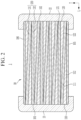
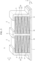
- FIG. 1 is a view showing a multilayer capacitor according to a first embodiment
- FIG. 2 is a longitudinal cross-sectional view taken along line I-I' of the multilayer capacitor of FIG. 1 .
- the multilayer capacitor 1 includes the body 10, the first external electrode 21, and the second external electrode 22.
- the body 10 has a predetermined volume.
- the body 10 may include a first internal electrode 110, a second internal electrode 120, and a dielectric layer 130.
- the first external electrode 21 may be connected to the first internal electrode 110.
- the first external electrode 21 may be connected to an end of the first internal electrode 110 toward the first end surface 101.
- the first external electrode 21 may be connected to the first internal electrode 110 on the first end surface 101 of the body 10.
- the first external electrode 21 may be made of a conductive material.
- the first external electrode 21 may be made of silver (Ag), palladium (Pd), gold (Au), platinum (Pt), nickel (Ni), copper (Cu), tin (Sn), tungsten (W), titanium (Ti), or an alloy thereof.
- the second external electrode 22 may be connected to the second internal electrode 120.
- the second external electrode 22 may be connected to an end of the second internal electrode 120 toward the second end surface 102.
- the second external electrode 22 may be connected to the second internal electrode 120 on the second end surface 102 of the body 10.
- the second external electrode 22 may be made of the conductive material.
- the second external electrode 22 may be made of silver (Ag), palladium (Pd), gold (Au), platinum (Pt), nickel (Ni), copper (Cu), tin (Sn), tungsten (W), titanium (Ti), or an alloy thereof.
- the first internal electrode 110 and the second internal electrode 120 may be stacked on each other in the thickness direction T.
- the first and second internal electrodes 110 and 120 may be alternately stacked on each other while being spaced apart from each other with the dielectric layer 130 interposed therebetween.
- the first internal electrode 110 and the second internal electrode 120 may be made of a conductive material.
- the first internal electrode 110 or the second internal electrode 120 may be made of silver (Ag), palladium (Pd), gold (Au), platinum (Pt), nickel (Ni), copper (Cu), tin (Sn), tungsten (W), titanium (Ti), molybdenum (Mo), tantalum (Ta), or an alloy thereof.
- the above-described material of the first internal electrode 110 or the second internal electrode 120 may be exemplary, and the first internal electrode 110 or the second internal electrode 120 may use another conductive material.
- the material of the first internal electrode 110 and the material of the second internal electrode 120 may be the same as each other or different from each other.
- An end of the first internal electrode 110 toward the second end surface 102 may be thinner than its end toward the first end surface 101.
- the first internal electrode 110 may have a part having an inclined plane and becoming thicker as closer to the first external electrode 21.
- the first internal electrode 110 may be thinner from the first end surface 101 to the second end surface 102.
- An upper surface 111 of the first internal electrode 110 may be inclined downward in the length direction L from the first end surface 101 to the second end surface 102. Accordingly, a cross section of the first internal electrode 110 in the thickness direction T and the length direction L may have a triangular shape.
- the upper surface 111 and lower surface 112 of the first internal electrode 110 opposing each other in the thickness direction T may have different shapes from each other.
- the lower surface 112 of the first internal electrode 110 may be a horizontal plane perpendicular to the thickness direction T. Accordingly, the cross section of the first internal electrode 110 in the thickness direction T and the length direction L may have a right-triangular shape.
- An end of the second internal electrode 120 toward the first end surface 101 may be thinner than its end toward the second end surface 102.
- the second internal electrode 120 may have a part having an inclined plane and becoming thicker as closer to the second external electrode 22.
- the second internal electrode 120 may be thinner from the second end surface 102 to the first end surface 101.
- the end of the second internal electrode 120 toward the second end surface 102 may have a thickness corresponding to that of the end of the first internal electrode 110 toward the first end surface 101.
- a lower surface 122 of the second internal electrode 122 may be inclined upward in the length direction L from the second end surface 102 to the first end surface 101. Accordingly, a cross section of the second internal electrode 120 in the thickness direction T and the length direction L may have a triangular shape.
- the lower surface 122 of the second internal electrode 120 may have an inclination corresponding to that of the upper surface 111 of the first internal electrode 110.
- the upper surface 121 and lower surface 122 of the second internal electrode 120 opposing each other in the thickness direction T may have different shapes from each other.
- the upper surface 121 of the second internal electrode 120 may be a horizontal plane perpendicular to the thickness direction T. Accordingly, the cross section of the second internal electrode 120 in the thickness direction T and the length direction L may have a right-triangular shape.
- a cross-sectional shape of the second internal electrode 120 may be point-symmetrical to the cross-sectional shape of the first internal electrode 110 based on their cross sections in the thickness direction T and the length direction L.
- the dielectric layer 130 may be disposed between the first internal electrode 110 and the second internal electrode 120.
- the dielectric layer 130 may include a first dielectric layer 131 and a second dielectric layer 132.
- the first dielectric layer 131 may be disposed between the upper surface 111 of the first internal electrode 110 and the lower surface 122 of the second internal electrode 120 opposing each other in the thickness direction T.
- the first dielectric layer 131 may be inclined downward in the length direction L from the first end surface 101 to the second end surface 102.
- An upper surface of the first dielectric layer 131 may be inclined downward to the second end surface 102 to correspond to the lower surface 122 of the second internal electrode 120.
- a lower surface of the first dielectric layer 131 may be inclined downward to the second end surface 102 to correspond to the upper surface 111 of the first internal electrode 110.
- the first dielectric layer 131 may have a uniform thickness in the length direction L.
- the second dielectric layer 132 may be disposed between the lower surface 112 of the first internal electrode 110 and the upper surface 121 of the second internal electrode 120 opposing each other in the thickness direction T.
- the second dielectric layer 132 may be horizontal to be parallel to the length direction L.
- An upper surface of the second dielectric layer 132 may be a horizontal plane corresponding to the lower surface 112 of the first internal electrode 110.
- a lower surface of the second dielectric layer 132 may be a horizontal plane corresponding to the upper surface 121 of the second internal electrode 120.
- the second dielectric layer 132 may have a uniform thickness in the length direction L.
- the first internal electrode 110 may become thinner toward the second end surface 102 of the body 10, and have one end sharp and extremely thin toward the second end surface 102. Accordingly, when the second external electrode 22 is connected to the second internal electrode 120, one end of the first internal electrode 110 toward the second end surface 102 may be maintained to be electrically short-circuited from the second external electrode 22 even in case of being disposed adjacent to the second end surface 102 of the body 10.
- the second internal electrode 120 may become thinner toward the first end surface 101 of the body 10, and have one end sharp and extremely thin toward the first end surface 101. Accordingly, when the first external electrode 21 is connected to the first internal electrode 110, one end of the second internal electrode 120 toward the first end surface 101 may be maintained to be electrically short-circuited from the first external electrode 21 even in case of being disposed adjacent to the first end surface 101 of the body 10.
- the body 10 of the multilayer capacitor 1 may be thin in comparison to the number of first internal electrodes 110 and second internal electrodes 120 stacked on each other.
- one unit section may refer to one first internal electrode 110, one second internal electrode 120, one first dielectric layer 131 and one second dielectric layer 132 in thickness direction T.
- a thickness of one unit section may be less than a sum of the thicknesses of one end of the first internal electrode 110 toward the first end surface 101, one end of the second internal electrode 120 toward the second end surface 102, the first dielectric layer 131, and the second dielectric layer 132.
- FIG. 3 is a cutaway perspective view of a multilayer capacitor according to a second embodiment.
- the substrate 9 may have a predetermined area.
- the substrate 9 may be made of an insulating material.
- the substrate 9 may be made of a metal material, a ceramic material, a glass material, or the like.
- the substrate 9 may be a silicon wafer or the like.
- the body 10 may be disposed on an upper surface of the substrate 9.
- the body 10 may include a first internal electrode 110, a second internal electrode 120, and a dielectric layer 130.
- the first internal electrode 110, the second internal electrode 120, and the dielectric layer 130 may correspond to those of the multilayer capacitor 1 according to the above-described first embodiment, and the description thus omits redundant descriptions thereof.
- the first external electrode 21 may be connected to the first internal electrode 110.
- the second external electrode 22 may be connected to the second internal electrode 120.
- the first internal electrode 21 or the second internal electrode 22 may correspond to those of the multilayer capacitor 1 according to the above-described first embodiment, and the description thus omits redundant descriptions thereof.
- FIG. 4 is a cutaway perspective view of a multilayer capacitor according to a third embodiment.
- the multilayer capacitor 1b may include a body 10, a first external electrode 21, and a second external electrode 22.
- the body 10 may include a first body 11 and a second body 12.
- the first body 11 and the second body 12 may respectively correspond to the body 10 described above with reference to FIGS. 1 and 2 , and the description thus omits redundant descriptions thereof.
- the first body 11 and the second body 12 may be disposed adjacent to each other.
- the second internal electrode 120 of the first body 11 and the second internal electrode 120 of the second body 12 may be connected to the second external electrode 22.
- the pair of first external electrodes 21 may be provided. Each of the first external electrodes 21 may oppose the second external electrode 22 in the length direction L while having the first body 11 or the second body 12 interposed therebetween.
- Each of the pair of first external electrodes 21 may be connected to the first internal electrode 110 of the first body 11 or the first internal electrode 110 of the second body 12.
- FIG. 5 is a cutaway perspective view of a multilayer capacitor according to a fourth embodiment.
- the multilayer capacitor 1c may include a substrate 9, a body 10, a first external electrode 21, and a second external electrode 22.
- the substrate 9 may have a predetermined area.
- the substrate 9 may be made of an insulating material.
- the substrate 9 may be made of a metal material, a ceramic material, a glass material, or the like.
- the substrate 9 may be a silicon wafer or the like.
- the body 10 may be disposed on an upper surface of the substrate 9.
- the body 10 may include a first body 11 and a second body 12.
- the first body 11 and the second body 12 may respectively correspond to the body 10 described above with reference to FIGS. 1 and 2 , and the description thus omits redundant descriptions thereof.
- the first body 11 and the second body 12 may be disposed adjacent to each other.
- the second internal electrode 120 of the first body 11 and the second internal electrode 120 of the second body 12 may be connected to the second external electrode 22.
- the pair of first external electrodes 21 may be provided. Each of the first external electrodes 21 may oppose the second external electrode 22 in the length direction L while having the first body 11 or the second body 12 interposed therebetween. Each of the pair of first external electrodes 21 may be connected to the first internal electrode 110 of the first body 11 or the first internal electrode 110 of the second body 12.
- FIG. 6 is a cutaway perspective view of a multilayer capacitor according to a fifth embodiment.
- the multilayer capacitor 1d may include a body 10, a first external electrode 21, and a second external electrode 22.
- the body 10 may include a first body 11 and a second body 12.
- the first body 11 and the second body 12 may respectively correspond to the body 10 described above with reference to FIGS. 1 and 2 , and the description thus omits redundant descriptions thereof.
- the first body 11 and the second body 12 may be disposed adjacent to each other.
- the first internal electrode 110 of the first body 11 and the first internal electrode 110 of the second body 12 may be connected to the first external electrode 21.
- the pair of second external electrodes 22 may be provided. Each of the second external electrodes 22 may oppose the first external electrode 21 in the length direction L while having the first body 11 or the second body 12 interposed therebetween.
- Each of the pair of second external electrodes 22 may be connected to the second internal electrode 120 of the first body 11 or the second internal electrode 120 of the second body 12.
- FIG. 7 is a cutaway perspective view of a multilayer capacitor according to a sixth embodiment.
- the multilayer capacitor 1e may include a substrate 9, a body 10, a first external electrode 21, and a second external electrode 22.
- the substrate 9 may have a predetermined area.
- the substrate 9 may be made of an insulating material.
- the substrate 9 may be made of a metal material, a ceramic material, a glass material, or the like.
- the substrate 9 may be a silicon wafer or the like.
- the body 10 may be disposed on an upper surface of the substrate 9.
- the body 10 may include a first body 11 and a second body 12.
- the first body 11 and the second body 12 may respectively correspond to the body 10 described above with reference to FIGS. 1 and 2 , and the description thus omits redundant descriptions thereof.
- the first body 11 and the second body 12 may be disposed adjacent to each other.
- the first internal electrode 110 of the first body 11 and the first internal electrode 110 of the second body 12 may be connected to the first external electrode 21.
- the pair of second external electrodes 22 may be provided. Each of the second external electrodes 22 may oppose the first external electrode 21 in the length direction L while having the first body 11 or the second body 12 interposed therebetween. Each of the pair of second external electrodes 22 may be connected to the second internal electrode 120 of the first body 11 or the second internal electrode 120 of the second body 12.
- FIG. 8 is a view showing a body according to the second embodiment.
- the body 10a according to the second embodiment may include a first internal electrode 110, a second internal electrode 120, and a dielectric layer 130.
- the first internal electrode 110 and the second internal electrode 120 may be alternately stacked on each other while being spaced apart from each other with the dielectric layer 130 interposed therebetween.
- the first internal electrode 110 and the second internal electrode 120 may be made of a conductive material.
- An end of the first internal electrode 110 toward the second end surface 102 may be thinner than its end toward the first end surface 101.
- the first internal electrode 110 may have a part having an inclined plane in at least a partial region thereof and becoming thicker as closer to the first end surface 101.
- the upper surface 111 and lower surface 112 of the first internal electrode 110 opposing each other in the thickness direction T may have different shapes from each other.
- One end of the first internal electrode 110 toward the second end surface 102 may be spaced apart from the second end surface 102 toward the first end surface 101 by a predetermined distance.
- the upper surface 111 of the first internal electrode 110 may include a first inclined part 111a and a first horizontal part 111b.
- the first inclined part 111a may be disposed in a region of the first internal electrode 110 toward the second end surface 102.
- the first inclined part 111a may be inclined downward toward the second end surface 102. Accordingly, the region of the first internal electrode 110 toward the second end surface 102 may become thinner toward the second end surface 102.
- the first inclined part 111a may be disposed in a region OL where the first internal electrode 110 opposes the second internal electrode 120 in the thickness direction T.
- a cross section of the region of the first internal electrode 110 toward the second end surface 102 in the thickness direction T and the length direction L may have a triangular shape.
- the first horizontal part 111b may be disposed in a region of the first internal electrode 110 toward the first end surface 101.
- the first horizontal part 111b may be disposed outside the region OL where the first internal electrode 110 opposes the second internal electrode 120 in the thickness direction T.
- the first horizontal part 111b may be a horizontal plane perpendicular to the thickness direction T.
- the lower surface 112 of the first internal electrode 110 may be a horizontal plane perpendicular to the thickness direction T. Accordingly, a cross section of the region of the first internal electrode 110 toward the second end surface 102 in the thickness direction T and the length direction L may have a right-triangular shape. The region of the first internal electrode 110 toward the first end surface 101 may have uniform upper and lower thicknesses in the length direction L.
- An end of the second internal electrode 120 toward the first end surface 101 may be thinner than its end toward the second end surface 102.
- the second internal electrode 120 may have a part having an inclined plane in at least a partial region thereof and becoming thicker as closer to the second end surface 102.
- the upper surface 121 and lower surface 122 of the second internal electrode 120 opposing each other in the thickness direction T may have different shapes from each other.
- One end of the second internal electrode 120 toward the first end surface 101 may be spaced apart from the first end surface 101 toward the second end surface 102 by a predetermined distance.
- the lower surface 122 of the second internal electrode 120 may include a second inclined part 122a and a second horizontal part 122b.
- the second inclined part 122a may be disposed in a region of the second internal electrode 120 toward the first end surface 101.
- the second inclined part 122a may be inclined upward toward the first end surface 101. Accordingly, the region of the second internal electrode 120 toward the first end surface 101 may become thinner toward the first end surface 101.
- a cross section of the region of the second internal electrode 120 toward the first end surface 102 in the thickness direction T and the length direction L may have a triangular shape.
- the second inclined part 122a may be disposed in the region OL where the second internal electrode 120 opposes the first internal electrode 110 in the thickness direction T.
- the second inclined part 122a may be aligned with the first inclined part 111a in the thickness direction T.
- An inclination of the second inclined part 122a may correspond to an inclination of the first inclined part 111a.
- the second horizontal part 122b may be disposed in a region of the second internal electrode 120 toward the second end surface 102.
- the second horizontal part 122b may be disposed outside the region OL where the second internal electrode 120 opposes the first internal electrode 110 in the thickness direction T.
- the second horizontal part 122b may be a horizontal plane perpendicular to the thickness direction T.
- the upper surface 121 of the second internal electrode 120 may be a horizontal plane perpendicular to the thickness direction T. Accordingly, a cross section of the region of the second internal electrode 120 toward the first end surface 101 in the thickness direction T and the length direction L may have a right-triangular shape. The region of the second internal electrode 120 toward the second end surface 102 may have a uniform thickness in the length direction L.
- the dielectric layer 130 may be disposed between the first internal electrode 110 and the second internal electrode 120.
- the dielectric layer 130 may include a first dielectric layer 131 and a second dielectric layer 132.
- the first dielectric layer 131 may be disposed between the upper surface 111 of the first internal electrode 110 and the lower surface 122 of the second internal electrode 120 opposing each other in the thickness direction T.
- the first dielectric layer 131 may be disposed between the first inclined part 111a of the first internal electrode 110 and the second inclined part 122a of the second internal electrode 120.
- the first dielectric layer 131 may be inclined downward toward the second end surface 102 in the length direction L.
- the upper surface of the first dielectric layer 131 may be inclined downward toward the second end surface 102 to correspond to the second inclined part 122a.
- the lower surface of the first dielectric layer 131 may be inclined downward toward the second end surface 102 to correspond to the first inclined part 111a.
- the first dielectric layer 131 may have a uniform thickness in the thickness direction T along the length direction L.
- the second dielectric layer 132 may be disposed between the lower surface 112 of the first internal electrode 110 and the upper surface 121 of the second internal electrode 120 opposing each other in the thickness direction T.
- the second dielectric layer 132 may be horizontal to be parallel to the length direction L.
- An upper surface of the second dielectric layer 132 may be a horizontal plane corresponding to the lower surface 112 of the first internal electrode 112.
- a lower surface of the second dielectric layer 132 may be a horizontal plane corresponding to the upper surface 121 of the second internal electrode 120.
- the second dielectric layer 132 may have a uniform thickness in the thickness direction T along the length direction L.
- the first external electrode 21 may be connected to the region of the first internal electrode 110 toward the first end surface 101.
- the first external electrode 21 may be connected to the first internal electrode 110 on the first end surface 101 of the body 10.
- the first external electrode 21 may be made of a conductive material.
- the second external electrode 22 may be connected to the region of the second internal electrode 120 toward the second end surface 102.
- the second external electrode 22 may be connected to the second internal electrode 120 on the second end surface 102 of the body 10.
- the first external electrode 21 may be made of a conductive material.
- one end of the first internal electrode 110 may be sharp and extremely thin toward the second end surface 102. Accordingly, the first internal electrode 110 may be effectively maintained to be electrically short-circuited from the second external electrode 22.
- one end of the second internal electrode 120 may be sharp and extremely thin toward the first end surface 101. Accordingly, the second internal electrode 120 may be effectively maintained to be electrically short-circuited from the first external electrode 21.
- the body 10a according to the second embodiment may be thin in comparison to the number of first internal electrodes 110 and second internal electrodes 120 stacked on each other.
- the body 10a according to the second embodiment may be applied to the multilayer capacitor 1, 1a, 1b, 1c, 1d and 1e according to the first to sixth embodiments described above with reference to FIGS. 1 to 7 .
- the multilayer capacitors 1b, 1c, 1d, and 1e according to the third to sixth embodiments may respectively use one body 10 described above with reference to FIG. 2 and one body 10a according to the second embodiment.
- a unit process section U.P. refers to a section where the first internal electrode 110 and the second internal electrode 120 are stacked on each other in the length direction L to produce one body 10 or 10a.
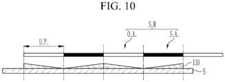
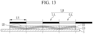
- FIGS. 9 to 14 are views showing a manufacturing method of the multilayer capacitor according to the first embodiment.
- a shadow mask S.M for depositing the first internal electrode 110 may be aligned and disposed on the top of a substrate S.
- the substrate S may have the dielectric layer 130 formed on its upper surface, or its upper surface may be exposed upward without the dielectric layer 130.
- the shadow mask S.M may include at least one shield region S.A. and at least one open region O.A. arranged in the length direction L.
- the shield region S.A. and the open region O.A. may be disposed alternately with each other.
- a length of the shield region S.A. in the length direction L and a length of the open region O.A. in the length direction L may correspond to a length of the unit process section U.P.
- the rear end of the shield region S.A. and the rear end of the open region O.A. may be vertically aligned with the rear end of the unit process section U.P.
- the dielectric layer 130 may be formed.
- the dielectric layer may be formed to a uniform thickness through a deposition process. Accordingly, the first dielectric layer 131 may be formed on the first internal electrode 110.
- the shadow mask S.M for depositing the second internal electrode 120 may be aligned and disposed on the top of the substrate S.
- the shield region S.A. may be disposed in a region where the open region O.A. is disposed in a step of depositing the first internal electrode 110, and the open region O.A. may be disposed in a region where the shield region S.A. is disposed in the step of depositing the first internal electrode 110.
- deposition of the second internal electrode 120 may be performed while the shadow mask S.M is relatively moved forward with respect to the substrate S.
- the deposition of the second internal electrode 120 may be performed while the shadow mask S.M is relatively moved by the length of the unit process section U.P.
- the second internal electrode 120 may be deposited to have the inclined lower surface 122.
- the upper surface 121 of the second internal electrode 120 may have the horizontal plane shape.
- One second internal electrode 120 may be formed for each unit process section U.P.
- the dielectric layer 130 may be formed.
- the dielectric layer 130 may be formed to a uniform thickness through the deposition process. Accordingly, the second dielectric layer 132 may be formed on the second internal electrode 120.
- the body 10 in which the first internal electrode 110 and the second internal electrode 120 are vertically stacked on each other may be manufactured in each unit process section U.P. when the deposition of the first internal electrode 110, the formation of the dielectric layer 130, the deposition of the second internal electrode 120, and the formation of the dielectric layer 130, as described above, are repeated two or more times.
- manufacturing of the multilayer capacitor 1 may be completed when the first external electrode 21 and the second external electrode 22 are respectively connected to the first internal electrode 110 and the second internal electrode 120.
- the body 10 may be manufactured through the deposition process. Accordingly, it is possible to manufacture the multilayer capacitor 1, 1a, 1b, 1c, 1d, or 1e in which the first internal electrode 110 and the second internal electrode 120 each having a finer structure are stacked on each other at high density.
- FIGS. 15 and 16 are views showing a manufacturing method of the multilayer capacitor according to the second embodiment.
- the shadow mask S.M for depositing the first internal electrode 110 may be aligned and disposed on the top of the substrate S, and deposition of the first internal electrode 110 may then be performed while the shadow mask S.M is relatively moved forward with respect to the substrate S.
- the dielectric layer 130 may then be formed. Detailed processes are the same as those of FIGS. 9 to 11 , and the description thus omits redundant descriptions thereof.
- deposition of the second internal electrode 120 may be performed while the shadow mask S.M is relatively moved backward with respect to the substrate S.
- the deposition of the second internal electrode 120 may be performed while the shadow mask S.M is relatively moved by the length of the unit process section U.P.
- One second internal electrode 120 may be formed for each unit process section U.P.
- the dielectric layer 130 may then be formed.
- a method of forming the dielectric layer 130 is the same as that of FIG. 14 , and the description thus omits redundant description thereof.
- the body 10 in which the first internal electrode 110 and the second internal electrode 120 are vertically stacked on each other may be manufactured in each unit process section U.P. when the deposition of the first internal electrode 110, the formation of the dielectric layer 130, the deposition of the second internal electrode 120, and the formation of the dielectric layer 130, as described above, are repeated two or more times.
- manufacturing of the multilayer capacitor 1, 1a, 1b, 1c, 1d, or 1e may be completed when the first external electrode 21 and the second external electrode 22 are respectively connected to the first internal electrode 110 and the second internal electrode 120.
- the body 10 of the multilayer capacitor 1, 1a, 1b, 1c, 1d, or 1e may be manufactured through the deposition process. Accordingly, it is possible to manufacture the multilayer capacitor 1, 1a, 1b, 1c, 1d, or 1e in which the first internal electrode 110 and the second internal electrode 120 each having a finer structure are stacked on each other at high density.
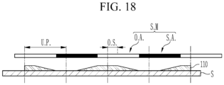
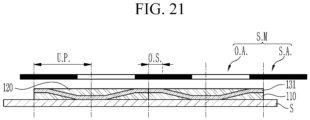
- FIGS. 17 to 22 are views showing a manufacturing method of the multilayer capacitor according to the third embodiment.
- the shadow mask S.M for depositing the first internal electrode 110 may be aligned and disposed on the top of the substrate S.
- the substrate S may have the dielectric layer 130 formed on its upper surface, or its upper surface may be exposed upward without the dielectric layer 130.
- the shadow mask S.M may include at least one shield region S.A. and at least one open region O.A. arranged in the length direction L.
- the shield region S.A. and the open region O.A. may be disposed alternately with each other.
- a length of the shield region S.A. in the length direction L and a length of the open region O.A. in the length direction L may each correspond to a length of the unit process section U.P.
- the and the open region O.A. may be disposed by being moved forward, which is a relative movement direction of the shadow mask S.M, by an offset distance O.S. from a boundary of the unit process section U.P.
- the offset distance O.S. may be less than half the length of the unit process section U.P.
- deposition of the first internal electrode 110 may be performed while the shadow mask S.M is moved relatively forward with respect to the substrate S. Relative forward movement may indicate that the shadow mask S.M is moved forward, the substrate S is moved backward, or the shadow mask S.M is moved forward while the substrate S is moved backward.
- the deposition of the first internal electrode 110 may be performed while the shadow mask S.M is moved by a distance shorter than the length of the unit process section U.P.
- the boundary between the shield region S.A. and the open region O.A. may be disposed at a point spaced by a predetermined distance backward from the boundary of the unit process section U.P.
- a movement distance of the shadow mask S.M. may have a value obtained by subtracting twice the offset distance O.S. from the length of the unit process section U.P.
- the upper surface 111 of the first internal electrode 110 may be deposited to have the first inclined part 111a, the first horizontal part 111b, and have an inclination in a partial region.
- the first internal electrode 110 may not be deposited in a section where the first inclined parts 111a oppose each other.
- One first internal electrode 110 may be formed for each unit process section U.P.
- the dielectric layer 130 may be formed.
- the dielectric layer may be formed to a uniform thickness through the deposition process. Accordingly, the first dielectric layer 131 may be formed on the first internal electrode 110.
- the shadow mask S.M for depositing the second internal electrode 120 may be aligned and disposed on the top of the substrate S.
- the shield region S.A. may be disposed in a region where the open region O.A. is disposed in a step of depositing the first internal electrode 110, and the open region O.A. may be disposed in a region where the shield region S.A. is disposed in the step of depositing the first internal electrode 110.
- the front end of the shield region S.A. and the front end of the open region O.A. may be disposed while being moved forward by the offset distance O.S. from the boundary of the unit process section U.P.
- deposition of the second internal electrode 120 may be performed while the shadow mask S.M is relatively moved forward with respect to the substrate S.
- the deposition of the second internal electrode 120 may be performed while the shadow mask S.M is relatively moved by the distance shorter than the length of the unit process section U.P.
- the boundary between the shield region S.A. and the open region O.A. may be disposed at a point spaced by a predetermined distance backward from the boundary of the unit process section U.P.
- a movement distance of the shadow mask S.M. may have a value obtained by subtracting twice the offset distance O.S. from the length of the unit process section U.P.
- the lower surface 122 of the second internal electrode 120 may be deposited to have the second inclined part 122a, the second horizontal part 122b, and have an inclination in a partial region.
- One second internal electrode 120 may be formed for each unit process section U.P.
- the second internal electrode 120 may not be deposited in a section where the second inclined parts 122a oppose each other.
- the dielectric layer 130 may be formed.
- the dielectric layer 130 may be formed to a uniform thickness through the deposition process. Accordingly, the second dielectric layer 132 may be formed on the second internal electrode 120.
- the shadow mask S.M for depositing the second internal electrode 120 may be disposed at the same position as when the deposition of the first internal electrode 110 begins.
- the deposition of the second internal electrode 120 may be performed while the shadow mask S.M is relatively moved backward with respect to the substrate S.
- the body 10 or 10a in which the first internal electrode 110 and the second internal electrode 120 are vertically stacked on each other may be manufactured in each unit process section U.P. when the deposition of the first internal electrode 110, the formation of the dielectric layer 130, the deposition of the second internal electrode 120, and the formation of the dielectric layer 130, as described above, are repeated two or more times.
- manufacturing of the multilayer capacitor 1a, 1b, 1c, 1d, or 1e may be completed when the first external electrode 21 and the second external electrode 22 are respectively connected to the first internal electrode 110 and the second internal electrode 120.
- the body 10 or 10a of the multilayer capacitor 1a, 1b, 1c, 1d, or 1e may be manufactured through the deposition process. Accordingly, it is possible to manufacture the multilayer capacitor 1a, 1b, 1c, 1d, or 1e in which the first internal electrode 110 and the second internal electrode 120 each having a finer structure are stacked on each other at high density.
- the body 10a according to the second embodiment may be manufactured through the deposition process.
- the body 10 described above may be manufactured in the multilayer capacitor 1 according to the first embodiment by removing the region where the first horizontal part 111b and the second horizontal part 122b are formed.
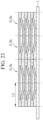
- FIGS. 23 to 25 are views showing a manufacturing method of the multilayer capacitor according to the fourth embodiment.
- the plurality of bodies 10 or 10a may be provided.
- the plurality of bodies 10 or 10a may be connected to each other.
- the plurality of bodies 10 or 10a may be disposed on an upper surface of the substrate S.
- the bodies 10 or 10a may each be manufactured by the manufacturing method of the multilayer capacitor according to the third embodiment, and disposed in the unit process section U.P.
- a groove G may be formed.
- the groove G may be formed in a region where the bodies 10 or 10a are connected to each other to separate the bodies 10 or 10a from each other.
- the groove G may include a region where the boundary of the unit process section U.P. is disposed.
- a depth of the groove G may correspond to a thickness of the body 10 or 10a.
- the groove G may be formed through a cutting process using a laser or a mechanical cutter. Alternatively, the groove G may be formed through an etching process.
- the first external electrode 21 and the second external electrode 22 may be formed in each of the bodies 10 or 10a.
- the first external electrode 21 may be connected to the first internal electrode 110 of the body 10 or 10a
- the second external electrode 22 may be connected to the second internal electrode 120 of the body 10 or 10a.
- the first external electrode 21 or the second external electrode 22 may be formed through the deposition process.
- a mask may be used for the deposition of the first external electrode 21 or the second external electrode 22.
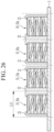
- FIG. 26 is a view showing a manufacturing method of the multilayer capacitor according to the fifth embodiment.
- the groove G may be formed in the plurality of bodies 10 or 10a.
- the formation of the plurality of bodies 10 or 10a and the groove G is the same as the manufacturing method of the multilayer capacitor according to the fourth embodiment, and the description thus omits redundant descriptions thereof.
- the first external electrode 21 may be formed between the bodies 10 or 10a adjacent to each other, and each side of the first external electrode 21 may thus be connected to the first internal electrode 110 of the adjacent body 10 or 10a.
- the second external electrode 22 may be formed on a side of the body 10 or 10a that is opposite to its side where the first external electrode 21 is formed.
- the second external electrode 22 may be connected to the second internal electrode 120 of the body 10 or 10a.
Landscapes
- Engineering & Computer Science (AREA)
- Power Engineering (AREA)
- Manufacturing & Machinery (AREA)
- Microelectronics & Electronic Packaging (AREA)
- Chemical & Material Sciences (AREA)
- Ceramic Engineering (AREA)
- Inorganic Chemistry (AREA)
- Materials Engineering (AREA)
- Fixed Capacitors And Capacitor Manufacturing Machines (AREA)
- Ceramic Capacitors (AREA)
Abstract

Description
- The present disclosure relates to a multilayer capacitor and a manufacturing method of the same.
- An electronic component used in an electronic device may include a capacitor, an inductor, a piezoelectric element, a varistor, or a thermistor. The multilayer capacitor among these ceramic electronic components may be used in various electronic devices because the capacitor is small, implements high capacitance, and is easily mounted.
- For example, the multilayer capacitor may be used as a chip-type capacitor serving to charge or discharge electricity by being mounted on a substrate of various electronic products such as a video device such as a liquid crystal display (LCD), a plasma display panel (PDP), or an organic light-emitting diode (OLED) display, a computer, a personal portable terminal, and a smart phone.
- In accordance with a recent trend that the electronic product becomes smaller and thinner, there is an increasing demand for a multilayer capacitor which is thinner than an existing multilayer capacitor.
- Embodiments of the present disclosure provide a multilayer capacitor in which several layers of first internal electrodes and second internal electrodes are stacked on each other, while maintaining its smaller thickness, and a manufacturing method of the same.
- Embodiments of the present disclosure also provide a multilayer capacitor in which a first internal electrode and a second internal electrode are respectively connected to a first external electrode and a second external electrode, and effectively short-circuited from the second external electrode and the first internal electrode respectively, and a manufacturing method of the same.
- According to an embodiment, a multilayer capacitor includes: a body including a dielectric layer, and first and second internal electrodes stacked on each other in a thickness direction of the capacitor while being spaced apart from each other with the dielectric layer interposed therebetween; a first external electrode connected to the first internal electrode; and a second external electrode spaced apart from the first external electrode in a length direction of the capacitor that is perpendicular to the thickness direction, and connected to the second internal electrode. One of the first internal electrode and the second internal electrode has a horizontal plane perpendicular to the thickness direction and an inclined plane inclined with respect to the horizontal plane in at least a partial region thereof.
- An upper surface of the first internal electrode may be inclined downward in the length direction from the first external electrode toward the second external electrode.
- A lower surface of the second internal electrode may be inclined upward in the length direction from the second external electrode toward the first external electrode.
- The first internal electrode and the second internal electrode may be point-symmetrical to each other based on their cross sections in the thickness direction and the length direction.
- An upper surface of the first internal electrode may include a first inclined part disposed in a region where the first internal electrode opposes the second internal electrode in the thickness direction, and a first horizontal part disposed outside the region where the first internal electrode opposes the second internal electrode in the thickness direction.
- A lower surface of the second internal electrode may include a second inclined part disposed in a region where the second internal electrode opposes the first internal electrode in the thickness direction, and a second horizontal part disposed outside the region where the second internal electrode opposes the first internal electrode in the thickness direction.
- The dielectric layer may include a first dielectric layer disposed between an upper surface of the first internal electrode and a lower surface of the second internal electrode opposing each other in the thickness direction, and inclined in the length direction, and a second dielectric layer disposed between a lower surface of the first internal electrode and an upper surface of the second internal electrode opposing each other in the thickness direction, and parallel to the length direction.
- The first dielectric layer or the second dielectric layer may have a uniform thickness between the first internal electrode and the second internal electrode in the length direction.
- The body may include a first body and a second body adjacent to each other and respectively connected to the second external electrode, and each of the pair of first external electrodes may oppose the second external electrode while having the first body or the second body interposed therebetween.
- The body may include a first body and a second body adjacent to each other and respectively connected to the first external electrode, and each of the pair of second external electrodes may oppose the first external electrode while having the first body or the second body interposed therebetween.
- Another of the first internal electrode and the second internal electrode may have a horizontal plane perpendicular to the thickness direction and an inclined plane inclined with respect to the horizontal plane in at least a partial region thereof.
- The capacitor may further include a substrate on which the body is disposed.
- The body may include another dielectric layer in contact with the substrate.
- According to another embodiment, a manufacturing method of a multilayer capacitor includes: forming a first internal electrode having an inclination in at least a partial region thereof by disposing a shadow mask having a shield region and an open region, which are arranged in front and back, to be vertically aligned on a top of a substrate, and then performing a deposition process of the first internal electrode while relatively moving the shadow mask with respect to the substrate forward or backward; forming a dielectric layer on the first internal electrode; forming a second internal electrode having an inclination in at least a partial region thereof by disposing the shadow mask to be vertically aligned on the top of the substrate, and then performing a deposition process of the second internal electrode while relatively moving the shadow mask with respect to the substrate forward or backward; and forming another dielectric layer on the second internal electrode.
- Lengths of the shield region and the open region which are arranged in front and back may each correspond to a length of a unit process section which is a section where one body formed by stacking the first internal electrode and the second internal electrode on each other is manufactured.
- The shadow mask may be relatively moved by the length of the unit process section in a process of performing the deposition process to form the first internal electrode or the second internal electrode.
- A position where the shadow mask is vertically aligned on the top of the substrate to form the first internal electrode or the second internal electrode may be a position where a boundary between the shield region and the open region is moved by an offset distance from a boundary of the unit process section in a relative movement direction of the shadow mask with respect to the substrate.
- According to another embodiment, a multilayer capacitor includes: a body including a dielectric layer, and first and second internal electrodes stacked on each other in a thickness direction of the capacitor while being spaced apart from each other with the dielectric layer interposed therebetween, the first internal electrode extending from a first end surface of the body and the second internal electrode extending from a second end surface of the body; a first external electrode disposed on the first end surface to connect to the first internal electrode; and a second external electrode spaced apart from the first external electrode in a length direction of the capacitor, and disposed on the second end surface to connect to the second internal electrode. One of the first internal electrode and the second internal electrode has an upper surface and a lower surface having different angles with respect to one of the first end surface and the second end surface.
- The embodiments of the present disclosure may provide the multilayer capacitor in which several layers of the first internal electrodes and the second internal electrodes are stacked on each other, while maintaining its smaller thickness, and the manufacturing method of the same.
- The embodiments of the present disclosure may also provide the multilayer capacitor in which the first internal electrode and the second internal electrode are respectively connected to the first external electrode and the second external electrode, and effectively short-circuited from the second external electrode and the first internal electrode respectively, and the manufacturing method of the same.
-
-
FIG. 1 is a view showing a multilayer capacitor according to a first embodiment. -
FIG. 2 is a longitudinal cross-sectional view taken along line I-I' of the multilayer capacitor ofFIG. 1 . -
FIG. 3 is a cutaway perspective view of a multilayer capacitor according to a second embodiment. -
FIG. 4 is a cutaway perspective view of a multilayer capacitor according to a third embodiment. -
FIG. 5 is a cutaway perspective view of a multilayer capacitor according to a fourth embodiment. -
FIG. 6 is a cutaway perspective view of a multilayer capacitor according to a fifth embodiment. -
FIG. 7 is a cutaway perspective view of a multilayer capacitor according to a sixth embodiment. -
FIG. 8 is a view showing a body according to the second embodiment. -
FIGS. 9 to 14 are views showing a manufacturing method of the multilayer capacitor according to the first embodiment. -
FIGS. 15 and16 are views showing a manufacturing method of the multilayer capacitor according to the second embodiment. -
FIGS. 17 to 22 are views showing a manufacturing method of the multilayer capacitor according to the third embodiment. -
FIGS. 23 to 25 are views showing a manufacturing method of the multilayer capacitor according to the fourth embodiment. -
FIG. 26 is a view showing a manufacturing method of the multilayer capacitor according to the fifth embodiment. - Hereinafter, embodiments of the present disclosure are described in detail with reference to the accompanying drawings so that those skilled in the art to which the present disclosure pertains may easily practice the present disclosure. A portion unrelated to the description is omitted in order to obviously describe the present disclosure, and the same or similar components are denoted by the same reference numeral throughout the specification. In addition, it is to be noted that some components shown in the accompanying drawings are exaggerated, omitted or schematically shown, and the size of each component does not exactly reflect its real size.
- It should be understood that the accompanying drawings are provided only to allow the embodiments of the present disclosure to be easily understood, and the spirit of the present disclosure is not limited by the accompanying drawings, and includes all the modifications, equivalents, and substitutions included in the spirit and scope of the present disclosure.
- Terms including ordinal numbers such as "first," "second," and the like, may be used to describe various components. However, these components are not limited by these terms. These terms are used only to distinguish one component from another component.
- In addition, when an element such as a layer, a film, a region or a substrate is referred to as being "on" or "above" another element, the element may be "directly on" another element or may have a third element interposed therebetween.
- On the contrary, when an element is referred to as being "directly on" another element, there is no third element interposed therebetween.
- In addition, when referred to as being "on" or "above" a reference element, an element may be disposed on or below the reference element, and may not necessarily be "on" or "above" the reference element in an opposite direction of gravity.
- It should be understood that terms "include" and "comprise" used in the specification specify the presence of features, numerals, steps, operations, components, parts, or combinations thereof, mentioned in the specification, and do not preclude the presence or addition of one or more other features, numerals, steps, operations, components, parts, or combinations thereof. Unless explicitly described to the contrary, "including" any component is to be understood to imply the inclusion of another element rather than the exclusion of another component.
- Further, throughout the specification, an expression "on the plane" may indicate a case where a target is viewed from the top, and an expression "on the cross section" may indicate a case where a cross section of a target taken along a vertical direction is viewed from its side.
- In addition, when it is mentioned that any component is "connected" to another component, it may not only indicate that two or more components are directly connected with each other, but also indicate that two or more components are connected with each other indirectly through still another component, may not only indicate that two or more components are physically connected with each other, but also indicate that two or more components are electrically connected with each other, or two or more components are a single entity although referred to by different names based on their positions or functions.
- Hereinafter, a thickness direction T refers to a direction in which components of a
multilayer capacitor - In addition, a length direction L and a width direction W refer to directions respectively disposed on a plane perpendicular to the thickness direction T, and orthogonal to each other.
- Here, the length direction L refers a direction in which a first
external electrode 21 and a secondexternal electrode 22 are spaced apart from each other. - In addition, a
first end surface 101 and asecond end surface 102 refer to surfaces opposing each other while being spaced apart from each other in the length direction L among outer surfaces of abody multilayer capacitor - In addition, a
first side surface 103 and asecond side surface 104 refer to surfaces perpendicularly crossing thefirst end surface 101 and thesecond end surface 102 and opposing each other in the width direction W. - In addition, a
top surface 105 and abottom surface 106 refer to surfaces opposing each other while being spaced apart from each other in the thickness direction T. -
FIG. 1 is a view showing a multilayer capacitor according to a first embodiment, andFIG. 2 is a longitudinal cross-sectional view taken along line I-I' of the multilayer capacitor ofFIG. 1 . - Referring to
FIGS. 1 and2 , themultilayer capacitor 1 according to an embodiment includes thebody 10, the firstexternal electrode 21, and the secondexternal electrode 22. - The
body 10 has a predetermined volume. - The
body 10 may include a firstinternal electrode 110, a secondinternal electrode 120, and adielectric layer 130. - The first
external electrode 21 may be connected to the firstinternal electrode 110. - The first
external electrode 21 may be connected to an end of the firstinternal electrode 110 toward thefirst end surface 101. - For example, the first
external electrode 21 may be connected to the firstinternal electrode 110 on thefirst end surface 101 of thebody 10. - The first
external electrode 21 may be made of a conductive material. - For example, the first
external electrode 21 may be made of silver (Ag), palladium (Pd), gold (Au), platinum (Pt), nickel (Ni), copper (Cu), tin (Sn), tungsten (W), titanium (Ti), or an alloy thereof. - The second
external electrode 22 may be connected to the secondinternal electrode 120. - The second
external electrode 22 may be connected to an end of the secondinternal electrode 120 toward thesecond end surface 102. - For example, the second
external electrode 22 may be connected to the secondinternal electrode 120 on thesecond end surface 102 of thebody 10. - The second
external electrode 22 may be made of the conductive material. - For example, the second
external electrode 22 may be made of silver (Ag), palladium (Pd), gold (Au), platinum (Pt), nickel (Ni), copper (Cu), tin (Sn), tungsten (W), titanium (Ti), or an alloy thereof. - The first
internal electrode 110 and the secondinternal electrode 120 may be stacked on each other in the thickness direction T. - The first and second
internal electrodes dielectric layer 130 interposed therebetween. - The first
internal electrode 110 and the secondinternal electrode 120 may be made of a conductive material. - The first
internal electrode 110 or the secondinternal electrode 120 may be made of silver (Ag), palladium (Pd), gold (Au), platinum (Pt), nickel (Ni), copper (Cu), tin (Sn), tungsten (W), titanium (Ti), molybdenum (Mo), tantalum (Ta), or an alloy thereof. The above-described material of the firstinternal electrode 110 or the secondinternal electrode 120 may be exemplary, and the firstinternal electrode 110 or the secondinternal electrode 120 may use another conductive material. The material of the firstinternal electrode 110 and the material of the secondinternal electrode 120 may be the same as each other or different from each other. - An end of the first
internal electrode 110 toward thesecond end surface 102 may be thinner than its end toward thefirst end surface 101. The firstinternal electrode 110 may have a part having an inclined plane and becoming thicker as closer to the firstexternal electrode 21. The firstinternal electrode 110 may be thinner from thefirst end surface 101 to thesecond end surface 102. Anupper surface 111 of the firstinternal electrode 110 may be inclined downward in the length direction L from thefirst end surface 101 to thesecond end surface 102. Accordingly, a cross section of the firstinternal electrode 110 in the thickness direction T and the length direction L may have a triangular shape. - The
upper surface 111 andlower surface 112 of the firstinternal electrode 110 opposing each other in the thickness direction T may have different shapes from each other. Thelower surface 112 of the firstinternal electrode 110 may be a horizontal plane perpendicular to the thickness direction T. Accordingly, the cross section of the firstinternal electrode 110 in the thickness direction T and the length direction L may have a right-triangular shape. - An end of the second
internal electrode 120 toward thefirst end surface 101 may be thinner than its end toward thesecond end surface 102. The secondinternal electrode 120 may have a part having an inclined plane and becoming thicker as closer to the secondexternal electrode 22. The secondinternal electrode 120 may be thinner from thesecond end surface 102 to thefirst end surface 101. The end of the secondinternal electrode 120 toward thesecond end surface 102 may have a thickness corresponding to that of the end of the firstinternal electrode 110 toward thefirst end surface 101. Alower surface 122 of the secondinternal electrode 122 may be inclined upward in the length direction L from thesecond end surface 102 to thefirst end surface 101. Accordingly, a cross section of the secondinternal electrode 120 in the thickness direction T and the length direction L may have a triangular shape. Thelower surface 122 of the secondinternal electrode 120 may have an inclination corresponding to that of theupper surface 111 of the firstinternal electrode 110. - The
upper surface 121 andlower surface 122 of the secondinternal electrode 120 opposing each other in the thickness direction T may have different shapes from each other. Theupper surface 121 of the secondinternal electrode 120 may be a horizontal plane perpendicular to the thickness direction T. Accordingly, the cross section of the secondinternal electrode 120 in the thickness direction T and the length direction L may have a right-triangular shape. A cross-sectional shape of the secondinternal electrode 120 may be point-symmetrical to the cross-sectional shape of the firstinternal electrode 110 based on their cross sections in the thickness direction T and the length direction L. - The
dielectric layer 130 may be disposed between the firstinternal electrode 110 and the secondinternal electrode 120. Thedielectric layer 130 may include a firstdielectric layer 131 and asecond dielectric layer 132. - The
first dielectric layer 131 may be disposed between theupper surface 111 of the firstinternal electrode 110 and thelower surface 122 of the secondinternal electrode 120 opposing each other in the thickness direction T. Thefirst dielectric layer 131 may be inclined downward in the length direction L from thefirst end surface 101 to thesecond end surface 102. An upper surface of thefirst dielectric layer 131 may be inclined downward to thesecond end surface 102 to correspond to thelower surface 122 of the secondinternal electrode 120. A lower surface of thefirst dielectric layer 131 may be inclined downward to thesecond end surface 102 to correspond to theupper surface 111 of the firstinternal electrode 110. Thefirst dielectric layer 131 may have a uniform thickness in the length direction L. - The
second dielectric layer 132 may be disposed between thelower surface 112 of the firstinternal electrode 110 and theupper surface 121 of the secondinternal electrode 120 opposing each other in the thickness direction T. Thesecond dielectric layer 132 may be horizontal to be parallel to the length direction L. An upper surface of thesecond dielectric layer 132 may be a horizontal plane corresponding to thelower surface 112 of the firstinternal electrode 110. A lower surface of thesecond dielectric layer 132 may be a horizontal plane corresponding to theupper surface 121 of the secondinternal electrode 120. Thesecond dielectric layer 132 may have a uniform thickness in the length direction L. - In the
multilayer capacitor 1 according to an embodiment, the firstinternal electrode 110 may become thinner toward thesecond end surface 102 of thebody 10, and have one end sharp and extremely thin toward thesecond end surface 102. Accordingly, when the secondexternal electrode 22 is connected to the secondinternal electrode 120, one end of the firstinternal electrode 110 toward thesecond end surface 102 may be maintained to be electrically short-circuited from the secondexternal electrode 22 even in case of being disposed adjacent to thesecond end surface 102 of thebody 10. - In addition, in the
multilayer capacitor 1 according to an embodiment, the secondinternal electrode 120 may become thinner toward thefirst end surface 101 of thebody 10, and have one end sharp and extremely thin toward thefirst end surface 101. Accordingly, when the firstexternal electrode 21 is connected to the firstinternal electrode 110, one end of the secondinternal electrode 120 toward thefirst end surface 101 may be maintained to be electrically short-circuited from the firstexternal electrode 21 even in case of being disposed adjacent to thefirst end surface 101 of thebody 10. - In addition, the
body 10 of themultilayer capacitor 1 according to an embodiment may be thin in comparison to the number of firstinternal electrodes 110 and secondinternal electrodes 120 stacked on each other. In detail, one unit section may refer to one firstinternal electrode 110, one secondinternal electrode 120, onefirst dielectric layer 131 and onesecond dielectric layer 132 in thickness direction T. In this case, a thickness of one unit section may be less than a sum of the thicknesses of one end of the firstinternal electrode 110 toward thefirst end surface 101, one end of the secondinternal electrode 120 toward thesecond end surface 102, thefirst dielectric layer 131, and thesecond dielectric layer 132. -
FIG. 3 is a cutaway perspective view of a multilayer capacitor according to a second embodiment. - Referring to
FIG. 3 , the multilayer capacitor 1a according to the second embodiment may include asubstrate 9, abody 10, a firstexternal electrode 21, and a secondexternal electrode 22. - The
substrate 9 may have a predetermined area. Thesubstrate 9 may be made of an insulating material. Thesubstrate 9 may be made of a metal material, a ceramic material, a glass material, or the like. Thesubstrate 9 may be a silicon wafer or the like. - The
body 10 may be disposed on an upper surface of thesubstrate 9. Thebody 10 may include a firstinternal electrode 110, a secondinternal electrode 120, and adielectric layer 130. The firstinternal electrode 110, the secondinternal electrode 120, and thedielectric layer 130 may correspond to those of themultilayer capacitor 1 according to the above-described first embodiment, and the description thus omits redundant descriptions thereof. - The first
external electrode 21 may be connected to the firstinternal electrode 110. The secondexternal electrode 22 may be connected to the secondinternal electrode 120. The firstinternal electrode 21 or the secondinternal electrode 22 may correspond to those of themultilayer capacitor 1 according to the above-described first embodiment, and the description thus omits redundant descriptions thereof. -
FIG. 4 is a cutaway perspective view of a multilayer capacitor according to a third embodiment. - Referring to
FIG. 4 , themultilayer capacitor 1b according to the third embodiment may include abody 10, a firstexternal electrode 21, and a secondexternal electrode 22. - The
body 10 may include afirst body 11 and asecond body 12. Thefirst body 11 and thesecond body 12 may respectively correspond to thebody 10 described above with reference toFIGS. 1 and2 , and the description thus omits redundant descriptions thereof. Thefirst body 11 and thesecond body 12 may be disposed adjacent to each other. The secondinternal electrode 120 of thefirst body 11 and the secondinternal electrode 120 of thesecond body 12 may be connected to the secondexternal electrode 22. The pair of firstexternal electrodes 21 may be provided. Each of the firstexternal electrodes 21 may oppose the secondexternal electrode 22 in the length direction L while having thefirst body 11 or thesecond body 12 interposed therebetween. Each of the pair of firstexternal electrodes 21 may be connected to the firstinternal electrode 110 of thefirst body 11 or the firstinternal electrode 110 of thesecond body 12. -
FIG. 5 is a cutaway perspective view of a multilayer capacitor according to a fourth embodiment. - Referring to
FIG. 5 , the multilayer capacitor 1c according to the fourth embodiment may include asubstrate 9, abody 10, a firstexternal electrode 21, and a secondexternal electrode 22. - The
substrate 9 may have a predetermined area. Thesubstrate 9 may be made of an insulating material. Thesubstrate 9 may be made of a metal material, a ceramic material, a glass material, or the like. Thesubstrate 9 may be a silicon wafer or the like. - The
body 10 may be disposed on an upper surface of thesubstrate 9. Thebody 10 may include afirst body 11 and asecond body 12. Thefirst body 11 and thesecond body 12 may respectively correspond to thebody 10 described above with reference toFIGS. 1 and2 , and the description thus omits redundant descriptions thereof. - The
first body 11 and thesecond body 12 may be disposed adjacent to each other. The secondinternal electrode 120 of thefirst body 11 and the secondinternal electrode 120 of thesecond body 12 may be connected to the secondexternal electrode 22. The pair of firstexternal electrodes 21 may be provided. Each of the firstexternal electrodes 21 may oppose the secondexternal electrode 22 in the length direction L while having thefirst body 11 or thesecond body 12 interposed therebetween. Each of the pair of firstexternal electrodes 21 may be connected to the firstinternal electrode 110 of thefirst body 11 or the firstinternal electrode 110 of thesecond body 12. -
FIG. 6 is a cutaway perspective view of a multilayer capacitor according to a fifth embodiment. - Referring to
FIG. 6 , the multilayer capacitor 1d according to the fifth embodiment may include abody 10, a firstexternal electrode 21, and a secondexternal electrode 22. - The
body 10 may include afirst body 11 and asecond body 12. Thefirst body 11 and thesecond body 12 may respectively correspond to thebody 10 described above with reference toFIGS. 1 and2 , and the description thus omits redundant descriptions thereof. Thefirst body 11 and thesecond body 12 may be disposed adjacent to each other. The firstinternal electrode 110 of thefirst body 11 and the firstinternal electrode 110 of thesecond body 12 may be connected to the firstexternal electrode 21. The pair of secondexternal electrodes 22 may be provided. Each of the secondexternal electrodes 22 may oppose the firstexternal electrode 21 in the length direction L while having thefirst body 11 or thesecond body 12 interposed therebetween. Each of the pair of secondexternal electrodes 22 may be connected to the secondinternal electrode 120 of thefirst body 11 or the secondinternal electrode 120 of thesecond body 12. -
FIG. 7 is a cutaway perspective view of a multilayer capacitor according to a sixth embodiment. - Referring to
FIG. 7 , the multilayer capacitor 1e according to the sixth embodiment may include asubstrate 9, abody 10, a firstexternal electrode 21, and a secondexternal electrode 22. - The
substrate 9 may have a predetermined area. Thesubstrate 9 may be made of an insulating material. Thesubstrate 9 may be made of a metal material, a ceramic material, a glass material, or the like. Thesubstrate 9 may be a silicon wafer or the like. - The
body 10 may be disposed on an upper surface of thesubstrate 9. Thebody 10 may include afirst body 11 and asecond body 12. Thefirst body 11 and thesecond body 12 may respectively correspond to thebody 10 described above with reference toFIGS. 1 and2 , and the description thus omits redundant descriptions thereof. - The
first body 11 and thesecond body 12 may be disposed adjacent to each other. The firstinternal electrode 110 of thefirst body 11 and the firstinternal electrode 110 of thesecond body 12 may be connected to the firstexternal electrode 21. The pair of secondexternal electrodes 22 may be provided. Each of the secondexternal electrodes 22 may oppose the firstexternal electrode 21 in the length direction L while having thefirst body 11 or thesecond body 12 interposed therebetween. Each of the pair of secondexternal electrodes 22 may be connected to the secondinternal electrode 120 of thefirst body 11 or the secondinternal electrode 120 of thesecond body 12. -
FIG. 8 is a view showing a body according to the second embodiment. - Referring to
FIG. 8 , thebody 10a according to the second embodiment may include a firstinternal electrode 110, a secondinternal electrode 120, and adielectric layer 130. - The first
internal electrode 110 and the secondinternal electrode 120 may be alternately stacked on each other while being spaced apart from each other with thedielectric layer 130 interposed therebetween. The firstinternal electrode 110 and the secondinternal electrode 120 may be made of a conductive material. - An end of the first
internal electrode 110 toward thesecond end surface 102 may be thinner than its end toward thefirst end surface 101. The firstinternal electrode 110 may have a part having an inclined plane in at least a partial region thereof and becoming thicker as closer to thefirst end surface 101. Theupper surface 111 andlower surface 112 of the firstinternal electrode 110 opposing each other in the thickness direction T may have different shapes from each other. One end of the firstinternal electrode 110 toward thesecond end surface 102 may be spaced apart from thesecond end surface 102 toward thefirst end surface 101 by a predetermined distance. Theupper surface 111 of the firstinternal electrode 110 may include a firstinclined part 111a and a firsthorizontal part 111b. The firstinclined part 111a may be disposed in a region of the firstinternal electrode 110 toward thesecond end surface 102. The firstinclined part 111a may be inclined downward toward thesecond end surface 102. Accordingly, the region of the firstinternal electrode 110 toward thesecond end surface 102 may become thinner toward thesecond end surface 102. The firstinclined part 111a may be disposed in a region OL where the firstinternal electrode 110 opposes the secondinternal electrode 120 in the thickness direction T. A cross section of the region of the firstinternal electrode 110 toward thesecond end surface 102 in the thickness direction T and the length direction L may have a triangular shape. The firsthorizontal part 111b may be disposed in a region of the firstinternal electrode 110 toward thefirst end surface 101. The firsthorizontal part 111b may be disposed outside the region OL where the firstinternal electrode 110 opposes the secondinternal electrode 120 in the thickness direction T. The firsthorizontal part 111b may be a horizontal plane perpendicular to the thickness direction T. - The
lower surface 112 of the firstinternal electrode 110 may be a horizontal plane perpendicular to the thickness direction T. Accordingly, a cross section of the region of the firstinternal electrode 110 toward thesecond end surface 102 in the thickness direction T and the length direction L may have a right-triangular shape. The region of the firstinternal electrode 110 toward thefirst end surface 101 may have uniform upper and lower thicknesses in the length direction L. - An end of the second
internal electrode 120 toward thefirst end surface 101 may be thinner than its end toward thesecond end surface 102. The secondinternal electrode 120 may have a part having an inclined plane in at least a partial region thereof and becoming thicker as closer to thesecond end surface 102. Theupper surface 121 andlower surface 122 of the secondinternal electrode 120 opposing each other in the thickness direction T may have different shapes from each other. - One end of the second
internal electrode 120 toward thefirst end surface 101 may be spaced apart from thefirst end surface 101 toward thesecond end surface 102 by a predetermined distance. - The
lower surface 122 of the secondinternal electrode 120 may include a secondinclined part 122a and a secondhorizontal part 122b. The secondinclined part 122a may be disposed in a region of the secondinternal electrode 120 toward thefirst end surface 101. The secondinclined part 122a may be inclined upward toward thefirst end surface 101. Accordingly, the region of the secondinternal electrode 120 toward thefirst end surface 101 may become thinner toward thefirst end surface 101. A cross section of the region of the secondinternal electrode 120 toward thefirst end surface 102 in the thickness direction T and the length direction L may have a triangular shape. The secondinclined part 122a may be disposed in the region OL where the secondinternal electrode 120 opposes the firstinternal electrode 110 in the thickness direction T. - The second
inclined part 122a may be aligned with the firstinclined part 111a in the thickness direction T. An inclination of the secondinclined part 122a may correspond to an inclination of the firstinclined part 111a. - The second
horizontal part 122b may be disposed in a region of the secondinternal electrode 120 toward thesecond end surface 102. The secondhorizontal part 122b may be disposed outside the region OL where the secondinternal electrode 120 opposes the firstinternal electrode 110 in the thickness direction T. The secondhorizontal part 122b may be a horizontal plane perpendicular to the thickness direction T. - The
upper surface 121 of the secondinternal electrode 120 may be a horizontal plane perpendicular to the thickness direction T. Accordingly, a cross section of the region of the secondinternal electrode 120 toward thefirst end surface 101 in the thickness direction T and the length direction L may have a right-triangular shape. The region of the secondinternal electrode 120 toward thesecond end surface 102 may have a uniform thickness in the length direction L. - The
dielectric layer 130 may be disposed between the firstinternal electrode 110 and the secondinternal electrode 120. Thedielectric layer 130 may include a firstdielectric layer 131 and asecond dielectric layer 132. - The
first dielectric layer 131 may be disposed between theupper surface 111 of the firstinternal electrode 110 and thelower surface 122 of the secondinternal electrode 120 opposing each other in the thickness direction T. Thefirst dielectric layer 131 may be disposed between the firstinclined part 111a of the firstinternal electrode 110 and the secondinclined part 122a of the secondinternal electrode 120. Thefirst dielectric layer 131 may be inclined downward toward thesecond end surface 102 in the length direction L. The upper surface of thefirst dielectric layer 131 may be inclined downward toward thesecond end surface 102 to correspond to the secondinclined part 122a. The lower surface of thefirst dielectric layer 131 may be inclined downward toward thesecond end surface 102 to correspond to the firstinclined part 111a. Thefirst dielectric layer 131 may have a uniform thickness in the thickness direction T along the length direction L. - The
second dielectric layer 132 may be disposed between thelower surface 112 of the firstinternal electrode 110 and theupper surface 121 of the secondinternal electrode 120 opposing each other in the thickness direction T. Thesecond dielectric layer 132 may be horizontal to be parallel to the length direction L. An upper surface of thesecond dielectric layer 132 may be a horizontal plane corresponding to thelower surface 112 of the firstinternal electrode 112. A lower surface of thesecond dielectric layer 132 may be a horizontal plane corresponding to theupper surface 121 of the secondinternal electrode 120. Thesecond dielectric layer 132 may have a uniform thickness in the thickness direction T along the length direction L. - The first
external electrode 21 may be connected to the region of the firstinternal electrode 110 toward thefirst end surface 101. For example, the firstexternal electrode 21 may be connected to the firstinternal electrode 110 on thefirst end surface 101 of thebody 10. The firstexternal electrode 21 may be made of a conductive material. - The second
external electrode 22 may be connected to the region of the secondinternal electrode 120 toward thesecond end surface 102. For example, the secondexternal electrode 22 may be connected to the secondinternal electrode 120 on thesecond end surface 102 of thebody 10. The firstexternal electrode 21 may be made of a conductive material. - In the
body 10a according to the second embodiment, one end of the firstinternal electrode 110 may be sharp and extremely thin toward thesecond end surface 102. Accordingly, the firstinternal electrode 110 may be effectively maintained to be electrically short-circuited from the secondexternal electrode 22. - In addition, in the
body 10a according to the second embodiment, one end of the secondinternal electrode 120 may be sharp and extremely thin toward thefirst end surface 101. Accordingly, the secondinternal electrode 120 may be effectively maintained to be electrically short-circuited from the firstexternal electrode 21. - In addition, the
body 10a according to the second embodiment may be thin in comparison to the number of firstinternal electrodes 110 and secondinternal electrodes 120 stacked on each other. - The
body 10a according to the second embodiment may be applied to themultilayer capacitor FIGS. 1 to 7 . In addition, themultilayer capacitors 1b, 1c, 1d, and 1e according to the third to sixth embodiments may respectively use onebody 10 described above with reference toFIG. 2 and onebody 10a according to the second embodiment. - In the description hereinafter provided with reference to
FIGS. 9 through 28, the rear refers to the left side of the drawings, and the front refers to the right side of the drawings. In addition, a unit process section U.P. refers to a section where the firstinternal electrode 110 and the secondinternal electrode 120 are stacked on each other in the length direction L to produce onebody -
FIGS. 9 to 14 are views showing a manufacturing method of the multilayer capacitor according to the first embodiment. - Hereinafter, the description describes the manufacturing method of the multilayer capacitor according to the first embodiment with reference to
FIGS. 9 to 14 . - Referring to
FIG. 9 , a shadow mask S.M for depositing the firstinternal electrode 110 may be aligned and disposed on the top of a substrate S. The substrate S may have thedielectric layer 130 formed on its upper surface, or its upper surface may be exposed upward without thedielectric layer 130. The shadow mask S.M may include at least one shield region S.A. and at least one open region O.A. arranged in the length direction L. The shield region S.A. and the open region O.A. may be disposed alternately with each other. A length of the shield region S.A. in the length direction L and a length of the open region O.A. in the length direction L may correspond to a length of the unit process section U.P. The rear end of the shield region S.A. and the rear end of the open region O.A. may be vertically aligned with the rear end of the unit process section U.P. - Referring to
FIG. 10 , deposition of the firstinternal electrode 110 may be performed while the shadow mask S.M is relatively moved forward with respect to the substrate S. Relative forward movement may indicate that the shadow mask S.M is moved forward, the substrate S is moved backward, or the shadow mask S.M is moved forward while substrate S is moved backward. The deposition of the firstinternal electrode 110 may be performed while the shadow mask S.M is moved by the length of the unit process section U.P. The firstinternal electrode 110 may be deposited to have an inclined upper surface. One firstinternal electrode 110 may be formed for each unit process section U.P. - Referring to
FIG. 11 , thedielectric layer 130 may be formed. The dielectric layer may be formed to a uniform thickness through a deposition process. Accordingly, thefirst dielectric layer 131 may be formed on the firstinternal electrode 110. - Referring to
FIG. 12 , the shadow mask S.M for depositing the secondinternal electrode 120 may be aligned and disposed on the top of the substrate S. The shield region S.A. may be disposed in a region where the open region O.A. is disposed in a step of depositing the firstinternal electrode 110, and the open region O.A. may be disposed in a region where the shield region S.A. is disposed in the step of depositing the firstinternal electrode 110. - Referring to
FIG. 13 , deposition of the secondinternal electrode 120 may be performed while the shadow mask S.M is relatively moved forward with respect to the substrate S. The deposition of the secondinternal electrode 120 may be performed while the shadow mask S.M is relatively moved by the length of the unit process section U.P. The secondinternal electrode 120 may be deposited to have the inclinedlower surface 122. Theupper surface 121 of the secondinternal electrode 120 may have the horizontal plane shape. One secondinternal electrode 120 may be formed for each unit process section U.P. - Referring to
FIG. 14 , thedielectric layer 130 may be formed. Thedielectric layer 130 may be formed to a uniform thickness through the deposition process. Accordingly, thesecond dielectric layer 132 may be formed on the secondinternal electrode 120. - The
body 10 in which the firstinternal electrode 110 and the secondinternal electrode 120 are vertically stacked on each other may be manufactured in each unit process section U.P. when the deposition of the firstinternal electrode 110, the formation of thedielectric layer 130, the deposition of the secondinternal electrode 120, and the formation of thedielectric layer 130, as described above, are repeated two or more times. Next, manufacturing of themultilayer capacitor 1 may be completed when the firstexternal electrode 21 and the secondexternal electrode 22 are respectively connected to the firstinternal electrode 110 and the secondinternal electrode 120. - According to the manufacturing method of the multilayer capacitor according to the first embodiment, the
body 10 may be manufactured through the deposition process. Accordingly, it is possible to manufacture themultilayer capacitor internal electrode 110 and the secondinternal electrode 120 each having a finer structure are stacked on each other at high density. -
FIGS. 15 and16 are views showing a manufacturing method of the multilayer capacitor according to the second embodiment. - The shadow mask S.M for depositing the first
internal electrode 110 may be aligned and disposed on the top of the substrate S, and deposition of the firstinternal electrode 110 may then be performed while the shadow mask S.M is relatively moved forward with respect to the substrate S. Thedielectric layer 130 may then be formed. Detailed processes are the same as those ofFIGS. 9 to 11 , and the description thus omits redundant descriptions thereof. - Hereinafter, the description describes the manufacturing method of the multilayer capacitor according to the second embodiment with reference to
FIGS. 15 and16 . - Referring to
FIG. 15 , the shadow mask S.M for depositing the secondinternal electrode 120 may be aligned and disposed on the top of the substrate S. The shield region S.A. and the open region O.A. may each be disposed at the same position as when the deposition of the firstinternal electrode 110 begins. - Referring to
FIG. 16 , deposition of the secondinternal electrode 120 may be performed while the shadow mask S.M is relatively moved backward with respect to the substrate S. The deposition of the secondinternal electrode 120 may be performed while the shadow mask S.M is relatively moved by the length of the unit process section U.P. One secondinternal electrode 120 may be formed for each unit process section U.P. - The
dielectric layer 130 may then be formed. A method of forming thedielectric layer 130 is the same as that ofFIG. 14 , and the description thus omits redundant description thereof. - The
body 10 in which the firstinternal electrode 110 and the secondinternal electrode 120 are vertically stacked on each other may be manufactured in each unit process section U.P. when the deposition of the firstinternal electrode 110, the formation of thedielectric layer 130, the deposition of the secondinternal electrode 120, and the formation of thedielectric layer 130, as described above, are repeated two or more times. Next, manufacturing of themultilayer capacitor external electrode 21 and the secondexternal electrode 22 are respectively connected to the firstinternal electrode 110 and the secondinternal electrode 120. - According to the manufacturing method of the multilayer capacitor according to the second embodiment, the
body 10 of themultilayer capacitor multilayer capacitor internal electrode 110 and the secondinternal electrode 120 each having a finer structure are stacked on each other at high density. -
FIGS. 17 to 22 are views showing a manufacturing method of the multilayer capacitor according to the third embodiment. - Hereinafter, the description describes the manufacturing method of the multilayer capacitor according to the third embodiment with reference to
FIGS. 17 and22 . - Referring to
FIG. 17 , the shadow mask S.M for depositing the firstinternal electrode 110 may be aligned and disposed on the top of the substrate S. The substrate S may have thedielectric layer 130 formed on its upper surface, or its upper surface may be exposed upward without thedielectric layer 130. The shadow mask S.M may include at least one shield region S.A. and at least one open region O.A. arranged in the length direction L. The shield region S.A. and the open region O.A. may be disposed alternately with each other. A length of the shield region S.A. in the length direction L and a length of the open region O.A. in the length direction L may each correspond to a length of the unit process section U.P. A boundary between the shield region S.A. and the open region O.A. may be disposed by being moved forward, which is a relative movement direction of the shadow mask S.M, by an offset distance O.S. from a boundary of the unit process section U.P. The offset distance O.S. may be less than half the length of the unit process section U.P. - Referring to
FIG. 18 , deposition of the firstinternal electrode 110 may be performed while the shadow mask S.M is moved relatively forward with respect to the substrate S. Relative forward movement may indicate that the shadow mask S.M is moved forward, the substrate S is moved backward, or the shadow mask S.M is moved forward while the substrate S is moved backward. The deposition of the firstinternal electrode 110 may be performed while the shadow mask S.M is moved by a distance shorter than the length of the unit process section U.P. When the deposition of the firstinternal electrode 110 and the movement of the shadow mask S.M are completed, the boundary between the shield region S.A. and the open region O.A. may be disposed at a point spaced by a predetermined distance backward from the boundary of the unit process section U.P. A movement distance of the shadow mask S.M. may have a value obtained by subtracting twice the offset distance O.S. from the length of the unit process section U.P. Theupper surface 111 of the firstinternal electrode 110 may be deposited to have the firstinclined part 111a, the firsthorizontal part 111b, and have an inclination in a partial region. The firstinternal electrode 110 may not be deposited in a section where the firstinclined parts 111a oppose each other. One firstinternal electrode 110 may be formed for each unit process section U.P. - Referring to
FIG. 19 , thedielectric layer 130 may be formed. The dielectric layer may be formed to a uniform thickness through the deposition process. Accordingly, thefirst dielectric layer 131 may be formed on the firstinternal electrode 110. - Referring to
FIG. 20 , the shadow mask S.M for depositing the secondinternal electrode 120 may be aligned and disposed on the top of the substrate S. The shield region S.A. may be disposed in a region where the open region O.A. is disposed in a step of depositing the firstinternal electrode 110, and the open region O.A. may be disposed in a region where the shield region S.A. is disposed in the step of depositing the firstinternal electrode 110. The front end of the shield region S.A. and the front end of the open region O.A. may be disposed while being moved forward by the offset distance O.S. from the boundary of the unit process section U.P. - Referring to
FIG. 21 , deposition of the secondinternal electrode 120 may be performed while the shadow mask S.M is relatively moved forward with respect to the substrate S. The deposition of the secondinternal electrode 120 may be performed while the shadow mask S.M is relatively moved by the distance shorter than the length of the unit process section U.P. When the deposition of the secondinternal electrode 120 and the movement of the shadow mask S.M are completed, the boundary between the shield region S.A. and the open region O.A. may be disposed at a point spaced by a predetermined distance backward from the boundary of the unit process section U.P. A movement distance of the shadow mask S.M. may have a value obtained by subtracting twice the offset distance O.S. from the length of the unit process section U.P. Thelower surface 122 of the secondinternal electrode 120 may be deposited to have the secondinclined part 122a, the secondhorizontal part 122b, and have an inclination in a partial region. One secondinternal electrode 120 may be formed for each unit process section U.P. The secondinternal electrode 120 may not be deposited in a section where the secondinclined parts 122a oppose each other. - Referring to
FIG. 22 , thedielectric layer 130 may be formed. Thedielectric layer 130 may be formed to a uniform thickness through the deposition process. Accordingly, thesecond dielectric layer 132 may be formed on the secondinternal electrode 120. - In addition, as in the manufacturing method of the multilayer capacitor according to the second embodiment, the shadow mask S.M for depositing the second
internal electrode 120 may be disposed at the same position as when the deposition of the firstinternal electrode 110 begins. Next, the deposition of the secondinternal electrode 120 may be performed while the shadow mask S.M is relatively moved backward with respect to the substrate S. - The
body internal electrode 110 and the secondinternal electrode 120 are vertically stacked on each other may be manufactured in each unit process section U.P. when the deposition of the firstinternal electrode 110, the formation of thedielectric layer 130, the deposition of the secondinternal electrode 120, and the formation of thedielectric layer 130, as described above, are repeated two or more times. Next, manufacturing of themultilayer capacitor 1a, 1b, 1c, 1d, or 1e may be completed when the firstexternal electrode 21 and the secondexternal electrode 22 are respectively connected to the firstinternal electrode 110 and the secondinternal electrode 120. - According to the manufacturing method of the multilayer capacitor according to the second embodiment, the
body multilayer capacitor 1a, 1b, 1c, 1d, or 1e may be manufactured through the deposition process. Accordingly, it is possible to manufacture themultilayer capacitor 1a, 1b, 1c, 1d, or 1e in which the firstinternal electrode 110 and the secondinternal electrode 120 each having a finer structure are stacked on each other at high density. - According to the manufacturing method of the multilayer capacitor according to the second embodiment, the
body 10a according to the second embodiment may be manufactured through the deposition process. In addition, thebody 10 described above may be manufactured in themultilayer capacitor 1 according to the first embodiment by removing the region where the firsthorizontal part 111b and the secondhorizontal part 122b are formed. -
FIGS. 23 to 25 are views showing a manufacturing method of the multilayer capacitor according to the fourth embodiment. - Hereinafter, the description describes the manufacturing method of the multilayer capacitor according to the fourth embodiment with reference to
FIGS. 23 to 25 . - Referring to
FIG. 23 , the plurality ofbodies bodies bodies bodies - Referring to
FIG. 24 , a groove G may be formed. The groove G may be formed in a region where thebodies bodies body - Referring to
FIG. 25 , the firstexternal electrode 21 and the secondexternal electrode 22 may be formed in each of thebodies external electrode 21 may be connected to the firstinternal electrode 110 of thebody external electrode 22 may be connected to the secondinternal electrode 120 of thebody external electrode 21 or the secondexternal electrode 22 may be formed through the deposition process. A mask may be used for the deposition of the firstexternal electrode 21 or the secondexternal electrode 22. -
FIG. 26 is a view showing a manufacturing method of the multilayer capacitor according to the fifth embodiment. - The groove G may be formed in the plurality of
bodies bodies - Referring to
FIG. 26 , the firstexternal electrode 21 and the secondexternal electrode 22 may be formed. The secondexternal electrode 22 may be formed between thebodies external electrode 22 may thus be connected to the secondinternal electrode 120 of theadjacent body external electrode 21 is formed on a side of thebody external electrode 22 is formed. The firstexternal electrode 21 may be connected to the firstinternal electrode 110 of thebody - For another example, the first
external electrode 21 may be formed between thebodies external electrode 21 may thus be connected to the firstinternal electrode 110 of theadjacent body external electrode 22 may be formed on a side of thebody external electrode 21 is formed. The secondexternal electrode 22 may be connected to the secondinternal electrode 120 of thebody - While the present disclosure has been described in connection with what is presently considered to be practical embodiments, it is to be understood that the present disclosure is not limited to the disclosed embodiments. On the contrary, it is intended to cover various modifications and equivalent arrangements included within the spirit and scope of the appended claims.
- The following is a list of further preferred embodiments of the invention:
- Embodiment 1: A multilayer capacitor comprising:
- a body including a dielectric layer, and first and second internal electrodes stacked on each other in a thickness direction of the capacitor while being spaced apart from each other with the dielectric layer interposed therebetween;
- a first external electrode connected to the first internal electrode; and
- a second external electrode spaced apart from the first external electrode in a length direction of the capacitor that is perpendicular to the thickness direction, and connected to the second internal electrode,
- wherein one of the first internal electrode and the second internal electrode has a horizontal plane perpendicular to the thickness direction and an inclined plane inclined with respect to the horizontal plane in at least a partial region thereof.
- Embodiment 2: The capacitor of
embodiment 1, wherein
an upper surface of the first internal electrode is inclined downward in the length direction from the first external electrode toward the second external electrode. - Embodiment 3: The capacitor of
embodiment 1, wherein
a lower surface of the second internal electrode is inclined upward in the length direction from the second external electrode toward the first external electrode. - Embodiment 4: The capacitor of
embodiment 1, wherein
the first internal electrode and the second internal electrode are point-symmetrical to each other based on their cross sections in the thickness direction and the length direction. - Embodiment 5: The capacitor of
embodiment 1, wherein- an upper surface of the first internal electrode includes:
- a first inclined part disposed in a region where the first internal electrode opposes the second internal electrode in the thickness direction, and
- a first horizontal part disposed outside the region where the first internal electrode opposes the second internal electrode in the thickness direction.
- Embodiment 6: The capacitor of
embodiment 1, wherein
a lower surface of the second internal electrode includes- a second inclined part disposed in a region where the second internal electrode opposes the first internal electrode in the thickness direction, and
- a second horizontal part disposed outside the region where the second internal electrode opposes the first internal electrode in the thickness direction.
- Embodiment 7: The capacitor of
embodiment 1, wherein
the dielectric layer includes- a first dielectric layer disposed between an upper surface of the first internal electrode and a lower surface of the second internal electrode opposing each other in the thickness direction, and inclined in the length direction, and
- a second dielectric layer disposed between a lower surface of the first internal electrode and an upper surface of the second internal electrode opposing each other in the thickness direction, and parallel to the length direction.
- Embodiment 8: The capacitor of embodiment 7, wherein
the first dielectric layer or the second dielectric layer has a uniform thickness between the first internal electrode and the second internal electrode in the length direction. - Embodiment 9: The capacitor of
embodiment 1, wherein- the body includes a first body and a second body adjacent to each other and respectively connected to the second external electrode, and
- each of the pair of first external electrodes opposes the second external electrode while having the first body or the second body interposed therebetween.
- Embodiment 10: The capacitor of
embodiment 1, wherein- the body includes a first body and a second body adjacent to each other and respectively connected to the first external electrode, and
- each of the pair of second external electrodes opposes the first external electrode while having the first body or the second body interposed therebetween.
- Embodiment 11: The capacitor of
embodiment 1, wherein
another of the first internal electrode and the second internal electrode has a horizontal plane perpendicular to the thickness direction and an inclined plane inclined with respect to the horizontal plane in at least a partial region thereof. - Embodiment 12: The capacitor of
embodiment 1, further comprising a substrate on which the body is disposed. - Embodiment 13: The capacitor of
embodiment 12, wherein
the body includes another dielectric layer in contact with the substrate. - Embodiment 14: A manufacturing method of a multilayer capacitor, the method comprising:
- forming a first internal electrode having an inclination in at least a partial region thereof by disposing a shadow mask having a shield region and an open region, which are arranged in front and back, to be vertically aligned on a top of a substrate, and then performing a deposition process of the first internal electrode while relatively moving the shadow mask with respect to the substrate forward or backward;
- forming a dielectric layer on the first internal electrode;
- forming a second internal electrode having an inclination in at least a partial region thereof by disposing the shadow mask to be vertically aligned on the top of the substrate, and then performing a deposition process of the second internal electrode while relatively moving the shadow mask with respect to the substrate forward or backward; and
- forming another dielectric layer on the second internal electrode.
- Embodiment 15: The method of embodiment 14, wherein
lengths of the shield region and the open region which are arranged in front and back each correspond to
a length of a unit process section which is a section where one body formed by stacking the first internal electrode and the second internal electrode on each other is manufactured. - Embodiment 16: The method of embodiment 15, wherein
the shadow mask is relatively moved by the length of the unit process section in a process of performing the deposition process to form the first internal electrode or the second internal electrode. - Embodiment 17: The method of embodiment 15, wherein
a position where the shadow mask is vertically aligned on the top of the substrate to form the first internal electrode or the second internal electrode is a position where a boundary between the shield region and the open region is moved by an offset distance from a boundary of the unit process section in a relative movement direction of the shadow mask with respect to the substrate. - Embodiment 18: A multilayer capacitor comprising:
- a body including a dielectric layer, and first and second internal electrodes stacked on each other in a thickness direction of the capacitor while being spaced apart from each other with the dielectric layer interposed therebetween, the first internal electrode extending from a first end surface of the body and the second internal electrode extending from a second end surface of the body;
- a first external electrode disposed on the first end surface to connect to the first internal electrode; and
- a second external electrode spaced apart from the first external electrode in a length direction of the capacitor, and disposed on the second end surface to connect to the second internal electrode,
- wherein one of the first internal electrode and the second internal electrode has an upper surface and a lower surface having different angles with respect to one of the first end surface and the second end surface.
- Embodiment 19: The capacitor of embodiment 18, wherein the upper surface of the first internal electrode is inclined downward in the length direction from the first external electrode toward the second external electrode.
- Embodiment 20: The capacitor of embodiment 18, wherein
the lower surface of the second internal electrode is inclined upward in the length direction from the second external electrode toward the first external electrode. - Embodiment 21: The capacitor of embodiment 18, wherein
the first internal electrode and the second internal electrode are point-symmetrical to each other based on their cross sections in the thickness direction and the length direction. - Embodiment 22: The capacitor of embodiment 18, wherein
- the body includes a first body and a second body adjacent to each other and respectively connected to the second external electrode, and
- each of the pair of first external electrodes opposes the second external electrode while having the first body or the second body interposed therebetween.
- Embodiment 23: The capacitor of embodiment 18, further comprising a substrate, on which the body is disposed.
- Embodiment 24: The capacitor of embodiment 23, wherein
the body includes another dielectric layer in contact with the substrate.
Claims (15)
- A multilayer capacitor comprising:a body including a dielectric layer, and first and second internal electrodes stacked on each other in a thickness direction of the capacitor while being spaced apart from each other with the dielectric layer interposed therebetween;a first external electrode connected to the first internal electrode; anda second external electrode spaced apart from the first external electrode in a length direction of the capacitor that is perpendicular to the thickness direction, and connected to the second internal electrode,wherein one of the first internal electrode and the second internal electrode has a horizontal plane perpendicular to the thickness direction and an inclined plane inclined with respect to the horizontal plane in at least a partial region thereof.
- The capacitor of claim 1, whereinan upper surface of the first internal electrode is inclined downward in the length direction from the first external electrode toward the second external electrode; ora lower surface of the second internal electrode is inclined upward in the length direction from the second external electrode toward the first external electrode; orthe first internal electrode and the second internal electrode are point-symmetrical to each other based on their cross sections in the thickness direction and the length direction.
- The capacitor of claim 1 or 2, wherein
an upper surface of the first internal electrode includes:a first inclined part disposed in a region where the first internal electrode opposes the second internal electrode in the thickness direction, anda first horizontal part disposed outside the region where the first internal electrode opposes the second internal electrode in the thickness direction. - The capacitor of one of claims 1 to 3, whereina lower surface of the second internal electrode includesa second inclined part disposed in a region where the second internal electrode opposes the first internal electrode in the thickness direction, anda second horizontal part disposed outside the region where the second internal electrode opposes the first internal electrode in the thickness direction.
- The capacitor of one of claims 1 to 4, wherein
the dielectric layer includesa first dielectric layer disposed between an upper surface of the first internal electrode and a lower surface of the second internal electrode opposing each other in the thickness direction, and inclined in the length direction, anda second dielectric layer disposed between a lower surface of the first internal electrode and an upper surface of the second internal electrode opposing each other in the thickness direction, and parallel to the length direction, wherein the first dielectric layer or the second dielectric layer has a uniform thickness between the first internal electrode and the second internal electrode in the length direction. - The capacitor of claim 1, whereinthe body includes a first body and a second body adjacent to each other and respectively connected to the second external electrode, andeach of the pair of first external electrodes opposes the second external electrode while having the first body or the second body interposed therebetween; orthe body includes a first body and a second body adjacent to each other and respectively connected to the first external electrode, andeach of the pair of second external electrodes opposes the first external electrode while having the first body or the second body interposed therebetween.
- The capacitor of claim 1, wherein
another of the first internal electrode and the second internal electrode has a horizontal plane perpendicular to the thickness direction and an inclined plane inclined with respect to the horizontal plane in at least a partial region thereof. - The capacitor of claim 1, further comprising a substrate on which the body is disposed, wherein the body includes another dielectric layer in contact with the substrate.
- A manufacturing method of a multilayer capacitor, the method comprising:forming a first internal electrode having an inclination in at least a partial region thereof by disposing a shadow mask having a shield region and an open region, which are arranged in front and back, to be vertically aligned on a top of a substrate, and then performing a deposition process of the first internal electrode while relatively moving the shadow mask with respect to the substrate forward or backward;forming a dielectric layer on the first internal electrode;forming a second internal electrode having an inclination in at least a partial region thereof by disposing the shadow mask to be vertically aligned on the top of the substrate, and then performing a deposition process of the second internal electrode while relatively moving the shadow mask with respect to the substrate forward or backward; andforming another dielectric layer on the second internal electrode.
- The method of claim 9, whereinlengths of the shield region and the open region which are arranged in front and back each correspond toa length of a unit process section which is a section where one body formed by stacking the first internal electrode and the second internal electrode on each other is manufactured.
- The method of claim 10, wherein
the shadow mask is relatively moved by the length of the unit process section in a process of performing the deposition process to form the first internal electrode or the second internal electrode. - The method of claim 10, wherein
a position where the shadow mask is vertically aligned on the top of the substrate to form the first internal electrode or the second internal electrode is a position where a boundary between the shield region and the open region is moved by an offset distance from a boundary of the unit process section in a relative movement direction of the shadow mask with respect to the substrate. - A multilayer capacitor comprising:a body including a dielectric layer, and first and second internal electrodes stacked on each other in a thickness direction of the capacitor while being spaced apart from each other with the dielectric layer interposed therebetween, the first internal electrode extending from a first end surface of the body and the second internal electrode extending from a second end surface of the body;a first external electrode disposed on the first end surface to connect to the first internal electrode; anda second external electrode spaced apart from the first external electrode in a length direction of the capacitor, and disposed on the second end surface to connect to the second internal electrode,wherein one of the first internal electrode and the second internal electrode has an upper surface and a lower surface having different angles with respect to one of the first end surface and the second end surface.
- The capacitor of claim 13, wherein:the upper surface of the first internal electrode is inclined downward in the length direction from the first external electrode toward the second external electrode; orthe lower surface of the second internal electrode is inclined upward in the length direction from the second external electrode toward the first external electrode; orthe first internal electrode and the second internal electrode are point-symmetrical to each other based on their cross sections in the thickness direction and the length direction; orthe body includes a first body and a second body adjacent to each other and respectively connected to the second external electrode, and each of the pair of first external electrodes opposes the second external electrode while having the first body or the second body interposed therebetween.
- The capacitor of claim 13, further comprising a substrate, on which the body is disposed, wherein the body includes another dielectric layer in contact with the substrate.
Applications Claiming Priority (1)
| Application Number | Priority Date | Filing Date | Title |
|---|---|---|---|
| KR1020230032771A KR20240138898A (en) | 2023-03-13 | 2023-03-13 | Multilayer capacitor and manufacturing method of the same |
Publications (2)
| Publication Number | Publication Date |
|---|---|
| EP4432319A2 true EP4432319A2 (en) | 2024-09-18 |
| EP4432319A3 EP4432319A3 (en) | 2024-11-27 |
Family
ID=88511296
Family Applications (1)
| Application Number | Title | Priority Date | Filing Date |
|---|---|---|---|
| EP23205502.0A Pending EP4432319A3 (en) | 2023-03-13 | 2023-10-24 | Multilayer capacitor comprising internal electrodes with an inclined plane |
Country Status (5)
| Country | Link |
|---|---|
| US (1) | US12603227B2 (en) |
| EP (1) | EP4432319A3 (en) |
| JP (1) | JP2024129783A (en) |
| KR (1) | KR20240138898A (en) |
| CN (1) | CN118645363A (en) |
Family Cites Families (13)
| Publication number | Priority date | Publication date | Assignee | Title |
|---|---|---|---|---|
| US5414588A (en) | 1993-09-20 | 1995-05-09 | The Regents Of The University Of California | High performance capacitors using nano-structure multilayer materials fabrication |
| JP2004228468A (en) | 2003-01-27 | 2004-08-12 | Murata Mfg Co Ltd | Laminated ceramic electronic component and manufacturing method thereof |
| KR101053079B1 (en) | 2003-03-26 | 2011-08-01 | 쿄세라 코포레이션 | Multilayer Electronic Components and Manufacturing Method Thereof |
| JP4213978B2 (en) | 2003-03-26 | 2009-01-28 | 京セラ株式会社 | Multilayer electronic component and manufacturing method thereof |
| JP2006278566A (en) | 2005-03-28 | 2006-10-12 | Tdk Corp | Multilayer electronic component and its manufacturing method |
| JP5904765B2 (en) | 2011-11-10 | 2016-04-20 | 太陽誘電株式会社 | Capacitor and manufacturing method thereof |
| KR102029469B1 (en) * | 2012-02-17 | 2019-10-07 | 삼성전기주식회사 | Multilayered ceramic electronic component and fabricating method thereof |
| JP6477422B2 (en) * | 2015-10-30 | 2019-03-06 | 株式会社村田製作所 | Multilayer electronic component and manufacturing method thereof |
| KR101783112B1 (en) | 2015-12-18 | 2017-10-23 | 성균관대학교산학협력단 | Multi-layer capacitor and method of manufacturing the multi-layer capacitor |
| KR101792381B1 (en) | 2016-01-04 | 2017-11-01 | 삼성전기주식회사 | Electronic component and manufaturing method for the same |
| KR102437801B1 (en) * | 2016-02-22 | 2022-08-30 | 삼성전기주식회사 | Multi-layer ceramic electronic part and method for manufacturing the same |
| KR102427927B1 (en) * | 2017-11-10 | 2022-08-02 | 삼성전기주식회사 | 3-termibal multi-layered capacitor |
| JP2021120977A (en) * | 2020-01-30 | 2021-08-19 | 株式会社村田製作所 | Multilayer ceramic electronic component and mounting structure of multilayer ceramic electronic component |
-
2023
- 2023-03-13 KR KR1020230032771A patent/KR20240138898A/en active Pending
- 2023-08-18 US US18/235,531 patent/US12603227B2/en active Active
- 2023-10-24 EP EP23205502.0A patent/EP4432319A3/en active Pending
- 2023-11-21 CN CN202311563236.1A patent/CN118645363A/en active Pending
- 2023-11-28 JP JP2023200731A patent/JP2024129783A/en active Pending
Also Published As
| Publication number | Publication date |
|---|---|
| JP2024129783A (en) | 2024-09-27 |
| KR20240138898A (en) | 2024-09-20 |
| CN118645363A (en) | 2024-09-13 |
| US12603227B2 (en) | 2026-04-14 |
| EP4432319A3 (en) | 2024-11-27 |
| US20240312716A1 (en) | 2024-09-19 |
Similar Documents
| Publication | Publication Date | Title |
|---|---|---|
| US12512269B2 (en) | Multilayer electronic component | |
| CN107622873B (en) | Multilayer capacitor, method of manufacturing the same, and board having the same | |
| JP7401320B2 (en) | Multilayer ceramic electronic components | |
| JP2017152674A (en) | Multilayer ceramic electronic component and manufacturing method thereof | |
| US20230018369A1 (en) | Multilayer ceramic electronic component | |
| US20200005999A1 (en) | Trench capacitor | |
| US12456582B2 (en) | Multilayer ceramic capacitor | |
| JP2021022720A (en) | Multilayer ceramic capacitor | |
| US11763992B2 (en) | Electronic component | |
| US10553363B2 (en) | Multilayer ceramic capacitor having via electrode and method of manufacturing the same | |
| US11581138B2 (en) | Multilayer electronic component | |
| US12603227B2 (en) | Multilayered capacitor and manufacturing method of the same | |
| US11728097B2 (en) | Multilayer electronic component | |
| US20170338042A1 (en) | Thin-film capacitor and method of manufacturing the same | |
| CN118782387A (en) | Multilayer Ceramic Capacitors | |
| KR20220092246A (en) | Multilayered electronic | |
| US12462977B2 (en) | Multilayer ceramic electronic component including via conductors not exposed to principal surfaces | |
| WO2021085573A1 (en) | Trench capacitor and trench capacitor production method | |
| WO2021020322A1 (en) | Trench capacitor | |
| EP4600987A2 (en) | Capacitor, manufacturing method thereof, and capacitor assembly using the same | |
| CN1301041A (en) | Modules having thin film circuit with refittable capacitors | |
| US11955287B2 (en) | Multilayer electronic component | |
| US11715598B2 (en) | Multilayer capacitor and board having the same | |
| US20240339267A1 (en) | Multilayer capacitor | |
| US20250218683A1 (en) | Multilayer electronic component |
Legal Events
| Date | Code | Title | Description |
|---|---|---|---|
| PUAI | Public reference made under article 153(3) epc to a published international application that has entered the european phase |
Free format text: ORIGINAL CODE: 0009012 |
|
| STAA | Information on the status of an ep patent application or granted ep patent |
Free format text: STATUS: THE APPLICATION HAS BEEN PUBLISHED |
|
| AK | Designated contracting states |
Kind code of ref document: A2 Designated state(s): AL AT BE BG CH CY CZ DE DK EE ES FI FR GB GR HR HU IE IS IT LI LT LU LV MC ME MK MT NL NO PL PT RO RS SE SI SK SM TR |
|
| PUAL | Search report despatched |
Free format text: ORIGINAL CODE: 0009013 |
|
| AK | Designated contracting states |
Kind code of ref document: A3 Designated state(s): AL AT BE BG CH CY CZ DE DK EE ES FI FR GB GR HR HU IE IS IT LI LT LU LV MC ME MK MT NL NO PL PT RO RS SE SI SK SM TR |
|
| RIC1 | Information provided on ipc code assigned before grant |
Ipc: H01G 4/12 20060101ALI20241023BHEP Ipc: H01G 4/30 20060101ALI20241023BHEP Ipc: H01G 4/008 20060101ALI20241023BHEP Ipc: H01G 4/012 20060101AFI20241023BHEP |
|
| STAA | Information on the status of an ep patent application or granted ep patent |
Free format text: STATUS: REQUEST FOR EXAMINATION WAS MADE |
|
| 17P | Request for examination filed |
Effective date: 20250226 |