EP4431484A1 - Verfahren zur herstellung eines halbleitermoduls mit einem substrat mit einer isolierenden keramischen schicht und halbleitermodul - Google Patents
Verfahren zur herstellung eines halbleitermoduls mit einem substrat mit einer isolierenden keramischen schicht und halbleitermodul Download PDFInfo
- Publication number
- EP4431484A1 EP4431484A1 EP23161843.0A EP23161843A EP4431484A1 EP 4431484 A1 EP4431484 A1 EP 4431484A1 EP 23161843 A EP23161843 A EP 23161843A EP 4431484 A1 EP4431484 A1 EP 4431484A1
- Authority
- EP
- European Patent Office
- Prior art keywords
- metal layer
- ceramic layer
- semiconductor module
- layer
- semiconductor
- Prior art date
- Legal status (The legal status is an assumption and is not a legal conclusion. Google has not performed a legal analysis and makes no representation as to the accuracy of the status listed.)
- Pending
Links
- 239000004065 semiconductor Substances 0.000 title claims abstract description 93
- 239000000919 ceramic Substances 0.000 title claims abstract description 70
- 238000000034 method Methods 0.000 title claims description 50
- 239000000758 substrate Substances 0.000 title description 9
- 229910052751 metal Inorganic materials 0.000 claims abstract description 71
- 239000002184 metal Substances 0.000 claims abstract description 71
- 238000000623 plasma-assisted chemical vapour deposition Methods 0.000 claims description 16
- 239000000463 material Substances 0.000 claims description 14
- MCMNRKCIXSYSNV-UHFFFAOYSA-N Zirconium dioxide Chemical compound O=[Zr]=O MCMNRKCIXSYSNV-UHFFFAOYSA-N 0.000 claims description 12
- 229910052581 Si3N4 Inorganic materials 0.000 claims description 7
- 239000000203 mixture Substances 0.000 claims description 7
- 229910017083 AlN Inorganic materials 0.000 claims description 6
- 229910003564 SiAlON Inorganic materials 0.000 claims description 6
- GEIAQOFPUVMAGM-UHFFFAOYSA-N ZrO Inorganic materials [Zr]=O GEIAQOFPUVMAGM-UHFFFAOYSA-N 0.000 claims description 6
- PNEYBMLMFCGWSK-UHFFFAOYSA-N aluminium oxide Inorganic materials [O-2].[O-2].[O-2].[Al+3].[Al+3] PNEYBMLMFCGWSK-UHFFFAOYSA-N 0.000 claims description 6
- LIVNPJMFVYWSIS-UHFFFAOYSA-N silicon monoxide Inorganic materials [Si-]#[O+] LIVNPJMFVYWSIS-UHFFFAOYSA-N 0.000 claims description 6
- 238000004544 sputter deposition Methods 0.000 claims description 3
- RYGMFSIKBFXOCR-UHFFFAOYSA-N Copper Chemical compound [Cu] RYGMFSIKBFXOCR-UHFFFAOYSA-N 0.000 description 6
- 229910052802 copper Inorganic materials 0.000 description 6
- 239000010949 copper Substances 0.000 description 6
- 229910052782 aluminium Inorganic materials 0.000 description 4
- XAGFODPZIPBFFR-UHFFFAOYSA-N aluminium Chemical compound [Al] XAGFODPZIPBFFR-UHFFFAOYSA-N 0.000 description 4
- 238000000151 deposition Methods 0.000 description 4
- 230000008021 deposition Effects 0.000 description 4
- XLYOFNOQVPJJNP-UHFFFAOYSA-N water Substances O XLYOFNOQVPJJNP-UHFFFAOYSA-N 0.000 description 4
- 238000001816 cooling Methods 0.000 description 3
- 229910000881 Cu alloy Inorganic materials 0.000 description 2
- BLRPTPMANUNPDV-UHFFFAOYSA-N Silane Chemical compound [SiH4] BLRPTPMANUNPDV-UHFFFAOYSA-N 0.000 description 2
- 150000001875 compounds Chemical class 0.000 description 2
- 229910002601 GaN Inorganic materials 0.000 description 1
- 229910001218 Gallium arsenide Inorganic materials 0.000 description 1
- 229910000577 Silicon-germanium Inorganic materials 0.000 description 1
- 230000006978 adaptation Effects 0.000 description 1
- 230000000903 blocking effect Effects 0.000 description 1
- 239000012159 carrier gas Substances 0.000 description 1
- 238000005137 deposition process Methods 0.000 description 1
- 239000008393 encapsulating agent Substances 0.000 description 1
- 238000005516 engineering process Methods 0.000 description 1
- 239000003822 epoxy resin Substances 0.000 description 1
- 230000017525 heat dissipation Effects 0.000 description 1
- 150000002500 ions Chemical class 0.000 description 1
- 238000004519 manufacturing process Methods 0.000 description 1
- 229910003465 moissanite Inorganic materials 0.000 description 1
- 238000000465 moulding Methods 0.000 description 1
- 150000004767 nitrides Chemical class 0.000 description 1
- 229920000647 polyepoxide Polymers 0.000 description 1
- 229920000642 polymer Polymers 0.000 description 1
- 238000007493 shaping process Methods 0.000 description 1
- 229910000077 silane Inorganic materials 0.000 description 1
- 229910010271 silicon carbide Inorganic materials 0.000 description 1
- 238000010345 tape casting Methods 0.000 description 1
Images
Classifications
-
- H—ELECTRICITY
- H01—ELECTRIC ELEMENTS
- H01L—SEMICONDUCTOR DEVICES NOT COVERED BY CLASS H10
- H01L23/00—Details of semiconductor or other solid state devices
- H01L23/34—Arrangements for cooling, heating, ventilating or temperature compensation ; Temperature sensing arrangements
- H01L23/36—Selection of materials, or shaping, to facilitate cooling or heating, e.g. heatsinks
- H01L23/373—Cooling facilitated by selection of materials for the device or materials for thermal expansion adaptation, e.g. carbon
- H01L23/3735—Laminates or multilayers, e.g. direct bond copper ceramic substrates
-
- H—ELECTRICITY
- H01—ELECTRIC ELEMENTS
- H01L—SEMICONDUCTOR DEVICES NOT COVERED BY CLASS H10
- H01L21/00—Processes or apparatus adapted for the manufacture or treatment of semiconductor or solid state devices or of parts thereof
- H01L21/02—Manufacture or treatment of semiconductor devices or of parts thereof
- H01L21/04—Manufacture or treatment of semiconductor devices or of parts thereof the devices having potential barriers, e.g. a PN junction, depletion layer or carrier concentration layer
- H01L21/48—Manufacture or treatment of parts, e.g. containers, prior to assembly of the devices, using processes not provided for in a single one of the groups H01L21/18 - H01L21/326 or H10D48/04 - H10D48/07
- H01L21/4814—Conductive parts
- H01L21/4846—Leads on or in insulating or insulated substrates, e.g. metallisation
-
- H—ELECTRICITY
- H01—ELECTRIC ELEMENTS
- H01L—SEMICONDUCTOR DEVICES NOT COVERED BY CLASS H10
- H01L21/00—Processes or apparatus adapted for the manufacture or treatment of semiconductor or solid state devices or of parts thereof
- H01L21/02—Manufacture or treatment of semiconductor devices or of parts thereof
- H01L21/04—Manufacture or treatment of semiconductor devices or of parts thereof the devices having potential barriers, e.g. a PN junction, depletion layer or carrier concentration layer
- H01L21/48—Manufacture or treatment of parts, e.g. containers, prior to assembly of the devices, using processes not provided for in a single one of the groups H01L21/18 - H01L21/326 or H10D48/04 - H10D48/07
- H01L21/4814—Conductive parts
- H01L21/4871—Bases, plates or heatsinks
- H01L21/4882—Assembly of heatsink parts
-
- C—CHEMISTRY; METALLURGY
- C23—COATING METALLIC MATERIAL; COATING MATERIAL WITH METALLIC MATERIAL; CHEMICAL SURFACE TREATMENT; DIFFUSION TREATMENT OF METALLIC MATERIAL; COATING BY VACUUM EVAPORATION, BY SPUTTERING, BY ION IMPLANTATION OR BY CHEMICAL VAPOUR DEPOSITION, IN GENERAL; INHIBITING CORROSION OF METALLIC MATERIAL OR INCRUSTATION IN GENERAL
- C23C—COATING METALLIC MATERIAL; COATING MATERIAL WITH METALLIC MATERIAL; SURFACE TREATMENT OF METALLIC MATERIAL BY DIFFUSION INTO THE SURFACE, BY CHEMICAL CONVERSION OR SUBSTITUTION; COATING BY VACUUM EVAPORATION, BY SPUTTERING, BY ION IMPLANTATION OR BY CHEMICAL VAPOUR DEPOSITION, IN GENERAL
- C23C16/00—Chemical coating by decomposition of gaseous compounds, without leaving reaction products of surface material in the coating, i.e. chemical vapour deposition [CVD] processes
- C23C16/22—Chemical coating by decomposition of gaseous compounds, without leaving reaction products of surface material in the coating, i.e. chemical vapour deposition [CVD] processes characterised by the deposition of inorganic material, other than metallic material
- C23C16/30—Deposition of compounds, mixtures or solid solutions, e.g. borides, carbides, nitrides
- C23C16/301—AIII BV compounds, where A is Al, Ga, In or Tl and B is N, P, As, Sb or Bi
- C23C16/303—Nitrides
-
- C—CHEMISTRY; METALLURGY
- C23—COATING METALLIC MATERIAL; COATING MATERIAL WITH METALLIC MATERIAL; CHEMICAL SURFACE TREATMENT; DIFFUSION TREATMENT OF METALLIC MATERIAL; COATING BY VACUUM EVAPORATION, BY SPUTTERING, BY ION IMPLANTATION OR BY CHEMICAL VAPOUR DEPOSITION, IN GENERAL; INHIBITING CORROSION OF METALLIC MATERIAL OR INCRUSTATION IN GENERAL
- C23C—COATING METALLIC MATERIAL; COATING MATERIAL WITH METALLIC MATERIAL; SURFACE TREATMENT OF METALLIC MATERIAL BY DIFFUSION INTO THE SURFACE, BY CHEMICAL CONVERSION OR SUBSTITUTION; COATING BY VACUUM EVAPORATION, BY SPUTTERING, BY ION IMPLANTATION OR BY CHEMICAL VAPOUR DEPOSITION, IN GENERAL
- C23C16/00—Chemical coating by decomposition of gaseous compounds, without leaving reaction products of surface material in the coating, i.e. chemical vapour deposition [CVD] processes
- C23C16/22—Chemical coating by decomposition of gaseous compounds, without leaving reaction products of surface material in the coating, i.e. chemical vapour deposition [CVD] processes characterised by the deposition of inorganic material, other than metallic material
- C23C16/30—Deposition of compounds, mixtures or solid solutions, e.g. borides, carbides, nitrides
- C23C16/34—Nitrides
- C23C16/345—Silicon nitride
-
- C—CHEMISTRY; METALLURGY
- C23—COATING METALLIC MATERIAL; COATING MATERIAL WITH METALLIC MATERIAL; CHEMICAL SURFACE TREATMENT; DIFFUSION TREATMENT OF METALLIC MATERIAL; COATING BY VACUUM EVAPORATION, BY SPUTTERING, BY ION IMPLANTATION OR BY CHEMICAL VAPOUR DEPOSITION, IN GENERAL; INHIBITING CORROSION OF METALLIC MATERIAL OR INCRUSTATION IN GENERAL
- C23C—COATING METALLIC MATERIAL; COATING MATERIAL WITH METALLIC MATERIAL; SURFACE TREATMENT OF METALLIC MATERIAL BY DIFFUSION INTO THE SURFACE, BY CHEMICAL CONVERSION OR SUBSTITUTION; COATING BY VACUUM EVAPORATION, BY SPUTTERING, BY ION IMPLANTATION OR BY CHEMICAL VAPOUR DEPOSITION, IN GENERAL
- C23C16/00—Chemical coating by decomposition of gaseous compounds, without leaving reaction products of surface material in the coating, i.e. chemical vapour deposition [CVD] processes
- C23C16/22—Chemical coating by decomposition of gaseous compounds, without leaving reaction products of surface material in the coating, i.e. chemical vapour deposition [CVD] processes characterised by the deposition of inorganic material, other than metallic material
- C23C16/30—Deposition of compounds, mixtures or solid solutions, e.g. borides, carbides, nitrides
- C23C16/40—Oxides
- C23C16/401—Oxides containing silicon
-
- C—CHEMISTRY; METALLURGY
- C23—COATING METALLIC MATERIAL; COATING MATERIAL WITH METALLIC MATERIAL; CHEMICAL SURFACE TREATMENT; DIFFUSION TREATMENT OF METALLIC MATERIAL; COATING BY VACUUM EVAPORATION, BY SPUTTERING, BY ION IMPLANTATION OR BY CHEMICAL VAPOUR DEPOSITION, IN GENERAL; INHIBITING CORROSION OF METALLIC MATERIAL OR INCRUSTATION IN GENERAL
- C23C—COATING METALLIC MATERIAL; COATING MATERIAL WITH METALLIC MATERIAL; SURFACE TREATMENT OF METALLIC MATERIAL BY DIFFUSION INTO THE SURFACE, BY CHEMICAL CONVERSION OR SUBSTITUTION; COATING BY VACUUM EVAPORATION, BY SPUTTERING, BY ION IMPLANTATION OR BY CHEMICAL VAPOUR DEPOSITION, IN GENERAL
- C23C16/00—Chemical coating by decomposition of gaseous compounds, without leaving reaction products of surface material in the coating, i.e. chemical vapour deposition [CVD] processes
- C23C16/44—Chemical coating by decomposition of gaseous compounds, without leaving reaction products of surface material in the coating, i.e. chemical vapour deposition [CVD] processes characterised by the method of coating
- C23C16/50—Chemical coating by decomposition of gaseous compounds, without leaving reaction products of surface material in the coating, i.e. chemical vapour deposition [CVD] processes characterised by the method of coating using electric discharges
-
- H—ELECTRICITY
- H01—ELECTRIC ELEMENTS
- H01L—SEMICONDUCTOR DEVICES NOT COVERED BY CLASS H10
- H01L21/00—Processes or apparatus adapted for the manufacture or treatment of semiconductor or solid state devices or of parts thereof
- H01L21/02—Manufacture or treatment of semiconductor devices or of parts thereof
- H01L21/04—Manufacture or treatment of semiconductor devices or of parts thereof the devices having potential barriers, e.g. a PN junction, depletion layer or carrier concentration layer
- H01L21/48—Manufacture or treatment of parts, e.g. containers, prior to assembly of the devices, using processes not provided for in a single one of the groups H01L21/18 - H01L21/326 or H10D48/04 - H10D48/07
- H01L21/4814—Conductive parts
- H01L21/4846—Leads on or in insulating or insulated substrates, e.g. metallisation
- H01L21/485—Adaptation of interconnections, e.g. engineering charges, repair techniques
-
- H—ELECTRICITY
- H01—ELECTRIC ELEMENTS
- H01L—SEMICONDUCTOR DEVICES NOT COVERED BY CLASS H10
- H01L21/00—Processes or apparatus adapted for the manufacture or treatment of semiconductor or solid state devices or of parts thereof
- H01L21/02—Manufacture or treatment of semiconductor devices or of parts thereof
- H01L21/04—Manufacture or treatment of semiconductor devices or of parts thereof the devices having potential barriers, e.g. a PN junction, depletion layer or carrier concentration layer
- H01L21/48—Manufacture or treatment of parts, e.g. containers, prior to assembly of the devices, using processes not provided for in a single one of the groups H01L21/18 - H01L21/326 or H10D48/04 - H10D48/07
- H01L21/4814—Conductive parts
- H01L21/4871—Bases, plates or heatsinks
-
- H—ELECTRICITY
- H01—ELECTRIC ELEMENTS
- H01L—SEMICONDUCTOR DEVICES NOT COVERED BY CLASS H10
- H01L23/00—Details of semiconductor or other solid state devices
- H01L23/12—Mountings, e.g. non-detachable insulating substrates
- H01L23/14—Mountings, e.g. non-detachable insulating substrates characterised by the material or its electrical properties
- H01L23/15—Ceramic or glass substrates
-
- H—ELECTRICITY
- H01—ELECTRIC ELEMENTS
- H01L—SEMICONDUCTOR DEVICES NOT COVERED BY CLASS H10
- H01L23/00—Details of semiconductor or other solid state devices
- H01L23/28—Encapsulations, e.g. encapsulating layers, coatings, e.g. for protection
- H01L23/31—Encapsulations, e.g. encapsulating layers, coatings, e.g. for protection characterised by the arrangement or shape
- H01L23/3107—Encapsulations, e.g. encapsulating layers, coatings, e.g. for protection characterised by the arrangement or shape the device being completely enclosed
- H01L23/3121—Encapsulations, e.g. encapsulating layers, coatings, e.g. for protection characterised by the arrangement or shape the device being completely enclosed a substrate forming part of the encapsulation
-
- H—ELECTRICITY
- H01—ELECTRIC ELEMENTS
- H01L—SEMICONDUCTOR DEVICES NOT COVERED BY CLASS H10
- H01L23/00—Details of semiconductor or other solid state devices
- H01L23/34—Arrangements for cooling, heating, ventilating or temperature compensation ; Temperature sensing arrangements
- H01L23/36—Selection of materials, or shaping, to facilitate cooling or heating, e.g. heatsinks
- H01L23/367—Cooling facilitated by shape of device
- H01L23/3672—Foil-like cooling fins or heat sinks
-
- H—ELECTRICITY
- H01—ELECTRIC ELEMENTS
- H01L—SEMICONDUCTOR DEVICES NOT COVERED BY CLASS H10
- H01L23/00—Details of semiconductor or other solid state devices
- H01L23/48—Arrangements for conducting electric current to or from the solid state body in operation, e.g. leads, terminal arrangements ; Selection of materials therefor
- H01L23/481—Internal lead connections, e.g. via connections, feedthrough structures
-
- H—ELECTRICITY
- H01—ELECTRIC ELEMENTS
- H01L—SEMICONDUCTOR DEVICES NOT COVERED BY CLASS H10
- H01L23/00—Details of semiconductor or other solid state devices
- H01L23/48—Arrangements for conducting electric current to or from the solid state body in operation, e.g. leads, terminal arrangements ; Selection of materials therefor
- H01L23/488—Arrangements for conducting electric current to or from the solid state body in operation, e.g. leads, terminal arrangements ; Selection of materials therefor consisting of soldered or bonded constructions
- H01L23/498—Leads, i.e. metallisations or lead-frames on insulating substrates, e.g. chip carriers
-
- H—ELECTRICITY
- H01—ELECTRIC ELEMENTS
- H01L—SEMICONDUCTOR DEVICES NOT COVERED BY CLASS H10
- H01L23/00—Details of semiconductor or other solid state devices
- H01L23/12—Mountings, e.g. non-detachable insulating substrates
- H01L23/14—Mountings, e.g. non-detachable insulating substrates characterised by the material or its electrical properties
- H01L23/142—Metallic substrates having insulating layers
-
- H—ELECTRICITY
- H01—ELECTRIC ELEMENTS
- H01L—SEMICONDUCTOR DEVICES NOT COVERED BY CLASS H10
- H01L23/00—Details of semiconductor or other solid state devices
- H01L23/48—Arrangements for conducting electric current to or from the solid state body in operation, e.g. leads, terminal arrangements ; Selection of materials therefor
- H01L23/488—Arrangements for conducting electric current to or from the solid state body in operation, e.g. leads, terminal arrangements ; Selection of materials therefor consisting of soldered or bonded constructions
- H01L23/498—Leads, i.e. metallisations or lead-frames on insulating substrates, e.g. chip carriers
- H01L23/49866—Leads, i.e. metallisations or lead-frames on insulating substrates, e.g. chip carriers characterised by the materials
- H01L23/49894—Materials of the insulating layers or coatings
Definitions
- the present disclosure is related to a method for fabricating a semiconductor module and to a semiconductor module.
- Power semiconductor modules usually comprise a multiplicity of controllable semiconductor components (e.g. semiconductor transistors like IGBTs, diodes and drivers) arranged on at least one substrate.
- the substrate generally comprises an electrically insulating substrate layer (e.g., a ceramic layer), a first electrically conductive layer (e.g., a metal layer) arranged on a first (upper) side of the substrate layer, and a second electrically conductive layer (e.g., a metal layer) arranged on a second (lower) side of the substrate layer opposite the first side.
- the controllable semiconductor components are arranged on the first electrically conductive layer, for example.
- the second electrically conductive layer is usually connected to a baseplate like a printed circuit board.
- a first aspect of the present disclosure is related to a method for fabricating a semiconductor module, the method comprising providing a first metal layer, applying a ceramic layer by means of plasma enhanced chemical vapor deposition (PECVD) to the first metal layer, applying a second metal layer at least in part to the ceramic layer, and attaching a semiconductor die on a portion of the second metal layer.
- PECVD plasma enhanced chemical vapor deposition
- a material of the ceramic layer comprises one or more of Si3N4, SiO or AlN, mixtures thereof or layerings thereof.
- the method further comprises applying the ceramic layer to a thickness in a range from 10 ⁇ m to 40 ⁇ m, wherein the lower limit can also be 15 ⁇ m or 20 ⁇ m and the upper limit can also be 35 ⁇ m or 30 pm.
- a thickness ratio of the ceramic layer to the first metal layer is at least 1:5 or 1:15.
- the applied ceramic layer comprises a compressive stress in a range from 0,5 MPa to 20 MPa, wherein the lower limit can also be 1 MPa, 2 MPa, 4 MPa, 6 MPa, 8 MPa, or 10 MPa, and the upper limit can also be 18 MPa, 16 MPa, 14 MPa, or 12 MPa.
- the applied ceramic layer comprises a thermal resistance of less than 13 K/W based on a one mm 2 reference area.
- the method further comprises applying the ceramic layer by using a process temperature of the PECVD of below 400°C or below 350°C or below 300°C or below 250°C or below 200°C or below 150°C or below 100°C.
- the PECVD can be either magPECVD comprising a dynamic deposition rate in a range between 100 m/min and 500 m/min, or arcPECVD comprising a dynamic deposition rate in a range between 200 m/min and 3000 m/min.
- the dynamic deposition rate is the product of film thickness and the substrate velocity divided by the number of cycles in a roll-to-roll process.
- An advantage of the PECVD technology is that it can be performed below 400°C because the plasma provides the energy for ions. Otherwise, the PECVD process can be performed in the classical and conventional way, i.e., using NH3 and silane (SiH4) with N2 as carrier gas, with an RF power of typically 60W.
- the process temperature should be below 400°C, preferably below 250°C, but not below an expected operating temperature of the semiconductor module to preserve the compressive stress of the ceramic layer over the operating range of the semiconductor module.
- the method further comprises applying the second metal layer by means of plasma enhanced chemical vapor deposition or by sputtering.
- the second metal layer can, for example, be deposited at a process temperature below the process temperature of the PECVD deposition of the ceramic layer in order to prevent the occurrence of cracks.
- the semiconductor die comprises one or more of a power semiconductor transistor, an IGBT, a MOSFET, a diode, or a driver device.
- a second aspect of the present disclosure is related to a semiconductor module, comprising a first metal layer, a ceramic layer applied on the first metal layer, a second metal layer applied at least in part on the ceramic layer, and a semiconductor die attached on a portion of the second metal layer.
- a material of the ceramic layer comprises one or more of Si3N4, SiO or AlN, Zirconia doped alumina, ZrO, SiAlON or mixtures thereof or layerings thereof.
- the ceramic layer comprises a thickness in a range from 10 ⁇ m to 40 ⁇ m, wherein the lower limit can also be 15 ⁇ m or 20 ⁇ m and the upper limit can also be 35 ⁇ m or 30 ⁇ m.
- the first metal layer can, for example, be made of or comprise copper or a copper alloy and can have a thickness in a range from 50 ⁇ m to 600 ⁇ m, wherein the lower limit can also be 100 pm, 150 pm, 200 pm, 250 pm, or 300 ⁇ m, and the upper limit can also be 550 pm, 500 pm, 450 pm, or 400 ⁇ m.
- the first metal layer can also have a thickness so that a thickness ratio of the ceramic layer to the first metal layer is at least 1:5 or 1:15.
- the ceramic layer comprises a compressive stress in a range from 0,5 MPa to 20 MPa wherein the lower limit can also be 1 MPa, 2 MPa, 4 MPa, 6 MPa, 8 MPa, or 10 MPa, and the upper limit can also be 18 MPa, 16 MPa, 14 MPa, or 12 MPa.
- the ceramic layer comprises a thermal resistance less of than 13 K/W based on a one mm 2 reference area.
- the second metal layer comprises a thickness in a range from 10 ⁇ m to 120 pm, wherein the lower limit can also be 20 pm, 30 pm, 40 ⁇ m or 50 ⁇ m and the upper limit can also be 110 pm, 100 pm, 90 ⁇ m or 80 ⁇ m.
- the semiconductor die comprises one or more of a power semiconductor transistor, an IGBT, a MOSFET, a diode, or a driver device.
- the terms “bonded”, “attached”, “connected”, “coupled” and/or “electrically connected/electrically coupled” are not meant to mean that the elements or layers must directly be contacted together; intervening elements or layers may be provided between the “bonded”, “attached”, “connected”, “coupled” and/or “electrically connected/electrically coupled” elements, respectively.
- the above-mentioned terms may, optionally, also have the specific meaning that the elements or layers are directly contacted together, i.e. that no intervening elements or layers are provided between the "bonded”, “attached”, “connected”, “coupled” and/or “electrically connected/electrically coupled” elements, respectively.
- the word “over” used with regard to a part, element or material layer formed or located “over” a surface may be used herein to mean that the part, element or material layer be located (e.g. placed, formed, deposited, etc.) "indirectly on” the implied surface with one or more additional parts, elements or layers being arranged between the implied surface and the part, element or material layer.
- the word “over” used with regard to a part, element or material layer formed or located “over” a surface may, optionally, also have the specific meaning that the part, element or material layer be located (e.g. placed, formed, deposited, etc.) "directly on", e.g. in direct contact with, the implied surface.
- the word "exemplary” is used herein to mean serving as an example, instance, or illustration. Any aspect or design described herein as “exemplary” is not necessarily to be construed as advantageous over other aspects or designs. Rather, use of the word exemplary is intended to present concepts in a concrete fashion.
- the term “or” is intended to mean an inclusive “or” rather than an exclusive “or”. That is, unless specified otherwise, or clear from context, "X employs A or B” is intended to mean any of the natural inclusive permutations. That is, if X employs A; X employs B; or X employs both A and B, then "X employs A or B" is satisfied under any of the foregoing instances.
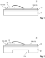
- Fig. 1 shows a cross-sectional side view on an example of a semiconductor module according to the second aspect comprising a first metal layer made e.g. of copper.
- Fig. 1 shows a semiconductor module 10 comprising a first metal layer 11, a ceramic layer 12 applied on the first metal layer 11, a second metal layer 13 applied at least in part on the ceramic layer 12, and a semiconductor die 14 attached on a portion of the second metal layer 13.
- the second metal layer 13 can comprises a first layer portion 13A and a second layer portion 13B and the semiconductor die 14 can applied on the first layer portion 13A.
- the semiconductor die 14 can be a semiconductor transistor die 14, in particular a power semiconductor transistor die 14.
- the term "power semiconductor transistor die” may refer to a semiconductor die providing at least one of high voltage blocking or high current-carrying capabilities.
- a power semiconductor die may be configured for high currents having a maximum current value of a few Amperes, such as e.g. 10 A, or a maximum current value of up to or even exceeding 100 A.
- voltages associated with such current values may have values of a few Volts to a few tens or hundreds or even thousands of Volts.
- the semiconductor die 14 can be one or more of a semiconductor transistor die, a power semiconductor transistor die, an IGBT, or a MOSFET. However, as already mentioned before, the semiconductor die 14 can also be another die like a diode die or a driver die.
- semiconductor die 14 as described herein may be manufactured from an elemental semiconductor material (e.g. Si) or from a wide band gap semiconductor material or a compound semiconductor material (e.g. SiC, GaN, SiGe, GaAs).
- an elemental semiconductor material e.g. Si
- a wide band gap semiconductor material e.g. SiC, GaN, SiGe, GaAs.
- the first metal layer 11 can, for example, be made of or comprise copper or a copper alloy and can have a thickness in a range from 50 ⁇ m to 600 ⁇ m depending on the thickness of the ceramic layer and the preferred thickness ratio between both layers.
- the ceramic layer 12 can be made of or comprise Si3N4, SiO or AlN, Zirconia doped alumina, ZrO, SiAlON or mixtures thereof or layerings thereof and can have a thickness in a range from 10 ⁇ m to 40 ⁇ m.
- the relative thicknesses of the first metal layer 11 and the ceramic layer 12 can also be adjusted so that a thickness ratio of the ceramic layer 12 to the first metal layer 11 is at least 1:5 or 1:15.
- a thick first metal layer 11 provides both the heatspreading as well as the compressive stress for the thin ceramic layer 12.
- a compressive stress can be generated in the ceramic layer 12 which can be in a range from 0,5 MPa to 20 MPa.
- the ceramic layer 12 is deposited on the first metal layer 11 by PECVD as was described before at process temperatures below 400°C.
- Both the thickness ratio between the ceramic layer 12 and the first metal layer 11 and the low process temperature of the PECVD deposition process lead to the compressive stress within the ceramic layer 12 with which bowing of the semiconductor module 10 can be prevented or at least be kept within acceptable limits.
- the second metal layer 13 can have a thickness in a range from 10 ⁇ m to 120 ⁇ m. In this respect it is important to note that the current carrying capacity for power connections results mostly from wide traces within an aspect ratio width to thickness of the traces of 10:1 or more.
- a heat sink can be attached to the backside of the first metallic layer 11 either by the manufacturer or by the customer and thermally coupled to the first metallic layer via a thermal interface layer.
- Fig. 2 shows a cross-sectional side view on an example of a semiconductor module according to the second aspect comprising a first metal layer made of aluminum and comprising a recess for inserting a water cooler.
- Fig. 2 shows a semiconductor module 20 comprising a first metal layer 21, a ceramic layer 22 applied on the first metal layer 21, a second metal layer 23 applied at least in part on the ceramic layer 22, and a semiconductor die 24 attached on a portion of the second metal layer 23.
- the ceramic layer 22 may correspond to the ceramic layer 12
- the second metallic layer 23 may correspond to the second metallic layer 13
- the semiconductor die 24 may correspond to the semiconductor die 14.
- the semiconductor module 20 of Fig. 2 has a first metallic layer 21, which has a recess 21A on its rear side.
- a water cooling system can be suitably integrated into this recess 21, which is connected to a cooling circuit, for example.
- the first metallic layer 21 is therefore preferably made of aluminum instead of copper, since aluminum is in general easier to machine than copper with regard to the shaping of the recess 21A.
- the semiconductor modules shown in Figs. 1 and 2 can be provided with a suitable encapsulant, which is usually a molding compound comprising a polymer such as an epoxy resin. This can be applied in such a way that the respective backsides of the first metallic layers 11 and 21 remain uncovered to enable heat dissipation by means of a heat sink or water cooling in the finished product.
- a suitable encapsulant which is usually a molding compound comprising a polymer such as an epoxy resin.
- Example 1 is a method for fabricating a semiconductor module, the method comprising providing a first metal layer, applying a ceramic layer by means of plasma enhanced chemical vapor deposition to the first metal layer, applying a second metal layer at least in part to the ceramic layer, and attaching a semiconductor die on a portion of the second metal layer.
- Example 2 is the method according to Example 1, wherein a material of the ceramic layer comprises one or more of Si3N4, SiO or AlN, Zirconia doped alumina, ZrO, SiAlON or mixtures thereof or layerings thereof.
- Example 3 is the method according to Example 1 or 2, further comprising applying the ceramic layer to a thickness in a range from 10 ⁇ m to 40 ⁇ m.
- Example 4 is the method according to any one of the preceding Examples, wherein a thickness ratio of the ceramic layer to the first metal layer is at least 1:5 or 1:15.
- Example 5 is the method according to any one of the preceding Examples, wherein the applied ceramic layer comprises a compressive stress in a range from 0,5 MPa to 20 MPa.
- Example 6 is the method according to any one of the preceding Examples, wherein the applied ceramic layer comprises a thermal resistance of less than 13 K/W based on a one mm 2 reference area.
- Example 7 is the method according to any one of the preceding Examples, further comprising applying the ceramic layer by using a process temperature of the plasma enhanced chemical vapor deposition of below 400°C or below 350°C or below 300°C or below 250°C.
- Example 8 is the method according to any one of the preceding Examples, further comprising applying the second metal layer to a thickness in a range from 10 ⁇ m to 120 ⁇ m.
- Example 9 is the method according to any one of the preceding Examples, further comprising applying the second metal layer by means of plasma enhanced chemical vapor deposition or by sputtering.
- Example 10 is the method according to any one of the preceding Examples, wherein the semiconductor die comprises one or more of a semiconductor transistor die, a power semiconductor transistor die, an IGBT, a MOSFET, a diode die, or a driver die.
- the semiconductor die comprises one or more of a semiconductor transistor die, a power semiconductor transistor die, an IGBT, a MOSFET, a diode die, or a driver die.
- Example 11 is a semiconductor module, comprising a first metal layer, a ceramic layer applied on the first metal layer, a second metal layer applied at least in part on the ceramic layer, and a semiconductor die attached on a portion of the second metal layer.
- Example 12 is the semiconductor module according to Example 11, wherein a material of the ceramic layer comprises one or more of Si3N4, SiO or AlN, Zirconia doped alumina, ZrO, SiAlON or mixtures thereof or layerings thereof.
- Example 13 is the semiconductor module according to Example 11 or 12, wherein the ceramic layer comprises a thickness in a range from 10 ⁇ m to 40 ⁇ m.
- Example 14 is the semiconductor module according to any one of Examples 11 to 13, wherein the first metal layer so that a thickness ratio of the ceramic layer to the first metal layer is at least 1:5 or 1:15.
- Example 15 is the semiconductor module according to any one of Examples 11 to 14, wherein the ceramic layer comprises a compressive stress in a range from 0,5 MPa to 20 MPa.
- Example 16 is the semiconductor module according to any one of Examples 11 to 15, wherein the ceramic layer comprises a thermal resistance less of than 13 K/W based on a one mm 2 reference area.
- Example 17 is the semiconductor module according to any one of Examples 11 to 16, wherein the second metal layer comprises a thickness in a range from 10 ⁇ m to 120 ⁇ m.
- Example 18 is the semiconductor module according to any one of Examples 11 to 17, wherein the semiconductor die comprises one or more of a semiconductor transistor die, a power semiconductor transistor die, an IGBT, a MOSFET, a diode die, or a driver die.
- the semiconductor die comprises one or more of a semiconductor transistor die, a power semiconductor transistor die, an IGBT, a MOSFET, a diode die, or a driver die.
Landscapes
- Engineering & Computer Science (AREA)
- Chemical & Material Sciences (AREA)
- Microelectronics & Electronic Packaging (AREA)
- Physics & Mathematics (AREA)
- General Physics & Mathematics (AREA)
- Condensed Matter Physics & Semiconductors (AREA)
- Power Engineering (AREA)
- Computer Hardware Design (AREA)
- Materials Engineering (AREA)
- Manufacturing & Machinery (AREA)
- Ceramic Engineering (AREA)
- Organic Chemistry (AREA)
- General Chemical & Material Sciences (AREA)
- Chemical Kinetics & Catalysis (AREA)
- Metallurgy (AREA)
- Mechanical Engineering (AREA)
- Inorganic Chemistry (AREA)
- Plasma & Fusion (AREA)
- Cooling Or The Like Of Semiconductors Or Solid State Devices (AREA)
Priority Applications (3)
| Application Number | Priority Date | Filing Date | Title |
|---|---|---|---|
| EP23161843.0A EP4431484A1 (de) | 2023-03-14 | 2023-03-14 | Verfahren zur herstellung eines halbleitermoduls mit einem substrat mit einer isolierenden keramischen schicht und halbleitermodul |
| CN202410284020.XA CN118658789A (zh) | 2023-03-14 | 2024-03-13 | 用于制造包括具有绝缘陶瓷层的衬底的半导体模块的方法以及半导体模块 |
| US18/604,588 US20240312795A1 (en) | 2023-03-14 | 2024-03-14 | Semiconductor module having a substrate with an insulating ceramic layer and a method for fabricating thereof |
Applications Claiming Priority (1)
| Application Number | Priority Date | Filing Date | Title |
|---|---|---|---|
| EP23161843.0A EP4431484A1 (de) | 2023-03-14 | 2023-03-14 | Verfahren zur herstellung eines halbleitermoduls mit einem substrat mit einer isolierenden keramischen schicht und halbleitermodul |
Publications (1)
| Publication Number | Publication Date |
|---|---|
| EP4431484A1 true EP4431484A1 (de) | 2024-09-18 |
Family
ID=85685645
Family Applications (1)
| Application Number | Title | Priority Date | Filing Date |
|---|---|---|---|
| EP23161843.0A Pending EP4431484A1 (de) | 2023-03-14 | 2023-03-14 | Verfahren zur herstellung eines halbleitermoduls mit einem substrat mit einer isolierenden keramischen schicht und halbleitermodul |
Country Status (3)
| Country | Link |
|---|---|
| US (1) | US20240312795A1 (de) |
| EP (1) | EP4431484A1 (de) |
| CN (1) | CN118658789A (de) |
Citations (2)
| Publication number | Priority date | Publication date | Assignee | Title |
|---|---|---|---|---|
| EP1909321A1 (de) * | 2005-06-06 | 2008-04-09 | DOWA Electronics Materials Co., Ltd. | Metall-keramik-verbundsubstrat und verfahren zu seiner herstellung |
| US20160014878A1 (en) * | 2014-04-25 | 2016-01-14 | Rogers Corporation | Thermal management circuit materials, method of manufacture thereof, and articles formed therefrom |
-
2023
- 2023-03-14 EP EP23161843.0A patent/EP4431484A1/de active Pending
-
2024
- 2024-03-13 CN CN202410284020.XA patent/CN118658789A/zh active Pending
- 2024-03-14 US US18/604,588 patent/US20240312795A1/en active Pending
Patent Citations (2)
| Publication number | Priority date | Publication date | Assignee | Title |
|---|---|---|---|---|
| EP1909321A1 (de) * | 2005-06-06 | 2008-04-09 | DOWA Electronics Materials Co., Ltd. | Metall-keramik-verbundsubstrat und verfahren zu seiner herstellung |
| US20160014878A1 (en) * | 2014-04-25 | 2016-01-14 | Rogers Corporation | Thermal management circuit materials, method of manufacture thereof, and articles formed therefrom |
Also Published As
| Publication number | Publication date |
|---|---|
| US20240312795A1 (en) | 2024-09-19 |
| CN118658789A (zh) | 2024-09-17 |
Similar Documents
| Publication | Publication Date | Title |
|---|---|---|
| EP0746022B1 (de) | Hybrid-Multichip-Modul und Verfahren zur seiner Herstellung | |
| US7727813B2 (en) | Method for making a device including placing a semiconductor chip on a substrate | |
| KR100957078B1 (ko) | 전기적으로 절연된 전력 장치 패키지 | |
| US20160126197A1 (en) | Semiconductor device having a stress-compensated chip electrode | |
| US20250149432A1 (en) | Packaged electronic devices having dielectric substrates with thermally conductive adhesive layers | |
| CN104392985A (zh) | 包括衬底的多芯片器件 | |
| US9093437B2 (en) | Packaged vertical power device comprising compressive stress and method of making a packaged vertical power device | |
| US20170171978A1 (en) | Power module and manufacturing method thereof | |
| EP4170708A1 (de) | Elektronisches modul mit einem halbleitergehäuse mit integriertem clip und befestigungselement | |
| US9117786B2 (en) | Chip module, an insulation material and a method for fabricating a chip module | |
| US11626351B2 (en) | Semiconductor package with barrier to contain thermal interface material | |
| US20240243031A1 (en) | Thermal Enhanced Power Semiconductor Package | |
| US20230378010A1 (en) | Power semiconductor devices having moisture barriers | |
| EP4431484A1 (de) | Verfahren zur herstellung eines halbleitermoduls mit einem substrat mit einer isolierenden keramischen schicht und halbleitermodul | |
| US11616040B2 (en) | Semiconductor dies having ultra-thin wafer backmetal systems, microelectronic devices containing the same, and associated fabrication methods | |
| US6727585B2 (en) | Power device with a plastic molded package and direct bonded substrate | |
| US20220278017A1 (en) | Power Electronics Carrier | |
| US11598904B2 (en) | Power semiconductor module and method for producing a power semiconductor module | |
| EP4307359A1 (de) | Leistungshalbleitermodulanordnung und verfahren zur herstellung davon | |
| US20210066174A1 (en) | Semiconductor device package assemblies and methods of manufacture | |
| US20230215776A1 (en) | Semiconductor device | |
| US20020149055A1 (en) | Semiconductor device including insulating substrate formed of single-crystal silicon chip | |
| US11887961B2 (en) | Semiconductor device, semiconductor arrangement and method for producing the same | |
| US20050184385A1 (en) | Semiconductor device with improved thermal characteristics |
Legal Events
| Date | Code | Title | Description |
|---|---|---|---|
| PUAI | Public reference made under article 153(3) epc to a published international application that has entered the european phase |
Free format text: ORIGINAL CODE: 0009012 |
|
| STAA | Information on the status of an ep patent application or granted ep patent |
Free format text: STATUS: THE APPLICATION HAS BEEN PUBLISHED |
|
| AK | Designated contracting states |
Kind code of ref document: A1 Designated state(s): AL AT BE BG CH CY CZ DE DK EE ES FI FR GB GR HR HU IE IS IT LI LT LU LV MC ME MK MT NL NO PL PT RO RS SE SI SK SM TR |
|
| STAA | Information on the status of an ep patent application or granted ep patent |
Free format text: STATUS: REQUEST FOR EXAMINATION WAS MADE |
|
| 17P | Request for examination filed |
Effective date: 20241220 |