EP4431236A1 - Composite polishing pad including carbon nanotubes, and method for producing same - Google Patents
Composite polishing pad including carbon nanotubes, and method for producing same Download PDFInfo
- Publication number
- EP4431236A1 EP4431236A1 EP21964181.8A EP21964181A EP4431236A1 EP 4431236 A1 EP4431236 A1 EP 4431236A1 EP 21964181 A EP21964181 A EP 21964181A EP 4431236 A1 EP4431236 A1 EP 4431236A1
- Authority
- EP
- European Patent Office
- Prior art keywords
- polishing pad
- carbon nanotubes
- cmp
- composite polishing
- substrate layer
- Prior art date
- Legal status (The legal status is an assumption and is not a legal conclusion. Google has not performed a legal analysis and makes no representation as to the accuracy of the status listed.)
- Pending
Links
Images
Classifications
-
- B—PERFORMING OPERATIONS; TRANSPORTING
- B24—GRINDING; POLISHING
- B24B—MACHINES, DEVICES, OR PROCESSES FOR GRINDING OR POLISHING; DRESSING OR CONDITIONING OF ABRADING SURFACES; FEEDING OF GRINDING, POLISHING, OR LAPPING AGENTS
- B24B37/00—Lapping machines or devices; Accessories
- B24B37/11—Lapping tools
- B24B37/20—Lapping pads for working plane surfaces
- B24B37/24—Lapping pads for working plane surfaces characterised by the composition or properties of the pad materials
-
- B—PERFORMING OPERATIONS; TRANSPORTING
- B24—GRINDING; POLISHING
- B24B—MACHINES, DEVICES, OR PROCESSES FOR GRINDING OR POLISHING; DRESSING OR CONDITIONING OF ABRADING SURFACES; FEEDING OF GRINDING, POLISHING, OR LAPPING AGENTS
- B24B37/00—Lapping machines or devices; Accessories
- B24B37/11—Lapping tools
- B24B37/20—Lapping pads for working plane surfaces
- B24B37/26—Lapping pads for working plane surfaces characterised by the shape of the lapping pad surface, e.g. grooved
-
- B—PERFORMING OPERATIONS; TRANSPORTING
- B29—WORKING OF PLASTICS; WORKING OF SUBSTANCES IN A PLASTIC STATE IN GENERAL
- B29C—SHAPING OR JOINING OF PLASTICS; SHAPING OF MATERIAL IN A PLASTIC STATE, NOT OTHERWISE PROVIDED FOR; AFTER-TREATMENT OF THE SHAPED PRODUCTS, e.g. REPAIRING
- B29C33/00—Moulds or cores; Details thereof or accessories therefor
- B29C33/42—Moulds or cores; Details thereof or accessories therefor characterised by the shape of the moulding surface, e.g. ribs or grooves
-
- B—PERFORMING OPERATIONS; TRANSPORTING
- B29—WORKING OF PLASTICS; WORKING OF SUBSTANCES IN A PLASTIC STATE IN GENERAL
- B29C—SHAPING OR JOINING OF PLASTICS; SHAPING OF MATERIAL IN A PLASTIC STATE, NOT OTHERWISE PROVIDED FOR; AFTER-TREATMENT OF THE SHAPED PRODUCTS, e.g. REPAIRING
- B29C33/00—Moulds or cores; Details thereof or accessories therefor
- B29C33/44—Moulds or cores; Details thereof or accessories therefor with means for, or specially constructed to facilitate, the removal of articles, e.g. of undercut articles
-
- B—PERFORMING OPERATIONS; TRANSPORTING
- B29—WORKING OF PLASTICS; WORKING OF SUBSTANCES IN A PLASTIC STATE IN GENERAL
- B29C—SHAPING OR JOINING OF PLASTICS; SHAPING OF MATERIAL IN A PLASTIC STATE, NOT OTHERWISE PROVIDED FOR; AFTER-TREATMENT OF THE SHAPED PRODUCTS, e.g. REPAIRING
- B29C41/00—Shaping by coating a mould, core or other substrate, i.e. by depositing material and stripping-off the shaped article; Apparatus therefor
- B29C41/003—Shaping by coating a mould, core or other substrate, i.e. by depositing material and stripping-off the shaped article; Apparatus therefor characterised by the choice of material
-
- B—PERFORMING OPERATIONS; TRANSPORTING
- B29—WORKING OF PLASTICS; WORKING OF SUBSTANCES IN A PLASTIC STATE IN GENERAL
- B29C—SHAPING OR JOINING OF PLASTICS; SHAPING OF MATERIAL IN A PLASTIC STATE, NOT OTHERWISE PROVIDED FOR; AFTER-TREATMENT OF THE SHAPED PRODUCTS, e.g. REPAIRING
- B29C41/00—Shaping by coating a mould, core or other substrate, i.e. by depositing material and stripping-off the shaped article; Apparatus therefor
- B29C41/02—Shaping by coating a mould, core or other substrate, i.e. by depositing material and stripping-off the shaped article; Apparatus therefor for making articles of definite length, i.e. discrete articles
-
- B—PERFORMING OPERATIONS; TRANSPORTING
- B29—WORKING OF PLASTICS; WORKING OF SUBSTANCES IN A PLASTIC STATE IN GENERAL
- B29C—SHAPING OR JOINING OF PLASTICS; SHAPING OF MATERIAL IN A PLASTIC STATE, NOT OTHERWISE PROVIDED FOR; AFTER-TREATMENT OF THE SHAPED PRODUCTS, e.g. REPAIRING
- B29C41/00—Shaping by coating a mould, core or other substrate, i.e. by depositing material and stripping-off the shaped article; Apparatus therefor
- B29C41/34—Component parts, details or accessories; Auxiliary operations
- B29C41/42—Removing articles from moulds, cores or other substrates
-
- B—PERFORMING OPERATIONS; TRANSPORTING
- B29—WORKING OF PLASTICS; WORKING OF SUBSTANCES IN A PLASTIC STATE IN GENERAL
- B29C—SHAPING OR JOINING OF PLASTICS; SHAPING OF MATERIAL IN A PLASTIC STATE, NOT OTHERWISE PROVIDED FOR; AFTER-TREATMENT OF THE SHAPED PRODUCTS, e.g. REPAIRING
- B29C41/00—Shaping by coating a mould, core or other substrate, i.e. by depositing material and stripping-off the shaped article; Apparatus therefor
- B29C41/34—Component parts, details or accessories; Auxiliary operations
- B29C41/50—Shaping under special conditions, e.g. vacuum
-
- B—PERFORMING OPERATIONS; TRANSPORTING
- B29—WORKING OF PLASTICS; WORKING OF SUBSTANCES IN A PLASTIC STATE IN GENERAL
- B29C—SHAPING OR JOINING OF PLASTICS; SHAPING OF MATERIAL IN A PLASTIC STATE, NOT OTHERWISE PROVIDED FOR; AFTER-TREATMENT OF THE SHAPED PRODUCTS, e.g. REPAIRING
- B29C59/00—Surface shaping of articles, e.g. embossing; Apparatus therefor
- B29C59/002—Component parts, details or accessories; Auxiliary operations
-
- B—PERFORMING OPERATIONS; TRANSPORTING
- B29—WORKING OF PLASTICS; WORKING OF SUBSTANCES IN A PLASTIC STATE IN GENERAL
- B29K—INDEXING SCHEME ASSOCIATED WITH SUBCLASSES B29B, B29C OR B29D, RELATING TO MOULDING MATERIALS OR TO MATERIALS FOR MOULDS, REINFORCEMENTS, FILLERS OR PREFORMED PARTS, e.g. INSERTS
- B29K2105/00—Condition, form or state of moulded material or of the material to be shaped
- B29K2105/06—Condition, form or state of moulded material or of the material to be shaped containing reinforcements, fillers or inserts
- B29K2105/16—Fillers
- B29K2105/165—Hollow fillers, e.g. microballoons or expanded particles
- B29K2105/167—Nanotubes
-
- B—PERFORMING OPERATIONS; TRANSPORTING
- B29—WORKING OF PLASTICS; WORKING OF SUBSTANCES IN A PLASTIC STATE IN GENERAL
- B29K—INDEXING SCHEME ASSOCIATED WITH SUBCLASSES B29B, B29C OR B29D, RELATING TO MOULDING MATERIALS OR TO MATERIALS FOR MOULDS, REINFORCEMENTS, FILLERS OR PREFORMED PARTS, e.g. INSERTS
- B29K2507/00—Use of elements other than metals as filler
- B29K2507/04—Carbon
-
- B—PERFORMING OPERATIONS; TRANSPORTING
- B29—WORKING OF PLASTICS; WORKING OF SUBSTANCES IN A PLASTIC STATE IN GENERAL
- B29K—INDEXING SCHEME ASSOCIATED WITH SUBCLASSES B29B, B29C OR B29D, RELATING TO MOULDING MATERIALS OR TO MATERIALS FOR MOULDS, REINFORCEMENTS, FILLERS OR PREFORMED PARTS, e.g. INSERTS
- B29K2995/00—Properties of moulding materials, reinforcements, fillers, preformed parts or moulds
- B29K2995/0037—Other properties
- B29K2995/007—Hardness
-
- B—PERFORMING OPERATIONS; TRANSPORTING
- B29—WORKING OF PLASTICS; WORKING OF SUBSTANCES IN A PLASTIC STATE IN GENERAL
- B29K—INDEXING SCHEME ASSOCIATED WITH SUBCLASSES B29B, B29C OR B29D, RELATING TO MOULDING MATERIALS OR TO MATERIALS FOR MOULDS, REINFORCEMENTS, FILLERS OR PREFORMED PARTS, e.g. INSERTS
- B29K2995/00—Properties of moulding materials, reinforcements, fillers, preformed parts or moulds
- B29K2995/0037—Other properties
- B29K2995/0094—Geometrical properties
-
- B—PERFORMING OPERATIONS; TRANSPORTING
- B29—WORKING OF PLASTICS; WORKING OF SUBSTANCES IN A PLASTIC STATE IN GENERAL
- B29L—INDEXING SCHEME ASSOCIATED WITH SUBCLASS B29C, RELATING TO PARTICULAR ARTICLES
- B29L2031/00—Other particular articles
- B29L2031/736—Grinding or polishing equipment
Definitions
- the present invention relates to a composite polishing pad including carbon nanotubes, and a method for producing the same.
- CMP Chemical mechanical polishing
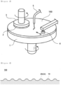
- FIG. 1 is a schematic diagram of a CMP apparatus.
- the CMP apparatus performs polishing by, while a carrier 3 firmly fixes a polishing object 2 (for example: wafer), pressurizing the polishing object onto a surface of a polishing pad 100 fixed on a rotary table 1.
- a liquid slurry (abrasive) is applied to the polishing pad 100 from a nozzle 5, and as a result, chemical and mechanical polishing is obtained.
- a conditioner 4 is pressurized against the polishing pad 100 at a position separated from the polishing object 1 during the polishing process, the surface of the polishing pad 100 is made to be roughened, and the rough surface state of the polishing pad is maintained.
- a polyurethane-based polishing pad In the CMP apparatus, a polyurethane-based polishing pad is generally used.
- existing polyurethane-based polishing pads have a disadvantage of short lifetime since abrasion progresses rapidly due to friction with high hardness nanoparticles, a polishing object and a diamond conditioner during a polishing process.
- existing polyurethane-based polishing pads have a disadvantage of not guaranteeing uniform polishing performance due to irregular surface roughness.
- the present invention has been devised to solve the conventional problems as described above, and is directed to providing a composite polishing pad for CMP having significantly improved polishing performance and lifetime, and a method for efficiently producing the same.
- the present invention provides a composite polishing pad for CMP, including:
- carbon nanotubes of the carbon nanotube layer may be embedded in the upper surface of the polymer substrate layer in an irregular net form structure.
- the irregular net form structure may be a structure formed by scattering the carbon nanotubes so that some thereof overlap each other.
- the polymer substrate layer may have shore hardness of 20D to 70D.
- the protrusion may have a maximum width of 10 um to 500 um, and a height of 3 um to 150 um.
- the carbon nanotubes may have a diameter of 1 nm to 50 nm, and a length of 1 um to 30 um.
- the protrusion may have a hemisphere-like shape.
- the present invention provides a method for producing a composite polishing pad for CMP, including the steps of:
- the step (b) above may be performed under vacuum.
- the present invention provides a method for producing a composite polishing pad for CMP, including the steps of:
- the embossing treatment in the step (d) may be conducted by pressurizing the upper surface of the substrate-removed carbon nanotubes with a mold having a plurality of protrusions engraved therein under a heating condition.
- the step (b) may be performed under vacuum.
- the composite polishing pad for CMP of the present invention includes a carbon nanotube layer with carbon nanotubes embedded in and fixed to the upper surface of a polymer substrate layer, thereby providing improved polishing performance and lifetime.
- a method for producing a composite polishing pad for CMP of the present invention provides a method capable of efficiently producing the polishing pad.
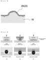
- a composite polishing pad for CMP of the present invention includes, as shown in FIG. 2 to FIG. 3 ,
- the composite polishing pad of the present invention has a characteristic of significantly improving polishing efficiency and lifetime by the above structure.
- the carbon nanotubes of the carbon nanotube layer 20 may be embedded in the surface of the polymer substrate layer 10 in an irregular net form structure, as shown in FIG. 2 and FIG. 3 .
- the irregular net form structure may be a structure formed by scattering the carbon nanotubes so that some thereof overlap.
- the meaning of scattering means disposing the carbon nanotubes through dispersion, and the meaning of overlap means that some of the carbon nanotubes overlap to strengthen a three-dimensional structure.
- the polymer substrate layer 10 may have shore hardness of 20D to 70D, preferably 30D to 45D.
- shore hardness of the polymer substrate layer satisfies the above-mentioned range, a contact area may be formed between the protrusion and a polishing object, and the lifetime and efficiency of a polishing pad may be improved as well, which is preferred.
- a polymer material with shore hardness of 20D to 70D forming the polymer substrate layer 10 one or more types selected from the group consisting of a polyurethane resin, a UV curable resin, a silicone resin and the like may be used.
- the material is not limited thereto, and materials known in the art may be used without limit as long as they do not adversely affect the present invention.
- a hard polymer material with shore hardness of 45D to 70D forming the hard polymer coating layer 30 one or more types selected from the group consisting of a polyurethane resin, a UV curable resin, a silicone resin and the like may be used.
- the material is not limited thereto, and materials known in the art may be used without limit as long as they do not adversely affect the present invention.
- the polymer substrate layer 10 may have a thickness of 2 mm to 50 mm, and more preferably 3 mm to 30 mm, except for the height of the protrusion.
- the polymer substrate layer 10 may be formed of, for example, two or more layers.
- the polymer substrate layer 10 may be a form in which a soft polymer substrate layer with shore hardness of 20D to 45D is disposed inside based on the polishing surface, and a hard polymer layer with shore hardness of 45D to 70D is stacked on the outer surface of the soft polymer material.
- the carbon nanotube layer may be provided on the surface of the hard polymer layer.
- the polymer substrate layer 10 is formed of a laminate of a soft polymer layer and a hard polymer layer, a wide contact area may be secured due to the soft polymer layer, and abrasive particles may be deeply pressed-in due to the hard polymer layer on the surface.
- FIG. 4 illustrates a contact pattern between a fine protrusion, an abrasive particle and a polishing object (for example: wafer) varying by differences in mechanical properties of the fine protrusion provided in the polishing pad.
- a fine protrusion having mechanically soft properties is readily deformed, thereby having a wide contact area, but is not able to press-in and polish a surface of a polishing object since a sufficient load is not applied to abrasive particles.
- it has a disadvantage in that it is readily worn, and thus continuous use as a polishing pad is impossible.
- a fine protrusion having mechanically strong properties has an advantage of, as shown in FIG. 4B , being able to deeply press-in and polish a surface of a polishing object by applying a load to abrasive particles, but has a disadvantage of not forming a wide contact area with the polishing object.
- the above-described effect may be obtained when forming a coating layer on a surface of a fine protrusion having mechanically soft properties using a material having mechanically strong properties (for example: material with high abrasion resistance).
- the polymer substrate layer 10 when the polymer substrate layer 10 if formed of a laminate of a soft polymer layer and a hard polymer layer, it may have a thickness of 1 mm to 20 mm, and more preferably 2 mm to 10 mm, except for the height of the protrusion.
- the hard polymer layer may have a thickness of 5 um to 90 um, and more preferably 10 um to 40 um, except for the height of the protrusion.
- the coating layer thickness being less than the above-mentioned thickness is not preferred since the polishing pad is readily worn, and the coating layer being too thick is not preferred since abrasive particle holding power is reduced by the carbon nanotubes and the polishing contact area is reduced at the same time.
- the above-mentioned range may be properly adjusted by adjusting the density and length of the carbon nanotube.
- the protrusion may have a maximum width of 10 um to 500 um, and a height of 3 um to 150 um.
- the above maximum width and the height are not limited to these ranges, and may be properly adjusted depending on the polishing object and the polishing condition.
- the protrusion may have, for example, a hemisphere-like shape, however, the shape is not particularly limited. As shown in FIG. 2 and FIG. 3 , the protrusion includes the polymer substrate layer 10 and the carbon nanotube layer 20, and protrudes in an upward direction of the composite polishing pad.
- the composite polishing pad may have a structure in which pores do not exist between a polymer substrate layer 10 and carbon nanotubes embedded in and fixed to the substrate layer 10.
- the polymer substrate layer 10 and the carbon nanotubes embedded in and fixed to the substrate layer 10 may be bound more firmly, which is preferred.
- Such a structure in which pores do not exist may be formed by forming bonds between the layers under vacuum as to be described below.
- the expression that pores do not exist may mean that pores do not substantially exist.
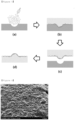
- the present invention also provides a method for producing a composite polishing pad for CMP, and the production method may include, as shown in FIG. 5 , the following steps (a) to (c):
- the method of scattering carbon nanotubes so that some thereof overlap each other in the step (a) may be performed using methods known in the art. For example, as shown in FIG. 5 , a method of spraying carbon nanotubes onto a mold through a nozzle may be used.
- the carbon nanotubes may be sprayed in a dispersed form in a solvent.
- the solvent may include water, ethanol, isopropyl alcohol and the like, but are not limited thereto.
- the coating of the step (b) may be performed using methods known in the art.
- methods such as spin coating and spray coating may be used, and the coating may be performed using other methods known in the art.
- the step (b) may be performed under vacuum. Coating under vacuum is preferred since it may prevent formation of pores between the carbon nanotubes and the polymer substrate layer, and the carbon nanotubes may be more strongly embedded and fixed accordingly.
- the present invention also provides another method for producing a composite polishing pad for CMP, and the production method may include the following steps (a) to (d) :
- the coating of the step (b) may be performed using methods known in the art.
- methods such as spin coating and spray coating may be used, and the coating may be performed using other methods known in the art.
- the separating of the substrate in the step (c) may be performed using methods such as mechanical silicon separation (release) and silicon etching.
- the embossing treatment in the step (d) may be conducted by pressurizing the upper surface of the substrate-removed carbon nanotubes with a mold having a plurality of protrusions engraved therein under a heating condition.
- the mold temperature may be from 200°C to 250°C, but is not limited thereto.
- the mold those made of metal materials such as nickel and copper may be used, and the micropattern may be manufactured using a micro electro-mechanical system (MEMS) process.
- MEMS micro electro-mechanical system
- the step (b) may be performed under vacuum. Coating under vacuum is preferred since it may prevent formation of pores between the carbon nanotubes and the polymer substrate layer, and the carbon nanotubes may be more strongly embedded and fixed accordingly.
- a carbon nanotube dispersion was prepared by dispersing carbon nanotubes into isopropyl alcohol. Then, the dispersion was coated on a mold in which a plurality of hemispherical protrusions having a radius of 50 um are engraved using a pneumatic nozzle. On the carbon nanotube-coated mold, a polyurethane resin (50 um) having shore hardness of 30D was coated under a vacuum atmosphere to form a polymer substrate layer having a thickness of 5 mm based on the upper end portion of the carbon nanotubes.
- the mold After curing the polymer substrate layer, the mold was separated and removed to produce the composite polishing pad of the present invention.
- a carbon nanotube dispersion was prepared by dispersing carbon nanotubes into isopropyl alcohol. Then, the dispersion was coated on a polypropylene substrate placed on a hot plate heated to 60°C using a pneumatic nozzle. On the carbon nanotube-coated mold, a polyurethane resin having shore hardness of 30D (trade name: Smooth-Cast TM 30D, manufactured by Smooth-On) was coated under a vacuum atmosphere to form a polymer substrate layer having a thickness of 5 mm based on the upper end portion of the carbon nanotubes.
- an embossing treatment was conducted by pressurization at 20O°C using a mold in which a plurality of hemispherical protrusions having a radius of 50 um are engraved, and as a result, a composite polishing pad of the present invention was produced.
- a carbon nanotube dispersion was prepared by dispersing carbon nanotubes into isopropyl alcohol. Then, the dispersion was coated on a polypropylene substrate placed on a hot plate heated to 60°C using a pneumatic nozzle. On the carbon nanotube-coated mold, a polyurethane resin having shore hardness of 45D (trade name: Smooth-Cast TM 45D, manufactured by Smooth-On) was coated through spin coating under a vacuum atmosphere to form a hard polymer layer having a thickness of 5 um based on the upper end portion of the carbon nanotubes.
- a polyurethane resin having shore hardness of 45D trade name: Smooth-Cast TM 45D, manufactured by Smooth-On
- the silicon substrate was mechanically separated to transfer the carbon nanotubes to the polyurethane.
- a polyurethane resin having shore hardness of 30D (trade name: Smooth-Cast TM 30D, manufactured by Smooth-On) was coated under a vacuum atmosphere to form a soft polymer layer having a thickness of 5 mm.
- an embossing treatment was conducted by pressurizing the carbon nanotubes from the upper portion at 200°C using a mold in which a plurality of hemispherical protrusions having a radius of 50 um are engraved, and as a result, a composite polishing pad of the present invention was produced.
- a polyurethane resin having shore hardness of 30D (trade name: Smooth-Cast TM 30D, manufactured by Smooth-On) was coated to form a polymer substrate layer having a thickness of 5 mm.
- an embossing treatment was conducted by pressurization at 20O°C using a mold in which a plurality of hemispherical protrusions having a radius of 50 um are engraved, and as a result, a composite polishing pad was produced.
Landscapes
- Engineering & Computer Science (AREA)
- Mechanical Engineering (AREA)
- Mechanical Treatment Of Semiconductor (AREA)
- Manufacture Of Macromolecular Shaped Articles (AREA)
- Polishing Bodies And Polishing Tools (AREA)
- Finish Polishing, Edge Sharpening, And Grinding By Specific Grinding Devices (AREA)
Abstract
Description
- The present invention relates to a composite polishing pad including carbon nanotubes, and a method for producing the same.
- Chemical mechanical polishing (CMP) is a key process for flattening and mirroring a wafer or a glass panel, and the polishing is performed by mechanical and chemical action of a polishing pad and a slurry containing nanoparticles.
-
FIG. 1 is a schematic diagram of a CMP apparatus. The CMP apparatus performs polishing by, while a carrier 3 firmly fixes a polishing object 2 (for example: wafer), pressurizing the polishing object onto a surface of apolishing pad 100 fixed on a rotary table 1. Specifically, while the carrier 3 and the rotary table 1 each independently rotate, a liquid slurry (abrasive) is applied to thepolishing pad 100 from anozzle 5, and as a result, chemical and mechanical polishing is obtained. In addition, as a conditioner 4 is pressurized against thepolishing pad 100 at a position separated from thepolishing object 1 during the polishing process, the surface of thepolishing pad 100 is made to be roughened, and the rough surface state of the polishing pad is maintained. - In the CMP apparatus, a polyurethane-based polishing pad is generally used. However, existing polyurethane-based polishing pads have a disadvantage of short lifetime since abrasion progresses rapidly due to friction with high hardness nanoparticles, a polishing object and a diamond conditioner during a polishing process. In addition, existing polyurethane-based polishing pads have a disadvantage of not guaranteeing uniform polishing performance due to irregular surface roughness.
-
Korean Laid-Open Patent Publication No. 10-2021-0002429 - The present invention has been devised to solve the conventional problems as described above, and is directed to providing a composite polishing pad for CMP having significantly improved polishing performance and lifetime, and a method for efficiently producing the same.
- In order to achieve the above object, the present invention provides a composite polishing pad for CMP, including:
- a polymer substrate layer including a plurality of protrusions formed on an upper surface thereof; and
- a carbon nanotube layer including carbon nanotubes embedded in and fixed to the upper portion of the substrate layer.
- In one embodiment of the present invention, carbon nanotubes of the carbon nanotube layer may be embedded in the upper surface of the polymer substrate layer in an irregular net form structure.
- In one embodiment of the present invention, the irregular net form structure may be a structure formed by scattering the carbon nanotubes so that some thereof overlap each other.
- In one embodiment of the present invention, the polymer substrate layer may have shore hardness of 20D to 70D.
- In one embodiment of the present invention, the protrusion may have a maximum width of 10 um to 500 um, and a height of 3 um to 150 um.
- In one embodiment of the present invention, the carbon nanotubes may have a diameter of 1 nm to 50 nm, and a length of 1 um to 30 um.
- In one embodiment of the present invention, the protrusion may have a hemisphere-like shape.
- In addition, the present invention provides a method for producing a composite polishing pad for CMP, including the steps of:
- (a) scattering carbon nanotubes on a mold having a plurality of protrusions engraved therein so that some thereof overlap each other;
- (b) forming a polymer substrate layer with a flat upper surface by coating a polymer on the upper portion of the carbon nanotubes; and
- (c) demolding the mold.
- In one embodiment of the present invention, the step (b) above may be performed under vacuum.
- In addition, the present invention provides a method for producing a composite polishing pad for CMP, including the steps of:
- (a) scattering carbon nanotubes on a substrate so that some thereof overlap each other;
- (b) forming a polymer substrate layer with a flat upper surface by coating a polymer on the upper portion of the carbon nanotubes;
- (c) separating and removing the substrate from the carbon nanotubes;
- (d) forming a plurality of protrusions including the polymer substrate layer and the carbon nanotube layer having an irregular net form structure by conducting an embossing treatment on the substrate-removed surface.
- In one embodiment of the present invention, the embossing treatment in the step (d) may be conducted by pressurizing the upper surface of the substrate-removed carbon nanotubes with a mold having a plurality of protrusions engraved therein under a heating condition.
- In one embodiment of the present invention, the step (b) may be performed under vacuum.
- The composite polishing pad for CMP of the present invention includes a carbon nanotube layer with carbon nanotubes embedded in and fixed to the upper surface of a polymer substrate layer, thereby providing improved polishing performance and lifetime.
- In addition, a method for producing a composite polishing pad for CMP of the present invention provides a method capable of efficiently producing the polishing pad.
-
-
FIG. 1 is a perspective view illustrating a structure of a typical CMP apparatus. -
FIG. 2 is a cross-sectional view schematically showing one embodiment of a composite polishing pad of the present invention. -
FIG. 3 is a cross-sectional view schematically showing a structure of a protrusion included in the composite polishing pad as one embodiment of the present invention. -
FIG. 4 is a diagram schematically illustrating a contact pattern between a fine protrusion, an abrasive particle and a polishing object depending on differences in mechanical properties of the fine protrusion provided in the polishing pad. -
FIG. 5 is a diagram schematically showing a method for producing a composite polishing pad as one embodiment of the present invention. -
FIG. 6 illustrates a SEM picture obtained by photographing a composite polishing pad in which carbon nanotubes are arranged in an irregular net form structure on the upper surface of the polymer substrate layer as one embodiment of the present invention. - Hereinafter, embodiments of the present invention will be described in detail with reference to accompanying drawings so that those skilled in the art may readily implement the present invention. However, the present invention may be embodied in various different forms, and is not limited to the embodiments described herein. The same reference numerals are used for like elements throughout the specification.
- When a certain constituent is referred to be "connected to, provided in, or installed on" another constituent, it needs to be understood that the certain constituent may be directed connected to or installed on the other constituent, but another constituent may also be present in between.
- A composite polishing pad for CMP of the present invention includes, as shown in
FIG. 2 to FIG. 3 , - a
polymer substrate layer 10 including a plurality of protrusions formed on an upper surface thereof; and - a
carbon nanotube layer 20 includingcarbon nanotubes 22 embedded in and fixed to the upper surface of the substrate layer. - The composite polishing pad of the present invention has a characteristic of significantly improving polishing efficiency and lifetime by the above structure.
- In other words, when abrasive particles are pressed into the carbon nanotube layer, a high force is applied to the abrasive particles due to high hardness of the surface of the carbon nanotubes and a polyurethane in which the carbon nanotubes are embedded to improve polishing efficiency. In addition, the lifetime of the polishing pad is also improved by improving mechanical strength due to the presence of the carbon nanotube surface layer.
- In one embodiment of the present invention, the carbon nanotubes of the
carbon nanotube layer 20 may be embedded in the surface of thepolymer substrate layer 10 in an irregular net form structure, as shown inFIG. 2 andFIG. 3 . - The irregular net form structure may be a structure formed by scattering the carbon nanotubes so that some thereof overlap. The meaning of scattering means disposing the carbon nanotubes through dispersion, and the meaning of overlap means that some of the carbon nanotubes overlap to strengthen a three-dimensional structure.
- In one embodiment of the present invention, the
polymer substrate layer 10 may have shore hardness of 20D to 70D, preferably 30D to 45D. When the hardness of the polymer substrate layer satisfies the above-mentioned range, a contact area may be formed between the protrusion and a polishing object, and the lifetime and efficiency of a polishing pad may be improved as well, which is preferred. - In one embodiment of the present invention, as a polymer material with shore hardness of 20D to 70D forming the
polymer substrate layer 10, one or more types selected from the group consisting of a polyurethane resin, a UV curable resin, a silicone resin and the like may be used. However, the material is not limited thereto, and materials known in the art may be used without limit as long as they do not adversely affect the present invention. - In addition, as a hard polymer material with shore hardness of 45D to 70D forming the hard polymer coating layer 30, one or more types selected from the group consisting of a polyurethane resin, a UV curable resin, a silicone resin and the like may be used. However, the material is not limited thereto, and materials known in the art may be used without limit as long as they do not adversely affect the present invention.
- In one embodiment of the present invention, the
polymer substrate layer 10 may have a thickness of 2 mm to 50 mm, and more preferably 3 mm to 30 mm, except for the height of the protrusion. - The
polymer substrate layer 10 may be formed of, for example, two or more layers. In other words, thepolymer substrate layer 10 may be a form in which a soft polymer substrate layer with shore hardness of 20D to 45D is disposed inside based on the polishing surface, and a hard polymer layer with shore hardness of 45D to 70D is stacked on the outer surface of the soft polymer material. In this case, the carbon nanotube layer may be provided on the surface of the hard polymer layer. - As described above, when the
polymer substrate layer 10 is formed of a laminate of a soft polymer layer and a hard polymer layer, a wide contact area may be secured due to the soft polymer layer, and abrasive particles may be deeply pressed-in due to the hard polymer layer on the surface. In addition, it is also possible to improve the polishing efficiency and lifetime of the polishing pad according to the function of each layer. - The above effect may be expressed as an image as in
FIG. 4. FIG. 4 illustrates a contact pattern between a fine protrusion, an abrasive particle and a polishing object (for example: wafer) varying by differences in mechanical properties of the fine protrusion provided in the polishing pad. - As shown in
FIG. 4A , a fine protrusion having mechanically soft properties is readily deformed, thereby having a wide contact area, but is not able to press-in and polish a surface of a polishing object since a sufficient load is not applied to abrasive particles. In addition, it has a disadvantage in that it is readily worn, and thus continuous use as a polishing pad is impossible. - On the other hand, a fine protrusion having mechanically strong properties (for example: fine protrusion made of a material with high abrasion resistance) has an advantage of, as shown in
FIG. 4B , being able to deeply press-in and polish a surface of a polishing object by applying a load to abrasive particles, but has a disadvantage of not forming a wide contact area with the polishing object. - However, as shown in
FIG. 4C , the above-described effect may be obtained when forming a coating layer on a surface of a fine protrusion having mechanically soft properties using a material having mechanically strong properties (for example: material with high abrasion resistance). - As described above, when the
polymer substrate layer 10 if formed of a laminate of a soft polymer layer and a hard polymer layer, it may have a thickness of 1 mm to 20 mm, and more preferably 2 mm to 10 mm, except for the height of the protrusion. In addition, the hard polymer layer may have a thickness of 5 um to 90 um, and more preferably 10 um to 40 um, except for the height of the protrusion. The coating layer thickness being less than the above-mentioned thickness is not preferred since the polishing pad is readily worn, and the coating layer being too thick is not preferred since abrasive particle holding power is reduced by the carbon nanotubes and the polishing contact area is reduced at the same time. However, the above-mentioned range may be properly adjusted by adjusting the density and length of the carbon nanotube. - In one embodiment of the present invention, the protrusion may have a maximum width of 10 um to 500 um, and a height of 3 um to 150 um. However, the above maximum width and the height are not limited to these ranges, and may be properly adjusted depending on the polishing object and the polishing condition.
- In one embodiment of the present invention, the protrusion may have, for example, a hemisphere-like shape, however, the shape is not particularly limited. As shown in
FIG. 2 andFIG. 3 , the protrusion includes thepolymer substrate layer 10 and thecarbon nanotube layer 20, and protrudes in an upward direction of the composite polishing pad. - In one embodiment of the present invention, the composite polishing pad may have a structure in which pores do not exist between a
polymer substrate layer 10 and carbon nanotubes embedded in and fixed to thesubstrate layer 10. When pores do not exist, thepolymer substrate layer 10 and the carbon nanotubes embedded in and fixed to thesubstrate layer 10 may be bound more firmly, which is preferred. - Such a structure in which pores do not exist may be formed by forming bonds between the layers under vacuum as to be described below. The expression that pores do not exist may mean that pores do not substantially exist.
- The present invention also provides a method for producing a composite polishing pad for CMP, and the production method may include, as shown in
FIG. 5 , the following steps (a) to (c): - (a) scattering carbon nanotubes on a mold having a plurality of protrusions engraved therein so that some thereof overlap each other;
- (b) forming a polymer substrate layer with a flat upper surface by coating a polymer on the upper portion of the carbon nanotubes; and
- (c) demolding the mold.
- The method of scattering carbon nanotubes so that some thereof overlap each other in the step (a) may be performed using methods known in the art. For example, as shown in
FIG. 5 , a method of spraying carbon nanotubes onto a mold through a nozzle may be used. Herein, the carbon nanotubes may be sprayed in a dispersed form in a solvent. Examples of the solvent may include water, ethanol, isopropyl alcohol and the like, but are not limited thereto. - The coating of the step (b) may be performed using methods known in the art. For example, methods such as spin coating and spray coating may be used, and the coating may be performed using other methods known in the art.
- In one embodiment of the present invention, the step (b) may be performed under vacuum. Coating under vacuum is preferred since it may prevent formation of pores between the carbon nanotubes and the polymer substrate layer, and the carbon nanotubes may be more strongly embedded and fixed accordingly.
- The present invention also provides another method for producing a composite polishing pad for CMP, and the production method may include the following steps (a) to (d) :
- (a) scattering carbon nanotubes on a substrate so that some thereof overlap each other;
- (b) forming a polymer substrate layer with a flat upper surface by coating a polymer on the upper portion of the carbon nanotubes;
- (c) separating and removing the substrate from the carbon nanotubes; and
- (d) forming a plurality of protrusions including the polymer substrate layer, the carbon nanotube layer arranged in a net form by conducting an embossing treatment on the substrate-removed surface.
- The coating of the step (b) may be performed using methods known in the art. For example, methods such as spin coating and spray coating may be used, and the coating may be performed using other methods known in the art.
- The separating of the substrate in the step (c) may be performed using methods such as mechanical silicon separation (release) and silicon etching.
- The embossing treatment in the step (d) may be conducted by pressurizing the upper surface of the substrate-removed carbon nanotubes with a mold having a plurality of protrusions engraved therein under a heating condition. In this case, the mold temperature may be from 200°C to 250°C, but is not limited thereto. As the mold, those made of metal materials such as nickel and copper may be used, and the micropattern may be manufactured using a micro electro-mechanical system (MEMS) process.
- In one embodiment of the present invention, the step (b) may be performed under vacuum. Coating under vacuum is preferred since it may prevent formation of pores between the carbon nanotubes and the polymer substrate layer, and the carbon nanotubes may be more strongly embedded and fixed accordingly.
- Hereinafter, the present invention will be described in detail with reference to examples in order to specifically describe the present invention. However, the examples according to the present invention may be modified to various different forms, and the scope of the present invention is not to be construed as being limited to the examples described below. Examples of the present invention are provided in order to more fully describe the present invention to those having average knowledge in the art.
- A carbon nanotube dispersion was prepared by dispersing carbon nanotubes into isopropyl alcohol. Then, the dispersion was coated on a mold in which a plurality of hemispherical protrusions having a radius of 50 um are engraved using a pneumatic nozzle. On the carbon nanotube-coated mold, a polyurethane resin (50 um) having shore hardness of 30D was coated under a vacuum atmosphere to form a polymer substrate layer having a thickness of 5 mm based on the upper end portion of the carbon nanotubes.
- After curing the polymer substrate layer, the mold was separated and removed to produce the composite polishing pad of the present invention.
- A carbon nanotube dispersion was prepared by dispersing carbon nanotubes into isopropyl alcohol. Then, the dispersion was coated on a polypropylene substrate placed on a hot plate heated to 60°C using a pneumatic nozzle. On the carbon nanotube-coated mold, a polyurethane resin having shore hardness of 30D (trade name: Smooth-Cast™ 30D, manufactured by Smooth-On) was coated under a vacuum atmosphere to form a polymer substrate layer having a thickness of 5 mm based on the upper end portion of the carbon nanotubes.
- After curing the polymer substrate layer, an embossing treatment was conducted by pressurization at 20O°C using a mold in which a plurality of hemispherical protrusions having a radius of 50 um are engraved, and as a result, a composite polishing pad of the present invention was produced.
- A carbon nanotube dispersion was prepared by dispersing carbon nanotubes into isopropyl alcohol. Then, the dispersion was coated on a polypropylene substrate placed on a hot plate heated to 60°C using a pneumatic nozzle. On the carbon nanotube-coated mold, a polyurethane resin having shore hardness of 45D (trade name: Smooth-Cast™ 45D, manufactured by Smooth-On) was coated through spin coating under a vacuum atmosphere to form a hard polymer layer having a thickness of 5 um based on the upper end portion of the carbon nanotubes.
- After curing the hard polymer layer, the silicon substrate was mechanically separated to transfer the carbon nanotubes to the polyurethane.
- On the hard polymer layer on the opposite side of the separated carbon nanotubes, a polyurethane resin having shore hardness of 30D (trade name: Smooth-Cast™ 30D, manufactured by Smooth-On) was coated under a vacuum atmosphere to form a soft polymer layer having a thickness of 5 mm.
- After curing the soft polymer substrate layer, an embossing treatment was conducted by pressurizing the carbon nanotubes from the upper portion at 200°C using a mold in which a plurality of hemispherical protrusions having a radius of 50 um are engraved, and as a result, a composite polishing pad of the present invention was produced.
- A polyurethane resin having shore hardness of 30D (trade name: Smooth-Cast™ 30D, manufactured by Smooth-On) was coated to form a polymer substrate layer having a thickness of 5 mm.
- After curing the polymer substrate layer, an embossing treatment was conducted by pressurization at 20O°C using a mold in which a plurality of hemispherical protrusions having a radius of 50 um are engraved, and as a result, a composite polishing pad was produced.
-
1: Rotary Table 2: Wafer 3: Carrier (Rotating Head) 4: Conditioner 5: Nozzle 10: Soft Polymer Substrate Layer 20: Carbon Nanotube Layer 22: Carbon Nanotube 30: Hard Polymer Coating Layer 100: Composite Polishing Pad
Claims (12)
- A composite polishing pad for CMP, comprising:a polymer substrate layer including a plurality of protrusions formed on an upper surface thereof; anda carbon nanotube layer including carbon nanotubes embedded in and fixed to the upper surface of the substrate layer.
- The composite polishing pad for CMP of claim 1, wherein the carbon nanotube layer comprises carbon nanotubes embedded in the polymer substrate layer in an irregular net form structure.
- The composite polishing pad for CMP of claim 2, wherein the irregular net form structure is a structure formed by scattering the carbon nanotubes so that some thereof overlap each other.
- The composite polishing pad for CMP of claim 1, wherein the polymer substrate layer has shore hardness of 20D to 70D.
- The composite polishing pad for CMP of claim 1, wherein the protrusion has a maximum width of 10 um to 500 um, and a height of 3 um to 150 um.
- The composite polishing pad for CMP of claim 1, wherein the carbon nanotubes have a diameter of 1 nm to 50 nm, and a length of 1 um to 30 um.
- The composite polishing pad for CMP of claim 1, wherein the protrusion has a hemisphere-like shape.
- A method for producing a composite polishing pad for CMP, comprising:(a) scattering carbon nanotubes on a mold having a plurality of protrusions engraved therein so that some thereof overlap each other;(b) forming a polymer substrate layer with a flat upper surface by coating a polymer on the upper portion of the carbon nanotubes; and(c) demolding the mold.
- The method for producing a composite polishing pad for CMP of claim 8, wherein (b) above is performed under vacuum.
- A method for producing a composite polishing pad for CMP, comprising:(a) scattering carbon nanotubes on a substrate so that some thereof overlap each other;(b) forming a polymer substrate layer with a flat upper surface by coating a polymer on the upper portion of the carbon nanotubes;(c) separating and removing the substrate from the carbon nanotubes; and(d) forming a plurality of protrusions including the polymer substrate layer and the carbon nanotube layer in an irregular net form structure by conducting an embossing treatment on the substrate-removed surface.
- The method for producing a composite polishing pad for CMP, of claim 10, wherein the embossing treatment in (e) above is conducted by pressurizing the upper surface of the substrate-removed carbon nanotubes with a mold having a plurality of protrusions engraved therein under a heating condition.
- The method for producing a composite polishing pad for CMP, of claim 10, wherein (b) above is performed under vacuum.
Applications Claiming Priority (1)
| Application Number | Priority Date | Filing Date | Title |
|---|---|---|---|
| PCT/KR2021/016562 WO2023085471A1 (en) | 2021-11-12 | 2021-11-12 | Composite polishing pad including carbon nanotubes, and method for producing same |
Publications (2)
| Publication Number | Publication Date |
|---|---|
| EP4431236A1 true EP4431236A1 (en) | 2024-09-18 |
| EP4431236A4 EP4431236A4 (en) | 2025-09-10 |
Family
ID=86336137
Family Applications (1)
| Application Number | Title | Priority Date | Filing Date |
|---|---|---|---|
| EP21964181.8A Pending EP4431236A4 (en) | 2021-11-12 | 2021-11-12 | Composite polishing pad with carbon nanotubes and method for producing the same |
Country Status (5)
| Country | Link |
|---|---|
| US (1) | US20240253178A1 (en) |
| EP (1) | EP4431236A4 (en) |
| JP (2) | JP2024522338A (en) |
| CN (1) | CN117545591A (en) |
| WO (1) | WO2023085471A1 (en) |
Family Cites Families (14)
| Publication number | Priority date | Publication date | Assignee | Title |
|---|---|---|---|---|
| US5441598A (en) * | 1993-12-16 | 1995-08-15 | Motorola, Inc. | Polishing pad for chemical-mechanical polishing of a semiconductor substrate |
| JP2001071269A (en) * | 1999-09-01 | 2001-03-21 | Mitsubishi Materials Corp | Electroplated whetstone |
| US6979248B2 (en) * | 2002-05-07 | 2005-12-27 | Applied Materials, Inc. | Conductive polishing article for electrochemical mechanical polishing |
| US20050227590A1 (en) * | 2004-04-09 | 2005-10-13 | Chien-Min Sung | Fixed abrasive tools and associated methods |
| TWI385050B (en) * | 2005-02-18 | 2013-02-11 | 奈平科技股份有限公司 | Special polishing pad for CMP, its manufacturing method and use thereof |
| JP2009072876A (en) * | 2007-09-21 | 2009-04-09 | Toyo Tire & Rubber Co Ltd | Polishing pad manufacturing method |
| WO2009120804A2 (en) * | 2008-03-28 | 2009-10-01 | Applied Materials, Inc. | Improved pad properties using nanoparticle additives |
| EP2552826A4 (en) * | 2010-03-30 | 2013-11-13 | Nantero Inc | Methods for arranging nanoscopic elements within networks, fabrics, and films |
| US8486319B2 (en) * | 2010-05-24 | 2013-07-16 | Integran Technologies Inc. | Articles with super-hydrophobic and/or self-cleaning surfaces and method of making same |
| KR101530365B1 (en) * | 2013-10-16 | 2015-06-18 | 새솔다이아몬드공업 주식회사 | Method of manufacturing the polishing pad conditioner |
| TWI769988B (en) * | 2015-10-07 | 2022-07-11 | 美商3M新設資產公司 | Polishing pads and systems and methods of making and using the same |
| JP7053015B2 (en) * | 2018-03-30 | 2022-04-12 | 山形県 | Method for manufacturing carbon nanotube composite resin molded product |
| KR102283399B1 (en) | 2018-12-26 | 2021-07-30 | 에스케이씨솔믹스 주식회사 | Composition for polishing pad, polishing pad and preparation method thereof |
| US20210323114A1 (en) * | 2020-04-21 | 2021-10-21 | Smart Pad LLC | Chemical-mechanical polishing pad with protruded structures |
-
2021
- 2021-11-12 EP EP21964181.8A patent/EP4431236A4/en active Pending
- 2021-11-12 WO PCT/KR2021/016562 patent/WO2023085471A1/en not_active Ceased
- 2021-11-12 CN CN202180099396.8A patent/CN117545591A/en active Pending
- 2021-11-12 US US18/289,607 patent/US20240253178A1/en active Pending
- 2021-11-12 JP JP2023571624A patent/JP2024522338A/en active Pending
-
2026
- 2026-01-07 JP JP2026001707A patent/JP2026042951A/en active Pending
Also Published As
| Publication number | Publication date |
|---|---|
| JP2024522338A (en) | 2024-06-18 |
| EP4431236A4 (en) | 2025-09-10 |
| CN117545591A (en) | 2024-02-09 |
| WO2023085471A1 (en) | 2023-05-19 |
| JP2026042951A (en) | 2026-03-11 |
| US20240253178A1 (en) | 2024-08-01 |
Similar Documents
| Publication | Publication Date | Title |
|---|---|---|
| CN110238752B (en) | Polishing product | |
| KR101507612B1 (en) | Improved chemical-mechanical polishing pads, and methods of making and using the same | |
| KR101442258B1 (en) | Improved chemical mechanical polishing pads, and methods of making and using them | |
| CN108136564B (en) | Polishing pad and system and method of making and using a polishing pad | |
| JP5671554B2 (en) | Organic fine particle loaded polishing pad, and method for producing and using the same | |
| US20010019940A1 (en) | Polishing pads and planarizing machines for mechanical or chemical-mechanical planarization of microelectronic-device substrate assemblies, and methods for making and using such pads and machines | |
| CN101925441A (en) | Plasma treated abrasive article and method of making same | |
| TWI432284B (en) | Methods and apparatus for forming a slurry polishing pad | |
| Logeeswaran et al. | Ultra-smooth metal surfaces generated by pressure-induced surface deformation of thin metal films | |
| US20090246504A1 (en) | Polishing Pad With Controlled Void Formation | |
| TW201032955A (en) | Polishing pads for chemical mechanical planarization and/or other polishing methods | |
| US20240253178A1 (en) | Composite polishing pad including carbon nanotubes, and method for producing same | |
| EP4431235A1 (en) | Composite polishing pad including highly abrasion-resistant thin film coating bound with carbon nanotubes, and method for producing same | |
| CN102246279A (en) | Carrier head membrane roughness to control polishing rate | |
| KR101453565B1 (en) | Chemical mechanical polishing method | |
| KR102531705B1 (en) | Composite polishing pad including carbon nanotubes and method for manufacturing the same | |
| KR102539172B1 (en) | Composite polishing pad comprising a thin film with high wear resistance stitched with carbon nanotubes and method for manufacturing the same | |
| TW581716B (en) | Material for use in carrier and polishing pads | |
| JP2004140130A (en) | Semiconductor substrate polishing pad and polishing method |
Legal Events
| Date | Code | Title | Description |
|---|---|---|---|
| STAA | Information on the status of an ep patent application or granted ep patent |
Free format text: STATUS: THE INTERNATIONAL PUBLICATION HAS BEEN MADE |
|
| PUAI | Public reference made under article 153(3) epc to a published international application that has entered the european phase |
Free format text: ORIGINAL CODE: 0009012 |
|
| STAA | Information on the status of an ep patent application or granted ep patent |
Free format text: STATUS: REQUEST FOR EXAMINATION WAS MADE |
|
| 17P | Request for examination filed |
Effective date: 20231113 |
|
| AK | Designated contracting states |
Kind code of ref document: A1 Designated state(s): AL AT BE BG CH CY CZ DE DK EE ES FI FR GB GR HR HU IE IS IT LI LT LU LV MC MK MT NL NO PL PT RO RS SE SI SK SM TR |
|
| DAV | Request for validation of the european patent (deleted) | ||
| DAX | Request for extension of the european patent (deleted) | ||
| A4 | Supplementary search report drawn up and despatched |
Effective date: 20250813 |
|
| RIC1 | Information provided on ipc code assigned before grant |
Ipc: B24B 37/24 20120101AFI20250807BHEP Ipc: B24B 37/26 20120101ALI20250807BHEP |