EP4430727B1 - Drahtlose stromübertragung - Google Patents
Drahtlose stromübertragung Download PDFInfo
- Publication number
- EP4430727B1 EP4430727B1 EP22812642.1A EP22812642A EP4430727B1 EP 4430727 B1 EP4430727 B1 EP 4430727B1 EP 22812642 A EP22812642 A EP 22812642A EP 4430727 B1 EP4430727 B1 EP 4430727B1
- Authority
- EP
- European Patent Office
- Prior art keywords
- chip sequence
- power
- chip
- preamble
- load
- Prior art date
- Legal status (The legal status is an assumption and is not a legal conclusion. Google has not performed a legal analysis and makes no representation as to the accuracy of the status listed.)
- Active
Links
Images


Classifications
-
- H—ELECTRICITY
- H02—GENERATION; CONVERSION OR DISTRIBUTION OF ELECTRIC POWER
- H02J—CIRCUIT ARRANGEMENTS OR SYSTEMS FOR SUPPLYING OR DISTRIBUTING ELECTRIC POWER; SYSTEMS FOR STORING ELECTRIC ENERGY
- H02J50/00—Circuit arrangements or systems for wireless supply or distribution of electric power
- H02J50/10—Circuit arrangements or systems for wireless supply or distribution of electric power using inductive coupling
- H02J50/12—Circuit arrangements or systems for wireless supply or distribution of electric power using inductive coupling of the resonant type
-
- H—ELECTRICITY
- H02—GENERATION; CONVERSION OR DISTRIBUTION OF ELECTRIC POWER
- H02J—CIRCUIT ARRANGEMENTS OR SYSTEMS FOR SUPPLYING OR DISTRIBUTING ELECTRIC POWER; SYSTEMS FOR STORING ELECTRIC ENERGY
- H02J50/00—Circuit arrangements or systems for wireless supply or distribution of electric power
- H02J50/80—Circuit arrangements or systems for wireless supply or distribution of electric power involving the exchange of data, concerning supply or distribution of electric power, between transmitting devices and receiving devices
Definitions
- the invention relates to wireless power transfer and in particular, but not exclusively, to wireless power transfer at higher power levels.
- wireless power transfer systems such as Qi based systems
- Qi supported only communication from the power receiver to the power transmitter using load modulation of the power transfer signal.
- developments of the standard have introduced bidirectional communication and many functions are supported by communication exchanges between the power receiver and the power transmitter.
- the communication from the power transmitter to the power receiver is accomplished by modulating the power transfer signal.
- the Invention seeks to preferably mitigate, alleviate or eliminate one or more of the above mentioned disadvantages singly or in any combination.
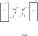
- a power transmitter for wirelessly providing power to a power receiver via an inductive power transfer signal; the power transmitter comprising: an output circuit comprising a transmitter coil arranged to generate the power transfer signal in response to a drive signal being applied to the output circuit; a driver arranged to generate the drive signal; a load detector for detecting load variations for the power transfer signal; a store for storing a first chip sequence and a second chip sequence, the second chip sequence having a length exceeding a length of the first chip sequence; a preamble presence detector arranged to correlate the second chip sequence with load variations of the power transfer signal to generate detection correlation values and to generate a preamble detection in response to a detection correlation value exceeding a preamble detection threshold; a load modulation receiver arranged to determine load modulation data symbols received from the power receiver following the preamble detection in response to a correlation of the first chip sequence and load variations of the power transfer signal; a synchronizer arranged to synchronize data symbol time intervals for the load modulation receiver in response
- the invention may provide improved performance in many embodiments and may in particular in many embodiments provide improved communication between a power receiver and a power transmitter. It may provide improved power transfer in many embodiments.
- the approach may allow improved communication, and in many embodiments may allow improved trade-off between different parameters and operating characteristics.
- the approach may e.g. allow highly reliable communication yet allow reduced modulation depth to be used.
- the approach may reduce electric noise and/or electromagnetic interference and provide improved electromagnetic compatibility.
- the approach may in many cases reduce or prevent acoustic noise.
- the approach may in many scenarios provide an improved trade-off between different parameters including computational resource requirements, data detection accuracy, bit error rate, data rate.
- the approach may switch between different chip sequences with different lengths for different purposes thereby providing differentiated optimization.
- the approach may provide improved data detection and synchronization which may lead to more reliable communication.
- the approach may provide advantageous backwards compatibility and e.g. may allow relatively easy modification of existing approaches, such as those used by the Qi Specifications.
- the approach may reuse much functionality from such existing approaches.
- the approach may allow for low complexity implementation yet provide highly efficient performance.
- the communication approach may be particularly advantageous for use in power transfer systems as bandwidth considerations may be less critical in such systems.
- a chip sequence may be a sequence/ pattern of modulation load values. Each of these modulation load values may be constant within a chip duration. Chip sequences for different data symbols have different sequences/ patterns of modulation load values.
- the length of the first chip sequence is not below 15 and not above 128 chips. In many embodiments, the length of the second chip sequence is not below 31 and not above 256 chips.
- the first chip sequence may be a chip sequence out of a plurality of data symbol chip sequences, each chip sequence being linked with a data symbol.
- the load modulation receiver may be arranged to determine load modulation data symbols received from the power receiver following the preamble detection in response to correlations of each of the plurality of data symbol chip sequences and load variations of the power transfer signal.
- a data symbol time interval is a time interval in which a data symbol is received.
- a data symbol time interval may have a duration equal to a duration of the first chip sequence.
- the alignment of the correlation of the first chip sequence and load variations of the power transfer signal to the data symbol time intervals may be such that the first chip sequence is correlated with load variations of the power transfer signal that are within one data symbol time interval.
- the alignment may be such that a first chip of the first chip sequence is aligned with a load variation sample occurring within a first symbol time interval and such that a second chip of the first chip sequence is aligned with a load variation sample (also) occurring within the first symbol time interval.
- the preamble presence detector may correlate the second chip sequence with a sequence of samples of load variations of the power transfer signal to generate detection correlation values.
- the correlation may be performed for different (time) alignments/ offsets between the second chip sequence and the load variations/ the sequence of samples of the load variations.
- the preamble presence detector may be arranged to determine that a detection of a preamble has occurred in response to a detection correlation value exceeding a preamble detection threshold.
- the load modulation receiver may be arranged to correlate the first chip sequence with load variations of the power transfer signal to generate symbol detection correlation values.
- the load modulation receiver may correlate the first chip sequence with a sequence of samples of load variations of the power transfer signal to generate detection correlation values. The correlation may be performed for different (time) alignments/ offsets between the first chip sequence and the load variations/ the sequence of samples of the load variations.
- the load modulation receiver may determine load modulation data symbols dependent on the symbol detection correlation values.
- a load modulation data symbol may be determined as a given data symbol if a symbol detection correlation value exceeds a threshold.
- the threshold may be dynamic and may e.g., be determined based on other correlations or symbol detection correlation values. For example, if multiple symbol detection correlation values are determined e.g. for different symbol chip sequences, a symbol value may be determined by a comparison of different symbol detection correlation values determined for the same data symbol time interval.
- the determination of data symbol values may in many embodiments be more complex than simply comparing a correlation result to a single fixed threshold (although this is of course possible). For example, comparisons may be made between correlations between different sequence values in cases where different data symbols may be encoded by different bit sequences. Further, a simple comparison to a single threshold may be inappropriate in cases where soft decision detection is performed. It is noted that such soft decision detection is a standard approach for communication, including Direct Sequence Spread Spectrum (DSSS) communication. For example, it is frequently used when error correcting coding is employed.
- DSSS Direct Sequence Spread Spectrum
- the load modulation receiver may be arranged to determine load modulation data symbols in response to a correlation of the first chip sequence and load variations of the power transfer signal following the preamble detection.
- the synchronization may be such that the first sequence is applied within a data symbol time interval.
- the load modulation receiver may be arranged to align the correlation of the first chip sequence with load variations of the power transfer signal to the data symbol time intervals by aligning the first chip sequence with load variations in data symbol time intervals of the power transfer signal.
- the load modulation receiver may be arranged to determine a first received data symbol value if the correlation value for the correlation of the first chip sequence and load variations of the power transfer signal in a first data symbol time interval exceeds a data symbol threshold.
- the synchronizer is arranged to determine the data symbol time intervals as repeating time intervals having a duration equal to a duration of the first chip sequence and having a predetermined time offset to the preamble detection.
- the predetermined time offset may specifically be a zero time offset.
- the predetermined time offset may specifically be a time offset of an integer number of chip time intervals/ durations.
- the length of the second chip sequence is no less than twice the length of the first chip sequence.
- a chip rate for the first chip sequence is higher than a chip rate for the second chip sequence.
- This may allow improved performance and/or facilitated implementation in many embodiments. In many embodiments it may allow reduced computational requirements.
- a chip rate for the first chip sequence is lower than a chip rate for the second chip sequence.
- This may allow improved performance and/or facilitated implementation in many embodiments. In many embodiments it may allow high data rate yet improved detection performance.
- the load modulation receiver is arranged to determine a first received data symbol value if the correlation value for the correlation of the first chip sequence and load variations of the power transfer signal in a first data symbol time interval exceeds a data symbol threshold, the data symbol threshold being lower than the preamble detection threshold.
- the modulation receiver is arranged to determine binary data symbol values corresponding to a sign of the correlation of the first chip sequence and load variations of the power transfer signal in the data symbol time intervals.
- a low complexity data detection can be used which in combination with the synchronization of the correlation may still provide reliable performance in many scenarios.
- the preamble presence detector is arranged to correlate load variations of the power transfer signal with a third chip sequence being a subset of the second chip sequence, and to initiate a correlation of the power transfer signal with the second chip sequence in response to a detection that a correlation value for the correlation between load variations of the power transfer signal with a third chip sequence exceeds a detection threshold.
- a length of the third chip sequence is no longer than a quarter of a length of the second chip sequence.
- the third chip sequence comprises at least some non-contiguous chips of the second chip sequence.
- the preamble presence detector may be arranged to only initiate a correlation of the power transfer signal with the second chip sequence if a correlation value for the correlation of the load variations of the power transfer signal with a third chip sequence exceeds a detection threshold.
- the third chip sequence is a subset of the second chip sequence having an autocorrelation higher than any autocorrelation of any chip sequence of contiguous chips of the second chip sequence with a length equal to a length of third chip sequence.
- This may provide improved operation and/or performance in many embodiments.
- the preamble presence detector is arranged to synchronize the second chip sequence to the drive signal when correlating the second chip sequence with load variations of the power transfer signal.
- This may provide improved operation and/or performance in many embodiments.
- the preamble presence detector is arranged to generate a noise estimate for the power transfer signal, and to adapt the preamble detection threshold in response to the noise estimate.
- This may provide improved operation and/or performance in many embodiments.
- a power receiver for wirelessly receiving power from a power transmitter via an inductive power transfer signal; the power receiver comprising: an input circuit comprising a receiver coil arranged to extract power from the power transfer signal; a store arranged to store a first chip sequence and a second chip sequence, the second chip sequence having a length exceeding a length of the first chip sequence; a preamble transmitter arranged to transmit a preamble by load modulating the power transfer signal by load variations corresponding to the second chip sequence; a data transmitter arranged to transmit data symbols to the power transmitter by load modulating the power transfer signal following transmission of the preamble, at least one data symbol being represented by a sequence of modulation load values corresponding to the first chip sequence; a synchronizer arranged to synchronize data symbol time intervals for the data transmitter with a timing of the transmission of the preamble, and wherein the data transmitter is arranged to align the sequence of modulation load values corresponding to the first chip sequence to the data symbol time intervals.
- a wireless power transfer system comprising a power transmitter and a power receiver as mentioned above.
- FIG. 7 illustrates an example of parts of two possible chip sequences.
- Each chip sequence comprises a sequence of chips with each chip having constant modulation load level selected from a set of modulation levels.
- the set of modulation levels is two, corresponding to a binary chip sequence where the modulation load levels may switch between two possible levels.
- a symbol time is thus divided into a plurality of chip intervals with the modulation load level for each chip interval being selected from a predetermined set of modulation load levels and with the modulation load level sequences of the chips being different for different chip sequences.
- each sequence includes at least ten chips, and often substantially more.
- each chip sequence may have a length of 2 N -1 where N is an integer of typically no less than 4.
- each of the stored chip sequences is assigned to a data symbol.
- each possible data symbol value that may need to be transmitted to the power transmitter may have a linked/ associated chip sequence.
- the set of chip sequences may comprise only two chip sequences.
- the chip sequences may as previously mentioned be the inverse of each other, and specifically one may arise from multiplication of the other by -1.
- each symbol (typically bit) time interval is divided into a plurality (of typically 31) chip intervals with the modulation load being constant within each chip interval and with the modulation loads varying (changing or not changing) between chip intervals in accordance with a pattern which is different for each data symbol.
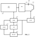
- the power transmitter comprises a load detector 209 which is arranged to detect load variations of the power transfer signal, and specifically it may determine a load variation sequence of the power transfer signal and/or drive signal.
- the load variation sequence may thus correspond to the received chip sequences when data is being transmitted.
- the load value of the drive signal e.g. the current and/or power
- the values may be normalized and quantized, e.g. if binary chip sequences are used, the load detector may generate a sequence of binary values e.g. representing a higher load and a lower load.
- a received chip sequence of load modulation is generated from the sampling of the signal(s) of the output circuit.
- the load detector 209 is coupled to the load modulation receiver 207 to which it provides the received chip sequence of modulation load values.
- the load modulation receiver 207 is further coupled to a receive chip sequence store 211.
- the receive chip sequence store 211 stores a set of reference chip sequences which specifically correspond to the chip sequences stored and used by the power receiver.
- the power transmitter 101 comprises a local representation of the chip sequences used by the power receiver.
- the receive chip sequence store 211 comprises a set of reference chip sequences with each reference chip sequence being linked to a specific data symbol.
- the power receiver and the power transmitter have stored corresponding links between reference chip sequences and data symbols.
- the receive chip sequence store 211 may store only a single data symbol chip sequence, namely that used to modulate the binary data symbols (and thus with the single stored data symbol chip sequence being equal to the chip sequence representing one binary data value and the inverse (typically sign inverted) chip sequence representing the other binary data value).
- the load modulation receiver 207 may then determine the data symbol as one linked with the chip sequence for which the associated correlation value is sufficiently high.
- the power receiver is capable of transmitting data to the power transmitter using load modulation with relatively long chip sequences for each data symbol.
- the approach may provide a substantially improved communication and operation in many embodiments.
- a substantially improved communication performance and reliability, and especially the symbol signal to noise ratio may be increased substantially.
- This may allow the modulation depth, and specifically the modulation load variations relative to the power transfer signal level/ power transfer level, to be reduced substantially.
- the modulation depth may be reduced by a factor of 10, 100, or even higher. This may reduce and mitigate many of the disadvantages of using load modulation and may e.g. reduce electromagnetic interference, reduce electrical noise, reduce mechanical noise, prevent or mitigate spurious oscillations etc.
- the improvement in signal to noise ratio may be increased by an amount corresponding to the sequence length.
- bit lengths of 63 or 127 may increase the symbol energy to noise ratio by a corresponding amount allowing the modulation depth to correspondingly be reduced by a factor of 63 or 127 while maintaining the same bit error rate.
- the system may be arranged to synchronize the load modulation communication to the power transfer signal/ drive signal.
- the data transmitter 509 may be arranged to generate the received chip sequence from samples of the loading of the power transfer signal (possible after matched filtering being applied).
- the synchronization may be of the sampling such that e.g. one sample is made per chip (possibly after matched filtering). Especially, if the chip rate is equal to N times the period of the power transfer signal, the sampling may also be synchronized to be once every N times. Thus, in many embodiments, the synchronization may be such that the sampling rate is equal to the chip frequency of the load modulation.
- the sampling may be a two stage process where a number of samples are generated at a higher frequency and then decimated to given sample rate. For example, for a chip duration of ten times the period of the power transfer signal, the sampler may take one sample every period. An averaging filter may then add the last ten samples, i.e. it may be a square window FIR filter that sums the ten most recent samples (with equal weights). The output of the sampling may then be the sampled output of this filter, such as specifically the output of every tenth period which coincides with the filter being a summation of the ten periods falling within a single chip. Thus, effectively the sampling at the synchronized time instants may be achieved by a suitably synchronized decimation at the output of the filter.
- only a single sampling of the analog signal of the output circuit is performed per chip.
- the timing of the sampling may for each sample be synchronized to occur in the center of the symbol duration.
- the operating frequency of the drive signal and the power transfer signal may thus be an integer multiple of the sampling rate of the sampling of the signal of the output circuit and /or an integer multiple of a chip frequency of the load modulation.
- the multiple may be the same and may specifically be one. Indeed, in many embodiments, the integer multiple is advantageously relatively low in order to allow efficient communication and a higher data rate. In many embodiments, the integer advantageously does not exceed 1, 3, 5, 10, or 20.
- Synchronization of the load modulation to the power transfer signal may in many practical implementations allow an increase of the chip rate and/or bit rate because it enables a reduction of the amount of sampling the power transmitter has to perform.
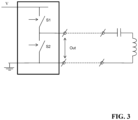
- the power receiver may change the load according to the chip sequence every cycle of the power transfer signal.
- the power receiver might change the load according to the chip sequence every N-th cycle of the power signal, reducing the chip frequency by a factor N.
- Synchronous modulation eases modulation detection at the power transmitter side by enabling this to apply a synchronous sampling technique and correlating the detected signal to the modulation sequence after that step.
- the approach may typically facilitate implementation substantially while achieving an efficient communication.
- the length of the chip sequences may be selected to the specific preferences and requirements of the individual embodiment and may be selected to provide a suitable compromise between communication reliability and performance (e.g. bit rate), data rate, bandwidth, modulation depth and associated disadvantages etc. In most embodiments, a length of no less than 8 and/or no more than 64 chips will provide suitable and advantageous performance for wireless power transfer systems, such as specifically for Qi systems.
- the set of chip sequences may include only two chip sequences.
- each symbol may be represented by one or the other chip sequence depending on the symbol value and thus each symbol may be a binary symbol (bit) and the communication may be a binary communication.
- the set of chip sequences may include more than two chip sequences and more than two different symbol values are possible.
- the set of chip sequences may comprise, say, three chip sequences allowing three different symbol values for each symbol being communicated by a chip sequence.
- a larger number of sequences may be included allowing each chip sequence/ data symbol to represent more data values thereby increasing the effective bit rate. Such an approach may in particular be suitable for longer chip sequences where larger differences in correlation values between chip sequences are feasible.
- the system may select two sequences out of these that have high autocorrelation and low cross-correlation.
- the sequences may be selected as a sequence with very high auto-correlation and the binary inverse chip sequence as this will have the lowest cross-correlation (normalized cross correlation of -1 using binary values of -1 and 1).
- the two sequences may then be used for binary communication allowing high reliability as the correlation performed by the load modulation receiver 207 will generate substantially different correlation values for the two possible chip sequences being received.
- chip sequences may be selected as maximum length sequences.
- chip sequences may be selected as maximum length sequences generated from polynomial the polynomial order chosen by the power receiver in accordance with a desired/ selected modulation depth and desired communication speed.
- pseudo noise sequences developed for, and used in, direct sequence spread spectrum communication and code division multiple access systems may tend to also be suitable for the described approach.
- the set of sequences may comprise mirror image or inverted chip sequences, i.e. for a given binary chip sequence, the set of chip sequences may also include the chip sequence for which all chips have the complementary value.
- the set of chip sequences may for each chip sequence also include the chip sequence resulting from a multiplication by -1 (equivalent to swapping between 0 and 1 for all chips for a chip sequence represented by the values of 1 and 0).
- the set of chip sequences may comprise only a chip sequence and the inverted chip sequence. It will be appreciated that in such embodiments, only a single representation needs to be stored to represent a pair of a chip sequence and the inverted chip sequence.
- inverted reference chip sequences can be considered equal to a multiplication of the binary data symbol and a single reference chip sequence (using the values of 1 and -1 to represent the binary values).
- the system may employ the following approach:
- An advantage of the described approach is that it provides improved backwards compatibility in many scenarios and require relatively little modifications to many power transfer systems. For example, a Qi power transfer system already uses load modulation and relatively little modification may be required to support the approach described hereinabove.
- functionality may be included that further improves backwards compatibility and which specifically may enable communication with legacy devices.
- the Inventors have realized that a critical factor of the load modulation operation in wireless power transfer system as described is the detection of data being present and the synchronization of the chip sequences to each other.
- the power transmitter may not know exactly when data is being transmitted or exactly when chip sequences start or stop.
- the chip synchronization to the power transfer signal/ drive signal may provide improved performance, e.g. allowing only a single load value sample to be taken per chip time, this may provide no information on when chip sequences are applied, i.e. when chip sequences start and stop.
- the data symbol timing may be uncertain.
- a receiver can continuously apply the chip sequences for every new chip period until a sufficiently high correlation is achieved and use this as an indication that a new data symbol has been detected, thereby providing data symbol timing via the symbol detection.
- a receiver can continuously apply the chip sequences for every new chip period until a sufficiently high correlation is achieved and use this as an indication that a new data symbol has been detected, thereby providing data symbol timing via the symbol detection.
- such an approach of trying to detect a data symbol for each new chip period increases the risk of false detections and may lead to errors in the data detection/ demodulation.
- the power receiver 105 specifically further comprises a preamble transmitter 515 which is arranged to transmit a preamble by load modulating the power transfer signal by load variations corresponding to the second chip sequence.
- the preamble transmitter 515 is specifically coupled to the chip sequence store 511 and the load modulator 513 and is arranged to retrieve a preamble chip sequence from the chip sequence store 511 and to control the load modulator 513 to load modulate the power transfer signal to apply the load variations to the power transfer signal in accordance with the preamble chip sequence.
- the preamble transmitter 515 may accordingly apply a load variation sequence in accordance with the preamble chip sequence. This load variation sequence is in the system used as a preamble to subsequent data transmission.
- preamble may refer to a synchronization sequence transmitted by the power receiver in connection with a transmission of data.
- preamble may include, and throughout may be replaced by, the term “synchronization sequence”.
- preamble chip sequence may include, and throughout may be replaced by, the term “synchronization chip sequence”.
- the power receiver furthermore comprises a power receiver synchronizer 517 which is arranged to synchronize the transmission of the preamble and the data symbol transmission, and specifically is arranged to control the preamble transmitter 515 to transmit the preamble prior to the subsequent transmission of one or more data symbols by the data transmitter 509.
- the power receiver synchronizer 517 may control the preamble transmitter 515 and the data transmitter 509 such that a data transmission of one or more data symbols/ bits (e.g. a data packet) is preceded by the transmission of a preamble.
- the power receiver synchronizer 517 may also synchronize the transmissions such that there is a fixed and typically predetermined time offset between the transmission of the preamble and the transmission of data symbols, i.e. between the modulation by the preamble chip sequence and by the data symbol chip sequences.
- a time offset may be zero such that the data symbol chips directly follow the preamble chip sequence.
- the periodic chip timing, and specifically the chip synchronization to the power transfer signal may be maintained across the transmission of the preamble chip sequence and the transmission of the data symbol chip sequences. Further, the last chip of the preamble chip sequence may be immediately followed by the first chip of the first data symbol chip sequence.
- Each data symbol chip sequence corresponds to a data symbol time interval, i.e. in each data symbol time interval, a data symbol chip sequence is transmitted/ loaded onto the power transfer signal.
- the synchronization of the data symbol chip sequences to the preamble chip sequence corresponds to an alignment and synchronization of the data symbol time intervals to the transmission of the preamble chip sequence. timing of the transmission of the preamble.
- the data transmitter 509 of FIG. 5 is accordingly arranged to apply the sequence of modulation load values corresponding to the data symbol chip sequence to the data symbol time intervals, and to align these data symbol time intervals to a timing of the transmission of the preamble.
- the length of the preamble chip sequence is longer than the length of the data symbol chip sequences, and typically is no less than twice as long.
- the length of the preamble chip sequence is thus substantially longer than the length of the data symbol chip sequences.
- the data symbol chip sequences may have a length of 31 chips whereas the preamble chip sequence has a length of 63 chips (or possibly 127 chips in some cases).
- the receive chip sequence store 211 of the power transmitter 101 stores not only the data symbol chip sequences but also the preamble chip sequence.
- the power transmitter 10 comprises a preamble presence detector 213 which is coupled to the receive chip sequence store 211 and the load detector 209.
- the preamble presence detector 213 retrieves the preamble chip sequence from the receive chip sequence store 211 and receives the load sequence from the load detector 209.
- the preamble presence detector 213 is arranged to correlate the preamble chip sequence and the load variations to determine a correlation value.
- the preamble presence detector 213 may proceed to perform such a correlation once every chip time interval. Specifically, during a time interval in which no data is being received, the preamble presence detector 213 may continuously determine preamble correlation values for each chip time interval where the preamble correlation value for a given timing is indicative of a correlation between the preamble chip sequence and the load variation sequence.
- the correlation value may be an absolute value of the preamble value.
- Correlation is a well-known approach for determining the similarity between two aligned sequences/ signals.
- correlation is between two sequences of values, of which one or both may be sample values of a signal.
- the correlation may be dependent on the alignment between the sequences as represented by the variable l in the above equation.
- correlations are determined as normalized correlations.
- a correlation value may thus in many cases be determined as a combination (often summation) of the results of element pair operations (typically multiplication) between corresponding elements of two sequences for a given time offset/ alignment of the two sequences.
- chip sequences are correlated with load variation sequences being samples of load variations of the power transfer signal.
- the correlation is performed for a given time offset/ alignment between the chip sequence and the load variations (specifically the load variation sample sequence) to determine a correlation value.
- the correlation may be performed repeatedly with different time offsets/ alignments. For example, for preamble detection the correlation may continuously be performed with an alignment that is increased by one sample time every time a new load sample is received.
- the load variation signal is for each new measurement/ sample continuously correlated with the preamble chip sequence to detect if a match is present.
- the power transfer signal is accordingly continuously monitored to detect if a preamble is considered present (as this is likely to result in a high correlation value for this time offset).
- the preamble presence detector 213 is arranged to evaluate the correlation values and specifically to compare them to a preamble detection threshold. If the correlation is performed when the load variation sequence corresponds to the transmitted preamble from the preamble transmitter 515, the load variations will match the preamble chip sequence and thus a relatively high correlation value will be generated. If the correlation is performed when the load variation sequence does not match the transmitted preamble, a low correlation with the preamble chip sequence will be present and a low correlation value will be generated.
- the preamble presence detector 213 is arranged to consider that a preamble has been detected if the correlation value exceeds the preamble detection threshold. Thus, the preamble presence detector 213 may during a time of no data symbols being received continuously monitor the load variations to detect if a preamble is being received.
- the power transmitter 101 further comprises a power transmitter synchronizer 215 which is coupled to the preamble presence detector 213 and the first communicator 207. If a preamble detection is generated by the preamble presence detector 213, the power transmitter synchronizer 215 is provided with an indication of the detection.
- the power transmitter synchronizer 215 is arranged to synchronize the data symbol time intervals for the load modulation receiver 207 in response to the timing of the preamble detection.
- the power transmitter synchronizer 215 may control the load modulation receiver 207 to apply the correlation with the data symbol chip sequences to be aligned with these data symbol time intervals. Each data symbol time interval may have a duration equal to a duration of a data symbol chip sequence.
- the correlation is aligned with the data symbol time intervals. Specifically, the correlation is performed with the data symbol chip sequences being within the data symbol time intervals. The correlation is specifically such that a start of the data symbol chip sequence aligns with a start of the data symbol time interval and/or such that an end of the data symbol chip sequence aligns with an end of the data symbol time interval.
- the detection of the preamble is thus used to synchronize the data symbol time intervals of the load modulation receiver 207 when performing the correlation such that this corresponds to the data symbol timing that was used by the power receiver.
- the data symbol correlation is not performed for all chip interval timings but is only performed once per data symbol time interval. This may substantially reduce the risk of a data symbol error resulting from noise. The probability of false detections of data being transmitted may be substantially reduced.
- the probability of detecting the preamble correctly is substantially increased in comparison to a correct detection of a data symbol.
- the probability of not only correctly detecting the start of a new data transmission but also of detecting and applying the correct data symbol timing when receiving data is very substantially increased.
- the correlation peak increases substantially for increased chip sequence length. Indeed, applying the described approach and increasing the chip sequence length from 31 to 63 bits tend to decrease the probability of detection errors, and even of the overall achievable bit error rate, by several orders of magnitude.
- chip sequences are accordingly used to provide highly efficient communication in a wireless power transfer system. Further, the system employs a preamble synchronization approach and further switches between one chip sequence length for the preamble and a shorter sequence length for the data symbols.
- the power transmitter and the power receiver are arranged to switch the correlation between different chip sequences with different length depending on whether a data symbols are being communicated or whether a preamble is transmitted or attempted to be detected.
- the power transmitter and the power receiver may be arranged to switch from a preamble chip sequence to a data symbol chip sequences when a preamble has been detected/ transmitted.
- the data symbols may be transmitted directly after the (synchronization) preamble, and specifically the last chip of the preamble sequence may directly be followed by the first bit of the first data value.
- subsequent data symbol time intervals may follow each other directly such that the last chip of one data symbol is directly followed by the first chip of the subsequent data symbol without any interval.
- known/ predetermined intervals may be present between different sequences.
- the power transmitter synchronizer 215 may be arranged to determine the data symbol time intervals as repeating time intervals that have a known/ predetermined duration, and typically with this duration being equal to the duration of the data symbol chip sequences. Furthermore, there may be a predetermined time offset from the time of the preamble detection, when the preamble chip sequence is aligned with the preamble, to the start of the first data symbol time interval. This predetermined time offset may often be zero.
- the load modulation receiver 207 may be arranged to determine the symbol values in response to a detection of whether the correlation value between the corresponding data symbol chip sequence is above a symbol detection threshold or not.
- the load modulation receiver 207 may simply be arranged to determine the symbol value to correspond to the sign of the correlation value for a single data symbol chip sequence. Indeed, in the case where the chip sequences for the two binary values are the inverse of each other, the correlation may directly indicate the symbol value. Further, the detection may for each data symbol time interval determine the data value to correspond to the sign of the correlation value without requiring any specific threshold to be applied. In other embodiments, it may be required that the absolute value of the correlation value exceeds a threshold, but this may be substantially lower than the threshold for detecting the preamble.
- the chip rates for the preamble chip sequence and for the data symbol chip sequences may be the same. This may typically allow facilitated implementation and may e.g. facilitate reuse of the same functionality for correlations to the different sequences.
- a generic correlator may be reconfigured simply by changing the chip sequence and changing the length of the correlation.
- the chip rates for the preamble chip sequence and for the data symbol chip sequences may be different.
- the chip rate for the preamble chip sequence may be lower than the chip rate for the data symbol chip sequences. This may be particularly advantageous in embodiments that are computationally resource limited. A correlation operation is typically resource demanding as it typically requires a multiplication and addition operation for each chip. Accordingly, as the chip length for the preamble correlation is substantially longer than for the data symbol chip sequences, the correlation may for a limited computational resource take longer to perform. In order to allow for such low computational resource implementations, the system may reduce the chip rate for the preamble transmission.
- the chip rate for the preamble chip sequence may be higher than for the data symbol chip sequences. Indeed, if the correlation resource is not a limitation, the chip rate for the preamble chip sequence may be increased such that the time and overhead required for transmitting the preamble may be reduced thereby reducing e.g. communication delays.
- the preamble presence detector 213 may be arranged to perform the preamble detection using a two stage approach. Specifically, rather than performing a full preamble chip sequence correlation for every chip time interval, a correlation may be performed with a shorter sequence formed by a subset of the preamble chip sequence and only if a correlation value of this correlation exceeds a threshold will a full correlation with the preamble chip sequence be performed.
- the preamble presence detector 213 may specifically be arranged to correlate the load variations of the power transfer signal with a subset chip sequence that is a subset of the preamble chip sequence.
- the subset chip sequence may be generated as a shorter chip sequence which is formed by a subset of the chips of the preamble chip sequence.
- an initial correlation is generated by performing an initial correlation which only includes some of the chips of the preamble chip sequence.
- the subset chip sequence may be substantially shorter than the preamble chip sequence and indeed may typically have the same length as the data symbol chip sequences.
- the length of the subset chip sequence is no longer than half, or a quarter of a length of the preamble chip sequence.
- the preamble chip sequence may have a length of 63 ort 127 chips and the subset chip sequence may have a length of 31 chips, equal to the length of the data symbol chip sequences.
- the subset chip sequence may be a sequence which is selected from the preamble chip sequence such that the selected chips form a subset chip sequence with a strong auto-correlation (and low cross-correlation to other possible load variations, such as specifically to the data symbol chip sequences).
- the subset chip sequence need not be generated as a contiguous sub-sequence of the preamble chip sequence. Rather, in many embodiments, the subset chip sequence may comprise at least some non-contiguous chips of the preamble chip sequence.
- the subset chip sequence may be selected to be formed by chip 1,2,3,10,11,20,.. etc of the preamble chip sequence.
- the initial correlation may then generate the initial correlation value by correlating chip 1 of the current load variation sequence with chip 1 of the preamble chip sequence, chip 2 of the current load variation sequence with chip 2 of the preamble chip sequence, chip 3 of the current load variation sequence with chip 3 of the preamble chip sequence, chip 10 of the current load variation sequence with chip 10 of the preamble chip sequence, etc.
- the initial correlation may then generate the initial correlation value by correlating chip 1 of the current load variation sequence with chip 1 of the preamble chip sequence, chip 2 of the current load variation sequence with chip 2 of the preamble chip sequence, chip 3 of the current load variation sequence with chip 3 of
- the subset chip sequence may as mentioned be selected to have a high auto-correlation.
- the subset chip sequence may be a subset of the preamble chip sequence that has an autocorrelation which is higher than the autocorrelation of any chip sequence of contiguous chips of the preamble chip sequence of the same length.
- Non-contiguous bits may be selected for the subset chip sequence such that this has a higher auto-correlation than if any series of consecutive bits in the preamble chip sequence were selected.
- Such a subset chip sequence may typically provide substantially improved performance with a more accurate initial detection. Further, this can be achieved without significant disadvantages as the correlation of non-contiguous bits is typically not any more difficult or problematic than a correlation with contiguous bits.
- the computational resource required for the initial correlation may be substantially lower than required for the full correlation. This may allow the initial correlation to be performed for e.g. each chip interval without requiring the computational resource necessary for a full preamble chip sequence correlation at every chip interval.
- the initial correlation value may be compared to a suitable initial threshold. If the threshold is not exceeded, it is considered highly likely that no preamble is currently received, and no further processing is performed for this chip interval. However, if the threshold is exceeded, it is considered likely, or at least reasonably possible, that a preamble is currently received. Accordingly, the preamble presence detector 213 may proceed to perform the full preamble chip sequence correlation and preamble detection for the current chip interval as previously described.
- the preamble presence detector 213 may be arranged to only initiate the full correlation of the load variations of the power transfer signal with the preamble chip sequence if indeed the initial correlation with the subset chip sequence results in a correlation value that exceeds the detection threshold. Otherwise, no further action is performed.
- the shorter length correlation and initial detection is generally less accurate than the full correlation.
- the threshold may however accordingly be set lower such that the likelihood of missing a preamble is sufficiently low. This will typically result in a number of false initial detections where no preamble is present. However, by subsequently performing the full preamble chip sequence correlation and detection, most such false detections can be detected and will not result in a preamble detection. Rather, the full preamble chip sequence correlation is required to be sufficiently high for there to be a match.
- the approach may typically provide the same detection accuracy as performing the full preamble chip sequence correlation for all chip sequences. However, it may typically be achieved with a substantially reduced average computational resource usage.
- the detection threshold may specifically in the individual embodiment be selected to provide the desired trade-off between computational resource usage and the risk of missing any preambles.
- the detection of the preamble is based on comparing the correlation value to a preamble detection threshold.
- a preamble detection threshold may be fixed and/or predetermined.
- the threshold may be dynamic and may be dependent on various operational properties.
- the preamble presence detector 213 may be arranged to generate a noise estimate for the power transfer signal. It will be appreciated that many different approaches are known for generating noise estimates and that any suitable approach may be used to determine such a noise estimate.
- the preamble presence detector 213 may be arranged to dynamically adapt the preamble detection threshold in response to the noise estimate. For example, for a high noise level, the detection threshold may be increased in order to reduce the risk of false detections. In other embodiments, the threshold may be decreased in order to reduce the risk of missing a preamble.
- a modulation load may be a load component of the loading of the power transfer signal/ drive signal caused by/ depending on/ varying with the load modulation.
- the preamble detection may be indicative of a preamble transmitted from the power receiver being received.
- preamble may be replaced by the term “synchronization sequence”.
- preamble chip sequence may be replaced by "synchronization chip sequence”.
- the invention can be implemented in any suitable form including hardware, software, firmware or any combination of these.
- the invention may optionally be implemented at least partly as computer software running on one or more data processors and/or digital signal processors.
- the elements and components of an embodiment of the invention may be physically, functionally and logically implemented in any suitable way. Indeed the functionality may be implemented in a single unit, in a plurality of units or as part of other functional units. As such, the invention may be implemented in a single unit or may be physically and functionally distributed between different units, circuits and processors.
Landscapes
- Engineering & Computer Science (AREA)
- Computer Networks & Wireless Communication (AREA)
- Power Engineering (AREA)
- Near-Field Transmission Systems (AREA)
Claims (15)
- Leistungssender (101) zum drahtlosen Bereitstellen von Leistung an einen Leistungsempfänger (105) über ein induktives Leistungsübertragungssignal; wobei der Leistungssender (101) Folgendes umfasst:eine Ausgabeschaltung (203, 103), die eine Senderspule (103) umfasst, die eingerichtet ist, um das Leistungsübertragungssignal als Antwort auf ein Ansteuersignal zu erzeugen, das an die Ausgabeschaltung (203, 103) angelegt wird;einen Treiber (201), der dazu eingerichtet ist, das Ansteuersignal zu erzeugen;einen Lastdetektor (209) zum Detektieren von Lastvariationen für das Leistungsübertragungssignal; dadurch gekennzeichnet, dass der Leistungssender (101) weiter Folgendes umfasst:einen Speicher (211) zum Speichern einer ersten Chipsequenz und einer zweiten Chipsequenz, wobei die zweite Chipsequenz eine Länge aufweist, die eine Länge der ersten Chipsequenz überschreitet;einen Präambelpräsenzdetektor (213), der eingerichtet ist, um die zweite Chipsequenz mit Lastvariationen des Leistungsübertragungssignals zu korrelieren, um Detektionskorrelationswerte zu erzeugen und eine Detektion einer Präambel als Antwort auf einen Detektionskorrelationswert zu bestimmen, der einen Präambeldetektionsschwellenwert überschreitet;einen Lastmodulationsempfänger (207), der eingerichtet ist, um Lastmodulationsdatensymbole nach der Detektion der Präambel in Abhängigkeit von einer Korrelation der ersten Chipsequenz und Lastvariationen des Leistungsübertragungssignals zu bestimmen;einen Synchronisierer (215), der eingerichtet ist, um Datensymbolzeitintervalle für den Lastmodulationsempfänger (207) als Antwort auf ein Timing der Detektion der Präambel zu synchronisieren, und wobei der Lastmodulationsempfänger (207) eingerichtet ist, um die Korrelation der ersten Chipsequenz und Lastvariationen des Leistungsübertragungssignals auf die Datensymbolzeitintervalle auszurichten.
- Einrichtung nach Anspruch 1, wobei der Synchronisierer (215) eingerichtet ist, um die Datensymbolzeitintervalle als sich wiederholende Zeitintervalle zu bestimmen, die eine Dauer gleich einer Dauer der ersten Chipsequenz aufweisen, und einen vorbestimmten Zeitversatz zur Detektion einer Präambel aufweisen.
- Einrichtung nach einem vorstehenden Anspruch, wobei die Länge der zweiten Chipsequenz nicht weniger als das Doppelte der Länge der ersten Chipsequenz ist.
- Einrichtung nach einem vorstehenden Anspruch, wobei eine Chiprate für die erste Chipsequenz höher ist als eine Chiprate für die zweite Chipsequenz.
- Einrichtung nach einem der vorstehenden Ansprüche 1 bis 3, wobei eine Chiprate für die erste Chipsequenz niedriger ist als eine Chiprate für die zweite Chipsequenz.
- Einrichtung nach einem vorstehenden Anspruch, wobei der Lastmodulationsempfänger (207) eingerichtet ist, um einen ersten empfangenen Datensymbolwert zu bestimmen, falls der Korrelationswert für die Korrelation der ersten Chipsequenz und Lastvariationen des Leistungsübertragungssignals in einem ersten Datensymbolzeitintervall einen Datensymbolschwellenwert überschreitet, wobei der Datensymbolschwellenwert niedriger ist als der Präambeldetektionsschwellenwert.
- Einrichtung nach einem vorstehenden Anspruch, wobei der Modulationsempfänger (207) eingerichtet ist, um binäre Datensymbolwerte zu bestimmen, die einem Vorzeichen der Korrelation der ersten Chipsequenz und Lastvariationen des Leistungsübertragungssignals in den Datensymbolzeitintervallen entsprechen.
- Einrichtung nach einem vorstehenden Anspruch, wobei der Präambelpräsenzdetektor (213) eingerichtet ist, um Lastvariationen des Leistungsübertragungssignals mit einer dritten Chipsequenz zu korrelieren, die eine Teilmenge der zweiten Chipsequenz ist, und um eine Korrelation des Leistungsübertragungssignals mit der zweiten Chipsequenz als Antwort auf eine Detektion zu initiieren, dass ein Korrelationswert für die Korrelation zwischen Lastvariationen des Leistungsübertragungssignals mit einer dritten Chipsequenz einen Detektionsschwellenwert überschreitet.
- Einrichtung nach Anspruch 8, wobei die dritte Chipsequenz eine Teilmenge der zweiten Chipsequenz ist, die eine höhere Autokorrelation aufweist als jede Autokorrelation einer beliebigen Chipsequenz von zusammenhängenden Chips der zweiten Chipsequenz mit einer Länge, die gleich der Länge der dritten Chipsequenz ist.
- Einrichtung nach einem vorstehenden Anspruch, wobei der Präambelpräsenzdetektor (213) eingerichtet ist, um die zweite Chipsequenz mit dem Ansteuersignal zu synchronisieren, wenn die zweite Chipsequenz mit Lastvariationen des Leistungsübertragungssignals korreliert wird.
- Einrichtung nach einem vorstehenden Anspruch, wobei der Präambelpräsenzdetektor (213) eingerichtet ist, um eine Rauschabschätzung für das Leistungsübertragungssignal zu erzeugen und den Präambeldetektionsschwellenwert als Antwort auf die Rauschabschätzung zu adaptieren.
- Leistungsempfänger (105) zum drahtlosen Empfangen von Leistung von einem Leistungssender (101) über ein induktives Leistungsübertragungssignal; wobei der Leistungsempfänger (105) Folgendes umfasst:eine Eingabeschaltung (107, 503), die eine Empfängerspule (107) umfasst, die eingerichtet ist, um Leistung aus dem Leistungsübertragungssignal zu extrahieren; dadurch gekennzeichnet, dass der Leistungsempfänger (105) weiter Folgendes umfasst:einen Speicher (511), der eingerichtet ist, um eine erste Chipsequenz und eine zweite Chipsequenz zu speichern, wobei die zweite Chipsequenz eine Länge aufweist, die eine Länge der ersten Chipsequenz übersteigt;einen Präambelsender (515), der eingerichtet ist, um eine Präambel durch Lastmodulieren des Leistungsübertragungssignals durch Lastvariationen entsprechend der zweiten Chipsequenz zu übertragen;einen Datensender (509), der eingerichtet ist, um Datensymbole an den Leistungssender (101) durch Lastmodulieren des Leistungsübertragungssignals nach der Übertragung der Präambel zu übertragen, wobei mindestens ein Datensymbol durch eine Sequenz von Modulationslastwerten repräsentiert wird, die der ersten Chipsequenz entsprechen;einen Synchronisierer (517), der eingerichtet ist, um Datensymbolzeitintervalle für den Datensender (509) mit einem Timing der Übertragung der Präambel zu synchronisieren, und wobei der Datensender (509) eingerichtet ist, um die Sequenz von Modulationslastwerten, die der ersten Chipsequenz entsprechen, auf die Datensymbolzeitintervalle auszurichten.
- Drahtloses Leistungsübertragungssystem, umfassend einen Leistungssender (101) nach einem der vorstehenden Ansprüche 1 bis 11 und einen Leistungsempfänger (105) nach Anspruch 12.
- Betriebsverfahren für einen Leistungssender (101), der einen Leistungsempfänger (105) drahtlos über ein induktives Leistungsübertragungssignal mit Leistung versorgt; der Leistungssender (101) umfasst:eine Ausgabeschaltung (203, 103), die eine Senderspule (103) umfasst, die eingerichtet ist, um das Leistungsübertragungssignal als Antwort auf ein Ansteuersignal zu erzeugen, das an die Ausgabeschaltung (203, 103) angelegt wird;
wobei das Verfahren Folgendes umfasstErzeugen des Ansteuersignals;Detektieren von Lastvariationen für das Leistungsübertragungssignal;dadurch gekennzeichnet, dass das Verfahren weiter Folgendes umfasst:Korrelieren einer zweiten Chipsequenz mit Lastvariationen des Leistungsübertragungssignals, um Detektionskorrelationswerte zu erzeugen, wobei die zweite Chipsequenz eine Länge aufweist, die eine Länge einer ersten Chipsequenz überschreitet;Bestimmen einer Detektion einer Präambel als Antwort auf einen Detektionskorrelationswert, der einen Präambeldetektionsschwellenwert überschreitet;Bestimmen von Lastmodulationsdatensymbolen nach der Detektion der Präambel in Abhängigkeit von einer Korrelation der ersten Chipsequenz und Lastvariationen des Leistungsübertragungssignals;Synchronisieren von Datensymbolzeitintervallen als Antwort auf ein Timing der Detektion der Präambel, undAusrichten der Korrelation der ersten Chipsequenz und Lastvariationen des Leistungsübertragungssignals auf die Datensymbolzeitintervalle. - Betriebsverfahren für einen Leistungsempfänger (105) der drahtlos Leistung von einem Leistungssender (101) über ein induktives Leistungsübertragungssignal empfängt; wobei der Leistungsempfänger (105) Folgendes umfasst:
eine Eingabeschaltung (107, 503), die eine Empfängerspule (107) umfasst, die eingerichtet ist, um Leistung aus dem Leistungsübertragungssignal zu extrahieren;
und dadurch gekennzeichnet, dass das Verfahren Folgendes umfasst:Übertragen einer Präambel durch Lastmodulieren des Leistungsübertragungssignals durch Lastvariationen entsprechend einer zweiten Chipsequenz, wobei die zweite Chipsequenz eine Länge aufweist, die eine Länge einer ersten Chipsequenz übersteigt;Übertragen von Datensymbolen an den Leistungssender (101) durch Lastmodulieren des Leistungsübertragungssignals nach Übertragung der Präambel, wobei mindestens ein Datensymbol durch eine Sequenz von Modulationslastwerten repräsentiert wird, die der ersten Chipsequenz entspricht;Synchronisieren von Datensymbolzeitintervallen für den Datensender (509) mit einem Timing der Übertragung der Präambel, undAusrichten der Sequenz von Modulationslastwerten, die der ersten Chipsequenz entsprechen, auf die Datensymbolzeitintervalle.
Priority Applications (1)
| Application Number | Priority Date | Filing Date | Title |
|---|---|---|---|
| EP25181139.4A EP4607756A3 (de) | 2021-11-10 | 2022-11-04 | Drahtlose stromübertragung |
Applications Claiming Priority (2)
| Application Number | Priority Date | Filing Date | Title |
|---|---|---|---|
| EP21207416 | 2021-11-10 | ||
| PCT/EP2022/080786 WO2023083707A1 (en) | 2021-11-10 | 2022-11-04 | Wireless power transfer |
Related Child Applications (1)
| Application Number | Title | Priority Date | Filing Date |
|---|---|---|---|
| EP25181139.4A Division EP4607756A3 (de) | 2021-11-10 | 2022-11-04 | Drahtlose stromübertragung |
Publications (3)
| Publication Number | Publication Date |
|---|---|
| EP4430727A1 EP4430727A1 (de) | 2024-09-18 |
| EP4430727B1 true EP4430727B1 (de) | 2025-07-02 |
| EP4430727C0 EP4430727C0 (de) | 2025-07-02 |
Family
ID=78621689
Family Applications (2)
| Application Number | Title | Priority Date | Filing Date |
|---|---|---|---|
| EP22812642.1A Active EP4430727B1 (de) | 2021-11-10 | 2022-11-04 | Drahtlose stromübertragung |
| EP25181139.4A Pending EP4607756A3 (de) | 2021-11-10 | 2022-11-04 | Drahtlose stromübertragung |
Family Applications After (1)
| Application Number | Title | Priority Date | Filing Date |
|---|---|---|---|
| EP25181139.4A Pending EP4607756A3 (de) | 2021-11-10 | 2022-11-04 | Drahtlose stromübertragung |
Country Status (10)
| Country | Link |
|---|---|
| US (1) | US12537394B2 (de) |
| EP (2) | EP4430727B1 (de) |
| JP (1) | JP2024543820A (de) |
| KR (1) | KR20240105425A (de) |
| CN (1) | CN118216058A (de) |
| ES (1) | ES3042064T3 (de) |
| MX (1) | MX2024005554A (de) |
| PL (1) | PL4430727T3 (de) |
| TW (1) | TW202337110A (de) |
| WO (1) | WO2023083707A1 (de) |
Families Citing this family (1)
| Publication number | Priority date | Publication date | Assignee | Title |
|---|---|---|---|---|
| EP4207554A1 (de) * | 2022-01-04 | 2023-07-05 | Koninklijke Philips N.V. | Drahtlose stromübertragung |
Family Cites Families (4)
| Publication number | Priority date | Publication date | Assignee | Title |
|---|---|---|---|---|
| JP2008028852A (ja) * | 2006-07-24 | 2008-02-07 | Felica Networks Inc | 情報処理端末、データ選択処理方法、およびプログラム |
| JP5670798B2 (ja) * | 2011-03-30 | 2015-02-18 | フェリカネットワークス株式会社 | 通信端末、通信方法、及びプログラム |
| KR20140124604A (ko) * | 2013-04-17 | 2014-10-27 | 삼성전자주식회사 | 무선 데이터 수신 방법 및 무선 데이터 수신 장치 |
| RU2706348C1 (ru) * | 2016-03-08 | 2019-11-18 | Конинклейке Филипс Н.В. | Беспроводной индуктивный перенос питания |
-
2022
- 2022-11-04 PL PL22812642.1T patent/PL4430727T3/pl unknown
- 2022-11-04 WO PCT/EP2022/080786 patent/WO2023083707A1/en not_active Ceased
- 2022-11-04 EP EP22812642.1A patent/EP4430727B1/de active Active
- 2022-11-04 ES ES22812642T patent/ES3042064T3/es active Active
- 2022-11-04 MX MX2024005554A patent/MX2024005554A/es unknown
- 2022-11-04 JP JP2024526465A patent/JP2024543820A/ja active Pending
- 2022-11-04 US US18/704,108 patent/US12537394B2/en active Active
- 2022-11-04 CN CN202280075174.7A patent/CN118216058A/zh active Pending
- 2022-11-04 KR KR1020247019025A patent/KR20240105425A/ko active Pending
- 2022-11-04 EP EP25181139.4A patent/EP4607756A3/de active Pending
- 2022-11-10 TW TW111142923A patent/TW202337110A/zh unknown
Also Published As
| Publication number | Publication date |
|---|---|
| TW202337110A (zh) | 2023-09-16 |
| PL4430727T3 (pl) | 2025-11-03 |
| MX2024005554A (es) | 2024-05-22 |
| JP2024543820A (ja) | 2024-11-26 |
| EP4607756A3 (de) | 2025-09-03 |
| WO2023083707A1 (en) | 2023-05-19 |
| ES3042064T3 (en) | 2025-11-18 |
| EP4430727A1 (de) | 2024-09-18 |
| US20250233456A1 (en) | 2025-07-17 |
| KR20240105425A (ko) | 2024-07-05 |
| EP4607756A2 (de) | 2025-08-27 |
| US12537394B2 (en) | 2026-01-27 |
| CN118216058A (zh) | 2024-06-18 |
| EP4430727C0 (de) | 2025-07-02 |
Similar Documents
| Publication | Publication Date | Title |
|---|---|---|
| US12506364B2 (en) | Wireless power transfer | |
| EP4270731A1 (de) | Drahtlose stromübertragung | |
| US12444998B2 (en) | Wireless power transfer | |
| US20250202290A1 (en) | Communication in a wireless power transfer system | |
| EP4430727B1 (de) | Drahtlose stromübertragung | |
| EP4593252A1 (de) | Drahtlose stromübertragung | |
| WO2023222419A1 (en) | Wireless power transfer |
Legal Events
| Date | Code | Title | Description |
|---|---|---|---|
| STAA | Information on the status of an ep patent application or granted ep patent |
Free format text: STATUS: UNKNOWN |
|
| STAA | Information on the status of an ep patent application or granted ep patent |
Free format text: STATUS: THE INTERNATIONAL PUBLICATION HAS BEEN MADE |
|
| PUAI | Public reference made under article 153(3) epc to a published international application that has entered the european phase |
Free format text: ORIGINAL CODE: 0009012 |
|
| STAA | Information on the status of an ep patent application or granted ep patent |
Free format text: STATUS: REQUEST FOR EXAMINATION WAS MADE |
|
| 17P | Request for examination filed |
Effective date: 20240610 |
|
| AK | Designated contracting states |
Kind code of ref document: A1 Designated state(s): AL AT BE BG CH CY CZ DE DK EE ES FI FR GB GR HR HU IE IS IT LI LT LU LV MC ME MK MT NL NO PL PT RO RS SE SI SK SM TR |
|
| GRAP | Despatch of communication of intention to grant a patent |
Free format text: ORIGINAL CODE: EPIDOSNIGR1 |
|
| STAA | Information on the status of an ep patent application or granted ep patent |
Free format text: STATUS: GRANT OF PATENT IS INTENDED |
|
| DAV | Request for validation of the european patent (deleted) | ||
| DAX | Request for extension of the european patent (deleted) | ||
| INTG | Intention to grant announced |
Effective date: 20250122 |
|
| RIN1 | Information on inventor provided before grant (corrected) |
Inventor name: STARING, ANTONIUS ADRIAAN MARIA Inventor name: AGAFONOV, ALEKSEI |
|
| GRAS | Grant fee paid |
Free format text: ORIGINAL CODE: EPIDOSNIGR3 |
|
| GRAA | (expected) grant |
Free format text: ORIGINAL CODE: 0009210 |
|
| STAA | Information on the status of an ep patent application or granted ep patent |
Free format text: STATUS: THE PATENT HAS BEEN GRANTED |
|
| AK | Designated contracting states |
Kind code of ref document: B1 Designated state(s): AL AT BE BG CH CY CZ DE DK EE ES FI FR GB GR HR HU IE IS IT LI LT LU LV MC ME MK MT NL NO PL PT RO RS SE SI SK SM TR |
|
| REG | Reference to a national code |
Ref country code: GB Ref legal event code: FG4D |
|
| REG | Reference to a national code |
Ref country code: CH Ref legal event code: EP |
|
| REG | Reference to a national code |
Ref country code: DE Ref legal event code: R096 Ref document number: 602022017060 Country of ref document: DE |
|
| REG | Reference to a national code |
Ref country code: IE Ref legal event code: FG4D |
|
| U01 | Request for unitary effect filed |
Effective date: 20250702 |
|
| U07 | Unitary effect registered |
Designated state(s): AT BE BG DE DK EE FI FR IT LT LU LV MT NL PT RO SE SI Effective date: 20250710 |
|
| REG | Reference to a national code |
Ref country code: ES Ref legal event code: FG2A Ref document number: 3042064 Country of ref document: ES Kind code of ref document: T3 Effective date: 20251118 |
|
| REG | Reference to a national code |
Ref country code: CH Ref legal event code: U11 Free format text: ST27 STATUS EVENT CODE: U-0-0-U10-U11 (AS PROVIDED BY THE NATIONAL OFFICE) Effective date: 20251201 |
|
| U20 | Renewal fee for the european patent with unitary effect paid |
Year of fee payment: 4 Effective date: 20251201 |
|
| PG25 | Lapsed in a contracting state [announced via postgrant information from national office to epo] |
Ref country code: IS Free format text: LAPSE BECAUSE OF FAILURE TO SUBMIT A TRANSLATION OF THE DESCRIPTION OR TO PAY THE FEE WITHIN THE PRESCRIBED TIME-LIMIT Effective date: 20251102 |
|
| PG25 | Lapsed in a contracting state [announced via postgrant information from national office to epo] |
Ref country code: NO Free format text: LAPSE BECAUSE OF FAILURE TO SUBMIT A TRANSLATION OF THE DESCRIPTION OR TO PAY THE FEE WITHIN THE PRESCRIBED TIME-LIMIT Effective date: 20251002 |
|
| PG25 | Lapsed in a contracting state [announced via postgrant information from national office to epo] |
Ref country code: HR Free format text: LAPSE BECAUSE OF FAILURE TO SUBMIT A TRANSLATION OF THE DESCRIPTION OR TO PAY THE FEE WITHIN THE PRESCRIBED TIME-LIMIT Effective date: 20250702 |
|
| PG25 | Lapsed in a contracting state [announced via postgrant information from national office to epo] |
Ref country code: GR Free format text: LAPSE BECAUSE OF FAILURE TO SUBMIT A TRANSLATION OF THE DESCRIPTION OR TO PAY THE FEE WITHIN THE PRESCRIBED TIME-LIMIT Effective date: 20251003 |
|
| PGFP | Annual fee paid to national office [announced via postgrant information from national office to epo] |
Ref country code: TR Payment date: 20251022 Year of fee payment: 4 |
|
| PGFP | Annual fee paid to national office [announced via postgrant information from national office to epo] |
Ref country code: CH Payment date: 20251201 Year of fee payment: 4 |
|
| PG25 | Lapsed in a contracting state [announced via postgrant information from national office to epo] |
Ref country code: CZ Free format text: LAPSE BECAUSE OF FAILURE TO SUBMIT A TRANSLATION OF THE DESCRIPTION OR TO PAY THE FEE WITHIN THE PRESCRIBED TIME-LIMIT Effective date: 20250702 |
|
| PGFP | Annual fee paid to national office [announced via postgrant information from national office to epo] |
Ref country code: PL Payment date: 20251023 Year of fee payment: 4 |
|
| PG25 | Lapsed in a contracting state [announced via postgrant information from national office to epo] |
Ref country code: RS Free format text: LAPSE BECAUSE OF FAILURE TO SUBMIT A TRANSLATION OF THE DESCRIPTION OR TO PAY THE FEE WITHIN THE PRESCRIBED TIME-LIMIT Effective date: 20251002 |
|
| PGFP | Annual fee paid to national office [announced via postgrant information from national office to epo] |
Ref country code: ES Payment date: 20251208 Year of fee payment: 4 |