EP4429413A1 - Thermally improved substrate structure and package assembly with the same - Google Patents
Thermally improved substrate structure and package assembly with the same Download PDFInfo
- Publication number
- EP4429413A1 EP4429413A1 EP24162136.6A EP24162136A EP4429413A1 EP 4429413 A1 EP4429413 A1 EP 4429413A1 EP 24162136 A EP24162136 A EP 24162136A EP 4429413 A1 EP4429413 A1 EP 4429413A1
- Authority
- EP
- European Patent Office
- Prior art keywords
- substrate structure
- thv
- pad portion
- trace
- conductive layer
- Prior art date
- Legal status (The legal status is an assumption and is not a legal conclusion. Google has not performed a legal analysis and makes no representation as to the accuracy of the status listed.)
- Granted
Links
Images


Classifications
-
- H—ELECTRICITY
- H05—ELECTRIC TECHNIQUES NOT OTHERWISE PROVIDED FOR
- H05K—PRINTED CIRCUITS; CASINGS OR CONSTRUCTIONAL DETAILS OF ELECTRIC APPARATUS; MANUFACTURE OF ASSEMBLAGES OF ELECTRICAL COMPONENTS
- H05K1/00—Printed circuits
- H05K1/02—Details
- H05K1/0201—Thermal arrangements, e.g. for cooling, heating or preventing overheating
- H05K1/0203—Cooling of mounted components
- H05K1/0204—Cooling of mounted components using means for thermal conduction connection in the thickness direction of the substrate
- H05K1/0206—Cooling of mounted components using means for thermal conduction connection in the thickness direction of the substrate by printed thermal vias
-
- H—ELECTRICITY
- H10—SEMICONDUCTOR DEVICES; ELECTRIC SOLID-STATE DEVICES NOT OTHERWISE PROVIDED FOR
- H10W—GENERIC PACKAGES, INTERCONNECTIONS, CONNECTORS OR OTHER CONSTRUCTIONAL DETAILS OF DEVICES COVERED BY CLASS H10
- H10W70/00—Package substrates; Interposers; Redistribution layers [RDL]
- H10W70/60—Insulating or insulated package substrates; Interposers; Redistribution layers
- H10W70/67—Insulating or insulated package substrates; Interposers; Redistribution layers characterised by their insulating layers or insulating parts
- H10W70/68—Shapes or dispositions thereof
- H10W70/685—Shapes or dispositions thereof comprising multiple insulating layers
-
- H—ELECTRICITY
- H05—ELECTRIC TECHNIQUES NOT OTHERWISE PROVIDED FOR
- H05K—PRINTED CIRCUITS; CASINGS OR CONSTRUCTIONAL DETAILS OF ELECTRIC APPARATUS; MANUFACTURE OF ASSEMBLAGES OF ELECTRICAL COMPONENTS
- H05K1/00—Printed circuits
- H05K1/02—Details
- H05K1/0201—Thermal arrangements, e.g. for cooling, heating or preventing overheating
- H05K1/0203—Cooling of mounted components
- H05K1/0207—Cooling of mounted components using internal conductor planes parallel to the surface for thermal conduction, e.g. power planes
-
- H—ELECTRICITY
- H05—ELECTRIC TECHNIQUES NOT OTHERWISE PROVIDED FOR
- H05K—PRINTED CIRCUITS; CASINGS OR CONSTRUCTIONAL DETAILS OF ELECTRIC APPARATUS; MANUFACTURE OF ASSEMBLAGES OF ELECTRICAL COMPONENTS
- H05K1/00—Printed circuits
- H05K1/02—Details
- H05K1/11—Printed elements for providing electric connections to or between printed circuits
- H05K1/111—Pads for surface mounting, e.g. lay-out
- H05K1/112—Pads for surface mounting, e.g. lay-out directly combined with via connections
-
- H—ELECTRICITY
- H05—ELECTRIC TECHNIQUES NOT OTHERWISE PROVIDED FOR
- H05K—PRINTED CIRCUITS; CASINGS OR CONSTRUCTIONAL DETAILS OF ELECTRIC APPARATUS; MANUFACTURE OF ASSEMBLAGES OF ELECTRICAL COMPONENTS
- H05K1/00—Printed circuits
- H05K1/02—Details
- H05K1/11—Printed elements for providing electric connections to or between printed circuits
- H05K1/111—Pads for surface mounting, e.g. lay-out
- H05K1/112—Pads for surface mounting, e.g. lay-out directly combined with via connections
- H05K1/113—Via provided in pad; Pad over filled via
-
- H—ELECTRICITY
- H05—ELECTRIC TECHNIQUES NOT OTHERWISE PROVIDED FOR
- H05K—PRINTED CIRCUITS; CASINGS OR CONSTRUCTIONAL DETAILS OF ELECTRIC APPARATUS; MANUFACTURE OF ASSEMBLAGES OF ELECTRICAL COMPONENTS
- H05K3/00—Apparatus or processes for manufacturing printed circuits
- H05K3/46—Manufacturing multilayer circuits
- H05K3/4644—Manufacturing multilayer circuits by building the multilayer layer by layer, i.e. build-up multilayer circuits
-
- H—ELECTRICITY
- H05—ELECTRIC TECHNIQUES NOT OTHERWISE PROVIDED FOR
- H05K—PRINTED CIRCUITS; CASINGS OR CONSTRUCTIONAL DETAILS OF ELECTRIC APPARATUS; MANUFACTURE OF ASSEMBLAGES OF ELECTRICAL COMPONENTS
- H05K2201/00—Indexing scheme relating to printed circuits covered by H05K1/00
- H05K2201/09—Shape and layout
- H05K2201/09209—Shape and layout details of conductors
- H05K2201/095—Conductive through-holes or vias
-
- H—ELECTRICITY
- H10—SEMICONDUCTOR DEVICES; ELECTRIC SOLID-STATE DEVICES NOT OTHERWISE PROVIDED FOR
- H10W—GENERIC PACKAGES, INTERCONNECTIONS, CONNECTORS OR OTHER CONSTRUCTIONAL DETAILS OF DEVICES COVERED BY CLASS H10
- H10W90/00—Package configurations
- H10W90/701—Package configurations characterised by the relative positions of pads or connectors relative to package parts
- H10W90/731—Package configurations characterised by the relative positions of pads or connectors relative to package parts of die-attach connectors
- H10W90/734—Package configurations characterised by the relative positions of pads or connectors relative to package parts of die-attach connectors between a chip and a stacked insulating package substrate, interposer or RDL
Definitions
- the present disclosure relates to a package technology, and in particular to through-hole vias formed at the corners of a substrate structure and a package assembly with the substrate structure.
- a substrate structure in some embodiments, includes an uppermost conductive layer, a first through-hole via (THV) and a second THV, and a first bridge trace.
- the uppermost conductive layer is adjacent to the top surface of the substrate structure.
- the uppermost conductive layer includes a first pad portion and at least one second pad portion separated from the first pad portion and arranged near a corner of the first pad portion.
- the first THV and the second THV are formed in the substrate structure and pass through the substrate structure.
- the first THV passes through the first pad portion and the second THV passes through the least one second pad portion.
- the first bridge trace formed in the substrate structure and thermally connected to the second THV and the first THV.
- a package assembly includes a substrate structure and a chip package mounted on the substrate structure.
- the substrate structure includes an uppermost conductive layer, a first THV and a second THV, and a first bridge trace.
- the uppermost conductive layer is adjacent to the top surface of the substrate structure.
- the uppermost conductive layer includes a first pad portion and at least one second pad portion separated from the first pad portion and arranged near a corner of the first pad portion.
- the first THV and the second THV are formed in the substrate structure and pass through the substrate structure.
- the first THV passes through the first pad portion and the second THV passes through the least one second pad portion.
- the first bridge trace formed in the substrate structure and thermally connected to the second THV and the first THV
- the present disclosure provides a substrate structure and a package assembly with the substrate structure.
- the package assembly includes at least one integrated circuit (IC) chip attached/mounted to a top surface of the substrate structure in, for example, a "Quad Flat No-lead (QFN)" configuration.
- the IC chip may be one of the many types of IC chips.
- the IC chip may be a radio-frequency IC (RFIC) chip, a microprocessor chip, an application-specific integrated circuit (ASIC), or a memory chip according to various embodiments.
- RFIC radio-frequency IC
- ASIC application-specific integrated circuit
- the substrate structure may include a core or coreless substrate that may be one of the different types of substrates known to those skilled in the relevant arts (e.g., organic or inorganic substrates).
- the core or coreless substrate may be made of one or more metal layers with one or more dielectric materials. Trace or routing patterns may be made in the metal layers by, for example, etching the metal layers.
- the core or coreless substrate may be a single-layer, a two-layer, or multi-layer substrate and may be formed of polypropylene (PP), Pre-preg, FR-4 and/or other epoxy laminate material.
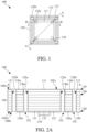
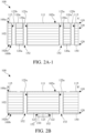
- FIGS. 1 and 2B are cross-sectional views of the substrate structure 100 along lines A-A' and B-B' shown in FIG. 1 , respectively, in accordance with some embodiments.
- the substrate structure 100 illustrated as a printed circuit board (PCB) and includes a build-up layer structure 102 having a first surface 102a (e.g., top surface) and a second surface 102b (e.g., bottom surface) opposite to the first surface 102a.
- a first surface 102a e.g., top surface
- second surface 102b e.g., bottom surface
- the substrate structure 100 further includes a solder mask (not shown) covering the first surface 102a of the build-up layer structure 102. In other embodiments, there is no solder mask disposed on the first surface 102a of the build-up layer structure 102, and the first surface 102a may serve as the top surface 100a of the substrate structure 100. Additionally, in some embodiments, the substrate structure 100 includes a solder mask 150 covering the second surface 102b of the build-up layer structure 102, and the bottom surface of the solder mask 150 may serve as the bottom surface 100b of the substrate structure 100.
- the build-up layer structure 102 may include a core substrate (not shown) and a plurality of alternating laminated conductive layers (not shown) and dielectric layers (not shown) stacked on opposite sides of the core substrate.
- the build-up layer structure 102 may be fabricated without the core substrate and include a plurality of alternating laminated conductive layers (not shown) and dielectric layers (not shown).
- the alternating laminated conductive layers include a conductive material, such as metals comprising copper, gold, silver, or other applicable metals.
- the dielectric layers include Pre-preg or other applicable dielectric materials.
- the build-up layer structure 102 may include at least four conductive layers (not shown) and four dielectric layers (not shown).
- the conductive layers of the build-up layer structure 102 layers may be served as pads, ground planes, traces and/or routing patterns for ground/signal/power.
- the uppermost conductive layer and/or lowermost conductive layer may include pads, ground traces, power traces and signal traces; other conductive layers between the uppermost conductive layer and the lowermost conductive layer may include ground traces, power traces and signal traces.
- the traces may include signal traces that are used for the input/output (I/O) connections of an overlying package assembly (not shown), and ground traces that are connected to the ground planes.
- the pads are connected to different terminals of the traces and used for the package that is mounted directly on them.
- the ground planes are grounded and connected to ground pads of the package assembly.
- the conductive layers may be made of metal, such as copper, the like, or another suitable conductive material.
- the build-up layer structure 102 of the substrate structure 100 may include a first conductive layer 110 and a second conductive layer 120.
- the first conductive layer 110 is adjacent to the first surface (top surface) 102a of the build-up layer structure 102 and the second conductive layer 120 is adjacent to the second surface 102b (bottom surface) of the build-up layer structure 102, as shown in FIGS. 2A and 2B .
- the build-up layer structure 102 of the substrate structure 100 may include additional conductive layers between the first conductive layer 110 and the second conductive layer 120, such as a conductive layer 130.
- the conductive layer 130 may be disposed above the second conductive layer 120 and below the first conductive layer 110.
- the first conductive layer 110 may be an uppermost conductive layer in the build-up layer structure 102 and exposed from the first surface 102a of the build-up layer structure 102.
- the first conductive layer 110 may be patterned to form pad pattern portions.
- the patterned first conductive layer 110 may include a chip pad portion 111, at least one thermal pad portion 113, and signal/power pad portions 115. That is, the chip pad portion 111, the at least one thermal pad portion 113 and the signal/power pad portions 115 are located at the same level in the build-up layer structure 102.
- the chip pad portion 111, the at least one thermal pad portion 113 and the signal/power pad portions 115 may be in the first conductive layer 110.
- the chip pad portion (such as first pad portion) 111 may have a rectangular shape with four corners (not limited to these embodiments) and arranged at a central portion of the first surface 102a of the build-up layer structure 102.
- the chip pad portion 111 is used for attaching an overlying IC chip (not shown).
- the at least one thermal pad portion (such as second pad portion) 113 is separated from the chip pad portion 111 and arranged near a corresponding corner of the chip pad portion 111.
- four thermal pad portions 113 are correspondingly arranged near the four corners of the chip pad portion 111.
- the thermal pad portions 113 serve as a portion of a heat dissipation structure with the chip pad portion 111.
- the thermal pad portions 113 also serve as ground pads in the package substrate 100.
- the chip pad portion 111 is used for thermal contact with the thermal pad of the IC chip for heat dissipation of the IC chip.
- the chip pad portion 111 is electrically insulated from the signal/power pad portions 115.
- the at least one thermal pad portion 113 may be located only near the corner(s) of the chip pad portion 111 and in a peripheral area of the chip pad chip pad portion 111.
- the number of thermal pad portions 113 can be one, two, three, or more.
- the number of thermal pad portions 113 may correspond to the number of corners of the chip pad portion 111, such as five or six.
- the embodiment uses a rectangular chip pad portion 111 as an example, which would result in four thermal pad portions 113.
- the first pad portion 111 is configured to bond with an exposed pad of the chip package.
- the signal/power pad portions 115 are also separated from the chip pad portion 111 and arranged along the edges of the chip pad portion 111.
- the signal/power pad portions 115 have a bar shape and arranged side-by-side and along four sides/edges of the chip pad portion 111 (not limited to these embodiments).
- each of the signal/power pad portions 115 has a smaller area than each of the thermal pad portions 113.
- the signal/power pad portions 115 serve as signal and/or power pads in the package substrate 100.
- each thermal pad portion 113 may be positioned between two adjacent groups of signal/power pad portions 115.
- One group of signal/power pad portions 115 is located along one side/edge of the periphery of the chip pad portion 111, and another group is situated along an adjacent side/edge.
- the second conductive layer 120 is located at a lower level in the build-up layer structure 102 than the first conductive layer 110.
- the second conductive layer 120 is a lowermost conductive layer in the build-up layer structure 102 and adjacent to the second surface 102b of the build-up layer structure102.
- the second conductive layer 120 is also patterned based on the design demands.
- the second conductive layer 120 includes ground traces 121, 122, and at least one power/signal trace 123.
- the ground traces 121, 122 serves as a portion of a heat dissipation structure and as an electrical ground layer in the substrate structure 100.
- the ground trace 121 and ground trace 122 are separated by the power/signal trace 123, so that the ground traces 121 and ground traces 122 are non-continuous structures.
- the substrate structure 100 further includes at least one first through-hole via (THV) 125a and at least one second THV 125b formed in the build-up layer structure 102.
- the at least one first THV 125a and the at least one second THV 125b pass though the build-up layer structure 102 (or the substrate structure 100).
- the at least one first THV 125a and the at least one second THV 125b extend from the first surface 102a of the build-up layer structure 102 to the second surface 102b of the build-up layer structure 102, so that the at least one first THV 125a and the at least one second THV 125b are exposed from the first surface 102a and the second surface 102b of the build-up layer structure 102.
- the at least one first THV 125a is positioned within the build-up layer structure 102 corresponding to the chip pad portion 111, as shown in FIG. 1 . In some embodiments, from a top view, the at least one first THV 125a is located within the region of the chip pad portion 111.
- each of the first THVs 125a passes through the chip pad portion 111 and the second conductive layer 120, and each of the first THVs 125a is surrounded by and in direct contact with the chip pad portion 111 and the second conductive layer 120, as shown in FIGS. 2A and 2B .
- FIG. 2A and 2B In FIG. 2A and 2B .
- each of the at least one first THV 125a and the at least one second THV 125b may be formed by plating a thin conductive layer on an inner sidewall of a through hole (not shown) passing through the build-up layer structure 102.
- each of the at least one first THV 125a and the at least one second THV 125b may be not filled with epoxy resin.
- the THVs may have a hollow pillar shape.
- the number, the shape, and the via size of the first THV 125a are based on the design demands and are not limited to these embodiments.
- two or more first THVs 125a with other shapes such as square, rectangular, triangular, oval, or polygon
- the number of the first THVs 125a can be one, two, three, or more.
- the number of the first THVs 125a may correspond to the number of corners of the chip pad portion 111, such as five or six; or the number of the first THVs 125a may greater than or less than the number of corners of the chip pad portion 111.
- each thermal pad portion 113 is disposed near the corner of the corresponding first THV 125a.
- the first THV 125a may be disposed adjacent to the corresponding thermal pad portion 113. Specifically, each thermal pad portion 113 is positioned at the corner closest to its corresponding first THV 125a, along with the second THV 125b that is associated with the same thermal pad portion 113.
- first THV 125a is located at the upper left corner of the chip pad portion 111
- second THV 125b would be located at the upper left corner of the corresponding thermal pad portion 113.
- the second THV 125b may only be associated with the thermal pad portion 113 at the upper left corner, while the other thermal pad portions 113 may not having a corresponding second THV 125b.
- the first THVs 125a and the second THVs 125b are arranged in a one-to-one correspondence, meaning that the quantity of each can be equal.
- the first THV(s) 125a may be located at any position of the chip pad portion 111 and is not limited to being located at a corner of the chip pad portion 111.
- the first THV(s) 125a may be located close to the edge of the chip pad portion 111 or located away from the edge of the chip pad portion 111, and so on.
- the position and quantity of the first THV(s) 125a can be freely designed according to requirements.
- the first THV(s) 125a can be connected to the corresponding second THV(s) 125b through the corresponding bridge trace(s).
- each of the second THVs 125b passes through and is surrounded by and in direct contact with the corresponding thermal pad portion 113, as shown in FIGS. 2A and 2B .
- four second THVs 125b with a circular/round shape are correspondingly arranged in the build-up layer structure 102 at the four thermal pad portions 113.
- the number, the shape, and the via size of the second THV 125b are based on the design demands and are not limited to these embodiments.
- two or more second THVs 125b with other shape may be arranged in the build-up layer structure 102 below a corresponding thermal pad portion 113.
- the first THVs 125a and the second THVs 125b serve as portions of a heat dissipation structure. Therefore, the first THVs 125a are also referred to as inner thermal THVs and the second THVs 125b are also referred to as outer thermal THVs.
- the thermal THVs may be made of metal (e.g., copper) or other suitable thermal conductive materials.
- the substrate structure 100 further includes at least one bridge trace that connects (or thermally connects) each first THV 125a to the corresponding second THV 125b.
- the at least one bridge trace may be formed in any one or more conductive layers of the build-up layer structure 102.
- the at least one bridge trace may be formed in the first conductive layer 110 (uppermost conductive layer), the second conductive layer 120 (lowermost conductive layer), and/or the conductive layer 130.
- Each of the bridge traces is thermally connected to and arranged between a corresponding first THV 125a and a corresponding second THV 125b.
- each of the bridge traces is in physical contact with the corresponding first THV 125a and the corresponding second THV 125b.
- the substrate structure 100 further includes bridge traces 110a, 120a and 130a to improve heat dissipation efficiency.
- the solder mask 150 has at least one opening 152 to expose at least a portion of the first THVs 125a and at least a portion of the second THVs 125b, as shown in FIG. 2A .
- the solder mask 150 may be a patterned solder mask (not limited to the embodiments). The at least one opening 152 of the solder mask 150 can further facilitate heat dissipation.
- the conductive connector 210 passes through the at least one opening 152, and the conductive connector 210 may span the power/signal trace 123 to connect the ground trace 121 and the ground trace 122. Since some or all of the separated ground traces are electrically connected together by the conductive connectors 210, the electrical ground traces can become more complete, so as to enhance the grounding performance thereof.
- the conductive connectors 210 are zero-ohm resistors or other suitable metal connecting components.
- FIG. 3 is a top view of an exemplary substrate structure 100' with a solder mask 150' in accordance with some embodiments
- FIG. 4 is a top view of an exemplary substrate structure 100" with a solder mask 150" in accordance with some embodiments.
- the substrate structure 100' has a structure/configuration similar to that of the substrate structure 100 shown in FIGS. 1, 2A and 2B .
- the substrate structure 100" also has a structure/configuration similar to that of the substrate structure 100 shown in FIGS. 1, 2A and 2B .
- the solder mask 150" has a plurality of openings 152", the plurality of openings 152" are separated from each other and arranged in a matrix, as viewed from a top-view perspective.
- the first THVs 125a and the second THVs 125b may entirely or partially exposed from the plurality of openings 152".
- at least one portion of the ground traces 121/122 is exposed by the plurality of openings 152".
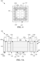
- the package assembly 500 includes a chip package 200 (which is also referred to as an IC chip) mounted on the substrate structure 100 (as shown in FIG. 2A ).
- the chip package 200 is also electrically connected to the signal/power pad portions 115 via leads 201 of the chip package 200.
- the chip package 200 is a QFN package that includes an exposed pad correspondingly bonded to the chip pad portion 111 of the substrate structure 100 for thermal conduction.
- the exposed pad of the chip package 200 is electrically insulated from the leads 201 of the chip package 200.
- the chip package 200 is a chip scale package (CSP) and is bond to the die pad portion 111 of the substrate structure 100.
- CSP chip scale package
- the package assembly 500 further includes one or more conductive connectors 210 electrically connected to the separated portions of the electrical ground trace (e.g., the ground trace 121 and the ground trace 122 of the second conductive layer 120) via the at least one opening of the solder mask 150.
- the electrical ground trace e.g., the ground trace 121 and the ground trace 122 of the second conductive layer 120
- the heat distribution on the ground trace 121 and the ground trace 122 may be unbalanced. Therefore, by connecting the two with the conductive connector 210, heat can be dissipated more evenly, thereby avoiding heat congestion and improving heat dissipation efficiency.
- the conductive connector 210 passes through the at least one opening, and the conductive connector 210 may span the power/signal trace 123 to connect the ground trace 121 and the ground trace 122. Since some or all of the separated ground traces are electrically connected together by the conductive connectors 210, the electrical ground traces can become more complete, so as to enhance the grounding performance thereof.
- the conductive connectors 210 are zero-ohm resistors or other suitable metal connecting components.
- the substrate structure is designed to fabricate a heat dissipation structure integrated into the substrate structure (e.g., PCB). More specifically, the heat dissipation structure is formed in an build-up layer structure of the substrate structure and at least includes a thermal pad arranged near to at least one corner of the chip pad, an outer thermal THV and an inner thermal THV respectively passes through the thermal pad and the chip pad, at least one conductive bridge layer that is connected between the outer thermal THV and the inner thermal THV, and an electrical ground layer thermally connected to the outer thermal THV and the inner thermal THV.
- the substrate structure e.g., PCB
- the conductive connectors e.g., zero-ohm resistors
- the conductive connectors are employed to connect the discontinuous ground layer in the substrate structure.
- the completeness of the ground layer can be increased, thereby enhancing the grounding performance and the heat dissipation efficiency.
Landscapes
- Engineering & Computer Science (AREA)
- Microelectronics & Electronic Packaging (AREA)
- Manufacturing & Machinery (AREA)
- Structure Of Printed Boards (AREA)
Abstract
Description
- This application claims the benefit of
U.S. Provisional Application No. 63/489,508 filed on March 10, 2023 - The present disclosure relates to a package technology, and in particular to through-hole vias formed at the corners of a substrate structure and a package assembly with the substrate structure.
- Technological advances in IC materials and design have produced generations of ICs where each generation has smaller and more complex circuits than the previous generation. In order to ensure the continued miniaturization and multi-functionality of electronic products and communication devices, semiconductor packages must be small in size, support multi-pin connection, operate at high speeds, and have high functionality. As a result, in the package assembly, more heat may be generated by the semiconductor chip or die.
- Accordingly, it is important to address the heat dissipation issue, in order to prevent damage to the electronic devices or the semiconductor chips/dies.
- In some embodiments, a substrate structure is provided. The substrate structure includes an uppermost conductive layer, a first through-hole via (THV) and a second THV, and a first bridge trace. The uppermost conductive layer is adjacent to the top surface of the substrate structure. The uppermost conductive layer includes a first pad portion and at least one second pad portion separated from the first pad portion and arranged near a corner of the first pad portion. The first THV and the second THV are formed in the substrate structure and pass through the substrate structure. The first THV passes through the first pad portion and the second THV passes through the least one second pad portion. The first bridge trace formed in the substrate structure and thermally connected to the second THV and the first THV.
- In some embodiments, a package assembly is provided. The package assembly includes a substrate structure and a chip package mounted on the substrate structure. The substrate structure includes an uppermost conductive layer, a first THV and a second THV, and a first bridge trace. The uppermost conductive layer is adjacent to the top surface of the substrate structure. The uppermost conductive layer includes a first pad portion and at least one second pad portion separated from the first pad portion and arranged near a corner of the first pad portion. The first THV and the second THV are formed in the substrate structure and pass through the substrate structure. The first THV passes through the first pad portion and the second THV passes through the least one second pad portion. The first bridge trace formed in the substrate structure and thermally connected to the second THV and the first THV
- A detailed description is given in the following embodiments with reference to the accompanying drawings.
- The present disclosure can be more fully understood by reading the subsequent detailed description and examples with references made to the accompanying drawings, wherein:
-
FIG. 1 is a top view of an exemplary substrate structure in accordance with some embodiments. -
FIG. 2A is a cross-sectional view of the substrate structure along line A-A' shown inFIG. 1 in accordance with some embodiments. -
FIG. 2A-1 is a cross-sectional view of the substrate structure along line A-A' shown inFIG. 1 in accordance with some embodiments. -
FIG. 2B is a cross-sectional view of the substrate structure along line B-B' shown inFIG. 1 in accordance with some embodiments. -
FIG. 2B-1 is a cross-sectional view of the substrate structure along line B-B' shown inFIG. 1 in accordance with some embodiments. -
FIG. 3 is a top view of an exemplary substrate structure with a solder mask in accordance with some embodiments. -
FIG. 4 is a top view of an exemplary substrate structure with a solder mask in accordance with some embodiments. -
FIG. 5A is a cross-sectional view of an exemplary package assembly with the substrate structure shown inFIG. 2A in accordance with some embodiments. -
FIG. 5B is a cross-sectional view of an exemplary package assembly with the substrate structure shown inFIG. 2B in accordance with some embodiments. - The following description is of the best-contemplated mode of carrying out the disclosure. This description is made for the purpose of illustrating the general principles of the disclosure and should not be taken in a limiting sense. The scope of the disclosure is determined by reference to the appended claims.
- The present disclosure will be described with respect to particular embodiments and with reference to certain drawings, but the disclosure is not limited thereto and is only limited by the claims. The drawings described are only schematic and are non-limiting. In the drawings, the size of some of the elements may be exaggerated for illustrative purposes and not drawn to scale. The dimensions and the relative dimensions do not correspond to actual dimensions in the practice of the disclosure.
- The present disclosure provides a substrate structure and a package assembly with the substrate structure. The package assembly includes at least one integrated circuit (IC) chip attached/mounted to a top surface of the substrate structure in, for example, a "Quad Flat No-lead (QFN)" configuration. The IC chip may be one of the many types of IC chips. For example, the IC chip may be a radio-frequency IC (RFIC) chip, a microprocessor chip, an application-specific integrated circuit (ASIC), or a memory chip according to various embodiments.
- In some embodiments, the substrate structure may include a core or coreless substrate that may be one of the different types of substrates known to those skilled in the relevant arts (e.g., organic or inorganic substrates). The core or coreless substrate may be made of one or more metal layers with one or more dielectric materials. Trace or routing patterns may be made in the metal layers by, for example, etching the metal layers. The core or coreless substrate may be a single-layer, a two-layer, or multi-layer substrate and may be formed of polypropylene (PP), Pre-preg, FR-4 and/or other epoxy laminate material.
- Refer to
FIGS. 1, 2A and2B , in whichFIG. 1 is a top view of anexemplary substrate structure 100 in accordance with some embodiments,FIGS. 2A and2B are cross-sectional views of thesubstrate structure 100 along lines A-A' and B-B' shown inFIG. 1 , respectively, in accordance with some embodiments. In some embodiments, thesubstrate structure 100 illustrated as a printed circuit board (PCB) and includes a build-up layer structure 102 having afirst surface 102a (e.g., top surface) and asecond surface 102b (e.g., bottom surface) opposite to thefirst surface 102a. In some embodiments, thesubstrate structure 100 further includes a solder mask (not shown) covering thefirst surface 102a of the build-uplayer structure 102. In other embodiments, there is no solder mask disposed on thefirst surface 102a of the build-uplayer structure 102, and thefirst surface 102a may serve as thetop surface 100a of thesubstrate structure 100. Additionally, in some embodiments, thesubstrate structure 100 includes asolder mask 150 covering thesecond surface 102b of the build-uplayer structure 102, and the bottom surface of thesolder mask 150 may serve as thebottom surface 100b of thesubstrate structure 100. In some embodiments, the build-uplayer structure 102 may include a core substrate (not shown) and a plurality of alternating laminated conductive layers (not shown) and dielectric layers (not shown) stacked on opposite sides of the core substrate. In some embodiments, the build-uplayer structure 102 may be fabricated without the core substrate and include a plurality of alternating laminated conductive layers (not shown) and dielectric layers (not shown). In some embodiments, the alternating laminated conductive layers include a conductive material, such as metals comprising copper, gold, silver, or other applicable metals. In some embodiments, the dielectric layers include Pre-preg or other applicable dielectric materials. In some embodiments, the build-uplayer structure 102 may include at least four conductive layers (not shown) and four dielectric layers (not shown). - In some embodiments, the conductive layers of the build-up
layer structure 102 layers may be served as pads, ground planes, traces and/or routing patterns for ground/signal/power. For example, the uppermost conductive layer and/or lowermost conductive layer may include pads, ground traces, power traces and signal traces; other conductive layers between the uppermost conductive layer and the lowermost conductive layer may include ground traces, power traces and signal traces. The traces may include signal traces that are used for the input/output (I/O) connections of an overlying package assembly (not shown), and ground traces that are connected to the ground planes. In some embodiments, the pads are connected to different terminals of the traces and used for the package that is mounted directly on them. Moreover, the ground planes are grounded and connected to ground pads of the package assembly. The conductive layers may be made of metal, such as copper, the like, or another suitable conductive material. In some embodiments, the build-uplayer structure 102 of thesubstrate structure 100 may include a firstconductive layer 110 and a secondconductive layer 120. The firstconductive layer 110 is adjacent to the first surface (top surface) 102a of the build-uplayer structure 102 and the secondconductive layer 120 is adjacent to thesecond surface 102b (bottom surface) of the build-uplayer structure 102, as shown inFIGS. 2A and2B . In some embodiments, the build-uplayer structure 102 of thesubstrate structure 100 may include additional conductive layers between the firstconductive layer 110 and the secondconductive layer 120, such as aconductive layer 130. Theconductive layer 130 may be disposed above the secondconductive layer 120 and below the firstconductive layer 110. - In some embodiments, the first
conductive layer 110 may be an uppermost conductive layer in the build-uplayer structure 102 and exposed from thefirst surface 102a of the build-uplayer structure 102. In some embodiments, the firstconductive layer 110 may be patterned to form pad pattern portions. For example, the patterned firstconductive layer 110 may include achip pad portion 111, at least onethermal pad portion 113, and signal/power pad portions 115. That is, thechip pad portion 111, the at least onethermal pad portion 113 and the signal/power pad portions 115 are located at the same level in the build-uplayer structure 102. In some embodiments, thechip pad portion 111, the at least onethermal pad portion 113 and the signal/power pad portions 115 may be in the firstconductive layer 110. - In some embodiments, the chip pad portion (such as first pad portion) 111 may have a rectangular shape with four corners (not limited to these embodiments) and arranged at a central portion of the
first surface 102a of the build-uplayer structure 102. Thechip pad portion 111 is used for attaching an overlying IC chip (not shown). The at least one thermal pad portion (such as second pad portion) 113 is separated from thechip pad portion 111 and arranged near a corresponding corner of thechip pad portion 111. InFIG. 1 , four thermal pad portions 113 (not limited to these embodiments) are correspondingly arranged near the four corners of thechip pad portion 111. Thethermal pad portions 113 serve as a portion of a heat dissipation structure with thechip pad portion 111. In addition, thethermal pad portions 113 also serve as ground pads in thepackage substrate 100. In some embodiments, thechip pad portion 111 is used for thermal contact with the thermal pad of the IC chip for heat dissipation of the IC chip. In addition, thechip pad portion 111 is electrically insulated from the signal/power pad portions 115. In some embodiments, the at least onethermal pad portion 113 may be located only near the corner(s) of thechip pad portion 111 and in a peripheral area of the chip padchip pad portion 111. In some embodiments, the number ofthermal pad portions 113 can be one, two, three, or more. In some embodiments, when the shape of thechip pad portion 111 is, for example, a pentagon or a hexagon, the number ofthermal pad portions 113 may correspond to the number of corners of thechip pad portion 111, such as five or six. For the sake of convenience in description, the embodiment uses a rectangularchip pad portion 111 as an example, which would result in fourthermal pad portions 113. In some embodiments, thefirst pad portion 111 is configured to bond with an exposed pad of the chip package. - In some embodiments, the signal/
power pad portions 115 are also separated from thechip pad portion 111 and arranged along the edges of thechip pad portion 111. InFIG. 1 , the signal/power pad portions 115 have a bar shape and arranged side-by-side and along four sides/edges of the chip pad portion 111 (not limited to these embodiments). Moreover, each of the signal/power pad portions 115 has a smaller area than each of thethermal pad portions 113. The signal/power pad portions 115 serve as signal and/or power pads in thepackage substrate 100. In some embodiments, eachthermal pad portion 113 may be positioned between two adjacent groups of signal/power pad portions 115. One group of signal/power pad portions 115 is located along one side/edge of the periphery of thechip pad portion 111, and another group is situated along an adjacent side/edge. - In some embodiments, the second
conductive layer 120 is located at a lower level in the build-uplayer structure 102 than the firstconductive layer 110. For example, the secondconductive layer 120 is a lowermost conductive layer in the build-uplayer structure 102 and adjacent to thesecond surface 102b of the build-up layer structure102. In some embodiments, the secondconductive layer 120 is also patterned based on the design demands. In some embodiments, the secondconductive layer 120 includes ground traces 121, 122, and at least one power/signal trace 123. The ground traces 121, 122 serves as a portion of a heat dissipation structure and as an electrical ground layer in thesubstrate structure 100. In some embodiments, theground trace 121 andground trace 122 are separated by the power/signal trace 123, so that the ground traces 121 and ground traces 122 are non-continuous structures. - In some embodiments, the
substrate structure 100 further includes at least one first through-hole via (THV) 125a and at least onesecond THV 125b formed in the build-uplayer structure 102. The at least onefirst THV 125a and the at least onesecond THV 125b pass though the build-up layer structure 102 (or the substrate structure 100). The at least onefirst THV 125a and the at least onesecond THV 125b extend from thefirst surface 102a of the build-uplayer structure 102 to thesecond surface 102b of the build-uplayer structure 102, so that the at least onefirst THV 125a and the at least onesecond THV 125b are exposed from thefirst surface 102a and thesecond surface 102b of the build-uplayer structure 102. The at least onefirst THV 125a is positioned within the build-uplayer structure 102 corresponding to thechip pad portion 111, as shown inFIG. 1 . In some embodiments, from a top view, the at least onefirst THV 125a is located within the region of thechip pad portion 111. In some embodiments, there are fourTHVs 125a disposed at the four corners of the rectangularchip pad portion 111. In some embodiments, at least onefirst THV 125a is not at the corner of thechip pad portion 125a. In other words, the first THV(s) 125a can be at any position of thechip pad portion 111, which is not limited by the present disclosure. Moreover, each of the first THVs 125a passes through thechip pad portion 111 and the secondconductive layer 120, and each of the first THVs 125a is surrounded by and in direct contact with thechip pad portion 111 and the secondconductive layer 120, as shown inFIGS. 2A and2B . InFIG. 1 , four first THVs 125a, each with a circular/round shape, are correspondingly positioned within the build-uplayer structure 102 at the four corners of thechip pad portion 111, of course, this is just an example, and the solution of the present disclosure is not limited to this. In some embodiments, each of the at least onefirst THV 125a and the at least onesecond THV 125b may be formed by plating a thin conductive layer on an inner sidewall of a through hole (not shown) passing through the build-uplayer structure 102. Furthermore, each of the at least onefirst THV 125a and the at least onesecond THV 125b may be not filled with epoxy resin. The THVs may have a hollow pillar shape. - However, the number, the shape, and the via size of the
first THV 125a are based on the design demands and are not limited to these embodiments. For example, two or morefirst THVs 125a with other shapes (such as square, rectangular, triangular, oval, or polygon) may be arranged in the build-uplayer structure 102 and in thechip pad portion 111. In some embodiments, the number of the first THVs 125a can be one, two, three, or more. In some embodiments, when the shape of thechip pad portion 111 is, for example, a pentagon or a hexagon, the number of the first THVs 125a may correspond to the number of corners of thechip pad portion 111, such as five or six; or the number of the first THVs 125a may greater than or less than the number of corners of thechip pad portion 111. - Moreover, similar to the first THVs 125a, the at least one
second THV 125b also extends from thefirst surface 102a of the build-uplayer structure 102 to thesecond surface 102b of the build-uplayer structure 102. In some embodiments, eachthermal pad portion 113 is disposed near the corner of the correspondingfirst THV 125a. In some embodiments, thefirst THV 125a may be disposed adjacent to the correspondingthermal pad portion 113. Specifically, eachthermal pad portion 113 is positioned at the corner closest to its correspondingfirst THV 125a, along with thesecond THV 125b that is associated with the samethermal pad portion 113. For example, if a singlefirst THV 125a is located at the upper left corner of thechip pad portion 111, then a singlesecond THV 125b would be located at the upper left corner of the correspondingthermal pad portion 113. It is possible for there to be multiplethermal pad portions 113; however, thesecond THV 125b may only be associated with thethermal pad portion 113 at the upper left corner, while the otherthermal pad portions 113 may not having a correspondingsecond THV 125b. In some embodiments, thefirst THVs 125a and thesecond THVs 125b are arranged in a one-to-one correspondence, meaning that the quantity of each can be equal. In some embodiments, there are foursecond THVs 125b corresponding to the four first THVs125a to improve heat dissipation efficiency. Each of thesecond THVs 125b is arranged in the build-uplayer structure 102 at a correspondingthermal pad portion 113, as shown inFIG. 1 . In some embodiments, the first THV(s) 125a may be located at any position of thechip pad portion 111 and is not limited to being located at a corner of thechip pad portion 111. For example, the first THV(s) 125a may be located close to the edge of thechip pad portion 111 or located away from the edge of thechip pad portion 111, and so on. The position and quantity of the first THV(s) 125a can be freely designed according to requirements. In addition, no matter where the first THV(s) 125a is located in thechip pad portion 111, it can be connected to the corresponding second THV(s) 125b through the corresponding bridge trace(s). Moreover, each of thesecond THVs 125b passes through and is surrounded by and in direct contact with the correspondingthermal pad portion 113, as shown inFIGS. 2A and2B . InFIG. 1 , foursecond THVs 125b with a circular/round shape are correspondingly arranged in the build-uplayer structure 102 at the fourthermal pad portions 113. However, the number, the shape, and the via size of thesecond THV 125b are based on the design demands and are not limited to these embodiments. For example, two or more second THVs 125b with other shape (such as square, rectangular, triangular, oval, or polygon) may be arranged in the build-uplayer structure 102 below a correspondingthermal pad portion 113. - In some embodiments, the
first THVs 125a and thesecond THVs 125b serve as portions of a heat dissipation structure. Therefore, the first THVs 125a are also referred to as inner thermal THVs and thesecond THVs 125b are also referred to as outer thermal THVs. The thermal THVs may be made of metal (e.g., copper) or other suitable thermal conductive materials. - In some embodiments, the
substrate structure 100 further includes at least one bridge trace that connects (or thermally connects) eachfirst THV 125a to the correspondingsecond THV 125b. In some embodiments, the at least one bridge trace may be formed in any one or more conductive layers of the build-uplayer structure 102. In some embodiments, the at least one bridge trace may be formed in the first conductive layer 110 (uppermost conductive layer), the second conductive layer 120 (lowermost conductive layer), and/or theconductive layer 130. Each of the bridge traces is thermally connected to and arranged between a correspondingfirst THV 125a and a correspondingsecond THV 125b. For example, each of the bridge traces is in physical contact with the correspondingfirst THV 125a and the correspondingsecond THV 125b. In some embodiments, thesubstrate structure 100 further includes bridge traces 110a, 120a and 130a to improve heat dissipation efficiency. - In some embodiments, the
solder mask 150 has at least oneopening 152 to expose at least a portion of thefirst THVs 125a and at least a portion of thesecond THVs 125b, as shown inFIG. 2A . In some embodiments, thesolder mask 150 may be a patterned solder mask (not limited to the embodiments). The at least oneopening 152 of thesolder mask 150 can further facilitate heat dissipation. - In some embodiments, one or more
conductive connectors 210 are electrically connected to the separated portions of the electrical ground trace (e.g., theground trace 121 and theground trace 122 of the second conductive layer 120) via the opening(s) 152 of thesolder mask 150. In some embodiments, as shown inFIGS. 2A and2B , because theground trace 121 and theground trace 122 are separated by power/signal trace 123 (e.g., making them non-continuous structures), the heat distribution on theground trace 121 and theground trace 122 may be unbalanced. Therefore, by connecting the two with theconductive connector 210, heat can be dissipated more evenly, thereby avoiding heat congestion and improving heat dissipation efficiency. In some embodiments, as shown inFIGS. 2A and2B , theconductive connector 210 passes through the at least oneopening 152, and theconductive connector 210 may span the power/signal trace 123 to connect theground trace 121 and theground trace 122. Since some or all of the separated ground traces are electrically connected together by theconductive connectors 210, the electrical ground traces can become more complete, so as to enhance the grounding performance thereof. In some embodiments, theconductive connectors 210 are zero-ohm resistors or other suitable metal connecting components. - In some other embodiments, due to the second
conductive layer 120 is patterned, the secondconductive layer 120 may not formed directly below thechip pad portion 111 corresponding to the line A-A' shown inFIG. 1 , as shown inFIG. 2A-1 . Similarly, the secondconductive layer 120 may not formed directly below thechip pad portion 111 corresponding to the line B-B' shown inFIG. 1 , as shown inFIG. 2B-1 . As shown inFIGS. 2A and2B , the ground traces 121, 122 of the patterned secondconductive layer 120 serve as the electrical ground layer, and the ground traces 121, 122 are two separate portions. The number of the separated portions of the patterned secondconductive layer 120 is based on design demands. In some embodiments, the at least oneopening 152 of thesolder mask 150 also exposes at least a portion of theground trace 121 and at least a portion of theground trace 122. - Refer to
FIGS. 3 and4 , in whichFIG. 3 is a top view of an exemplary substrate structure 100' with a solder mask 150' in accordance with some embodiments andFIG. 4 is a top view of anexemplary substrate structure 100" with asolder mask 150" in accordance with some embodiments. As shown inFIG. 3 , the substrate structure 100' has a structure/configuration similar to that of thesubstrate structure 100 shown inFIGS. 1, 2A and2B . Unlike thesolder mask 150 of thesubstrate structure 100, the solder mask 150' has a single large opening 152' that exposes portions of thesecond surface 102b corresponding to thechip pad portion 111, thethermal pad portions 113, thesecond THVs 125b, and the signal/power pad portions 115, as viewed from a top-view perspective. In some embodiments, thefirst THVs 125a and thesecond THVs 125b may entirely exposed from single large opening 152'. In some embodiments, at least one portion of the ground traces 121/122 is exposed by the single large opening 152'. In some embodiments, the ground traces 121/122 may be entirely exposed from the single large opening 152'. - As shown in
FIG. 4 , thesubstrate structure 100" also has a structure/configuration similar to that of thesubstrate structure 100 shown inFIGS. 1, 2A and2B . Unlike the solder mask 150' of the substrate structure 100', thesolder mask 150" has a plurality ofopenings 152", the plurality ofopenings 152" are separated from each other and arranged in a matrix, as viewed from a top-view perspective. In some embodiments, thefirst THVs 125a and thesecond THVs 125b may entirely or partially exposed from the plurality ofopenings 152". In some embodiments, at least one portion of the ground traces 121/122 is exposed by the plurality ofopenings 152". In some embodiments, the openings in the solder mask may vary in shape and arrangement. The embodiments described above are merely examples and do not limit the scope of the disclosure. In some embodiments, the openings (openings 152") in the solder mask layer expose at least a portion of the THVs (THV 125a and/orTHV 125b) and/or at least a portion of the ground traces (ground trace 121 and/or ground trace 122), thereby enhancing heat dissipation efficiency. - Refer to
FIGS. 5A and5B , in which 5A and 5B are cross-sectional views of an exemplary package assembly 500 with thesubstrate structure 100 shown inFIGS. 2A and2B , respectively, in accordance with some embodiments. As shown inFIGS. 5A and5B , the package assembly 500 includes a chip package 200 (which is also referred to as an IC chip) mounted on the substrate structure 100 (as shown inFIG. 2A ). Thechip package 200 is also electrically connected to the signal/power pad portions 115 vialeads 201 of thechip package 200. In some embodiments, thechip package 200 is a QFN package that includes an exposed pad correspondingly bonded to thechip pad portion 111 of thesubstrate structure 100 for thermal conduction. In some other embodiments, the exposed pad of thechip package 200 is electrically insulated from theleads 201 of thechip package 200. In some other embodiments, thechip package 200 is a chip scale package (CSP) and is bond to thedie pad portion 111 of thesubstrate structure 100. - In some embodiments, the package assembly 500 further includes one or more
conductive connectors 210 electrically connected to the separated portions of the electrical ground trace (e.g., theground trace 121 and theground trace 122 of the second conductive layer 120) via the at least one opening of thesolder mask 150. In some embodiments, as shown inFIGS. 5A and5B , because theground trace 121 and theground trace 122 are separated by power/signal trace 123 (e.g., making them non-continuous structures), the heat distribution on theground trace 121 and theground trace 122 may be unbalanced. Therefore, by connecting the two with theconductive connector 210, heat can be dissipated more evenly, thereby avoiding heat congestion and improving heat dissipation efficiency. In some embodiments, as shown inFIGS. 5A and5B , theconductive connector 210 passes through the at least one opening, and theconductive connector 210 may span the power/signal trace 123 to connect theground trace 121 and theground trace 122. Since some or all of the separated ground traces are electrically connected together by theconductive connectors 210, the electrical ground traces can become more complete, so as to enhance the grounding performance thereof. In some embodiments, theconductive connectors 210 are zero-ohm resistors or other suitable metal connecting components. - According to the foregoing embodiments, the substrate structure is designed to fabricate a heat dissipation structure integrated into the substrate structure (e.g., PCB). More specifically, the heat dissipation structure is formed in an build-up layer structure of the substrate structure and at least includes a thermal pad arranged near to at least one corner of the chip pad, an outer thermal THV and an inner thermal THV respectively passes through the thermal pad and the chip pad, at least one conductive bridge layer that is connected between the outer thermal THV and the inner thermal THV, and an electrical ground layer thermally connected to the outer thermal THV and the inner thermal THV. The heat dissipation structure allows the package assembly to effectively conduct the heat from the chip package mounted on the top of the substrate structure to the bottom of the substrate structure. Furthermore, the solder mask formed on the bottom of the substrate structure has openings to facilitate heat dissipation. As a result, the heat dissipation efficiency can be increased.
- According to the foregoing embodiments, the conductive connectors (e.g., zero-ohm resistors) are employed to connect the discontinuous ground layer in the substrate structure. As a result, the completeness of the ground layer can be increased, thereby enhancing the grounding performance and the heat dissipation efficiency.
- While the disclosure has been described by way of example and in terms of the preferred embodiments, it should be understood that the disclosure is not limited to the disclosed embodiments. On the contrary, it is intended to cover various modifications and similar arrangements (as would be apparent to those skilled in the art). Therefore, the scope of the appended claims should be accorded the broadest interpretation so as to encompass all such modifications and similar arrangements.
Claims (11)
- A substrate structure (100, 100'), comprising:an uppermost conductive layer (110) adjacent to a top surface (100a) of the substrate structure (100, 100'), wherein the uppermost conductive layer (110) comprises:a first pad portion (111); andat least one second pad portion (113) separated from the first pad portion (111) and arranged near a corner of the first pad portion (111);a first through-hole via, THV, and a second THV (125b) formed in the substrate structure (100, 100') and passing through the substrate structure (100, 100'), wherein the first THV (125a) passes through the first pad portion (111) and the second THV (125b) passes through the least one second pad portion (113); anda first bridge trace (110a, 120a, 130a) formed in the substrate structure (100, 100') and thermally connected to the second THV (125b) and the first THV (125a).
- The substrate structure (100, 100') as claimed in claim 1, wherein the first bridge trace (110a, 120a, 130a) is formed in the uppermost conductive layer (110) or in another conductive layer (120, 130) of the substrate structure (100, 100') that is below the uppermost conductive layer (110).
- The substrate structure (100, 100') as claimed in claim 2, further comprising: a second bridge trace (120a, 130a) thermally connected to the second THV (125b) and the first THV (125a), and formed in a conductive layer (120, 130) of the substrate structure (100, 100') that is different from the conductive layer (110) in which the first bridge trace is (110a) formed.
- The substrate structure (100, 100') as claimed in claim 1, further comprising:a lowermost conductive layer (120) adjacent to a bottom surface (100b) of the substrate structure (100, 100'); anda solder mask (150, 150', 150") layer disposed on the lowermost conductive layer (120), and comprising at least one opening (152, 152', 152") to expose at least a portion of the second THV (125b) and at least a portion of the first THV (125a).
- The substrate structure (100, 100') as claimed in claim 4, wherein the lowermost conductive layer (120) comprises a first ground trace (121, 122), wherein the at least one opening (152, 152', 152") further exposes at least a portion of the first ground trace (121, 122).
- The substrate structure (100, 100') as claimed in claim 5, wherein the lowermost conductive layer (120) further comprises a power/signal trace (123) and a second ground trace (121, 122) separated from the first ground trace (121, 122) by the power/signal trace (123), wherein the power/signal trace (123) is covered by the solder mask (150, 150', 150") layer, and at least a portion of the second ground trace (121, 122) is exposed from the at least one opening (152, 152', 152").
- The substrate structure (100, 100') as claimed in claim 6, further comprising:a conductive connector (210) electrically coupling the first ground trace (121, 122) and the second ground trace (121, 122),wherein the conductive connector (210) passes through the at least one opening (152, 152', 152"), and further spans the power/signal trace (123).
- The substrate structure (100, 100') as claimed in claim 1, wherein the first bridge trace (1 10a, 120a, 130a) is connected to an electrical ground layer in the substrate structure (100, 100').
- The substrate structure (100, 100') as claimed in claim 4, wherein the at least one opening (152, 152', 152") is a single opening (152') that entirely exposes the second THV (125b) and the first THV (125a).
- The substrate structure (100, 100') as claimed in claim 4, wherein the solder mask (150, 150', 150") layer includes a plurality of openings (152") that are spaced apart from each other to form a matrix of openings (152").
- A package assembly (500), comprising:a substrate structure (100, 100') of any one of claims 1 to 10; anda chip package (200) mounted on the substrate structure (100, 100').
Applications Claiming Priority (2)
| Application Number | Priority Date | Filing Date | Title |
|---|---|---|---|
| US202363489508P | 2023-03-10 | 2023-03-10 | |
| US18/594,573 US20240304534A1 (en) | 2023-03-10 | 2024-03-04 | Thermally improved substrate structure and package assembly with the same |
Publications (2)
| Publication Number | Publication Date |
|---|---|
| EP4429413A1 true EP4429413A1 (en) | 2024-09-11 |
| EP4429413B1 EP4429413B1 (en) | 2025-12-10 |
Family
ID=90363540
Family Applications (1)
| Application Number | Title | Priority Date | Filing Date |
|---|---|---|---|
| EP24162136.6A Active EP4429413B1 (en) | 2023-03-10 | 2024-03-07 | Thermally improved substrate structure and package assembly with the same |
Country Status (2)
| Country | Link |
|---|---|
| US (1) | US20240304534A1 (en) |
| EP (1) | EP4429413B1 (en) |
Citations (5)
| Publication number | Priority date | Publication date | Assignee | Title |
|---|---|---|---|---|
| US20030136582A1 (en) * | 2002-01-18 | 2003-07-24 | Sheng-Tsung Liu | Substrate board structure |
| US20150092374A1 (en) * | 2013-10-02 | 2015-04-02 | International Business Machines Corporation | Solder void reduction between electronic packages and printed circuit boards |
| US20170290158A1 (en) * | 2016-03-30 | 2017-10-05 | Intel Corporation | Surface-mountable power delivery bus board |
| JP6699535B2 (en) * | 2016-12-14 | 2020-05-27 | 株式会社デンソー | Circuit board |
| US20220059427A1 (en) * | 2020-08-21 | 2022-02-24 | Murata Manufacturing Co., Ltd. | Semiconductor package, semiconductor device, semiconductor package-mounted apparatus, and semiconductor device-mounted apparatus |
-
2024
- 2024-03-04 US US18/594,573 patent/US20240304534A1/en active Pending
- 2024-03-07 EP EP24162136.6A patent/EP4429413B1/en active Active
Patent Citations (5)
| Publication number | Priority date | Publication date | Assignee | Title |
|---|---|---|---|---|
| US20030136582A1 (en) * | 2002-01-18 | 2003-07-24 | Sheng-Tsung Liu | Substrate board structure |
| US20150092374A1 (en) * | 2013-10-02 | 2015-04-02 | International Business Machines Corporation | Solder void reduction between electronic packages and printed circuit boards |
| US20170290158A1 (en) * | 2016-03-30 | 2017-10-05 | Intel Corporation | Surface-mountable power delivery bus board |
| JP6699535B2 (en) * | 2016-12-14 | 2020-05-27 | 株式会社デンソー | Circuit board |
| US20220059427A1 (en) * | 2020-08-21 | 2022-02-24 | Murata Manufacturing Co., Ltd. | Semiconductor package, semiconductor device, semiconductor package-mounted apparatus, and semiconductor device-mounted apparatus |
Also Published As
| Publication number | Publication date |
|---|---|
| EP4429413B1 (en) | 2025-12-10 |
| US20240304534A1 (en) | 2024-09-12 |
Similar Documents
| Publication | Publication Date | Title |
|---|---|---|
| CN1282244C (en) | Electronic module with three-dimensional array of carrier-mounted integrated circuit packages | |
| US5467252A (en) | Method for plating using nested plating buses and semiconductor device having the same | |
| US5563446A (en) | Surface mount peripheral leaded and ball grid array package | |
| US7968991B2 (en) | Stacked package module and board having exposed ends | |
| US6331939B1 (en) | Stackable ball grid array package | |
| EP3416190B1 (en) | Package-on-package assembly with wire bond vias | |
| US5386141A (en) | Leadframe having one or more power/ground planes without vias | |
| US6552416B1 (en) | Multiple die lead frame package with enhanced die-to-die interconnect routing using internal lead trace wiring | |
| KR970003991B1 (en) | Double-sided memory board and memory module using it | |
| CN101350318B (en) | Electronic package and electronic device | |
| CN1396799A (en) | Printed circuit board with improved pad structure | |
| JPH1168026A (en) | Wiring auxiliary package and printed circuit board structure | |
| US6225687B1 (en) | Chip package with degassing holes | |
| US7180182B2 (en) | Semiconductor component | |
| KR20240074215A (en) | Semiconductor package | |
| US5818102A (en) | System having integrated circuit package with lead frame having internal power and ground busses | |
| JP3016910B2 (en) | Semiconductor module structure | |
| US5691569A (en) | Integrated circuit package that has a plurality of staggered pins | |
| KR20240152586A (en) | Semiconductor package | |
| JPH11289029A (en) | Plastic package for semiconductor device | |
| US6103548A (en) | Semiconductor device and method of manufacture | |
| EP4429413B1 (en) | Thermally improved substrate structure and package assembly with the same | |
| EP3182449A1 (en) | Semiconductor package | |
| US20030080418A1 (en) | Semiconductor device having power supply pads arranged between signal pads and substrate edge | |
| KR100725517B1 (en) | Multi-layer wiring board having bonding pads and ball lands formed in a plurality of layers and semiconductor package structure using the same |
Legal Events
| Date | Code | Title | Description |
|---|---|---|---|
| PUAI | Public reference made under article 153(3) epc to a published international application that has entered the european phase |
Free format text: ORIGINAL CODE: 0009012 |
|
| STAA | Information on the status of an ep patent application or granted ep patent |
Free format text: STATUS: THE APPLICATION HAS BEEN PUBLISHED |
|
| AK | Designated contracting states |
Kind code of ref document: A1 Designated state(s): AL AT BE BG CH CY CZ DE DK EE ES FI FR GB GR HR HU IE IS IT LI LT LU LV MC ME MK MT NL NO PL PT RO RS SE SI SK SM TR |
|
| STAA | Information on the status of an ep patent application or granted ep patent |
Free format text: STATUS: REQUEST FOR EXAMINATION WAS MADE |
|
| 17P | Request for examination filed |
Effective date: 20250305 |
|
| GRAP | Despatch of communication of intention to grant a patent |
Free format text: ORIGINAL CODE: EPIDOSNIGR1 |
|
| STAA | Information on the status of an ep patent application or granted ep patent |
Free format text: STATUS: GRANT OF PATENT IS INTENDED |
|
| INTG | Intention to grant announced |
Effective date: 20250701 |
|
| RAP3 | Party data changed (applicant data changed or rights of an application transferred) |
Owner name: MEDIATEK INC. |
|
| GRAS | Grant fee paid |
Free format text: ORIGINAL CODE: EPIDOSNIGR3 |
|
| GRAA | (expected) grant |
Free format text: ORIGINAL CODE: 0009210 |
|
| STAA | Information on the status of an ep patent application or granted ep patent |
Free format text: STATUS: THE PATENT HAS BEEN GRANTED |
|
| AK | Designated contracting states |
Kind code of ref document: B1 Designated state(s): AL AT BE BG CH CY CZ DE DK EE ES FI FR GB GR HR HU IE IS IT LI LT LU LV MC ME MK MT NL NO PL PT RO RS SE SI SK SM TR |
|
| REG | Reference to a national code |
Ref country code: CH Ref legal event code: F10 Free format text: ST27 STATUS EVENT CODE: U-0-0-F10-F00 (AS PROVIDED BY THE NATIONAL OFFICE) Effective date: 20251210 Ref country code: GB Ref legal event code: FG4D |
|
| REG | Reference to a national code |
Ref country code: DE Ref legal event code: R096 Ref document number: 602024001565 Country of ref document: DE |
|
| REG | Reference to a national code |
Ref country code: IE Ref legal event code: FG4D |
|
| PG25 | Lapsed in a contracting state [announced via postgrant information from national office to epo] |
Ref country code: ES Free format text: LAPSE BECAUSE OF FAILURE TO SUBMIT A TRANSLATION OF THE DESCRIPTION OR TO PAY THE FEE WITHIN THE PRESCRIBED TIME-LIMIT Effective date: 20251210 |
|
| REG | Reference to a national code |
Ref country code: LT Ref legal event code: MG9D |
|
| PG25 | Lapsed in a contracting state [announced via postgrant information from national office to epo] |
Ref country code: NO Free format text: LAPSE BECAUSE OF FAILURE TO SUBMIT A TRANSLATION OF THE DESCRIPTION OR TO PAY THE FEE WITHIN THE PRESCRIBED TIME-LIMIT Effective date: 20260310 |
|
| PG25 | Lapsed in a contracting state [announced via postgrant information from national office to epo] |
Ref country code: HR Free format text: LAPSE BECAUSE OF FAILURE TO SUBMIT A TRANSLATION OF THE DESCRIPTION OR TO PAY THE FEE WITHIN THE PRESCRIBED TIME-LIMIT Effective date: 20251210 Ref country code: FI Free format text: LAPSE BECAUSE OF FAILURE TO SUBMIT A TRANSLATION OF THE DESCRIPTION OR TO PAY THE FEE WITHIN THE PRESCRIBED TIME-LIMIT Effective date: 20251210 |
|
| PGFP | Annual fee paid to national office [announced via postgrant information from national office to epo] |
Ref country code: AT Payment date: 20260301 Year of fee payment: 3 |
|
| REG | Reference to a national code |
Ref country code: NL Ref legal event code: MP Effective date: 20251210 |
|
| PG25 | Lapsed in a contracting state [announced via postgrant information from national office to epo] |
Ref country code: RS Free format text: LAPSE BECAUSE OF FAILURE TO SUBMIT A TRANSLATION OF THE DESCRIPTION OR TO PAY THE FEE WITHIN THE PRESCRIBED TIME-LIMIT Effective date: 20260310 |
|
| PGFP | Annual fee paid to national office [announced via postgrant information from national office to epo] |
Ref country code: FR Payment date: 20260212 Year of fee payment: 3 |
|
| PG25 | Lapsed in a contracting state [announced via postgrant information from national office to epo] |
Ref country code: LV Free format text: LAPSE BECAUSE OF FAILURE TO SUBMIT A TRANSLATION OF THE DESCRIPTION OR TO PAY THE FEE WITHIN THE PRESCRIBED TIME-LIMIT Effective date: 20251210 |
|
| PG25 | Lapsed in a contracting state [announced via postgrant information from national office to epo] |
Ref country code: BG Free format text: LAPSE BECAUSE OF FAILURE TO SUBMIT A TRANSLATION OF THE DESCRIPTION OR TO PAY THE FEE WITHIN THE PRESCRIBED TIME-LIMIT Effective date: 20251210 |