EP4429099A1 - Arrangement for current sharing of parallel-connected inverters - Google Patents
Arrangement for current sharing of parallel-connected inverters Download PDFInfo
- Publication number
- EP4429099A1 EP4429099A1 EP23161227.6A EP23161227A EP4429099A1 EP 4429099 A1 EP4429099 A1 EP 4429099A1 EP 23161227 A EP23161227 A EP 23161227A EP 4429099 A1 EP4429099 A1 EP 4429099A1
- Authority
- EP
- European Patent Office
- Prior art keywords
- parallel
- commutation
- inverter
- leg
- connected inverter
- Prior art date
- Legal status (The legal status is an assumption and is not a legal conclusion. Google has not performed a legal analysis and makes no representation as to the accuracy of the status listed.)
- Granted
Links
Images



Classifications
-
- H—ELECTRICITY
- H02—GENERATION; CONVERSION OR DISTRIBUTION OF ELECTRIC POWER
- H02M—APPARATUS FOR CONVERSION BETWEEN AC AND AC, BETWEEN AC AND DC, OR BETWEEN DC AND DC, AND FOR USE WITH MAINS OR SIMILAR POWER SUPPLY SYSTEMS; CONVERSION OF DC OR AC INPUT POWER INTO SURGE OUTPUT POWER; CONTROL OR REGULATION THEREOF
- H02M7/00—Conversion of AC power input into DC power output; Conversion of DC power input into AC power output
- H02M7/42—Conversion of DC power input into AC power output without possibility of reversal
- H02M7/44—Conversion of DC power input into AC power output without possibility of reversal by static converters
- H02M7/48—Conversion of DC power input into AC power output without possibility of reversal by static converters using discharge tubes with control electrode or semiconductor devices with control electrode
- H02M7/493—Conversion of DC power input into AC power output without possibility of reversal by static converters using discharge tubes with control electrode or semiconductor devices with control electrode the static converters being arranged for operation in parallel
-
- H—ELECTRICITY
- H02—GENERATION; CONVERSION OR DISTRIBUTION OF ELECTRIC POWER
- H02M—APPARATUS FOR CONVERSION BETWEEN AC AND AC, BETWEEN AC AND DC, OR BETWEEN DC AND DC, AND FOR USE WITH MAINS OR SIMILAR POWER SUPPLY SYSTEMS; CONVERSION OF DC OR AC INPUT POWER INTO SURGE OUTPUT POWER; CONTROL OR REGULATION THEREOF
- H02M1/00—Details of apparatus for conversion
- H02M1/0003—Details of control, feedback or regulation circuits
- H02M1/0009—Devices or circuits for detecting current in a converter
-
- H—ELECTRICITY
- H02—GENERATION; CONVERSION OR DISTRIBUTION OF ELECTRIC POWER
- H02M—APPARATUS FOR CONVERSION BETWEEN AC AND AC, BETWEEN AC AND DC, OR BETWEEN DC AND DC, AND FOR USE WITH MAINS OR SIMILAR POWER SUPPLY SYSTEMS; CONVERSION OF DC OR AC INPUT POWER INTO SURGE OUTPUT POWER; CONTROL OR REGULATION THEREOF
- H02M1/00—Details of apparatus for conversion
- H02M1/08—Circuits specially adapted for the generation of control voltages for semiconductor devices incorporated in static converters
- H02M1/088—Circuits specially adapted for the generation of control voltages for semiconductor devices incorporated in static converters for the simultaneous control of series or parallel connected semiconductor devices
-
- H—ELECTRICITY
- H02—GENERATION; CONVERSION OR DISTRIBUTION OF ELECTRIC POWER
- H02M—APPARATUS FOR CONVERSION BETWEEN AC AND AC, BETWEEN AC AND DC, OR BETWEEN DC AND DC, AND FOR USE WITH MAINS OR SIMILAR POWER SUPPLY SYSTEMS; CONVERSION OF DC OR AC INPUT POWER INTO SURGE OUTPUT POWER; CONTROL OR REGULATION THEREOF
- H02M7/00—Conversion of AC power input into DC power output; Conversion of DC power input into AC power output
- H02M7/42—Conversion of DC power input into AC power output without possibility of reversal
- H02M7/44—Conversion of DC power input into AC power output without possibility of reversal by static converters
- H02M7/48—Conversion of DC power input into AC power output without possibility of reversal by static converters using discharge tubes with control electrode or semiconductor devices with control electrode
- H02M7/53—Conversion of DC power input into AC power output without possibility of reversal by static converters using discharge tubes with control electrode or semiconductor devices with control electrode using devices of a triode or transistor type requiring continuous application of a control signal
- H02M7/537—Conversion of DC power input into AC power output without possibility of reversal by static converters using discharge tubes with control electrode or semiconductor devices with control electrode using devices of a triode or transistor type requiring continuous application of a control signal using semiconductor devices only, e.g. single switched pulse inverters
- H02M7/5387—Conversion of DC power input into AC power output without possibility of reversal by static converters using discharge tubes with control electrode or semiconductor devices with control electrode using devices of a triode or transistor type requiring continuous application of a control signal using semiconductor devices only, e.g. single switched pulse inverters in a bridge configuration
-
- H—ELECTRICITY
- H02—GENERATION; CONVERSION OR DISTRIBUTION OF ELECTRIC POWER
- H02M—APPARATUS FOR CONVERSION BETWEEN AC AND AC, BETWEEN AC AND DC, OR BETWEEN DC AND DC, AND FOR USE WITH MAINS OR SIMILAR POWER SUPPLY SYSTEMS; CONVERSION OF DC OR AC INPUT POWER INTO SURGE OUTPUT POWER; CONTROL OR REGULATION THEREOF
- H02M7/00—Conversion of AC power input into DC power output; Conversion of DC power input into AC power output
- H02M7/42—Conversion of DC power input into AC power output without possibility of reversal
- H02M7/44—Conversion of DC power input into AC power output without possibility of reversal by static converters
- H02M7/48—Conversion of DC power input into AC power output without possibility of reversal by static converters using discharge tubes with control electrode or semiconductor devices with control electrode
- H02M7/53—Conversion of DC power input into AC power output without possibility of reversal by static converters using discharge tubes with control electrode or semiconductor devices with control electrode using devices of a triode or transistor type requiring continuous application of a control signal
- H02M7/537—Conversion of DC power input into AC power output without possibility of reversal by static converters using discharge tubes with control electrode or semiconductor devices with control electrode using devices of a triode or transistor type requiring continuous application of a control signal using semiconductor devices only, e.g. single switched pulse inverters
- H02M7/5387—Conversion of DC power input into AC power output without possibility of reversal by static converters using discharge tubes with control electrode or semiconductor devices with control electrode using devices of a triode or transistor type requiring continuous application of a control signal using semiconductor devices only, e.g. single switched pulse inverters in a bridge configuration
- H02M7/53871—Conversion of DC power input into AC power output without possibility of reversal by static converters using discharge tubes with control electrode or semiconductor devices with control electrode using devices of a triode or transistor type requiring continuous application of a control signal using semiconductor devices only, e.g. single switched pulse inverters in a bridge configuration with automatic control of output voltage or current
-
- H—ELECTRICITY
- H02—GENERATION; CONVERSION OR DISTRIBUTION OF ELECTRIC POWER
- H02M—APPARATUS FOR CONVERSION BETWEEN AC AND AC, BETWEEN AC AND DC, OR BETWEEN DC AND DC, AND FOR USE WITH MAINS OR SIMILAR POWER SUPPLY SYSTEMS; CONVERSION OF DC OR AC INPUT POWER INTO SURGE OUTPUT POWER; CONTROL OR REGULATION THEREOF
- H02M1/00—Details of apparatus for conversion
- H02M1/0003—Details of control, feedback or regulation circuits
- H02M1/0025—Arrangements for modifying reference values, feedback values or error values in the control loop of a converter
-
- H—ELECTRICITY
- H02—GENERATION; CONVERSION OR DISTRIBUTION OF ELECTRIC POWER
- H02M—APPARATUS FOR CONVERSION BETWEEN AC AND AC, BETWEEN AC AND DC, OR BETWEEN DC AND DC, AND FOR USE WITH MAINS OR SIMILAR POWER SUPPLY SYSTEMS; CONVERSION OF DC OR AC INPUT POWER INTO SURGE OUTPUT POWER; CONTROL OR REGULATION THEREOF
- H02M7/00—Conversion of AC power input into DC power output; Conversion of DC power input into AC power output
- H02M7/42—Conversion of DC power input into AC power output without possibility of reversal
- H02M7/44—Conversion of DC power input into AC power output without possibility of reversal by static converters
- H02M7/48—Conversion of DC power input into AC power output without possibility of reversal by static converters using discharge tubes with control electrode or semiconductor devices with control electrode
- H02M7/505—Conversion of DC power input into AC power output without possibility of reversal by static converters using discharge tubes with control electrode or semiconductor devices with control electrode using devices of a thyratron or thyristor type requiring extinguishing means
- H02M7/515—Conversion of DC power input into AC power output without possibility of reversal by static converters using discharge tubes with control electrode or semiconductor devices with control electrode using devices of a thyratron or thyristor type requiring extinguishing means using semiconductor devices only
- H02M7/521—Conversion of DC power input into AC power output without possibility of reversal by static converters using discharge tubes with control electrode or semiconductor devices with control electrode using devices of a thyratron or thyristor type requiring extinguishing means using semiconductor devices only in a bridge configuration
Definitions
- the present invention relates to parallel-connected power inverters, and more particularly to a current sharing of parallel-connected power inverters.
- a dc-ac converter also known as an inverter, converts dc power to ac power at desired output voltage and output frequency.
- the inverter therefore can be operated as an adjustable-frequency voltage source.
- the dc power input to the inverter may be obtained from an existing power supply network through a rectifier or from a battery, fuel cell, photovoltaic array, etc.
- the filter capacitor(s) across the input terminals of the inverter provides a fairly constant dc-link voltage.
- a configuration of ac to dc converter and dc to ac inverter may be called a dc-link converter.
- a power inverter with an increased output power capability is implemented by connecting a plurality of inverter units in parallel with one another to feed the same load through output reactors.
- the parallel-connected inverter units may receive simultaneous and similar control signals to provide a desired output of the power inverter.
- the currents between the units can be unequal in magnitude. Such a current imbalance can stress the components unevenly and wear switch components with higher current prematurely. A higher current in a switch component can result in a higher dissipated power and, further, a higher temperature of the component.
- the control pulses can be modified by delaying a turn-on time instant for a switch that has the highest current or by delaying turn-off time instants for a switch that has the smallest current.
- One such method is disclosed in EP0524398 .
- the conducting times of the parallel components are modified to equalize stresses to the switch components on the basis of measured inverter unit currents.
- US8432714 discloses a method for balancing load between parallel-connected inverters wherein temperatures of each output leg of each inverter are determined and the switching instructions for one or more of the parallel inverters are modified for controlling the temperatures of the output legs.
- WO2017079125A1 discloses a method wherein the output voltages of all the parallel connected power devices are measured, and the measuring results are used for mitigating timing differences during output voltage state changes caused e.g. by gate driver circuit and switching component parameter tolerances.
- US7068525 discloses a method of operating multiple parallel-connected inverters by regulating the individual currents of the inverters separately.
- An object of the present invention is to provide an improved power inverter system having two or more parallel-connected inverter legs.
- the power inverter system is recited in the independent claim 1. Preferred embodiments are disclosed in the dependent claims.
- An aspect of the invention is a power inverter system, comprising
- control arrangement if a sign of the difference between the pre-commutation and the post-commutation current values is negative, the control arrangement is configured to adjust switching instants for subsequent commutation so as to increase the negative difference towards zero, and wherein, if a sign of the difference between the pre-commutation and the post-commutation current values is positive, the control arrangement is configured to adjust switching instants for subsequent commutation so as to decrease the positive difference towards zero.
- the sign of the difference between the pre-commutation and the post-commutation current values indicates whether the switching instant of the parallel-connected inverter leg is earlier or later relative to a corresponding switching instant of at least one of the other parallel-connected inverter legs, and wherein the control arrangement is configured to advance the switching instants of the main switch, if the sign of the difference between the pre-commutation and the post-commutation current values indicates the switching instant of the parallel-connected inverter leg is later relative to a corresponding switching instants of at least one other parallel-connected inverter leg.
- An another aspect of the invention is a power inverter system, comprising
- the integral of the sensed voltage pulse represents a magnitude of the commutation-induced current difference in the parallel-connected inverter leg.
- the duration of the sensed voltage pulse represents a timing difference of a switching instant of the parallel-connected inverter leg relative to a corresponding switching instant of at least one other parallel-connected inverter leg.
- the sign of the sensed voltage pulse indicates whether the switching instant of the parallel-connected inverter leg is earlier or later relative to a corresponding switching instant of at least one other parallel-connected inverter leg.
- control arrangement is configured to advance the switching instant of the parallel-connected inverter leg, if the sign of the voltage pulse indicates the switching instant of the parallel-connected inverter leg is later relative to a corresponding switching instant of at least one other parallel-connected inverter leg; and wherein the control arrangement is configured to delay the switching instant of the parallel-connected inverter leg, if the sign of the voltage pulse indicates the switching instant of the parallel-connected inverter leg is earlier relative to a corresponding switching instant of at least one other parallel-connected inverter leg.
- control arrangement is configured to carry out the sensing and adjustment of the switching instants during all commutations or during a selected portion of the commutations.
- control arrangement is configured to carry out the sensing at each turn-on and turn-off of the main switches.
- control arrangement is configured to adjust the switching instants of the main switches to control the commutation-induced current difference or a timing difference in an individual commutation towards zero but not to zero thereby causing a stepwise swing of a phase output voltage of the inverter system during an individual commutation.
- control arrangement is configured to adjust the switching instant of the main switches to control the commutation-induced current difference or a timing difference in an individual commutation towards zero to a predetermined non-zero value that is equal for turn-on and turn-off of the main switches, thereby causing a stepwise swing of a phase output voltage of the inverter system during an individual commutation.
- control arrangement comprises a leg-specific controller for each of the two or more parallel-connected inverter legs to adjust the switching instants of the main switches.
- the power inverter system comprises two or more inverters, each of the inverters comprising one or more inverter phase legs, wherein the parallel-connected inverter legs are the corresponding inverter phase legs of the two or more inverters modules connected in parallel.
- control arrangement comprises inverter-specific switching controllers for the two or more inverters, each of the inverter-specific switching controllers being configured to provide the autonomous adjustment of switching instants for each of the inverter phase legs of the respective inverter.
- Fig. 1 shows a block diagram that schematically illustrates an exemplary inverter system having a plurality of (i.e., two or more) inverters INV1, INV2, ..., INVN connected in parallel from their DC side (e.g., DC link) input terminals (e.g., dc+, dc-) and their AC side output terminals (e.g., U 1 , V 1 , W 1 , Uz, V 2 , W 2 ).
- DC side e.g., DC link
- dc+, dc- AC side output terminals
- the inverters INV1 and INV2 are three-phase inverters providing three phase outputs U 1 , V 1 , W 1 and U 2 , V 2 , W 2 , but it should be appreciated that parallel-connected inverters may be implemented as single-phase inverters, or generally include any number of inverter phases or phase legs.
- the parallel-connected inverters are fed by a common DC voltage source 4 with voltage U dc , and inverters are feeding a common AC load 6.
- a typical application area of the parallel-connected inverters fed by a common DC voltage source 4 is an electric motor drive having an AC electric motor as a common load 6. It should be noted that the load 6 does not have to be of AC type.
- the output inductances Lo may be intentionally implemented (e.g., an inductor, a coil, a choke, etc.) or it may be just some leakage impedance of practical components and materials, such as cabling.
- the output inductances Lo may be substantially equal, but it must not necessarily be so.
- the corresponding phase outputs U 1 , U 2 , V 1 , V 2 , and W 1 , W 2 of the parallel-connected inverters INV1 and INV2 are connected through the output inductances Lo to the common phase outputs U, V, and W, respectively.
- the corresponding phase outputs U 1 , U 2 , V 1 , V 2 , and W 1 , W 2 of the parallel-connected inverters INV1 and INV2 may be connected together right after the output inductances Lo, and a single cable or multiple cables per phase U, V, and W may be used to connect the phase outputs to the load 6.
- each parallel-connected inverter INV1 and INV2 can be connected by means of its own cabling to the load 6, and the phase outputs U 1 , U 2 , V 1 , V 2 , and W 1 , W 2 can be connected in parallel first at the terminals of the load 6.
- Output phase current Io of each phase U, V, W supplied to the load 6 is formed by combining phase output currents I o1 and I o2 of the respective phase outputs U 1 , U 2 , V 1 , V 2 , and W 1 , W 2 of the parallel-connected inverters INV1 and INV2.
- the common DC supplied parallel-connected inverters INV1 and INV2 can be controlled to act like one high power inverter. This can be achieved by controlling the parallel inverters with essentially same control commands.
- Each inverter INV1 and INV2 may have one or more half bridge legs, which can be functionally independent of each other or parallel connected inside an inverter (INV1 or INV2).
- the functionally similar bridge legs of the same phase of different inverters (INV1 and INV2) are connected in parallel with one another.
- Each bridge circuit can include a plurality of electronic switching elements or devices (e.g. insulated gate bipolar transistors (IGBTs)) that operate in a switch mode, meaning that that they are controlled to transition from a blocking state (OFF state) to a conducting state (ON state), and vice-versa, by providing control pulses (often called switching control signals or gating signals) at a high switching frequency.
- IGBTs insulated gate bipolar transistors
- the parallel-connected inverters INV1 and INV2 may have a common switching control (e.g., as a part of the higher level control 86 in Fig. 1 ) that provides switching signals or gating signals to operate switching devices of all inverters, or each parallel-connected inverter INV1 and INV2 may have a dedicated switching control unit 8 1 and 8 2 that provides switching signals or gating signals to operate switching devices of the respective inverter, as illustrated in Fig. 1 .
- the control may be distributed among a common switching control unit and inverter-specific switching control units.
- the inverters may be normal inverters (i.e., that can be used as single units) that can be connected in parallel as such.
- the switching control(s) 8 1 and 8 2 of the parallel-connected inverters INV1 and INV2 may be controlled by a higher-level control system 86 with simultaneous and essentially similar control signals or commands.
- the higher-level control system 86 may be an electric motor control system or similar. It can also include a common PWM generation function (for example, a PWM modulator) for all system elements and phases.
- a common PWM generation function for example, a PWM modulator
- FIG. 2 The schematic of an exemplary inverter system (e.g., single-phase inverter system) having two inverters INV1 and INV2 connected in parallel is illustrated in Figure 2 and described herein in order to alleviate comprehending operation and configuration of embodiments of the invention in relation to exemplary basic parallel-connected inverters. It is not intended to limit embodiments of the invention to the described and illustrated exemplary inverters. It shall be appreciated that the current sharing control according to embodiments of the invention is universally applicable to any number of parallel inverters, any type of inverters and their derivates and modifications regardless the specific design, configuration, and operation variations of an inverter from the exemplary inverter.
- the parallel-connected inverters INV1 and INV2 may preferably be identical inverters having the same configuration and operation.
- the inverters INV1 and INV2 comprise power switching sections 10, such as half-bridge circuits, and dc-link rails 22 (positive dc-link potentials P) are connected to a first voltage terminal U dc+ of the common DC power source 4, and dc-link rails 24 (negative dc-link potentials N) are connected to a second voltage terminal U dc- of the common DC power source 4.
- each power switching section 10 can be connected through the corresponding output inductance L o1 and L o2 to the corresponding phase terminal of an ac load 6, such as an ac motor or ac grid or any applicable electric load. and thereby the corresponding phase outputs 110 of the inverters INV1 and INV2 (e.g., phase legs U 1 and U 2 ) are connected in parallel via L o1 and L o2 .
- an ac load 6 such as an ac motor or ac grid or any applicable electric load.
- the common dc power input to the parallel-connected inverters INV1 and INV2 may be obtained from any kind of a dc power source 4, such as from an existing power supply network through a rectifier, or from a battery, fuel cell, photovoltaic array, etc.
- dc-link 2 may be provided in several forms and may have a number of voltages and other attributes. It shall also be appreciated that the voltage difference between positive and negative dc-link rails is flexible, depending on how the dc-link 2 is fed. It shall be further appreciated the term bus may be utilized in place of the term link such that, for example, references to a dc-link are understood to encompass a dc-bus and vice versa.
- an inverter may be implemented as a three-phase inverter, or generally include any number of inverter phases or phase legs.
- inverters INV1 and INV2 illustrated in Figure 2 may be implemented as three-phase inverters including a power section 10u, 10v and 10w for each phase or phase leg U 1 , U 2 , V 1 , V 2 , W 1 and W 2 , respectively.
- Operation and configuration of the other phases or phase legs V 1 , V 2 , W 1 and W 2 of the inverters INV1 and INV2 can be identical to the operation and configuration described for the phases or phase legs U 1 and U 2 above.
- three-phase inverters INV1 and INV2 may each comprise a dc-link with dc-link capacitors (e.g., a dc-link illustrated in Fig. 3 ) common to all the power sections 10 U , 10 V and 10 W of the respective inverter.
- dc-link capacitors e.g., a dc-link illustrated in Fig. 3
- all power sections 10 U , 10 V and 10 W of phase legs U 1 , V 1 and W 1 in the inverter INV1 may be controlled by the same inverter-specific switching controller 8 1 .
- all power sections 10u, 10v and 10w of phase legs U 2 , V 2 and W 2 in the inverter INV2 may be controlled by the same inverter-specific switching controller 8z.
- Fig. 3 is a schematic block diagram of an exemplary embodiment of a switching controller 8 1 or 8 2 having switching control function 84 that includes a dedicated switching control module 841A, 841B, and 841C adapted to provide control signals, such as G 1 , G 2 , ..., G n to each phase leg U 1 , V 1 and W 1 , respectively, based on a respective PWM signal PWMu, PWMv and PWMw received from a PWM modulator.
- the PWM modulator may be common for all parallel-connected inverters INV1...INVn (e.g., as a part of the higher-level control 86 in Fig. 1 , and the PWM commands may be sent via a communication link to the inverters.
- a leg-specific output current sensing and/or a leg-specific inductor voltage sensing feedback FD may be provided for each leg-specific switching control module 841A, 841B, and 841C.
- a leg-specific current balancing may be included in the switching control 84, and particularly in the leg-specific switching control modules 841A, 841B, and 841C.
- a leg-specific current balancing may be implemented by means of Field Programmable Gate Arrays (FPGAs).
- the exemplary half-bridge power section 10 of the inverter INV1 illustrated in Fig. 2 includes a pair of main or power switching devices S 11 and S 21 coupled in parallel to the dc-link rails 22 and 24.
- the first (upper) main switching device S 11 may have a first terminal electrically coupled to the positive dc-link rail 22 and a second terminal electrically coupled to an output node 110.
- the second (lower) main switching device S 21 having a first terminal coupled to output node 110 and a second terminal coupled to the negative dc-link rail 24.
- the upper main switching device S 21 is operable to turn on and turn off, and thereby to respectively connect and disconnect the dc-link rail 22 and the output node 110, in response to control signal(s) G 11 received from a control and driver circuitry, such as an inverter-specific switching controller 8 1 illustrated in Fig. 2 .
- the lower main switching device S 21 is operable to turn on and turn off, and thereby to respectively connect and disconnect the dc-link rail 24 and the output node 110, in response to control signal(s) G 21 received from the control and driver circuitry, such as the switching controller 8 1 .
- the exemplary half-bridge power section 10 A of the inverter INV2 illustrated in Fig. 2 includes a pair of main or power switching devices S 12 and S 22 , a first antiparallel diode D 12 , a second antiparallel diode D 22 , and switching control signals G 12 and G 22 from a control and driver circuitry, such as an inverter-specific switching controller 8 2 .
- the switching devices S 11 , S 12 , S 21 and S 22 may be insulated gate bipolar transistors (IGBT), or other type of semiconductor switching devices, such as integrated gate-commutated thyristors (IGCT), metal-oxide-semiconductor field-effect transistors (MOSFET), or silicon carbide (SiC) MOSFETs to name several examples.
- IGBT insulated gate bipolar transistors
- IGCT integrated gate-commutated thyristors
- MOSFET metal-oxide-semiconductor field-effect transistors
- SiC silicon carbide
- the first switch current I s11 /I s12 will not flow in the switch-forward direction between the dc-link rail 22 and the output node 110, although a current I d11 /I d12 may flow in the switch-reverse direction through the first anti-parallel diode D 11 /D 12 of the upper main switching device S 11 /S 12, , if the output current I o is negative (I o1 ⁇ 0, I o2 ⁇ 0).
- the second switch current I s21 /I s22 will not flow in the switch-forward direction between the output node 110 and the dc-link rail 24, although a current I d21 /I d22 may flow in the switch-reverse direction through the anti-parallel diode D 21 /D 22 of the lower switching device S 21 /S 22 , if the output current I o is positive (I o1 > 0, I o2 > 0).
- the output voltage at the output node 110 will be controlled or commutated to be either the potential P from the dc-link rail 22 or the potential N from the dc-link rail 24.
- the commutation for a corresponding phase in the plurality of parallel-connected inverters can be initiated by similar commutation commands at the same time instant.
- the ideal behavior during commutations would require that the corresponding switches, e.g., upper switches S 11 and S 12 , in the parallel operated inverters turn on at the same instant when commutating the output potential U o , for example from N to P.
- the corresponding switches, e.g., upper switches S 11 and S 12 in the parallel operated inverters should turn off at the same instant when commutating the output potential, for example from P to N.
- a current sharing between the parallel-connected inverter legs is balanced by means of adjusting switching instants of main switches of the parallel-connected inverter legs, by a control arrangement, such as the switching controls functions 84 or switching control module 841u, 841v, and 841w.
- the control arrangement may sense the leg output current before and after a commutation in each of the parallel-connected inverter legs to obtain a pre-commutation current value and a post-commutation current value, and the control arrangement may adjust switching instants of the main switches for next commutation autonomously in each of the parallel-connected inverter legs based on a difference between the pre-commutation and the post-commutation current values of the respective parallel-connected inverter leg to control the difference towards zero, the difference being representative of a timing difference and/or a commutation-induced current difference between the respective parallel-connected inverter leg and at least one of the other parallel-connected inverter legs.
- the control arrangement can balance the current sharing by fine tuning the switching instants which may otherwise be generated in a conventional manner.
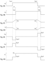
- Figs. 4A-4F illustrate an example of principal wave forms for the gate control signals G 11 and G 12 at turn-on and turn-off off for upper switches S 11 and S 12 of both half-bridges, together with corresponding current and voltage wave forms of Io 1 , Io 2 , U L1 and U L2 .
- An example of a principal wave form of the output voltage U o of the inverter system, referred to N potential is also shown in Fig. 4G .
- the gate signal G 11 causes the upper switch S 11 to turn on (N to P commutation) at a turn-on instant t onS11 and to turn off (P to N commutation) at turn-off instant t offs11 .
- N to P commutation the gate signal
- the gate signal G 12 causes the upper switch S 12 to turn on (N to P commutation) at a turn-on instant t onS12 and to turn off (P to N commutation) at turn-off instant t offS12 .
- a differential current increment ⁇ I d will be induced into the circuit, as illustrated in Figs. 4C and 4D .
- the increment ⁇ I d is the change of the differential current I d during the commutation.
- the differential current increment ⁇ I d is directly proportional to the timing difference ⁇ t .
- the sign of ⁇ I d in the parallel-connected inverter leg INV1 will depend on whether ⁇ I d was during turn-on or turn-off of the switches, and whether S 11 was switching earlier or later than S 12 (i.e., the sign of ⁇ t ) as shown in Table I below.
- the sign of of ⁇ I d in the parallel-connected inverter leg INV2 for S 12 is shown in Table II below.
- the switch S 11 is early to turn on and early to turn off relative to the switch S 12 .
- the leg output current I o1 increases by ⁇ I d ( ⁇ I d > 0) at turn-on of S 11 and decreases by ⁇ I d ( ⁇ I d ⁇ 0) at turn-off of S 11 ( Fig. 4C ).
- the leg output current I 2 decreases by ⁇ I d ( ⁇ I d ⁇ 0) at turn-on of S 12 and increases by ⁇ I d ( ⁇ I d > 0) at turn-off of S 12 ( Fig. 4D ).
- timing difference ⁇ t is drawn to be as long both in turn-on and turn-off in Figs. 4A-4G so that in this example the differential current changes cancel each other out. If the timing differences ⁇ t at turn-on and turn-off were not equal in durations, the changes would not cancel each other.
- each parallel-connected inverter leg (INV1, INV2, ..., INVn), preferably the corresponding switching control (8 1 , 8 2 , ..., 8 n ) thereof, is arranged to sense or measure its leg output current ( I o1 , I o2 ,..., I 0n ) before (step 62 in Fig. 5 ) and after (step 64) the commutation (step 63) to obtain a pre-commutation output current sample ( I o1(pre) , I o2(pre) , ..., I on(pre) and a post-commutation output current sample ( I o1(post) , I o2(post) , ..., I on(post) ).
- each parallel-connected inverter leg will indicate the sign of the timing difference ⁇ t in the respective leg, i.e., whether the switching instant of the respective parallel-connected inverter leg is earlier or later relative to a corresponding switching instant of at least one of the other parallel-connected inverter legs.
- each parallel-connected inverter INV1, INV2, ..., INVn can deduce that its own ⁇ t must have been positive (>0) (e.g., its timing has been early) or its ⁇ t must have been negative ( ⁇ 0) (e.g., its timing has been late).
- a duration of the timing difference ⁇ t can be estimated from the difference ⁇ I o1 , ⁇ I o2 , ..., ⁇ I on (step 66 in Fig. 5 ), e.g., using equation (3).
- the duration of the timing difference ⁇ t can be used in determining the amount of adjustment of the turn-off instant t off or turn-on instant t on in the adjustment steps 67 and 68, for example.
- the leg output currents I o1 , I o2 , ..., I on may be measured in various alternative ways obvious for a person skilled in the art, such as using a shunt current measurement or magnetic sensors.
- the pre-commutation current values I o1(pre) , I o2(pre) , ..., I on(pre and the post-commutation current values I o1(post) , I o2(post) , ..., I on(post) can be sampled either in an analogue circuit or a digital circuit.
- An existing current measurement needed for other control purposes in an inverter leg may also be used for the purposes of the present invention, if the filtering and limited sampling rate of the current did not deteriorate the useful signal for the extraction of I o(post) - I o(pre) .
- the inverter leg INV1, INV2, ..., INVn may monitor a voltage U Lo1 , U Lo2 , ..., U Lon (step 74 in Fig. 6 ) which is created across the output inductor L o1 , L 02 , ..., L on during commutation (step 73), if there is a timing difference ⁇ t in the switching.
- a voltage U Lo1 , U Lo2 , ..., U Lon step 74 in Fig. 6
- Lo1 , L 02 , ..., L on during commutation step 73
- positive or negative voltage pulses U Lo1 and U Lo2 will be created across the inductors L o1 and L o2 of the inverter legs INV1 and INV2, respectively, due to a timing difference ⁇ t
- the sign of voltage pulse U Lo1 or U Lo2 in the parallel-connected inverter leg INV1 or INV2 will depend on whether the voltage pulse was during turn-on or turn-off of the switches, and whether the switching in the respective parallel inverter leg earlier ( ⁇ t >0) or later ( ⁇ t ⁇ 0) than the switching in the other parallel-connected inverter leg (i.e., the sign of ⁇ t ).
- the positive and negative differential current increments ⁇ I d in the output currents I o1 and I o2 of the inverter legs INV1 and INV2, respectively, are formed as an integral of the inductor voltage pulses U Lo1 and U Lo2 over the timing difference ⁇ t .
- the switch S 11 is early to turn on and early to turn off relative to the switch S 12 ( ⁇ t >0).
- a negative voltage pulse U Lo1 is created across the inductor L o1 at turn-on of S 11 and a positive voltage pulse U Lo1 is created across the inductor L o1 at turn-off of S 11 ( Fig. 4E ), causing a positive ⁇ I d ( ⁇ I d > 0) at turn-on of S 11 and a negative ⁇ I d ( ⁇ I d ⁇ 0) at turn-off of S 11 .
- a positive voltage pulse U Lo2 is created across the inductor L o2 at turn-off of S 12 and a negative voltage pulse U Lo2 is created across the inductor L o2 at turn-on of S 12 ( Fig. 4F ), causing a negative ⁇ I d ( ⁇ I d ⁇ 0) at turn-off of S 12 and a positive ⁇ I d ( ⁇ I d > 0) at turn-on of S 12 .
- each parallel-connected inverter INV1, INV2, ..., INVn can deduce that its own ⁇ t must have been positive (>0) (e.g., its timing has been early) or its ⁇ t must have been negative ( ⁇ 0) (e.g., its timing has been late).
- Each parallel-connected inverter leg INV1, INV2, ..., INVn can now make an adjustment to its turn-off instant t off or turn-on instant t on in such way that the adjustment either increases ⁇ I d ( ⁇ t ) from negative towards zero (step 77) or decreases ⁇ I d ( ⁇ t ) from positive towards zero (step 78). If the voltage U Lo1 , U Lo2 , ..., U Lon (or ⁇ t ) is approximately zero, no timing adjustment may be needed (step79).
- the monitoring, analysis and adjustment is preferably carried out for each commutation event, i.e., every turn-on or turn-off of the switch (every N to P or P to N commutation).
- the adjusted t off or t on can be used in a subsequent (in the next, for example) turn-off or turn-on of the switch.
- the adjustments may be stored and further adjusted in the subsequent commutations, e.g., using an integral action controller.
- sensing, analysis and adjustment may not be carried out for each commutation event as in an optimal adjustment but for a selective portion all commutations, such as for sequentially selected commutations, for certain commutations only, or for alternating commutations.
- the duration of the timing difference ⁇ t can also be acquired directly from the width or duration of the voltage pulse U Lo1 , U Lo2 , ..., U Lon . Therefore, a benefit of voltage measurement-based approach may be the speed and simplicity of measurement, as there is no need for a current sampling and indirect estimation of ⁇ t from the ⁇ I o by means of equation (3), for example.
- the duration of the timing difference ⁇ t can be used in determining the amount of adjustment of the turn-off instant t off or turn-on instant t on in the adjustment steps 77 and 78, for example.
- the voltage U Lo1 , U Lo2 , ..., U Lon may be integrated by an integrator circuit during the commutation to acquire a measure of ⁇ I d .
- the measure of ⁇ I d can be used in determining the amount of adjustment of the turn-off instant t off or turn-on instant t on in the adjustment steps 77 and 78, for example.
- the determination of the duration or width of the voltage pulse across the output inductor, and/or the integration of the voltage pulse across the output inductor can be implemented in an analogue or digital circuit.
- the voltage measurement-based approach could possibly be made faster and real-time with analogue electronics.
- the timing adjustment may comprise postponing the turn-off instant t off or the turn-on instant t on of the respective switch to decrease the current increment ⁇ I d and/or the timing difference ⁇ t towards zero, if the switch is switching early ( ⁇ t > 0), and advancing the turn-off instant t off or the turn-on instant t on of the respective switch to increase the current increment ⁇ I d and/or the timing difference ⁇ t towards zero, if the switch is switching early ( ⁇ t ⁇ 0).
- the timing difference ⁇ t and/or the current increments ⁇ I d in individual commutations are controlled by adjusting the switching instants so that the timing difference ⁇ t and/or the current increment ⁇ I d is not zero during commutations but stays bounded while an output voltage of the inverter system will swing in a stepwise manner.
- the timing difference ⁇ t and/or the current increments ⁇ I d in individual commutations are controlled to a fixed non-zero value by adjusting the switching instants, the fixed non-zero value being equal in a turn-on commutation and a turn-off commutation.
- the differential current I d jumps back and forth by ⁇ I d but stays bounded.
- An example of a resulting behavior of the output voltage U o of the inverter system is illustrated in in Fig. 4G : the swings of the output voltage U o from N to P and from P to N occur in a step wise manner.
- the stepwise swing of the output voltage may be beneficial in some applications. In motor drive applications, a stepwise output voltage fed to a motor winding, for example, would ease the stress on motor insulation and bearings.
- the amount of adjustment of the turn-off instant t off or the turn-on instant t on of the respective switch may be approximately half of the duration of the timing difference ⁇ t . Because the adjustment is made to opposite directions in the two parallel-connected inverter legs, the total amount of adjustments will be approximately ⁇ t , thereby cancelling the timing difference or the current difference between the two legs in subsequent commutations.
- the switching control and timing adjustment techniques described herein may be implemented by various means. For example, these techniques may be implemented in hardware (one or more analog or digital and/devices), firmware (one or more devices), software (one or more modules), or combinations thereof. For a firmware or software, implementation can be through modules (e.g., procedures, functions, and so on) that perform the functions described herein.
- the software codes may be stored in any suitable, processor/computer-readable data storage medium(s) or memory unit(s) and executed by one or more processors/computers.
- the data storage medium or the memory unit may be implemented within the processor/computer or external to the processor/computer, in which case it can be communicatively coupled to the processor/computer via various means as is known in the art.
- components of systems described herein may be rearranged and/or complimented by additional components in order to facilitate achieving the various aspects, goals, advantages, etc., described with regard thereto, and are not limited to the precise configurations set forth in a given figure, as will be appreciated by one skilled in the art.
Landscapes
- Engineering & Computer Science (AREA)
- Power Engineering (AREA)
- Inverter Devices (AREA)
Abstract

Description
- The present invention relates to parallel-connected power inverters, and more particularly to a current sharing of parallel-connected power inverters.
- A dc-ac converter, also known as an inverter, converts dc power to ac power at desired output voltage and output frequency. The inverter therefore can be operated as an adjustable-frequency voltage source. The dc power input to the inverter may be obtained from an existing power supply network through a rectifier or from a battery, fuel cell, photovoltaic array, etc. The filter capacitor(s) across the input terminals of the inverter provides a fairly constant dc-link voltage. A configuration of ac to dc converter and dc to ac inverter may be called a dc-link converter.
- In some situations, a power inverter with an increased output power capability is implemented by connecting a plurality of inverter units in parallel with one another to feed the same load through output reactors. The parallel-connected inverter units may receive simultaneous and similar control signals to provide a desired output of the power inverter. However, due to parameter differences of switch components and differing impedances in parallel branches, the currents between the units can be unequal in magnitude. Such a current imbalance can stress the components unevenly and wear switch components with higher current prematurely. A higher current in a switch component can result in a higher dissipated power and, further, a higher temperature of the component.
- Current imbalance has been addressed by modifying switch control pulses in order to balance the currents. The control pulses can be modified by delaying a turn-on time instant for a switch that has the highest current or by delaying turn-off time instants for a switch that has the smallest current. One such method is disclosed in
EP0524398 . In these solutions, the conducting times of the parallel components are modified to equalize stresses to the switch components on the basis of measured inverter unit currents. -
US8432714 discloses a method for balancing load between parallel-connected inverters wherein temperatures of each output leg of each inverter are determined and the switching instructions for one or more of the parallel inverters are modified for controlling the temperatures of the output legs. -
WO2017079125A1 discloses a method wherein the output voltages of all the parallel connected power devices are measured, and the measuring results are used for mitigating timing differences during output voltage state changes caused e.g. by gate driver circuit and switching component parameter tolerances. -
US7068525 discloses a method of operating multiple parallel-connected inverters by regulating the individual currents of the inverters separately. - An object of the present invention is to provide an improved power inverter system having two or more parallel-connected inverter legs. The power inverter system is recited in the
independent claim 1. Preferred embodiments are disclosed in the dependent claims. - An aspect of the invention is a power inverter system, comprising
- two or more switching mode inverter legs connected in parallel between a common DC input and a common phase output to feed a phase output current to a common load, the phase output current being formed by combined leg output currents of the parallel-connected inverter legs, wherein commutations of the parallel-connected inverter legs are initiated by essentially simultaneous commutation commands,
- a control arrangement configured to balance current sharing between the parallel-connected inverter legs by means of adjusting switching instants of main switches of the parallel-connected inverter legs,
- wherein the control arrangement is configured to sense the leg output current before and after a commutation in each of the parallel-connected inverter legs to obtain a pre-commutation current value and a post-commutation current value, and wherein the control arrangement is configured to adjust switching instants of the main switches for subsequent commutation autonomously in each of the parallel-connected inverter legs based on a difference between the pre-commutation and the post-commutation current values of the respective parallel-connected inverter leg to control the difference towards zero, the difference being representative of a timing difference between switching instants of the respective parallel-connected inverter leg and at least one of the other parallel-connected inverter legs.
- In an embodiment, if a sign of the difference between the pre-commutation and the post-commutation current values is negative, the control arrangement is configured to adjust switching instants for subsequent commutation so as to increase the negative difference towards zero, and wherein, if a sign of the difference between the pre-commutation and the post-commutation current values is positive, the control arrangement is configured to adjust switching instants for subsequent commutation so as to decrease the positive difference towards zero.
- In an embodiment, the sign of the difference between the pre-commutation and the post-commutation current values indicates whether the switching instant of the parallel-connected inverter leg is earlier or later relative to a corresponding switching instant of at least one of the other parallel-connected inverter legs, and wherein the control arrangement is configured to advance the switching instants of the main switch, if the sign of the difference between the pre-commutation and the post-commutation current values indicates the switching instant of the parallel-connected inverter leg is later relative to a corresponding switching instants of at least one other parallel-connected inverter leg.
- An another aspect of the invention is a power inverter system, comprising
- two or more switching mode inverter legs connected in parallel between a common DC input and, via leg output inductors, a common phase output to feed a phase output current to a common load, the phase output current being formed by combined leg output currents of the parallel-connected inverter legs, wherein commutations of the parallel-connected inverter legs are initiated by essentially simultaneous commutation commands,
- a control arrangement configured to balance current sharing between the parallel-connected inverter legs by means of adjusting switching instants of main switches of the parallel-connected inverter legs,
- wherein the control arrangement is configured to sense a voltage pulse over the leg output inductor in each of the parallel-connected inverter legs during the commutation, and wherein the control arrangement is configured to adjust the switching instants autonomously in each of the parallel-connected inverter legs based on the duration and/or sign of the sensed output inductor voltage pulse or an integral of the voltage pulse of the respective parallel-connected inverter leg to control the magnitude and direction of a commutation-induced current difference towards zero.
- In an embodiment, the integral of the sensed voltage pulse represents a magnitude of the commutation-induced current difference in the parallel-connected inverter leg.
- In an embodiment, the duration of the sensed voltage pulse represents a timing difference of a switching instant of the parallel-connected inverter leg relative to a corresponding switching instant of at least one other parallel-connected inverter leg.
- In an embodiment, the sign of the sensed voltage pulse indicates whether the switching instant of the parallel-connected inverter leg is earlier or later relative to a corresponding switching instant of at least one other parallel-connected inverter leg.
- In an embodiment, the control arrangement is configured to advance the switching instant of the parallel-connected inverter leg, if the sign of the voltage pulse indicates the switching instant of the parallel-connected inverter leg is later relative to a corresponding switching instant of at least one other parallel-connected inverter leg; and wherein the control arrangement is configured to delay the switching instant of the parallel-connected inverter leg, if the sign of the voltage pulse indicates the switching instant of the parallel-connected inverter leg is earlier relative to a corresponding switching instant of at least one other parallel-connected inverter leg.
- In an embodiment, the control arrangement is configured to carry out the sensing and adjustment of the switching instants during all commutations or during a selected portion of the commutations.
- In an embodiment, the control arrangement is configured to carry out the sensing at each turn-on and turn-off of the main switches.
- In an embodiment, the control arrangement is configured to adjust the switching instants of the main switches to control the commutation-induced current difference or a timing difference in an individual commutation towards zero but not to zero thereby causing a stepwise swing of a phase output voltage of the inverter system during an individual commutation.
- In an embodiment, the control arrangement is configured to adjust the switching instant of the main switches to control the commutation-induced current difference or a timing difference in an individual commutation towards zero to a predetermined non-zero value that is equal for turn-on and turn-off of the main switches, thereby causing a stepwise swing of a phase output voltage of the inverter system during an individual commutation.
- In an embodiment, the control arrangement comprises a leg-specific controller for each of the two or more parallel-connected inverter legs to adjust the switching instants of the main switches.
- In an embodiment, the power inverter system comprises two or more inverters, each of the inverters comprising one or more inverter phase legs, wherein the parallel-connected inverter legs are the corresponding inverter phase legs of the two or more inverters modules connected in parallel.
- In an embodiment, the control arrangement comprises inverter-specific switching controllers for the two or more inverters, each of the inverter-specific switching controllers being configured to provide the autonomous adjustment of switching instants for each of the inverter phase legs of the respective inverter.
- In the following the invention will be described in greater detail by means of exemplary embodiments with reference to the accompanying drawings, in which
-
Figure 1 is a block diagram that schematically illustrates an exemplary inverter system having a plurality of parallel-connected inverters; -
Figure 2 is a schematic of an exemplary inverter system having two parallel-connected inverters; -
Figure 3 is a schematic block diagram of an exemplary embodiment of a switching controller; -
Figures 4A-4G illustrate an example of principal waveforms for the gate control signals at turn-on and turn-off off for upper switches and for corresponding leg output currents, voltages across output inductors and an inverter output voltage of two parallel-connected inverter legs ofFig. 2 ; -
Figure 5 is a flow diagram illustrating an exemplary procedure for an autonomous switching timing adjustment of parallel-connected inverter legs based on measuring output current before and after the commutation; and -
Figure 6 is a flow diagram illustrating an exemplary procedure for an autonomous switching timing adjustment of parallel-connected inverter legs based on measuring a voltage across an output inductor during the commutation. -
Fig. 1 shows a block diagram that schematically illustrates an exemplary inverter system having a plurality of (i.e., two or more) inverters INV1, INV2, ..., INVN connected in parallel from their DC side (e.g., DC link) input terminals (e.g., dc+, dc-) and their AC side output terminals (e.g., U1, V1, W1, Uz, V2, W2). In the illustrated example, the inverters INV1 and INV2 are three-phase inverters providing three phase outputs U1, V1, W1 and U2, V2, W2, but it should be appreciated that parallel-connected inverters may be implemented as single-phase inverters, or generally include any number of inverter phases or phase legs. The parallel-connected inverters are fed by a commonDC voltage source 4 with voltage Udc, and inverters are feeding acommon AC load 6. A typical application area of the parallel-connected inverters fed by a commonDC voltage source 4 is an electric motor drive having an AC electric motor as acommon load 6. It should be noted that theload 6 does not have to be of AC type. It can be DC as well, for example a battery energy storage or similar. Parallel connected inverter phase legs apply this invention similarly, regardless of the load type. There is a non-zero impedance at each phase output of the inverters, represented by inductances Lo inFig. 1 . The output inductances Lo may be intentionally implemented (e.g., an inductor, a coil, a choke, etc.) or it may be just some leakage impedance of practical components and materials, such as cabling. The output inductances Lo may be substantially equal, but it must not necessarily be so. The corresponding phase outputs U1, U2, V1, V2, and W1, W2 of the parallel-connected inverters INV1 and INV2 are connected through the output inductances Lo to the common phase outputs U, V, and W, respectively. The corresponding phase outputs U1, U2, V1, V2, and W1, W2 of the parallel-connected inverters INV1 and INV2 may be connected together right after the output inductances Lo, and a single cable or multiple cables per phase U, V, and W may be used to connect the phase outputs to theload 6. Alternatively, each parallel-connected inverter INV1 and INV2 can be connected by means of its own cabling to theload 6, and the phase outputs U1, U2, V1, V2, and W1, W2 can be connected in parallel first at the terminals of theload 6. Output phase current Io of each phase U, V, W supplied to theload 6 is formed by combining phase output currents Io1 and Io2 of the respective phase outputs U1, U2, V1, V2, and W1, W2 of the parallel-connected inverters INV1 and INV2. The common DC supplied parallel-connected inverters INV1 and INV2 can be controlled to act like one high power inverter. This can be achieved by controlling the parallel inverters with essentially same control commands. - Each inverter INV1 and INV2 may have one or more half bridge legs, which can be functionally independent of each other or parallel connected inside an inverter (INV1 or INV2). The functionally similar bridge legs of the same phase of different inverters (INV1 and INV2) are connected in parallel with one another. Each bridge circuit can include a plurality of electronic switching elements or devices (e.g. insulated gate bipolar transistors (IGBTs)) that operate in a switch mode, meaning that that they are controlled to transition from a blocking state (OFF state) to a conducting state (ON state), and vice-versa, by providing control pulses (often called switching control signals or gating signals) at a high switching frequency. In a PWM modulation scheme, the width of control pulses provided to the control inputs of the switching devices is varied to provide a desired output of the inverter. The parallel-connected inverters INV1 and INV2 may have a common switching control (e.g., as a part of the
higher level control 86 inFig. 1 ) that provides switching signals or gating signals to operate switching devices of all inverters, or each parallel-connected inverter INV1 and INV2 may have a dedicatedswitching control unit Fig. 1 . Alternatively, the control may be distributed among a common switching control unit and inverter-specific switching control units. In the latter cases, the inverters may be normal inverters (i.e., that can be used as single units) that can be connected in parallel as such. In embodiments, the switching control(s) 81 and 82 of the parallel-connected inverters INV1 and INV2 may be controlled by a higher-level control system 86 with simultaneous and essentially similar control signals or commands. - In embodiments, the higher-
level control system 86 may be an electric motor control system or similar. It can also include a common PWM generation function (for example, a PWM modulator) for all system elements and phases. - The schematic of an exemplary inverter system (e.g., single-phase inverter system) having two inverters INV1 and INV2 connected in parallel is illustrated in
Figure 2 and described herein in order to alleviate comprehending operation and configuration of embodiments of the invention in relation to exemplary basic parallel-connected inverters. It is not intended to limit embodiments of the invention to the described and illustrated exemplary inverters. It shall be appreciated that the current sharing control according to embodiments of the invention is universally applicable to any number of parallel inverters, any type of inverters and their derivates and modifications regardless the specific design, configuration, and operation variations of an inverter from the exemplary inverter. - The parallel-connected inverters INV1 and INV2 may preferably be identical inverters having the same configuration and operation. The inverters INV1 and INV2 comprise
power switching sections 10, such as half-bridge circuits, and dc-link rails 22 (positive dc-link potentials P) are connected to a first voltage terminal Udc+ of the commonDC power source 4, and dc-link rails 24 (negative dc-link potentials N) are connected to a second voltage terminal Udc- of the commonDC power source 4. Theoutput node 110 of eachpower switching section 10 can be connected through the corresponding output inductance Lo1 and Lo2 to the corresponding phase terminal of anac load 6, such as an ac motor or ac grid or any applicable electric load. and thereby thecorresponding phase outputs 110 of the inverters INV1 and INV2 (e.g., phase legs U1 and U2) are connected in parallel via Lo1 and Lo2. It should be appreciated that although a half-bridge inverter is illustrated as an example herein, the inverter may have other configurations, particularly a full-bridge configuration. - The common dc power input to the parallel-connected inverters INV1 and INV2 may be obtained from any kind of a
dc power source 4, such as from an existing power supply network through a rectifier, or from a battery, fuel cell, photovoltaic array, etc. It shall be appreciated that dc-link 2 may be provided in several forms and may have a number of voltages and other attributes. It shall also be appreciated that the voltage difference between positive and negative dc-link rails is flexible, depending on how the dc-link 2 is fed. It shall be further appreciated the term bus may be utilized in place of the term link such that, for example, references to a dc-link are understood to encompass a dc-bus and vice versa. - It should be appreciated that although a single-phase inverter is illustrated as an example herein, an inverter may be implemented as a three-phase inverter, or generally include any number of inverter phases or phase legs. For example, inverters INV1 and INV2 illustrated in
Figure 2 may be implemented as three-phase inverters including a power section 10u, 10v and 10w for each phase or phase leg U1, U2, V1, V2, W1 and W2, respectively. Operation and configuration of the other phases or phase legs V1, V2, W1 and W2 of the inverters INV1 and INV2 can be identical to the operation and configuration described for the phases or phase legs U1 and U2 above. - In embodiments, three-phase inverters INV1 and INV2 may each comprise a dc-link with dc-link capacitors (e.g., a dc-link illustrated in
Fig. 3 ) common to all thepower sections - In embodiments, all
power sections specific switching controller 81. Similarly, in embodiments, all power sections 10u, 10v and 10w of phase legs U2, V2 and W2 in the inverter INV2 may be controlled by the same inverter-specific switching controller 8z. -
Fig. 3 is a schematic block diagram of an exemplary embodiment of a switchingcontroller switching control function 84 that includes a dedicatedswitching control module 841A, 841B, and 841C adapted to provide control signals, such as G1, G2, ..., Gn to each phase leg U1, V1 and W1, respectively, based on a respective PWM signal PWMu, PWMv and PWMw received from a PWM modulator. The PWM modulator may be common for all parallel-connected inverters INV1...INVn (e.g., as a part of the higher-level control 86 inFig. 1 , and the PWM commands may be sent via a communication link to the inverters. In embodiments, a leg-specific output current sensing and/or a leg-specific inductor voltage sensing feedback FD may be provided for each leg-specificswitching control module 841A, 841B, and 841C. In embodiments, a leg-specific current balancing may be included in the switchingcontrol 84, and particularly in the leg-specificswitching control modules 841A, 841B, and 841C. In embodiments, a leg-specific current balancing may be implemented by means of Field Programmable Gate Arrays (FPGAs). - Referring again to
Fig. 2 , the exemplary half-bridge power section 10 of the inverter INV1 illustrated inFig. 2 includes a pair of main or power switching devices S11 and S21 coupled in parallel to the dc-link rails link rail 22 and a second terminal electrically coupled to anoutput node 110. The second (lower) main switching device S21 having a first terminal coupled tooutput node 110 and a second terminal coupled to the negative dc-link rail 24. Across the upper main switching device S11 between the positive dc-link rail 22 and theoutput node 110 is connected a first antiparallel diode D11, and across the lower main switching device S21 between theoutput node 110 and the negative dc-link rail 24 is connected a second antiparallel diode D21. The upper main switching device S21 is operable to turn on and turn off, and thereby to respectively connect and disconnect the dc-link rail 22 and theoutput node 110, in response to control signal(s) G11 received from a control and driver circuitry, such as an inverter-specific switching controller 81 illustrated inFig. 2 . The lower main switching device S21 is operable to turn on and turn off, and thereby to respectively connect and disconnect the dc-link rail 24 and theoutput node 110, in response to control signal(s) G21 received from the control and driver circuitry, such as the switchingcontroller 81. Similarly, the exemplary half-bridge power section 10A of the inverter INV2 illustrated inFig. 2 includes a pair of main or power switching devices S12 and S22, a first antiparallel diode D12, a second antiparallel diode D22, and switching control signals G12 and G22 from a control and driver circuitry, such as an inverter-specific switching controller 82. In embodiments, the switching devices S11, S12, S21 and S22 may be insulated gate bipolar transistors (IGBT), or other type of semiconductor switching devices, such as integrated gate-commutated thyristors (IGCT), metal-oxide-semiconductor field-effect transistors (MOSFET), or silicon carbide (SiC) MOSFETs to name several examples. - In operation, when the output current Io is positive (Io1 > 0, Io2 > 0) and the upper main switch S11/S12 is turned on (to a conductive state), a first switch current Is11/ Is12 can flow between the dc-
link rail 22 and theoutput node 110. Similarly, when the output current Io is negative (Io1 < 0, Io2 < 0) and the lower main switching device S21/S22 is turned on (to a conductive state), a second switch current Is21/ Is22 can flow between theoutput node 110 and the dc-link rail 24. On the other hand, when the upper switching device S11/S12 is turned off (to a non-conductive state), the first switch current Is11/Is12 will not flow in the switch-forward direction between the dc-link rail 22 and theoutput node 110, although a current Id11/Id12 may flow in the switch-reverse direction through the first anti-parallel diode D11/D12 of the upper main switching device S11/S12,, if the output current Io is negative (Io1 < 0, Io2 < 0). Similarly, when the lower main switching device S21/S22 is turned off (to a non-conductive state), the second switch current Is21/Is22 will not flow in the switch-forward direction between theoutput node 110 and the dc-link rail 24, although a current Id21/Id22 may flow in the switch-reverse direction through the anti-parallel diode D21/D22 of the lower switching device S21/S22, if the output current Io is positive (Io1 > 0, Io2 > 0). Thus, by turning on and off and closing the upper main switching device S11/S12 and the lower main switching device S21/S22, the output voltage at theoutput node 110 will be controlled or commutated to be either the potential P from the dc-link rail 22 or the potential N from the dc-link rail 24. - More specifically, when the output current Io is positive (Io1 > 0, Io2 > 0), it is the upper switches S11 and S12 that commutate their currents (Is11 and Is12, respectively) to diodes D21 and D22, respectively, and the output voltage Uo swings from the potential P (the dc-link 22) to the potential N (the dc-link 24). When the output current Io is negative (Io1 < 0, Io2 < 0), it is the lower switches S21 and S22 that commutate their currents (Is21 and Is22, respectively) to diodes D11 and D12, respectively, and the output voltage Uo swings from the potential N (the dc-link 24) to the potential P (the dc-link 22).
- The commutation for a corresponding phase in the plurality of parallel-connected inverters, e.g., for the phase U1 of the inverter INV1 and the phase U2 of the inverter INV2, can be initiated by similar commutation commands at the same time instant. In an ideal case, the output currents Io1 and Io2 of the parallel-connected inverters would be equal and their difference or a differential output current Ido would be zero, (e.g., Ido = Io1 - Io2 = 0). However, the ideal behavior during commutations would require that the corresponding switches, e.g., upper switches S11 and S12, in the parallel operated inverters turn on at the same instant when commutating the output potential Uo, for example from N to P. Likewise, the corresponding switches, e.g., upper switches S11 and S12, in the parallel operated inverters should turn off at the same instant when commutating the output potential, for example from P to N. Unfortunately, the parallel operated inverters do not behave similarly, for example due to parameter differences of switch components and differing impedances in parallel branches, the output currents from the parallel inverters can be unequal in magnitude, and a current difference, here defined as I do = I o1 - I o2 ≠ 0, will evolve. In other words, there can be uneven current sharing between the inverters. Due to thermal and economic reasons, it is of utmost importance that the parallel-connected inverters share the load current as evenly as possible.
- According to an aspect of the invention, a current sharing between the parallel-connected inverter legs is balanced by means of adjusting switching instants of main switches of the parallel-connected inverter legs, by a control arrangement, such as the switching controls
functions 84 or switching control module 841u, 841v, and 841w. The control arrangement may sense the leg output current before and after a commutation in each of the parallel-connected inverter legs to obtain a pre-commutation current value and a post-commutation current value, and the control arrangement may adjust switching instants of the main switches for next commutation autonomously in each of the parallel-connected inverter legs based on a difference between the pre-commutation and the post-commutation current values of the respective parallel-connected inverter leg to control the difference towards zero, the difference being representative of a timing difference and/or a commutation-induced current difference between the respective parallel-connected inverter leg and at least one of the other parallel-connected inverter legs. Thereby, the control arrangement can balance the current sharing by fine tuning the switching instants which may otherwise be generated in a conventional manner. - Let us examine the situation for a case where the output current Io is positive (Io1 > 0, Io2 > 0) in the exemplary inverter system shown in
Fig. 2 , i.e., the upper switches S11 and S12 commutate their currents (Is11 and Is12, respectively) to diodes D21 and D22, respectively. -
Figs. 4A-4F illustrate an example of principal wave forms for the gate control signals G11 and G12 at turn-on and turn-off off for upper switches S11 and S12 of both half-bridges, together with corresponding current and voltage wave forms of Io 1 , Io 2, U L1 and U L2. An example of a principal wave form of the output voltage Uo of the inverter system, referred to N potential is also shown inFig. 4G . InFig. 4A , the gate signal G11 causes the upper switch S11 to turn on (N to P commutation) at a turn-on instant t onS11 and to turn off (P to N commutation) at turn-off instant t offs11. Similarly, inFig. 4B , the gate signal G12 causes the upper switch S12 to turn on (N to P commutation) at a turn-on instant t onS12 and to turn off (P to N commutation) at turn-off instant t offS12. - Let us also define the timing difference Δt of the parallel-connected inverter legs for turn-on and turn-off as


- t onS11 is a turn-on instant of S11
- t onS12 is a turn-on instant of S12
- t offS11 is a turn-off instant of S11
- t offS12 is a turn-off instant of S12.
- If there is a difference of magnitude Δt in either the turn-on instants or the turn-off instants of the upper switches S 11 and S 12, a differential current increment ΔI d will be induced into the circuit, as illustrated in
Figs. 4C and 4D . The increment ΔI d is the change of the differential current Id during the commutation. The magnitude of the increment will be
- At is Δton or Δtoff
- Udc is the dc link voltage (known or measured)
- Lo1 and Lo2 are output inductances.
- It can be seen in equation (3) that the differential current increment ΔI d is directly proportional to the timing difference Δt. The sign of ΔI d in the parallel-connected inverter leg INV1 will depend on whether ΔI d was during turn-on or turn-off of the switches, and whether S11 was switching earlier or later than S 12 (i.e., the sign of Δt) as shown in Table I below. Similarly, the sign of of ΔI d in the parallel-connected inverter leg INV2 for S12 is shown in Table II below. It can be seen that the sign of ΔI d and the sign of Δt in one of the parallel-connected inverter legs INV1 and INV2 are opposite to those in the other one of the parallel-connected inverter legs INV1 and INV2. The Tables I and II represent the same situation but from perspective of different inverter INV1 and INV2, respectively. The top row of Table I and bottom row of Table II describe the same situation and they have opposite polarity for the differential current increment ΔI d. Same applies for bottom row of Table I and top row of Table II. Similar tables can be readily provided for a case where the output current Io is negative (Io1 < 0, Io2 < 0) in the exemplary inverter system shown in
Fig. 2 , i.e., the lower switches S21 and S22 commutate their currents (Is21 and Is22, respectively) to upper diodes D11 and D12, respectively.Table I INV1 Turn-on (Uo from N to P) Turn-off (Uo from P to N) S11 turns on or off before S12 (Δton > 0 or Δtoff > 0) ΔI d > 0 ΔI d < 0 S11 turns on or off after S12 (Δton < 0 or Δtoff < 0) ΔI d < 0 ΔI d > 0 Table II INV2 Turn-on (Uo from N to P) Turn-off (Uo from P to N) S 12 turns on or off before S 11 (Δton > 0 or Δtoff > 0) ΔI d > 0 ΔI d < 0 S 12 turns on or off after S 11 (Δton < 0 or Δtoff < 0) ΔI d < 0 ΔI d > 0 - In the example shown in
Figs. 4A-4G , the switch S 11 is early to turn on and early to turn off relative to the switch S12. Thus, in the leg INV1, the leg output current I o1 increases by ΔI d (ΔI d > 0) at turn-on of S11 and decreases by ΔI d (ΔI d < 0) at turn-off of S11 (Fig. 4C ). In the leg INV2, the leg output current I 2 decreases by ΔI d (ΔI d < 0) at turn-on of S12 and increases by ΔI d (ΔI d > 0) at turn-off of S12 (Fig. 4D ). For simplicity, the timing difference Δt is drawn to be as long both in turn-on and turn-off inFigs. 4A-4G so that in this example the differential current changes cancel each other out. If the timing differences Δt at turn-on and turn-off were not equal in durations, the changes would not cancel each other. - In embodiments, each parallel-connected inverter leg (INV1, INV2, ..., INVn), preferably the corresponding switching control (81, 82, ..., 8n) thereof, is arranged to sense or measure its leg output current (I o1, Io2 ,..., I0n) before (
step 62 inFig. 5 ) and after (step 64) the commutation (step 63) to obtain a pre-commutation output current sample ( I o1(pre) , I o2(pre) , ..., I on(pre) and a post-commutation output current sample ( I o1(post) , I o2(post) , ..., I on(post)). This way each parallel-connected inverter leg (INV1, INV2, ..., INVn), preferably the switching control (81, 82, ..., INVn) thereof, can acquire the increment ΔI d as differences ΔI o1 = I o1(post) - I o1(pre), ΔI o2 = I o2(post) - I o2(pre), ... , ΔI on = I on(post) - I on(pre), respectively (step 65). The sign of the difference ΔI o1, ΔI o2, ..., ΔI on in each parallel-connected inverter leg will indicate the sign of the timing difference Δt in the respective leg, i.e., whether the switching instant of the respective parallel-connected inverter leg is earlier or later relative to a corresponding switching instant of at least one of the other parallel-connected inverter legs. - Further, the differences ΔI o1, ΔI o2 , ..., ΔI on will be of opposite sign in the parallel-connected inverters having a timing difference, as illustrated in Tables I and II. Hence, based on the sign of the difference ΔI o1, ΔI o2 , ..., ΔI on (or the sign of Δt) in the respective parallel-connected leg (step 66), each parallel-connected inverter INV1, INV2, ..., INVn can deduce that its own Δt must have been positive (>0) (e.g., its timing has been early) or its Δt must have been negative (<0) (e.g., its timing has been late). Each parallel-connected inverter leg INV1, INV2, ..., INVn can now make an adjustment to its turn-off instant t off or turn-on instant t on in such way that the adjustment either increases ΔI d (Δt) from negative towards zero (step 67) or decreases ΔI d (Δt) from positive towards zero (step 68). If the difference ΔI o (or Δt) is approximately zero, no timing adjustment may be needed (step 69). The sensing, analysis and adjustment is preferably carried out for each commutation event, i.e., every turn-on or turn-off of the switch (every N to P or P to N commutation). The adjusted t off or t on can be used in in a subsequent (in the next, for example) turn-off or turn-on of the switch. In embodiments, the adjustments may be stored and further adjusted in the subsequent commutations, e.g., using an integral action controller. In embodiments, if a less optimal adjustment is satisfactory, sensing, analysis and adjustment may not be carried out for each commutation event as in an optimal adjustment but for a selective portion all commutations, such as for sequentially selected commutations, for certain commutations only, or for alternating commutations.
- In embodiments, also a duration of the timing difference Δt can be estimated from the difference ΔI o1, ΔI o2 , ..., ΔI on (
step 66 inFig. 5 ), e.g., using equation (3). The duration of the timing difference Δt can be used in determining the amount of adjustment of the turn-off instant t off or turn-on instant t on in the adjustment steps 67 and 68, for example. - The leg output currents I o1, I o2, ..., I on may be measured in various alternative ways obvious for a person skilled in the art, such as using a shunt current measurement or magnetic sensors. The pre-commutation current values I o1(pre) , I o2(pre) , ..., I on(pre and the post-commutation current values I o1(post) , I o2(post) , ..., I on(post) can be sampled either in an analogue circuit or a digital circuit. An existing current measurement needed for other control purposes in an inverter leg may also be used for the purposes of the present invention, if the filtering and limited sampling rate of the current did not deteriorate the useful signal for the extraction of I o(post) - I o(pre).
- According to an aspect of the invention, a control arrangement, such as the switching controls
functions 84 or switching control module 841u, 841v, and 841w, is configured to sense a voltage pulse over the leg output inductor in each of the parallel-connected inverter legs during the commutation, and the control arrangement is configured to adjust the switching instants autonomously in each of the parallel-connected inverter legs based on the duration and/or sign of the sensed output inductor voltage pulse or an integral of the voltage pulse of the respective parallel-connected inverter leg to control the magnitude and direction of a commutation-induced current difference towards zero. Thereby, the control arrangement can balance the current sharing by fine tuning the switching instants which may otherwise be generated in a conventional manner. - Referring to the exemplary inverter system shown in
Fig. 2 , the inverter leg INV1, INV2, ..., INVn may monitor a voltage U Lo1, U Lo2, ..., U Lon (step 74 inFig. 6 ) which is created across the output inductor L o1, L 02, ..., Lon during commutation (step 73), if there is a timing difference Δt in the switching. As can be seen inFigs. 4E and 4F , positive or negative voltage pulses ULo1 and ULo2 will be created across the inductors Lo1 and Lo2 of the inverter legs INV1 and INV2, respectively, due to a timing difference Δt The sign of voltage pulse ULo1 or ULo2 in the parallel-connected inverter leg INV1 or INV2 will depend on whether the voltage pulse was during turn-on or turn-off of the switches, and whether the switching in the respective parallel inverter leg earlier (Δt >0) or later (Δt < 0) than the switching in the other parallel-connected inverter leg (i.e., the sign of Δt). Finally, the positive and negative differential current increments ΔI d in the output currents Io1 and Io2 of the inverter legs INV1 and INV2, respectively, are formed as an integral of the inductor voltage pulses ULo1 and ULo2 over the timing difference Δt. - In the example shown in
Figs. 4A-4G , the switch S 11 is early to turn on and early to turn off relative to the switch S12 (Δt >0). Thus, in the leg INV1, a negative voltage pulse ULo1 is created across the inductor Lo1 at turn-on of S11 and a positive voltage pulse ULo1 is created across the inductor Lo1 at turn-off of S11 (Fig. 4E ), causing a positive ΔI d (ΔI d > 0) at turn-on of S11 and a negative ΔI d (ΔI d < 0) at turn-off of S11. In the leg INV2, a positive voltage pulse ULo2 is created across the inductor Lo2 at turn-off of S12 and a negative voltage pulse ULo2 is created across the inductor Lo2 at turn-on of S12 (Fig. 4F ), causing a negative ΔI d (ΔI d < 0) at turn-off of S12 and a positive ΔI d (ΔI d > 0) at turn-on of S12. - Further, the voltages U Lo1, U Lo2, ..., U Lon will be of opposite sign in the parallel-connected inverters having a timing difference. Hence, based on the sign of the voltage U Lo1, U Lo2, ..., U Lon (or the sign of Δt) in the respective parallel-connected leg (step 76), each parallel-connected inverter INV1, INV2, ..., INVn can deduce that its own Δt must have been positive (>0) (e.g., its timing has been early) or its Δt must have been negative (<0) (e.g., its timing has been late). Each parallel-connected inverter leg INV1, INV2, ..., INVn can now make an adjustment to its turn-off instant t off or turn-on instant t on in such way that the adjustment either increases ΔI d (Δt) from negative towards zero (step 77) or decreases ΔI d (Δt) from positive towards zero (step 78). If the voltage U Lo1, U Lo2, ..., U Lon (or Δt) is approximately zero, no timing adjustment may be needed (step79). The monitoring, analysis and adjustment is preferably carried out for each commutation event, i.e., every turn-on or turn-off of the switch (every N to P or P to N commutation). The adjusted t off or t on can be used in a subsequent (in the next, for example) turn-off or turn-on of the switch. In embodiments, the adjustments may be stored and further adjusted in the subsequent commutations, e.g., using an integral action controller. In embodiments, if a less optimal adjustment is satisfactory, sensing, analysis and adjustment may not be carried out for each commutation event as in an optimal adjustment but for a selective portion all commutations, such as for sequentially selected commutations, for certain commutations only, or for alternating commutations.
- In embodiments, the duration of the timing difference Δt can also be acquired directly from the width or duration of the voltage pulse U Lo1, U Lo2, ..., U Lon. Therefore, a benefit of voltage measurement-based approach may be the speed and simplicity of measurement, as there is no need for a current sampling and indirect estimation of Δt from the ΔI o by means of equation (3), for example. The duration of the timing difference Δt can be used in determining the amount of adjustment of the turn-off instant t off or turn-on instant t on in the adjustment steps 77 and 78, for example.
- In embodiments, the voltage U Lo1, U Lo2, ..., U Lon may be integrated by an integrator circuit during the commutation to acquire a measure of ΔI d. The measure of ΔI d can be used in determining the amount of adjustment of the turn-off instant t off or turn-on instant t on in the adjustment steps 77 and 78, for example.
- The determination of the duration or width of the voltage pulse across the output inductor, and/or the integration of the voltage pulse across the output inductor can be implemented in an analogue or digital circuit. The voltage measurement-based approach could possibly be made faster and real-time with analogue electronics.
- In embodiments, the timing adjustment may comprise postponing the turn-off instant t off or the turn-on instant t on of the respective switch to decrease the current increment ΔI d and/or the timing difference Δt towards zero, if the switch is switching early (Δt > 0), and advancing the turn-off instant t off or the turn-on instant t on of the respective switch to increase the current increment ΔI d and/or the timing difference Δt towards zero, if the switch is switching early (Δt < 0).
- In embodiments, the timing difference Δt and/or the current increments ΔI d in individual commutations are controlled by adjusting the switching instants so that the timing difference Δt and/or the current increment ΔI d is not zero during commutations but stays bounded while an output voltage of the inverter system will swing in a stepwise manner.
- In embodiments, the timing difference Δt and/or the current increments ΔI d in individual commutations are controlled to a fixed non-zero value by adjusting the switching instants, the fixed non-zero value being equal in a turn-on commutation and a turn-off commutation. As a consequence, the differential current Id jumps back and forth by ΔI d but stays bounded. An example of a resulting behavior of the output voltage Uo of the inverter system is illustrated in in
Fig. 4G : the swings of the output voltage Uo from N to P and from P to N occur in a step wise manner. The stepwise swing of the output voltage may be beneficial in some applications. In motor drive applications, a stepwise output voltage fed to a motor winding, for example, would ease the stress on motor insulation and bearings. - In embodiments, the amount of adjustment of the turn-off instant t off or the turn-on instant t on of the respective switch may be approximately half of the duration of the timing difference Δt. Because the adjustment is made to opposite directions in the two parallel-connected inverter legs, the total amount of adjustments will be approximately Δt, thereby cancelling the timing difference or the current difference between the two legs in subsequent commutations.
- The switching control and timing adjustment techniques described herein may be implemented by various means. For example, these techniques may be implemented in hardware (one or more analog or digital and/devices), firmware (one or more devices), software (one or more modules), or combinations thereof. For a firmware or software, implementation can be through modules (e.g., procedures, functions, and so on) that perform the functions described herein. The software codes may be stored in any suitable, processor/computer-readable data storage medium(s) or memory unit(s) and executed by one or more processors/computers. The data storage medium or the memory unit may be implemented within the processor/computer or external to the processor/computer, in which case it can be communicatively coupled to the processor/computer via various means as is known in the art. Additionally, components of systems described herein may be rearranged and/or complimented by additional components in order to facilitate achieving the various aspects, goals, advantages, etc., described with regard thereto, and are not limited to the precise configurations set forth in a given figure, as will be appreciated by one skilled in the art.
- It will be obvious to a person skilled in the art that, as the technology advances, the inventive concept can be implemented in various ways. The invention and its embodiments are not limited to the examples described above but may vary within the scope of the claims.
Claims (15)
- A power inverter system, comprisingtwo or more switching mode inverter legs connected in parallel between a common DC input and a common phase output to feed a phase output current to a common load, the phase output current being formed by combined leg output currents of the parallel-connected inverter legs, wherein commutations of the parallel-connected inverter legs are initiated by essentially simultaneous commutation commands,a control arrangement configured to balance current sharing between the parallel-connected inverter legs by means of adjusting switching instants of main switches of the parallel-connected inverter legs,wherein the control arrangement is configured to sense the leg output current before and after a commutation in each of the parallel-connected inverter legs to obtain a pre-commutation current value and a post-commutation current value, and wherein the control arrangement is configured to adjust switching instants of the main switches for subsequent commutation autonomously in each of the parallel-connected inverter legs based on a difference between the pre-commutation and the post-commutation current values of the respective parallel-connected inverter leg to control the difference towards zero, the difference being representative of a timing difference between switching instants of the respective parallel-connected inverter leg and at least one of the other parallel-connected inverter legs.
- The power inverter system as claimed in claim 1, wherein, if a sign of the difference between the pre-commutation and the post-commutation current values is negative, the control arrangement is configured to adjust switching instants for subsequent commutation so as to increase the negative difference towards zero, and wherein, if a sign of the difference between the pre-commutation and the post-commutation current values is positive, the control arrangement is configured to adjust switching instants for subsequent commutation so as to decrease the positive difference towards zero.
- The power inverter system as claimed in claim 1 or 2, wherein the sign of the difference between the pre-commutation and the post-commutation current values indicates whether the switching instant of the parallel-connected inverter leg is earlier or later relative to a corresponding switching instant of at least one of the other parallel-connected inverter legs, and wherein the control arrangement is configured to advance the switching instants of the main switch, if the sign of the difference between the pre-commutation and the post-commutation current values indicates the switching instant of the parallel-connected inverter leg is later relative to a corresponding switching instants of at least one other parallel-connected inverter leg.
- A power inverter system, comprisingtwo or more switching mode inverter legs connected in parallel between a common DC input and, via leg output inductors, a common phase output to feed a phase output current to a common load, the phase output current being formed by combined leg output currents of the parallel-connected inverter legs, wherein commutations of the parallel-connected inverter legs are initiated by essentially simultaneous commutation commands,a control arrangement configured to balance current sharing between the parallel-connected inverter legs by means of adjusting switching instants of main switches of the parallel-connected inverter legs,wherein the control arrangement is configured to sense a voltage pulse over the leg output inductor in each of the parallel-connected inverter legs during the commutation, and wherein the control arrangement is configured to adjust the switching instants autonomously in each of the parallel-connected inverter legs based on the duration and/or sign of the sensed output inductor voltage pulse or an integral of the voltage pulse of the respective parallel-connected inverter leg to control the magnitude and direction of a commutation-induced current difference towards zero.
- The power inverter system as claimed in claim 4, wherein the integral of the sensed voltage pulse represents a magnitude of the commutation-induced current difference in the parallel-connected inverter leg.
- The power inverter system as claimed in claim 4 or 5, wherein the duration of the sensed voltage pulse represents a timing difference of a switching instant of the parallel-connected inverter leg relative to a corresponding switching instant of at least one other parallel-connected inverter leg.
- The power inverter system as claimed in any one of claim 4-6, wherein the sign of the sensed voltage pulse indicates whether the switching instant of the parallel-connected inverter leg is earlier or later relative to a corresponding switching instant of at least one other parallel-connected inverter leg.
- The power inverter system as claimed in any one of claims 4-7, wherein the control arrangement is configured to advance the switching instant of the parallel-connected inverter leg, if the sign of the voltage pulse indicates the switching instant of the parallel-connected inverter leg is later relative to a corresponding switching instant of at least one other parallel-connected inverter leg; and wherein the control arrangement is configured to delay the switching instant of the parallel-connected inverter leg, if the sign of the voltage pulse indicates the switching instant of the parallel-connected inverter leg is earlier relative to a corresponding switching instant of at least one other parallel-connected inverter leg.
- The power inverter system as claimed in any one of claims 1-8, wherein the control arrangement is configured to carry out the sensing and adjustment of the switching instants during all commutations or during a selected portion of the commutations.
- The power inverter system as claimed in any one of claims 1-9, wherein the control arrangement is configured to carry out the sensing at each turn-on and turn-off of the main switches.
- The power inverter system as claimed in any one of claims 1-10, wherein the control arrangement is configured to adjust the switching instants of the main switches to control the commutation-induced current difference or a timing difference in an individual commutation towards zero but not to zero thereby causing a stepwise swing of a phase output voltage of the inverter system during an individual commutation.
- The power inverter system as claimed in any one of claims 1-11, wherein the control arrangement is configured to adjust the switching instant of the main switches to control the commutation-induced current difference or a timing difference in an individual commutation towards zero to a predetermined non-zero value that is equal for turn-on and turn-off of the main switches, thereby causing a stepwise swing of a phase output voltage of the inverter system during an individual commutation.
- The power inverter system as claimed in any one of claims 1-12, wherein the control arrangement comprises a leg-specific controller for each of the two or more parallel-connected inverter legs to adjust the switching instants of the main switches.
- The power inverter system as claimed in any one of claims 1-13, wherein the power inverter system comprises two or more inverters, each of the inverters comprising one or more inverter phase legs, wherein the parallel-connected inverter legs are the corresponding inverter phase legs of the two or more inverters modules connected in parallel.
- The power inverter system as claimed in claim 14, wherein the control arrangement comprises inverter-specific switching controllers for the two or more inverters, each of the inverter-specific switching controllers being configured to provide the autonomous adjustment of switching instants for each of the inverter phase legs of the respective inverter.
Priority Applications (3)
| Application Number | Priority Date | Filing Date | Title |
|---|---|---|---|
| EP23161227.6A EP4429099B1 (en) | 2023-03-10 | 2023-03-10 | Arrangement for current sharing of parallel-connected inverters |
| CN202410265905.5A CN118631080A (en) | 2023-03-10 | 2024-03-08 | Power Inverter System |
| US18/599,360 US20240305216A1 (en) | 2023-03-10 | 2024-03-08 | Arrangement For Current Sharing Of Parallel-Connected Inverters |
Applications Claiming Priority (1)
| Application Number | Priority Date | Filing Date | Title |
|---|---|---|---|
| EP23161227.6A EP4429099B1 (en) | 2023-03-10 | 2023-03-10 | Arrangement for current sharing of parallel-connected inverters |
Publications (3)
| Publication Number | Publication Date |
|---|---|
| EP4429099A1 true EP4429099A1 (en) | 2024-09-11 |
| EP4429099B1 EP4429099B1 (en) | 2025-08-27 |
| EP4429099C0 EP4429099C0 (en) | 2025-08-27 |
Family
ID=85571417
Family Applications (1)
| Application Number | Title | Priority Date | Filing Date |
|---|---|---|---|
| EP23161227.6A Active EP4429099B1 (en) | 2023-03-10 | 2023-03-10 | Arrangement for current sharing of parallel-connected inverters |
Country Status (3)
| Country | Link |
|---|---|
| US (1) | US20240305216A1 (en) |
| EP (1) | EP4429099B1 (en) |
| CN (1) | CN118631080A (en) |
Families Citing this family (1)
| Publication number | Priority date | Publication date | Assignee | Title |
|---|---|---|---|---|
| CN119727334B (en) * | 2024-12-25 | 2025-07-22 | 西南交通大学 | Transient current equalization method and system for parallel power modules |
Citations (7)
| Publication number | Priority date | Publication date | Assignee | Title |
|---|---|---|---|---|
| EP0524398A2 (en) | 1991-07-23 | 1993-01-27 | Kabushiki Kaisha Meidensha | Circuit for controlling output current balance between parallel driven PWM-type power inverting units |
| EP0813292A2 (en) * | 1996-06-12 | 1997-12-17 | Kabushiki Kaisha Meidensha | Power inverter having three or more parallel driven PWM-type power inverting units |
| US7068525B2 (en) | 2002-12-06 | 2006-06-27 | Loher Gmbh | Method of operating multiple parallel-connected pulse-controlled inverters |
| US8432714B2 (en) | 2009-01-27 | 2013-04-30 | Abb Oy | Load balancing of parallel connected inverter modules |
| US20140204643A1 (en) * | 2013-01-18 | 2014-07-24 | General Electric Company | Control scheme for current balancing between parallel bridge circuits |
| US20160172976A1 (en) * | 2014-12-16 | 2016-06-16 | Virginia Tech Intellectual Properties, Inc. | Coupled Inductor for Interleaved Multi-Phase Three-Level DC-DC Converters |
| WO2017079125A1 (en) | 2015-11-02 | 2017-05-11 | Servicenow, Inc. | Universal automatic data update detection and publication |
-
2023
- 2023-03-10 EP EP23161227.6A patent/EP4429099B1/en active Active
-
2024
- 2024-03-08 US US18/599,360 patent/US20240305216A1/en active Pending
- 2024-03-08 CN CN202410265905.5A patent/CN118631080A/en active Pending
Patent Citations (7)
| Publication number | Priority date | Publication date | Assignee | Title |
|---|---|---|---|---|
| EP0524398A2 (en) | 1991-07-23 | 1993-01-27 | Kabushiki Kaisha Meidensha | Circuit for controlling output current balance between parallel driven PWM-type power inverting units |
| EP0813292A2 (en) * | 1996-06-12 | 1997-12-17 | Kabushiki Kaisha Meidensha | Power inverter having three or more parallel driven PWM-type power inverting units |
| US7068525B2 (en) | 2002-12-06 | 2006-06-27 | Loher Gmbh | Method of operating multiple parallel-connected pulse-controlled inverters |
| US8432714B2 (en) | 2009-01-27 | 2013-04-30 | Abb Oy | Load balancing of parallel connected inverter modules |
| US20140204643A1 (en) * | 2013-01-18 | 2014-07-24 | General Electric Company | Control scheme for current balancing between parallel bridge circuits |
| US20160172976A1 (en) * | 2014-12-16 | 2016-06-16 | Virginia Tech Intellectual Properties, Inc. | Coupled Inductor for Interleaved Multi-Phase Three-Level DC-DC Converters |
| WO2017079125A1 (en) | 2015-11-02 | 2017-05-11 | Servicenow, Inc. | Universal automatic data update detection and publication |
Also Published As
| Publication number | Publication date |
|---|---|
| CN118631080A (en) | 2024-09-10 |
| US20240305216A1 (en) | 2024-09-12 |
| EP4429099B1 (en) | 2025-08-27 |
| EP4429099C0 (en) | 2025-08-27 |
Similar Documents
| Publication | Publication Date | Title |
|---|---|---|
| CN102570892B (en) | Pulse width modulation control method and the system that alleviates back wave effect in over-modulation region | |
| CN100590958C (en) | Control Method of Multiphase Converter with Distributed Energy Storage | |
| JP6206502B2 (en) | Power conversion device and power conversion method | |
| US6069809A (en) | Resonant inverter apparatus | |
| US5719759A (en) | DC/AC converter with equally loaded switches | |
| US9444374B2 (en) | Converter for an electrical machine and method for controlling a power circuit breaker | |
| EP2833529A1 (en) | Modulation of switching signals in power converters | |
| EP0783203B1 (en) | Bridge power converter | |
| EP0218983B1 (en) | Ac motor control method and its control apparatus | |
| US20240429833A1 (en) | Arrangement for Current Sharing of Parallel-Connected Converters | |
| US20240305216A1 (en) | Arrangement For Current Sharing Of Parallel-Connected Inverters | |
| US11621650B2 (en) | Method for current limitation in the event of transient voltage variations at an AC output of a multi-level inverter and a multi-level inverter | |
| US10707777B2 (en) | Control of parallel connected power devices | |
| Lin et al. | A close-loop current balancing method for high power silicon carbide inverter with paralleled power modules | |
| EP4380035A1 (en) | Control apparatus for an arcp inverter | |
| CN1201563A (en) | battery coupling device | |
| Ishikawa et al. | A novel soft-switched PWM current source inverter with voltage clamped circuit | |
| US6366064B1 (en) | Dual mode controller for switching circuirty | |
| KR910000102B1 (en) | Frequency converter for stabilized power supply of asynchronous motor | |
| JPH07111784A (en) | Power converter | |
| GB2545445A (en) | Voltage balancing of voltage source converters | |
| US20260039225A1 (en) | Current sharing of parallel-connected converters | |
| EP4482003A1 (en) | Arrangement for current sharing of parallel-connected converters | |
| EP4482004A1 (en) | Power converter system | |
| JP3594723B2 (en) | Power supply |
Legal Events
| Date | Code | Title | Description |
|---|---|---|---|
| PUAI | Public reference made under article 153(3) epc to a published international application that has entered the european phase |
Free format text: ORIGINAL CODE: 0009012 |
|
| STAA | Information on the status of an ep patent application or granted ep patent |
Free format text: STATUS: THE APPLICATION HAS BEEN PUBLISHED |
|
| AK | Designated contracting states |
Kind code of ref document: A1 Designated state(s): AL AT BE BG CH CY CZ DE DK EE ES FI FR GB GR HR HU IE IS IT LI LT LU LV MC ME MK MT NL NO PL PT RO RS SE SI SK SM TR |
|
| STAA | Information on the status of an ep patent application or granted ep patent |
Free format text: STATUS: REQUEST FOR EXAMINATION WAS MADE |
|
| 17P | Request for examination filed |
Effective date: 20250217 |
|
| GRAP | Despatch of communication of intention to grant a patent |
Free format text: ORIGINAL CODE: EPIDOSNIGR1 |
|
| STAA | Information on the status of an ep patent application or granted ep patent |
Free format text: STATUS: GRANT OF PATENT IS INTENDED |
|
| INTG | Intention to grant announced |
Effective date: 20250516 |
|
| RIN1 | Information on inventor provided before grant (corrected) |
Inventor name: VIITANEN, TERO Inventor name: MUSZYNSKI, PETER Inventor name: LEPPAENEN, VELI-MATTI |
|
| GRAS | Grant fee paid |
Free format text: ORIGINAL CODE: EPIDOSNIGR3 |
|
| GRAA | (expected) grant |
Free format text: ORIGINAL CODE: 0009210 |
|
| STAA | Information on the status of an ep patent application or granted ep patent |
Free format text: STATUS: THE PATENT HAS BEEN GRANTED |
|
| AK | Designated contracting states |
Kind code of ref document: B1 Designated state(s): AL AT BE BG CH CY CZ DE DK EE ES FI FR GB GR HR HU IE IS IT LI LT LU LV MC ME MK MT NL NO PL PT RO RS SE SI SK SM TR |
|
| REG | Reference to a national code |
Ref country code: CH Ref legal event code: EP |
|
| REG | Reference to a national code |
Ref country code: IE Ref legal event code: FG4D |
|
| U01 | Request for unitary effect filed |
Effective date: 20250829 |
|
| U07 | Unitary effect registered |
Designated state(s): AT BE BG DE DK EE FI FR IT LT LU LV MT NL PT RO SE SI Effective date: 20250904 |
|
| PG25 | Lapsed in a contracting state [announced via postgrant information from national office to epo] |
Ref country code: IS Free format text: LAPSE BECAUSE OF FAILURE TO SUBMIT A TRANSLATION OF THE DESCRIPTION OR TO PAY THE FEE WITHIN THE PRESCRIBED TIME-LIMIT Effective date: 20251227 |
|
| PG25 | Lapsed in a contracting state [announced via postgrant information from national office to epo] |
Ref country code: NO Free format text: LAPSE BECAUSE OF FAILURE TO SUBMIT A TRANSLATION OF THE DESCRIPTION OR TO PAY THE FEE WITHIN THE PRESCRIBED TIME-LIMIT Effective date: 20251127 |
|
| PG25 | Lapsed in a contracting state [announced via postgrant information from national office to epo] |
Ref country code: HR Free format text: LAPSE BECAUSE OF FAILURE TO SUBMIT A TRANSLATION OF THE DESCRIPTION OR TO PAY THE FEE WITHIN THE PRESCRIBED TIME-LIMIT Effective date: 20250827 |
|
| PG25 | Lapsed in a contracting state [announced via postgrant information from national office to epo] |
Ref country code: GR Free format text: LAPSE BECAUSE OF FAILURE TO SUBMIT A TRANSLATION OF THE DESCRIPTION OR TO PAY THE FEE WITHIN THE PRESCRIBED TIME-LIMIT Effective date: 20251128 |
|
| PG25 | Lapsed in a contracting state [announced via postgrant information from national office to epo] |
Ref country code: PL Free format text: LAPSE BECAUSE OF FAILURE TO SUBMIT A TRANSLATION OF THE DESCRIPTION OR TO PAY THE FEE WITHIN THE PRESCRIBED TIME-LIMIT Effective date: 20250827 |
|
| PG25 | Lapsed in a contracting state [announced via postgrant information from national office to epo] |
Ref country code: RS Free format text: LAPSE BECAUSE OF FAILURE TO SUBMIT A TRANSLATION OF THE DESCRIPTION OR TO PAY THE FEE WITHIN THE PRESCRIBED TIME-LIMIT Effective date: 20251127 |
|
| PG25 | Lapsed in a contracting state [announced via postgrant information from national office to epo] |
Ref country code: ES Free format text: LAPSE BECAUSE OF FAILURE TO SUBMIT A TRANSLATION OF THE DESCRIPTION OR TO PAY THE FEE WITHIN THE PRESCRIBED TIME-LIMIT Effective date: 20250827 |
|
| PG25 | Lapsed in a contracting state [announced via postgrant information from national office to epo] |
Ref country code: SM Free format text: LAPSE BECAUSE OF FAILURE TO SUBMIT A TRANSLATION OF THE DESCRIPTION OR TO PAY THE FEE WITHIN THE PRESCRIBED TIME-LIMIT Effective date: 20250827 |
|
| PG25 | Lapsed in a contracting state [announced via postgrant information from national office to epo] |
Ref country code: CZ Free format text: LAPSE BECAUSE OF FAILURE TO SUBMIT A TRANSLATION OF THE DESCRIPTION OR TO PAY THE FEE WITHIN THE PRESCRIBED TIME-LIMIT Effective date: 20250827 |
|
| PG25 | Lapsed in a contracting state [announced via postgrant information from national office to epo] |
Ref country code: SK Free format text: LAPSE BECAUSE OF FAILURE TO SUBMIT A TRANSLATION OF THE DESCRIPTION OR TO PAY THE FEE WITHIN THE PRESCRIBED TIME-LIMIT Effective date: 20250827 |
|
| U20 | Renewal fee for the european patent with unitary effect paid |
Year of fee payment: 4 Effective date: 20260326 |