EP4429035A1 - Charging socket structure with embedded circuit board, and charging socket - Google Patents
Charging socket structure with embedded circuit board, and charging socket Download PDFInfo
- Publication number
- EP4429035A1 EP4429035A1 EP22889271.7A EP22889271A EP4429035A1 EP 4429035 A1 EP4429035 A1 EP 4429035A1 EP 22889271 A EP22889271 A EP 22889271A EP 4429035 A1 EP4429035 A1 EP 4429035A1
- Authority
- EP
- European Patent Office
- Prior art keywords
- circuit board
- terminal
- charging socket
- socket structure
- elastic piece
- Prior art date
- Legal status (The legal status is an assumption and is not a legal conclusion. Google has not performed a legal analysis and makes no representation as to the accuracy of the status listed.)
- Pending
Links
Images


Classifications
-
- B—PERFORMING OPERATIONS; TRANSPORTING
- B60—VEHICLES IN GENERAL
- B60L—PROPULSION OF ELECTRICALLY-PROPELLED VEHICLES; SUPPLYING ELECTRIC POWER FOR AUXILIARY EQUIPMENT OF ELECTRICALLY-PROPELLED VEHICLES; ELECTRODYNAMIC BRAKE SYSTEMS FOR VEHICLES IN GENERAL; MAGNETIC SUSPENSION OR LEVITATION FOR VEHICLES; MONITORING OPERATING VARIABLES OF ELECTRICALLY-PROPELLED VEHICLES; ELECTRIC SAFETY DEVICES FOR ELECTRICALLY-PROPELLED VEHICLES
- B60L53/00—Methods of charging batteries, specially adapted for electric vehicles; Charging stations or on-board charging equipment therefor; Exchange of energy storage elements in electric vehicles
- B60L53/10—Methods of charging batteries, specially adapted for electric vehicles; Charging stations or on-board charging equipment therefor; Exchange of energy storage elements in electric vehicles characterised by the energy transfer between the charging station and the vehicle
- B60L53/14—Conductive energy transfer
- B60L53/16—Connectors, e.g. plugs or sockets, specially adapted for charging electric vehicles
-
- B—PERFORMING OPERATIONS; TRANSPORTING
- B60—VEHICLES IN GENERAL
- B60L—PROPULSION OF ELECTRICALLY-PROPELLED VEHICLES; SUPPLYING ELECTRIC POWER FOR AUXILIARY EQUIPMENT OF ELECTRICALLY-PROPELLED VEHICLES; ELECTRODYNAMIC BRAKE SYSTEMS FOR VEHICLES IN GENERAL; MAGNETIC SUSPENSION OR LEVITATION FOR VEHICLES; MONITORING OPERATING VARIABLES OF ELECTRICALLY-PROPELLED VEHICLES; ELECTRIC SAFETY DEVICES FOR ELECTRICALLY-PROPELLED VEHICLES
- B60L53/00—Methods of charging batteries, specially adapted for electric vehicles; Charging stations or on-board charging equipment therefor; Exchange of energy storage elements in electric vehicles
- B60L53/10—Methods of charging batteries, specially adapted for electric vehicles; Charging stations or on-board charging equipment therefor; Exchange of energy storage elements in electric vehicles characterised by the energy transfer between the charging station and the vehicle
- B60L53/14—Conductive energy transfer
- B60L53/18—Cables specially adapted for charging electric vehicles
-
- H—ELECTRICITY
- H01—ELECTRIC ELEMENTS
- H01R—ELECTRICALLY-CONDUCTIVE CONNECTIONS; STRUCTURAL ASSOCIATIONS OF A PLURALITY OF MUTUALLY-INSULATED ELECTRICAL CONNECTING ELEMENTS; COUPLING DEVICES; CURRENT COLLECTORS
- H01R13/00—Details of coupling devices of the kinds covered by groups H01R12/70 or H01R24/00 - H01R33/00
- H01R13/66—Structural association with built-in electrical component
- H01R13/665—Structural association with built-in electrical component with built-in electronic circuit
- H01R13/6658—Structural association with built-in electrical component with built-in electronic circuit on printed circuit board
-
- H—ELECTRICITY
- H01—ELECTRIC ELEMENTS
- H01R—ELECTRICALLY-CONDUCTIVE CONNECTIONS; STRUCTURAL ASSOCIATIONS OF A PLURALITY OF MUTUALLY-INSULATED ELECTRICAL CONNECTING ELEMENTS; COUPLING DEVICES; CURRENT COLLECTORS
- H01R13/00—Details of coupling devices of the kinds covered by groups H01R12/70 or H01R24/00 - H01R33/00
- H01R13/66—Structural association with built-in electrical component
- H01R13/665—Structural association with built-in electrical component with built-in electronic circuit
- H01R13/6683—Structural association with built-in electrical component with built-in electronic circuit with built-in sensor
-
- H—ELECTRICITY
- H01—ELECTRIC ELEMENTS
- H01R—ELECTRICALLY-CONDUCTIVE CONNECTIONS; STRUCTURAL ASSOCIATIONS OF A PLURALITY OF MUTUALLY-INSULATED ELECTRICAL CONNECTING ELEMENTS; COUPLING DEVICES; CURRENT COLLECTORS
- H01R2201/00—Connectors or connections adapted for particular applications
- H01R2201/26—Connectors or connections adapted for particular applications for vehicles
-
- Y—GENERAL TAGGING OF NEW TECHNOLOGICAL DEVELOPMENTS; GENERAL TAGGING OF CROSS-SECTIONAL TECHNOLOGIES SPANNING OVER SEVERAL SECTIONS OF THE IPC; TECHNICAL SUBJECTS COVERED BY FORMER USPC CROSS-REFERENCE ART COLLECTIONS [XRACs] AND DIGESTS
- Y02—TECHNOLOGIES OR APPLICATIONS FOR MITIGATION OR ADAPTATION AGAINST CLIMATE CHANGE
- Y02T—CLIMATE CHANGE MITIGATION TECHNOLOGIES RELATED TO TRANSPORTATION
- Y02T10/00—Road transport of goods or passengers
- Y02T10/60—Other road transportation technologies with climate change mitigation effect
- Y02T10/70—Energy storage systems for electromobility, e.g. batteries
-
- Y—GENERAL TAGGING OF NEW TECHNOLOGICAL DEVELOPMENTS; GENERAL TAGGING OF CROSS-SECTIONAL TECHNOLOGIES SPANNING OVER SEVERAL SECTIONS OF THE IPC; TECHNICAL SUBJECTS COVERED BY FORMER USPC CROSS-REFERENCE ART COLLECTIONS [XRACs] AND DIGESTS
- Y02—TECHNOLOGIES OR APPLICATIONS FOR MITIGATION OR ADAPTATION AGAINST CLIMATE CHANGE
- Y02T—CLIMATE CHANGE MITIGATION TECHNOLOGIES RELATED TO TRANSPORTATION
- Y02T10/00—Road transport of goods or passengers
- Y02T10/60—Other road transportation technologies with climate change mitigation effect
- Y02T10/7072—Electromobility specific charging systems or methods for batteries, ultracapacitors, supercapacitors or double-layer capacitors
Definitions
- the present disclosure relates to the field of charging technologies, and in particular to a charging socket structure with an embedded circuit board and a charging socket including the charging socket structure with an embedded circuit board.
- the batteries of new energy vehicles rely on the charging system to replenish power.
- the charging socket in the charging system includes multiple charging terminals and cables.
- the charging terminals and cables are connected in the charging socket, with the charging terminals fixed onto the charging socket body and the cables running through a back cover.
- a rear panel of the charging socket needs to be provided with corresponding openings.
- the charging cable may have an excessively large diameter due to too many connected wires, leading to resource waste, difficulties in sealing, and certain safety risk.
- the terminal in the charging socket needs to be as concentric as possible with a terminal mounting cavity, ensuring that when aligned with a charging gun, the terminal can be accurately inserted into the gun in one attempt without the deviation case.
- the terminals in charging sockets are fixed in place, which leads to a problem known as "contagious failure" where the terminals of charging guns from different manufacturers become ineffective.
- terminals are mounted with large clearances, but this leads to relatively serious wear on the terminals and increases the frequency of replacements.
- the present disclosure provides a charging socket structure with an embedded circuit board and a charging socket.
- the charging socket structure with an embedded circuit board includes a circuit board, and the circuit board is integrated with various types of electronic components.
- the circuit board through integration connection, greatly reduces outgoing wires inside a charging structure, reducing a diameter of a charging cable. This facilitates design and development work of the vehicle charging socket, reducing costs.
- the charging socket structure with an embedded circuit board includes a charging socket front body and a terminal.
- the charging socket structure with an embedded circuit board further includes a circuit board, the circuit board is provided with a terminal mounting through hole, the terminal runs through the terminal mounting through hole, and the circuit board is provided with an electronic component and a communication interface.
- the charging socket includes the foregoing charging socket structure with an embedded circuit board.
- the charging socket structure with an embedded circuit board includes the circuit board, allowing for integration of various types of electronic components on the circuit board.
- the circuit board through integration connection, greatly reduces outgoing wires inside a charging structure, reducing a diameter of a charging cable. This facilitates design and development work of the vehicle charging socket and mounting, allowing for automatic assembly and reducing costs.
- the communication interface is directly connected to the circuit board, avoiding connection of the cables arranged in the charging socket, and the communication interface requires only one opening of a back cover, facilitating sealing of the back cover of the charging socket.
- the circuit board is provided with the terminal mounting through hole, and the terminal runs through the terminal mounting through hole. This can reduce the mounting space of the circuit board in the charging socket.
- an elastic piece on the circuit board can enable the terminal to be aligned automatically and accurately, reducing eccentricity after insertion of the terminal.
- the circuit board is provided with a metal elastic piece, which is directly connected to the terminal, and the other end is connected to a current sensor of the circuit board, allowing for more direct and accurate measurement of the current of the terminal. This also facilitates disassembly of the terminal, avoiding that mounting the current sensor on the terminal causes difficulties in mounting and disassembly.
- the circuit board is provided with a temperature sensor, which is in direct or indirect connection with the terminal, allowing for more accurate measurement of real-time temperature of the terminal and facilitating disassembly of the terminal, thus avoiding that mounting the temperature sensor on the terminal causes difficulties in mounting and disassembly.
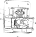
- a charging socket structure with an embedded circuit board includes a charging socket front body 1 and a terminal 3.
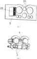
- the charging socket structure with an embedded circuit board further includes a circuit board 2, the circuit board 2 is provided with a terminal mounting through hole 21, the terminal 3 runs through the terminal mounting through hole 21, and the circuit board 2 is provided with an electronic component and a communication interface, as shown in FIGs. 1 to 5 .
- This design greatly reduces the number of outgoing wires inside a charging structure, reducing a diameter of a charging cable. This facilitates design and development work of the vehicle charging socket and mounting, allowing for automatic assembly and reducing costs.
- the electronic component and the communication interface are in parallel relationship, and the electronic component and the communication interface are electrically connected via a circuit wire in a circuit board 2 (for example, a PCB).
- a circuit board 2 for example, a PCB.
- the communication interface is directly connected to the circuit board, avoiding connection of the cables arranged in the charging socket, and the communication interface requires only one opening of a back cover, facilitating sealing of the back cover of the charging socket.
- the circuit board 2 is provided with the terminal mounting through hole 21, and the terminal 3 runs through the terminal mounting through hole 21. This can reduce the mounting space of the circuit board 2 in the charging socket.
- an elastic piece 23 on the circuit board 2 can enable the terminal 3 to be aligned automatically and accurately, reducing eccentricity after insertion of the terminal 3.
- the charging socket front body 1 includes a rear panel 11 and a terminal protection housing 12 arranged in front and rear, the rear panel 11 is provided with a charging socket front body interface 15, the terminal 3 and the charging socket front body interface 15 are connected in one-to-one correspondence, and the circuit board 2 is appropriately disposed in the terminal protection housing 12.
- the terminal protection housing 12 can protect the terminal 3, and after the terminal 3 is connected to the charging socket front body interface 15, a distance between the terminal 3 and the charging socket front body interface 15 is relatively fixed, facilitating insertion into a rear body of the charging socket.
- the size and specification of the charging socket front body interface 15 conform to various standards of Chinese standard AC interface, Chinese standard DC interface, European standard AC interface, European standard DC interface, American standard AC interface, American standard DC interface, Japanese standard AC interface, Japanese standard DC interface, or supercharging interface.
- the charging socket front body 1 may have an irregular contour to match different vehicle models.
- the material of the charging socket front body 1 is insulating soft/hard-plastic material.
- the charging socket front body 1 may be formed through injection molding process, with the smallest draft angle of 0°.
- the terminal protection housing 12 is tube-shaped, and the circuit board 2 is appropriately disposed in the terminal protection housing 12, that is, the external shape of the circuit board 2 matches the interior of the terminal protection housing 12.
- the electronic component includes a temperature sensor, and the temperature sensor is in direct or indirect contact with the terminal 3.
- the temperature sensor can measure the temperature of the terminal 3 and transmit it via a data wire. When the temperature of the terminal 3 is abnormal, the working personnel can deal with it in time.
- the temperature sensor is an NTC temperature sensor or a PTC temperature sensor.
- the two types of temperature sensors have advantages of a small volume, such that a gap that cannot be measured by another thermometer can be measured; convenient use, for a resistance can be arbitrarily selected in a range of 0.1 kQ-100 kQ; and shapes that are easily processed to be complex, allowing for mass production. And these sensors have good stability and strong overload capacity, and are suitable for products such as adapters that require small size and stable performance.
- the circuit board 2 is provided with a temperature sensor, which is in direct or indirect connection with the terminal 3, allowing for more accurate measurement of real-time temperature of the terminal 3 and facilitating disassembly of the terminal 3, thus avoiding that mounting the temperature sensor on the terminal 3 causes difficulties in mounting and disassembly.
- the communication interface is located on a surface of the circuit board 2 back away from the rear panel 11, and the communication interface includes one or more of a pin connector 22, a USB interface, an Ethernet interface, and a wireless interface.
- the communication interface is a pin connector 22, the pin connector 22 may be a single-pin or multi-pin connector, and a male or female contact of the pin connector 22 is disposed on the circuit board 2.
- the communication interface is located at an edge of the circuit board 2, which is conducive to bundling up the cables on the terminal 3.
- the communication interface is located on an upper side, a lower side, a left side, or a right side of the circuit board 2, as shown in FIG. 3 .
- the circuit board 2 is provided with at least one elastic piece 23. As shown in FIG.5 , a periphery of the terminal 3 is connected to the elastic piece 23, and a pressure applied by the elastic piece 23 to the terminal 3 is 3 N 200 N
- the terminal 3 may be in clearance fit with the terminal mounting through hole 21, and the elastic piece 23 is disposed on an external portion of the mounting through hole 21.
- the terminal 3 is connected to the elastic piece 23, and the elastic piece 23 is configured to mount and fix the terminal 3.
- an even number of elastic pieces 23 are provided symmetrically, such that the terminal 3 bears force uniformly in all directions, so as to be connected to the mounting hole 21 more stably.
- the elastic piece 23 is a metal elastic piece, the metal elastic piece is connected to a circuit in the circuit board 2, and the circuit is connected to required electronic components.
- the state (for example, information about current and temperature) of the terminal 3 can be monitored in real time using the electronic components and the metal elastic pieces, and the state information of the terminal 3 can be transmitted outward using the circuit board 2 and the charging cables.
- the method for testing the contact resistance A micro-ohmmeter is used with one end of the test end connected to the terminal 3 and the other end connected to the elastic piece 23, with a same placement position for testing each time, and then the contact resistance on the micro-ohmmeter is obtained.
- a contact resistance greater than 1 mQ is considered as unqualified.
- Table 1 Effects of different pressures on contact resistance Pressure applied by elastic piece to terminal (N) 1 3 8 20 40 60 80 10 0 12 0 14 0 16 0 18 0 200 200 240 260
- Contact resistance between elastic piece and terminal (mQ) 1.2 2 0.9 9 0.9 8 0.9 1 0.8 8 0.8 4 0.8 2 0.7 7 0.7 2 0.6 8 0.6 3 0.5 8 0.5 1 0.49 0.49 0.49 0.49
- the size and specification of the terminal mounting through hole 21 conform to various standards of Chinese standard AC interface, Chinese standard DC interface, European standard AC interface, European standard DC interface, American standard AC interface, American standard DC interface, Japanese standard AC interface, Japanese standard DC interface, or supercharging interface.
- the size and specification of the terminal 3 should also conform to various standards of Chinese standard AC interface, Chinese standard DC interface, European standard AC interface, European standard DC interface, American standard AC interface, American standard DC interface, Japanese standard AC interface, Japanese standard DC interface, or supercharging interface.
- the electronic component further includes a current sensor, and the current sensor is electrically connected to the metal elastic piece.
- the current sensor can check the currents at the terminal 3 and the metal elastic piece 23, allowing the working personnel to know whether the circuit transmission is normal.
- the circuit board is provided with a metal elastic piece, which is directly connected to the terminal, and the other end is connected to a current sensor of the circuit board, allowing for more direct and accurate measurement of the current of the terminal. This also facilitates disassembly of the terminal, avoiding that mounting the current sensor on the terminal causes difficulties in mounting and disassembly.
- the terminal protection housing 12 includes an upper shell 13 and a lower shell 14 arranged up and down.
- the circuit board 2 may be appropriately arranged in the upper shell 13, the circuit board 2 may be appropriately arranged in the lower shell 14 (as shown in FIG. 1 ), or the circuit board 2 may be appropriately arranged in the upper shell 13 and the lower shell 14, as shown in FIGs. 1 to 3 .
- the upper shell 13 and the lower shell 14 can separately protect terminals 3 in different types, facilitating mounting and management.
- the charging socket structure with an embedded circuit board and the charging socket further include a terminal bracket 4.
- the terminal 3 is integrated into a unitary terminal assembly using the terminal bracket 4 (the terminal bracket 4 may be not used alternatively).
- the circuit board 2 is located between the terminal bracket 4 and the rear panel 11, a spacing is present between an inner surface of the terminal protection housing 12 and the terminal bracket 4, and the communication interface is located within the spacing.
- the electronic component on the circuit board 2 may face the rear panel 11 or the terminal bracket 4.
- the spacing is present between the inner surface of the terminal protection housing 12 and the terminal bracket 4, and the communication interface is located within the spacing.
- the communication interface is located on the left side or right side of the circuit board 2, and the circuit board 2 and the communication interface are not sealed and not protected by the terminal bracket 4.
- the circuit board 2 is connected to the rear panel 11 through one or more of adhesive connection, magnetic connection, snap connection, latch connection, bundling connection, threaded connection, rivet connection, and welding connection.
- contact surfaces of the circuit board 2 and the rear panel 11 are provided with adhesive layers through which the circuit board 2 is adhered to the rear panel 11.
- the contact surfaces of the circuit board 2 and the rear panel 11 are provided with magnetic components, and the two are connected through the magnetic force between the magnetic components, allowing for convenient and quick connection.
- one is provided with a snap gripper, and the other is provided with a slot.
- the circuit board 2 is stably connected to the rear panel 11.
- one is provided with a latch, and the other is provided with a clasp.
- the circuit board 2 is stably connected to the rear panel 11.
- the circuit board 2 and the rear panel 11 are both provided with a groove, and after contact surfaces of the two are connected, a bundling member is used to bundle the circuit board 2 and the rear panel 11 at the position of the grooves.
- the bundling member includes a bundling tie, a band clamp, a hook lock, or the like.
- the circuit board 2 and the rear panel 11 are respectively provided with a thread and a screw. Through threaded connection between the thread and the screw, the contact surfaces of the circuit board 2 and the rear panel 11 are connected stably.
- the circuit board 2 and the rear panel 11 are both provided with a connection hole, and a rivet is used with an end passing through the connection holes and then deformed, tightening the connection holes, such that the circuit board 2 and the rear panel 11 are connected stably.
- the circuit board 2 and the rear panel 11 further have welding surfaces.
- a welder is used to melt the welding surfaces for connection, thus allowing the contact surfaces of the circuit board 2 and the rear panel 11 to be connected stably.
- the welder includes a hot melting welder, an ultrasonic welder, or the like.
- the charging socket structure with an embedded circuit board further includes a charging socket rear body.
- the charging socket front body 1 is assembled with the charging socket rear body horizontally; the charging socket front body 1 may be detachably connected to the charging socket rear body for mounting.
- the material of the terminal 3 may be copper or copper alloy, which has good electric conducting property and good elastic property.
- the price of copper continues to rise, the cost of using copper as the material of the terminal 3 becomes increasingly high.
- the percentage of metal aluminum in the earth crust is about 7.73%, and with optimized refining technology, its price is relatively low.
- aluminum is lighter in weight, has the second highest conductivity after copper, and can partially replace copper in the electrical connection field.
- Aluminum or aluminum alloy which has good electric conducting property and average elastic property but is less expensive, may be also selected.
- the material of the terminal 3 When a copper alloy is selected as the material of the terminal 3, it is preferable to include tellurium in the copper to provide terminal 3 with good conductivity and machinability, ensuring electrical performance and improving processability. Additionally, the elasticity of the tellurium copper alloy is also good.
- a percentage of tellurium is 0.1%-5%, further exemplarily, 0.2%-1.2%.
- Each terminal 3 is made of the tellurium copper alloy; mass percentages of tellurium are respectively 0.05%, 0.1%, 0.2%, 1%, 1.2%, 1.8%, 3%, 5%, 6%, and 7%.
- the test results are shown in Table 2.
- Table 2 Effects of tellurium copper alloys with different tellurium percentages on conductivity Tellurium percentage 0.05% 0.1% 0.2% 1% 1.2% 1.8% 3% 5% 6% 7% Conductivit y 98.8% 99.4% 99.6% 99.7% 99.8% 99.6% 99.3% 99.1% 98.7% 98.5%
- the tellurium percentage is less than 0.1% or greater than 5%, the conductivity significantly decreases and the actual requirement cannot be met.
- the mass percentage of tellurium is greater than or equal to 0.2% and less than or equal to 1.2%, the electric conducting property is optimal. Therefore, the inventor selects the tellurium copper alloy with a tellurium percentage of 0. 1%-5%. In the most ideal scenario, the tellurium copper alloy with a tellurium percentage of 0.2%-1.2% is selected as the material of the terminal 3.
- At least part of the terminal 3 in this embodiment is provided with a coating; the coating can improve the corrosion resistance, improve the electric conducting property, increase the number of insertions, and effectively prolong the service life of the terminal.
- the coating may be formed using methods such as electroplating, chemical plating, magnetron sputtering, or vacuum deposition.
- the electroplating method is a process where according to the principle of electrolysis, a thin layer of another metal or alloy is applied onto the surface of a metal.
- the chemical plating method is a process where under the catalytic action of the metal, metal deposition occurs through controlled oxidation-reduction reaction.
- the magnetron sputtering method Through interaction between a magnetic field and an electric field, electrons are enabled to spiral near a target surface, thereby increasing the probability of electron collision with argon gas to produce ions. The generated ions collide with the target surface under the action of the electric field, thereby sputtering into a target material.
- the vacuum deposition method Under a vacuum condition, various metal and non-metal films are deposited on the surface of parts through evaporation, sputtering, or the like.
- the coating is made of one or more of gold, silver, nickel, tin, tin-lead alloy, zinc, silver-antimony alloy, palladium, palladium-nickel alloy, graphite silver, graphene silver, and silver-gold-zirconium alloy.
- Copper or aluminum, as an active metal undergo oxidation reaction with oxygen and water during use. Therefore, one or more inert metals are needed as coatings to prolong the service life of the terminal 3.
- a good, wear-resistant metal is required as a coating, which can greatly prolong the service life of the contacts.
- the contacts require good electric conducting property.
- the electric conducting property and stability of the foregoing metals are superior to those of copper or copper alloys, and aluminum or aluminum alloys, allowing the terminal 3 to achieve better electrical performance and a longer service life.
- the inventor uses sample pieces of the terminals 3, with the same specification, made of the same material but with different coating materials, and performs a test on plug-in and unplug-in times and a test on corrosion resistance time on terminals with the same specification at the plug end.
- the test results are shown in Table 3.
- the plug-in and unplug-in times in Table 3 are obtained as follows: A terminal 3 and a terminal at the plug end are respectively fixed on a test platform, and a mechanical apparatus is used to simulate plug-in and unplug-in of the terminal 3 from the terminal at the plug end. The test is stopped after plug-in and unplug-in every 100 times, to observe the damage situation of the coating on the surface of the terminal 3. If the coating on the surface of the terminal 3 is scratched and the inner material of the terminal 3 is exposed, the test is stopped to record the plug-in and unplug-in times at that moment. In this embodiment, the number of the plug-in and unplug-in times less than 8000 is considered as unqualified.
- the test for corrosion resistance time in Table 3 The terminal 3 is placed in a salt mist spray test box, and a salt mist is sprayed onto various positions of the terminal 3, which is then taken out every 20 hours to be cleaned, and observe the corrosion situation on the surface of the terminal 3. This is a cycle.
- the corrosion area of the surface of the terminal 3 is greater than 10% of the total area, the test is stopped and the cycle number at that moment is recorded. In this embodiment, the cycle number less than 80 times is considered as unqualified.
- Table 3 Effects of different coating materials on plug-in and unplug-in times and corrosion resistance performance of the terminal Different coating materials Gold Silver Nick el Tin Tin-lead alloy Zinc Silverantimo ny alloy Palladi um Palladi umnickel alloy Graph ite silver Graph ene silver Silver -goldzircon ium alloy Plug-in and unplug-in times (times) 12500 11800 9500 9300 9800 9500 12200 12100 12200 12500 12000 10000 Corrosion resistance test cycle (times) 135 120 92 86 89 95 126 118 121 125 130 133
- the present disclosure further discloses a charging socket including the charging socket structure with an embedded circuit board.
- the charging socket front body 1 and the charging socket rear body are both molded through plastic injection.
- the equipment precision and the mold error are controlled to meet the dimensional requirements.
- the injection molding process is controlled based on clamping force, injection position measurement accuracy, injection speed, injection pressure, mold temperature, and the like, thus meeting the dimensional accuracy requirements for preassembly and rotation, as well as the operational requirement for rotational force.
Landscapes
- Engineering & Computer Science (AREA)
- Power Engineering (AREA)
- Transportation (AREA)
- Mechanical Engineering (AREA)
- Details Of Connecting Devices For Male And Female Coupling (AREA)
- Charge And Discharge Circuits For Batteries Or The Like (AREA)
- Connector Housings Or Holding Contact Members (AREA)
- Coupling Device And Connection With Printed Circuit (AREA)
Abstract
Description
- This application claims the priority to
Chinese Patent Application No. 202122683238.7, titled "CHARGING SOCKET STRUCTURE WITH EMBEDDED CIRCUIT BOARD AND CHARGING SOCKET", and filed on November 4, 2021 - The present disclosure relates to the field of charging technologies, and in particular to a charging socket structure with an embedded circuit board and a charging socket including the charging socket structure with an embedded circuit board.
- The batteries of new energy vehicles rely on the charging system to replenish power. The charging socket in the charging system includes multiple charging terminals and cables. The charging terminals and cables are connected in the charging socket, with the charging terminals fixed onto the charging socket body and the cables running through a back cover. During the development and assembly of a charging socket of the electric vehicle, because some of various electronic components in the charging socket need to communicate interactively with the vehicle, a rear panel of the charging socket needs to be provided with corresponding openings. In addition, the charging cable may have an excessively large diameter due to too many connected wires, leading to resource waste, difficulties in sealing, and certain safety risk.
- Additionally, the terminal in the charging socket needs to be as concentric as possible with a terminal mounting cavity, ensuring that when aligned with a charging gun, the terminal can be accurately inserted into the gun in one attempt without the deviation case. Currently, the terminals in charging sockets are fixed in place, which leads to a problem known as "contagious failure" where the terminals of charging guns from different manufacturers become ineffective. Alternatively, terminals are mounted with large clearances, but this leads to relatively serious wear on the terminals and increases the frequency of replacements.
- Therefore, a new solution is needed urgently to address the foregoing problems in the prior art.
- To conveniently mount electronic components in a charging socket, the present disclosure provides a charging socket structure with an embedded circuit board and a charging socket. The charging socket structure with an embedded circuit board includes a circuit board, and the circuit board is integrated with various types of electronic components. The circuit board, through integration connection, greatly reduces outgoing wires inside a charging structure, reducing a diameter of a charging cable. This facilitates design and development work of the vehicle charging socket, reducing costs.
- To resolve the technical problems, the present disclosure uses the following technical solution:
- The charging socket structure with an embedded circuit board includes a charging socket front body and a terminal. The charging socket structure with an embedded circuit board further includes a circuit board, the circuit board is provided with a terminal mounting through hole, the terminal runs through the terminal mounting through hole, and the circuit board is provided with an electronic component and a communication interface.
- The charging socket includes the foregoing charging socket structure with an embedded circuit board.
- The present disclosure has the following beneficial effects:
- 1. The charging socket structure with an embedded circuit board includes the circuit board, allowing for integration of various types of electronic components on the circuit board. The circuit board, through integration connection, greatly reduces outgoing wires inside a charging structure, reducing a diameter of a charging cable. This facilitates design and development work of the vehicle charging socket and mounting, allowing for automatic assembly and reducing costs.
- 2. The communication interface is directly connected to the circuit board, avoiding connection of the cables arranged in the charging socket, and the communication interface requires only one opening of a back cover, facilitating sealing of the back cover of the charging socket.
- 3. The circuit board is provided with the terminal mounting through hole, and the terminal runs through the terminal mounting through hole. This can reduce the mounting space of the circuit board in the charging socket. In addition, an elastic piece on the circuit board can enable the terminal to be aligned automatically and accurately, reducing eccentricity after insertion of the terminal.
- 4. The circuit board is provided with a metal elastic piece, which is directly connected to the terminal, and the other end is connected to a current sensor of the circuit board, allowing for more direct and accurate measurement of the current of the terminal. This also facilitates disassembly of the terminal, avoiding that mounting the current sensor on the terminal causes difficulties in mounting and disassembly.
- 5. The circuit board is provided with a temperature sensor, which is in direct or indirect connection with the terminal, allowing for more accurate measurement of real-time temperature of the terminal and facilitating disassembly of the terminal, thus avoiding that mounting the temperature sensor on the terminal causes difficulties in mounting and disassembly.
- The accompanying drawings of the specification forming a part of this application are provided for a better understanding of the present disclosure. The exemplary embodiments and their descriptions in the present disclosure are intended for explaining the present disclosure and do not constitute a limitation on the present disclosure.
-
FIG. 1 is a schematic diagram of a charging socket structure with an embedded circuit board according to the present disclosure. -
FIG. 2 is a schematic diagram of a charging socket front body. -
FIG. 3 is a schematic diagram of a circuit board. -
FIG. 4 is a schematic diagram of a unitary terminal assembly. -
FIG. 5 is a schematic structural diagram of an elastic piece. - Numeral references: 1. charging socket front body; 2. circuit board; 3. terminal; 4. terminal bracket;
- 11. rear panel; 12. terminal protection housing; 13. upper shell; 14. lower shell; 15. charging socket front body interface;
- 21. mounting through hole; 22. pin connector; and 23. elastic piece.
- It should be noted that, in the absence of a conflict, embodiments of this application can be combined with features in the embodiments. The present disclosure is described in detail below with reference to accompanying drawings and embodiments.
- A charging socket structure with an embedded circuit board includes a charging
socket front body 1 and aterminal 3. The charging socket structure with an embedded circuit board further includes acircuit board 2, thecircuit board 2 is provided with a terminal mounting throughhole 21, the terminal 3 runs through the terminal mounting throughhole 21, and thecircuit board 2 is provided with an electronic component and a communication interface, as shown inFIGs. 1 to 5 . This design greatly reduces the number of outgoing wires inside a charging structure, reducing a diameter of a charging cable. This facilitates design and development work of the vehicle charging socket and mounting, allowing for automatic assembly and reducing costs. - In some embodiments that, the electronic component and the communication interface are in parallel relationship, and the electronic component and the communication interface are electrically connected via a circuit wire in a circuit board 2 (for example, a PCB). Those of ordinary skill in the art may choose to install the electronic component based on requirements, to reduce outgoing wires in the charging structure, thus reducing a diameter of a charging cable. The communication interface is directly connected to the circuit board, avoiding connection of the cables arranged in the charging socket, and the communication interface requires only one opening of a back cover, facilitating sealing of the back cover of the charging socket.
- The
circuit board 2 is provided with the terminal mounting throughhole 21, and the terminal 3 runs through the terminal mounting throughhole 21. This can reduce the mounting space of thecircuit board 2 in the charging socket. In addition, anelastic piece 23 on thecircuit board 2 can enable theterminal 3 to be aligned automatically and accurately, reducing eccentricity after insertion of theterminal 3. - In this embodiment, the charging
socket front body 1 includes arear panel 11 and aterminal protection housing 12 arranged in front and rear, therear panel 11 is provided with a charging socketfront body interface 15, theterminal 3 and the charging socketfront body interface 15 are connected in one-to-one correspondence, and thecircuit board 2 is appropriately disposed in theterminal protection housing 12. Theterminal protection housing 12 can protect theterminal 3, and after theterminal 3 is connected to the charging socketfront body interface 15, a distance between the terminal 3 and the charging socketfront body interface 15 is relatively fixed, facilitating insertion into a rear body of the charging socket. - The size and specification of the charging socket
front body interface 15 conform to various standards of Chinese standard AC interface, Chinese standard DC interface, European standard AC interface, European standard DC interface, American standard AC interface, American standard DC interface, Japanese standard AC interface, Japanese standard DC interface, or supercharging interface. - The charging
socket front body 1 may have an irregular contour to match different vehicle models. The material of the chargingsocket front body 1 is insulating soft/hard-plastic material. The chargingsocket front body 1 may be formed through injection molding process, with the smallest draft angle of 0°. - In this embodiment, the
terminal protection housing 12 is tube-shaped, and thecircuit board 2 is appropriately disposed in theterminal protection housing 12, that is, the external shape of thecircuit board 2 matches the interior of theterminal protection housing 12. - In this embodiment, the electronic component includes a temperature sensor, and the temperature sensor is in direct or indirect contact with the
terminal 3. The temperature sensor can measure the temperature of theterminal 3 and transmit it via a data wire. When the temperature of theterminal 3 is abnormal, the working personnel can deal with it in time. - The temperature sensor is an NTC temperature sensor or a PTC temperature sensor. The two types of temperature sensors have advantages of a small volume, such that a gap that cannot be measured by another thermometer can be measured; convenient use, for a resistance can be arbitrarily selected in a range of 0.1 kQ-100 kQ; and shapes that are easily processed to be complex, allowing for mass production. And these sensors have good stability and strong overload capacity, and are suitable for products such as adapters that require small size and stable performance.
- The
circuit board 2 is provided with a temperature sensor, which is in direct or indirect connection with theterminal 3, allowing for more accurate measurement of real-time temperature of theterminal 3 and facilitating disassembly of theterminal 3, thus avoiding that mounting the temperature sensor on theterminal 3 causes difficulties in mounting and disassembly. - The communication interface is located on a surface of the
circuit board 2 back away from therear panel 11, and the communication interface includes one or more of apin connector 22, a USB interface, an Ethernet interface, and a wireless interface. - Exemplarily, the communication interface is a
pin connector 22, thepin connector 22 may be a single-pin or multi-pin connector, and a male or female contact of thepin connector 22 is disposed on thecircuit board 2. The communication interface is located at an edge of thecircuit board 2, which is conducive to bundling up the cables on theterminal 3. The communication interface is located on an upper side, a lower side, a left side, or a right side of thecircuit board 2, as shown inFIG. 3 . - In this embodiment, the
circuit board 2 is provided with at least oneelastic piece 23. As shown inFIG.5 , a periphery of theterminal 3 is connected to theelastic piece 23, and a pressure applied by theelastic piece 23 to theterminal 3 is 3 N 200 N - The
terminal 3 may be in clearance fit with the terminal mounting throughhole 21, and theelastic piece 23 is disposed on an external portion of the mounting throughhole 21. Theterminal 3 is connected to theelastic piece 23, and theelastic piece 23 is configured to mount and fix theterminal 3. There may be multipleelastic pieces 23, and theelastic pieces 23 are uniformly distributed around theterminal 3. Exemplarily, an even number ofelastic pieces 23 are provided symmetrically, such that theterminal 3 bears force uniformly in all directions, so as to be connected to the mountinghole 21 more stably. - Exemplarily, the
elastic piece 23 is a metal elastic piece, the metal elastic piece is connected to a circuit in thecircuit board 2, and the circuit is connected to required electronic components. Such design has the advantages: the state (for example, information about current and temperature) of theterminal 3 can be monitored in real time using the electronic components and the metal elastic pieces, and the state information of theterminal 3 can be transmitted outward using thecircuit board 2 and the charging cables. - To figure out effects of a pressure applied by the
elastic piece 23 to theterminal 3 on a contact resistance and unplug-in situation of the insertedterminal 3, the inventor selects terminal mounting throughholes 21 andterminals 3 separately with the same size and specification, and differentelastic pieces 23 applying pressures to theterminals 3, selects thesame terminals 3 for insertion, and tests a contact resistance between an insertedterminal 3 and anelastic piece 23. The test results are shown in Table 1. - The method for testing the contact resistance: A micro-ohmmeter is used with one end of the test end connected to the
terminal 3 and the other end connected to theelastic piece 23, with a same placement position for testing each time, and then the contact resistance on the micro-ohmmeter is obtained. In this embodiment, a contact resistance greater than 1 mQ is considered as unqualified.Table 1: Effects of different pressures on contact resistance Pressure applied by elastic piece to terminal (N) 1 3 8 20 40 60 80 10 0 12 0 14 0 16 0 18 0 200 200 240 260 Contact resistance between elastic piece and terminal (mQ) 1.2 2 0.9 9 0.9 8 0.9 1 0.8 8 0.8 4 0.8 2 0.7 7 0.7 2 0.6 8 0.6 3 0.5 8 0.5 1 0.49 0.49 0.49 - It can be known from Table 1 that when the pressure applied by the
elastic piece 23 to theterminal 3 is less than 3 N, the contact resistance between the terminal 3 and theelastic piece 23 is greater than 1 mΩ, which is excessively large. When the pressure applied by theelastic piece 23 to theterminal 3 is greater than 200 N, the resistance cannot be further reduced and unplug-in is more difficult. Therefore, the inventor sets the pressure applied by theelastic piece 23 to theterminal 3 to 3 N 200 N. - In this embodiment, the size and specification of the terminal mounting through
hole 21 conform to various standards of Chinese standard AC interface, Chinese standard DC interface, European standard AC interface, European standard DC interface, American standard AC interface, American standard DC interface, Japanese standard AC interface, Japanese standard DC interface, or supercharging interface. - Because the
terminals 3 are inserted into the terminal mounting throughholes 21 in one-to-one correspondence, the size and specification of theterminal 3 should also conform to various standards of Chinese standard AC interface, Chinese standard DC interface, European standard AC interface, European standard DC interface, American standard AC interface, American standard DC interface, Japanese standard AC interface, Japanese standard DC interface, or supercharging interface. - In this embodiment, the electronic component further includes a current sensor, and the current sensor is electrically connected to the metal elastic piece. The current sensor can check the currents at the
terminal 3 and the metalelastic piece 23, allowing the working personnel to know whether the circuit transmission is normal. The circuit board is provided with a metal elastic piece, which is directly connected to the terminal, and the other end is connected to a current sensor of the circuit board, allowing for more direct and accurate measurement of the current of the terminal. This also facilitates disassembly of the terminal, avoiding that mounting the current sensor on the terminal causes difficulties in mounting and disassembly. - In this embodiment, the
terminal protection housing 12 includes anupper shell 13 and alower shell 14 arranged up and down. Thecircuit board 2 may be appropriately arranged in theupper shell 13, thecircuit board 2 may be appropriately arranged in the lower shell 14 (as shown inFIG. 1 ), or thecircuit board 2 may be appropriately arranged in theupper shell 13 and thelower shell 14, as shown inFIGs. 1 to 3 . Theupper shell 13 and thelower shell 14 can separately protectterminals 3 in different types, facilitating mounting and management. - In this embodiment, the charging socket structure with an embedded circuit board and the charging socket further include a
terminal bracket 4. Theterminal 3 is integrated into a unitary terminal assembly using the terminal bracket 4 (theterminal bracket 4 may be not used alternatively). Thecircuit board 2 is located between theterminal bracket 4 and therear panel 11, a spacing is present between an inner surface of theterminal protection housing 12 and theterminal bracket 4, and the communication interface is located within the spacing. As shown inFIG. 4 , the electronic component on thecircuit board 2 may face therear panel 11 or theterminal bracket 4. The spacing is present between the inner surface of theterminal protection housing 12 and theterminal bracket 4, and the communication interface is located within the spacing. The communication interface is located on the left side or right side of thecircuit board 2, and thecircuit board 2 and the communication interface are not sealed and not protected by theterminal bracket 4. - In this embodiment, the
circuit board 2 is connected to therear panel 11 through one or more of adhesive connection, magnetic connection, snap connection, latch connection, bundling connection, threaded connection, rivet connection, and welding connection. - In a first feasible technical solution, contact surfaces of the
circuit board 2 and therear panel 11 are provided with adhesive layers through which thecircuit board 2 is adhered to therear panel 11. - In a second feasible technical solution, the contact surfaces of the
circuit board 2 and therear panel 11 are provided with magnetic components, and the two are connected through the magnetic force between the magnetic components, allowing for convenient and quick connection. - In a third feasible technical solution, of the contact surfaces of the
circuit board 2 and therear panel 11, one is provided with a snap gripper, and the other is provided with a slot. Through the assembly of the snap gripper and the slot, thecircuit board 2 is stably connected to therear panel 11. - In a fourth feasible technical solution, of the contact surfaces of the
circuit board 2 and therear panel 11, one is provided with a latch, and the other is provided with a clasp. Through the assembly of the latch and the clasp, thecircuit board 2 is stably connected to therear panel 11. - In a fifth feasible technical solution, the
circuit board 2 and therear panel 11 are both provided with a groove, and after contact surfaces of the two are connected, a bundling member is used to bundle thecircuit board 2 and therear panel 11 at the position of the grooves. The bundling member includes a bundling tie, a band clamp, a hook lock, or the like. - In a sixth feasible technical solution, the
circuit board 2 and therear panel 11 are respectively provided with a thread and a screw. Through threaded connection between the thread and the screw, the contact surfaces of thecircuit board 2 and therear panel 11 are connected stably. - In a seventh feasible technical solution, the
circuit board 2 and therear panel 11 are both provided with a connection hole, and a rivet is used with an end passing through the connection holes and then deformed, tightening the connection holes, such that thecircuit board 2 and therear panel 11 are connected stably. - In an eighth feasible technical solution, in addition to the contact surfaces, the
circuit board 2 and therear panel 11 further have welding surfaces. A welder is used to melt the welding surfaces for connection, thus allowing the contact surfaces of thecircuit board 2 and therear panel 11 to be connected stably. The welder includes a hot melting welder, an ultrasonic welder, or the like. - In this embodiment, the charging socket structure with an embedded circuit board further includes a charging socket rear body. The charging
socket front body 1 is assembled with the charging socket rear body horizontally; the chargingsocket front body 1 may be detachably connected to the charging socket rear body for mounting. - In this embodiment, the material of the
terminal 3 may be copper or copper alloy, which has good electric conducting property and good elastic property. However, as the price of copper continues to rise, the cost of using copper as the material of theterminal 3 becomes increasingly high. The percentage of metal aluminum in the earth crust is about 7.73%, and with optimized refining technology, its price is relatively low. Compared with copper, aluminum is lighter in weight, has the second highest conductivity after copper, and can partially replace copper in the electrical connection field. Aluminum or aluminum alloy, which has good electric conducting property and average elastic property but is less expensive, may be also selected. - When a copper alloy is selected as the material of the
terminal 3, it is preferable to include tellurium in the copper to provide terminal 3 with good conductivity and machinability, ensuring electrical performance and improving processability. Additionally, the elasticity of the tellurium copper alloy is also good. - Exemplarily, in the tellurium copper alloy, a percentage of tellurium is 0.1%-5%, further exemplarily, 0.2%-1.2%.
- The inventor selects 10
terminals 3 in the same shape for test. Eachterminal 3 is made of the tellurium copper alloy; mass percentages of tellurium are respectively 0.05%, 0.1%, 0.2%, 1%, 1.2%, 1.8%, 3%, 5%, 6%, and 7%. The test results are shown in Table 2.Table 2: Effects of tellurium copper alloys with different tellurium percentages on conductivity Tellurium percentage 0.05% 0.1% 0.2% 1% 1.2% 1.8% 3% 5% 6% 7% Conductivit y 98.8% 99.4% 99.6% 99.7% 99.8% 99.6% 99.3% 99.1% 98.7% 98.5% - It can be known from Table 2, when the tellurium percentage is less than 0.1% or greater than 5%, the conductivity significantly decreases and the actual requirement cannot be met. When the mass percentage of tellurium is greater than or equal to 0.2% and less than or equal to 1.2%, the electric conducting property is optimal. Therefore, the inventor selects the tellurium copper alloy with a tellurium percentage of 0. 1%-5%. In the most ideal scenario, the tellurium copper alloy with a tellurium percentage of 0.2%-1.2% is selected as the material of the
terminal 3. - At least part of the
terminal 3 in this embodiment is provided with a coating; the coating can improve the corrosion resistance, improve the electric conducting property, increase the number of insertions, and effectively prolong the service life of the terminal. - The coating may be formed using methods such as electroplating, chemical plating, magnetron sputtering, or vacuum deposition.
- The electroplating method is a process where according to the principle of electrolysis, a thin layer of another metal or alloy is applied onto the surface of a metal.
- The chemical plating method is a process where under the catalytic action of the metal, metal deposition occurs through controlled oxidation-reduction reaction.
- The magnetron sputtering method: Through interaction between a magnetic field and an electric field, electrons are enabled to spiral near a target surface, thereby increasing the probability of electron collision with argon gas to produce ions. The generated ions collide with the target surface under the action of the electric field, thereby sputtering into a target material.
- The vacuum deposition method: Under a vacuum condition, various metal and non-metal films are deposited on the surface of parts through evaporation, sputtering, or the like.
- The coating is made of one or more of gold, silver, nickel, tin, tin-lead alloy, zinc, silver-antimony alloy, palladium, palladium-nickel alloy, graphite silver, graphene silver, and silver-gold-zirconium alloy. Copper or aluminum, as an active metal, undergo oxidation reaction with oxygen and water during use. Therefore, one or more inert metals are needed as coatings to prolong the service life of the
terminal 3. Additionally, for metal contacts that require frequent unplug-in, a good, wear-resistant metal is required as a coating, which can greatly prolong the service life of the contacts. Furthermore, the contacts require good electric conducting property. The electric conducting property and stability of the foregoing metals are superior to those of copper or copper alloys, and aluminum or aluminum alloys, allowing theterminal 3 to achieve better electrical performance and a longer service life. - To figure out effects of different coating materials on overall performance of the
terminal 3, the inventor uses sample pieces of theterminals 3, with the same specification, made of the same material but with different coating materials, and performs a test on plug-in and unplug-in times and a test on corrosion resistance time on terminals with the same specification at the plug end. The test results are shown in Table 3. - The plug-in and unplug-in times in Table 3 are obtained as follows: A
terminal 3 and a terminal at the plug end are respectively fixed on a test platform, and a mechanical apparatus is used to simulate plug-in and unplug-in of the terminal 3 from the terminal at the plug end. The test is stopped after plug-in and unplug-in every 100 times, to observe the damage situation of the coating on the surface of theterminal 3. If the coating on the surface of theterminal 3 is scratched and the inner material of theterminal 3 is exposed, the test is stopped to record the plug-in and unplug-in times at that moment. In this embodiment, the number of the plug-in and unplug-in times less than 8000 is considered as unqualified. - The test for corrosion resistance time in Table 3: The
terminal 3 is placed in a salt mist spray test box, and a salt mist is sprayed onto various positions of theterminal 3, which is then taken out every 20 hours to be cleaned, and observe the corrosion situation on the surface of theterminal 3. This is a cycle. When the corrosion area of the surface of theterminal 3 is greater than 10% of the total area, the test is stopped and the cycle number at that moment is recorded. In this embodiment, the cycle number less than 80 times is considered as unqualified.Table 3: Effects of different coating materials on plug-in and unplug-in times and corrosion resistance performance of the terminal Different coating materials Gold Silver Nick el Tin Tin-lead alloy Zinc Silverantimo ny alloy Palladi um Palladi umnickel alloy Graph ite silver Graph ene silver Silver -goldzircon ium alloy Plug-in and unplug-in times (times) 12500 11800 9500 9300 9800 9500 12200 12100 12200 12500 12000 10000 Corrosion resistance test cycle (times) 135 120 92 86 89 95 126 118 121 125 130 133 - It can be seen from Table 3 that when the coatings are made of gold, silver, silver-antimony alloy, palladium, palladium-nickel alloy, graphite silver, graphene silver, and silver-gold-zirconium alloy, most of the values in the rest results exceed the standard values, showing stable performance. When the coatings are made of nickel, tin, tin-lead alloy, and zinc, the test results also meet the requirements. Therefore, the inventor selects one or more of the following as the material of the coating: gold, silver, nickel, tin, tin-lead alloy, zinc, silver-antimony alloy, palladium, palladium-nickel alloy, graphite silver, graphene silver, and silver-gold-zirconium alloy.
- The present disclosure further discloses a charging socket including the charging socket structure with an embedded circuit board.
- The following describes the processing and molding of the charging
socket front body 1 and the charging socket rear body:
The chargingsocket front body 1 and the charging socket rear body are both molded through plastic injection. The equipment precision and the mold error are controlled to meet the dimensional requirements. The injection molding process is controlled based on clamping force, injection position measurement accuracy, injection speed, injection pressure, mold temperature, and the like, thus meeting the dimensional accuracy requirements for preassembly and rotation, as well as the operational requirement for rotational force. - The specific parameters are as follows:
- 0.03 mm is taken when the clamping force is zero; and 0.005 mm is taken when the clamping force is maximum;
- the injection position accuracy (end of packing) is less than 0.03 mm;
- the injection speed is greater than or equal to 300 mm/s;
- the injection pressure is greater than 25 MPa; and
- the temperature variation of the mold is controlled within ±1°C.
- The following describes the comparison of technical effects between the charging socket structure with an embedded circuit board of the present disclosure and the conventional charging socket. See Table 4.
Table 4: A comparison of technical effects between the charging socket structure with an embedded circuit board of the present disclosure and the conventional charging socket Prior art The present disclosure The number of outgoing wires of a circuit board At least two outgoing wires Only one outgoing wire Waterproof and sealing performance Multiple sealed parts with a poor effect Only one part sealed, reducing probability of failure, exerting significant effect Safety and convenience Too many outgoing wires result in inconvenient mounting Automatic assembly process can be achieved, facilitating mounting - For the sake of understanding and description, absolute positional relationships are used in the present disclosure. Unless otherwise specified, in
FIG. 1 , the directional term "up" refers to the upper direction, "down" refers to the lower direction, and "left" refers to the left direction, "right" refers to the right direction, "front" refers to a direction perpendicular to a paper surface inFIG. 1 and pointing an inner side of the paper surface, and "back" refers to a direction perpendicular to a paper surface inFIG. 1 and pointing an outer side of the paper surface. The present disclosure is described from the observer's perspective, but the directional terms mentioned above should not be construed or interpreted as limitations to the scope of protection of the present disclosure. - The foregoing descriptions are merely specific embodiments of the present disclosure and cannot be used to limit the implementation scope of the present disclosure. Therefore, equivalent substitutions of assemblies or equivalent changes and modifications made within the protection scope of the present disclosure should be covered by the present disclosure. Additionally, the technical features, the technical features and the technical solutions, and the technical solutions in the present disclosure all can be combined arbitrarily for use.
Claims (11)
- A charging socket structure with an embedded circuit board, comprising a charging socket front body (1) and a terminal (3), in characterized that, the charging socket structure with an embedded circuit board further comprises a circuit board (2), the circuit board (2) is provided with a terminal mounting through hole (21), the terminal (3) runs through the terminal mounting through hole (21), and the circuit board (2) is provided with an electronic component and a communication interface.
- The charging socket structure with an embedded circuit board according to claim 1, in characterized that, the charging socket front body (1) comprises a rear panel (11) and a terminal protection housing (12) arranged in front and rear, the rear panel (11) is provided with a charging socket front body interface (15), the terminal (3) and the charging socket front body interface (15) are connected in one-to-one correspondence, and the circuit board (2) is appropriately disposed in the terminal protection housing (12).
- The charging socket structure with an embedded circuit board according to claim 1, in characterized that, the electronic component comprises a temperature sensor, and the temperature sensor is in direct or indirect contact with the terminal (3).
- The charging socket structure with an embedded circuit board according to claim 2, in characterized that, the communication interface is located on a surface of the circuit board (2) back away from the rear panel (11), and the communication interface comprises one or more of a pin connector (22), a USB interface, an Ethernet interface, and a wireless interface.
- The charging socket structure with an embedded circuit board according to claim 1, in characterized that, the circuit board (2) is provided with at least one elastic piece (23), a periphery of the terminal (3) is connected to the elastic piece (23), and a pressure applied by the elastic piece (23) to the terminal (3) is 3 N 200 N.
- The charging socket structure with an embedded circuit board according to claim 5, in characterized that, the elastic piece (23) is a metal elastic piece, and the metal elastic piece is connected to a circuit in the circuit board (2).
- The charging socket structure with an embedded circuit board according to claim 6, in characterized that, the electronic component comprises a current sensor, and the current sensor is electrically connected to the metal elastic piece.
- The charging socket structure with an embedded circuit board according to claim 2, wherein the terminal protection housing (12) comprises an upper shell (13) and a lower shell (14) arranged up and down, the circuit board (2) is located in the upper shell (13), the circuit board (2) is located in the lower shell (14), or the circuit board (2) is located in the upper shell (13) and the lower shell (14).
- The charging socket structure with an embedded circuit board according to claim 2, further comprising a terminal bracket (4), wherein the terminal (3) is integrated into a unitary terminal assembly using the terminal bracket (4), the circuit board (2) is located between the terminal bracket (4) and the rear panel (11), a spacing is present between an inner surface of the terminal protection housing (12) and the terminal bracket (4), and the communication interface is located within the spacing.
- The charging socket structure with an embedded circuit board according to claim 2, in characterized that, the circuit board (2) is connected to the rear panel (11) through one or more of adhesive connection, magnetic connection, snap connection, insertion connection, latch connection, bundling connection, threaded connection, rivet connection, and welding connection.
- A charging socket, in characterized that, comprising the charging socket structure with an embedded circuit board according to any one of claims 1 to 10.
Applications Claiming Priority (2)
| Application Number | Priority Date | Filing Date | Title |
|---|---|---|---|
| CN202122683238.7U CN216085425U (en) | 2021-11-04 | 2021-11-04 | Charging seat structure and charging seat of embedded circuit board |
| PCT/CN2022/129021 WO2023078247A1 (en) | 2021-11-04 | 2022-11-01 | Charging socket structure with embedded circuit board, and charging socket |
Publications (2)
| Publication Number | Publication Date |
|---|---|
| EP4429035A1 true EP4429035A1 (en) | 2024-09-11 |
| EP4429035A4 EP4429035A4 (en) | 2025-03-26 |
Family
ID=80644057
Family Applications (1)
| Application Number | Title | Priority Date | Filing Date |
|---|---|---|---|
| EP22889271.7A Pending EP4429035A4 (en) | 2021-11-04 | 2022-11-01 | Charging socket structure with embedded circuit board, and charging socket |
Country Status (4)
| Country | Link |
|---|---|
| EP (1) | EP4429035A4 (en) |
| JP (1) | JP3248874U (en) |
| CN (1) | CN216085425U (en) |
| WO (1) | WO2023078247A1 (en) |
Cited By (1)
| Publication number | Priority date | Publication date | Assignee | Title |
|---|---|---|---|---|
| TWI893989B (en) * | 2024-09-19 | 2025-08-11 | 大陸商江陰信承電子有限公司 | Modular charging connector |
Families Citing this family (4)
| Publication number | Priority date | Publication date | Assignee | Title |
|---|---|---|---|---|
| CN216085425U (en) * | 2021-11-04 | 2022-03-18 | 长春捷翼汽车零部件有限公司 | Charging seat structure and charging seat of embedded circuit board |
| CN217823383U (en) * | 2022-04-22 | 2022-11-15 | 长春捷翼汽车零部件有限公司 | PCB and shell integrated structure |
| CN115332835A (en) * | 2022-08-16 | 2022-11-11 | 长春捷翼汽车零部件有限公司 | Connector combination and charging device |
| CN116960669B (en) * | 2023-06-09 | 2024-05-17 | 武汉德泰纳新能源技术有限公司 | New energy automobile charging seat |
Family Cites Families (7)
| Publication number | Priority date | Publication date | Assignee | Title |
|---|---|---|---|---|
| JP2001178001A (en) * | 1999-12-16 | 2001-06-29 | Toyota Autom Loom Works Ltd | Vehicle charging device |
| JP5842187B2 (en) * | 2011-06-16 | 2016-01-13 | 株式会社Braveridge | Connecting parts and charger for charging |
| CN207052813U (en) * | 2017-05-12 | 2018-02-27 | 泰科电子(上海)有限公司 | Socket casing component and socket |
| BE1026857B1 (en) * | 2018-12-10 | 2020-07-13 | Phoenix Contact E Mobility Gmbh | Connector part with a circuit board |
| CN210629971U (en) * | 2019-06-28 | 2020-05-26 | 深圳威迈斯新能源股份有限公司 | Mounting structure of PCB (printed circuit board) for vehicle-mounted charger and voltage converter |
| CN211405514U (en) * | 2019-11-08 | 2020-09-01 | 诺莱德(上海)汽车科技有限公司 | DC charging seat with integrated circuit |
| CN216085425U (en) * | 2021-11-04 | 2022-03-18 | 长春捷翼汽车零部件有限公司 | Charging seat structure and charging seat of embedded circuit board |
-
2021
- 2021-11-04 CN CN202122683238.7U patent/CN216085425U/en active Active
-
2022
- 2022-11-01 JP JP2024600061U patent/JP3248874U/en active Active
- 2022-11-01 WO PCT/CN2022/129021 patent/WO2023078247A1/en not_active Ceased
- 2022-11-01 EP EP22889271.7A patent/EP4429035A4/en active Pending
Cited By (1)
| Publication number | Priority date | Publication date | Assignee | Title |
|---|---|---|---|---|
| TWI893989B (en) * | 2024-09-19 | 2025-08-11 | 大陸商江陰信承電子有限公司 | Modular charging connector |
Also Published As
| Publication number | Publication date |
|---|---|
| WO2023078247A1 (en) | 2023-05-11 |
| EP4429035A4 (en) | 2025-03-26 |
| CN216085425U (en) | 2022-03-18 |
| JP3248874U (en) | 2024-10-28 |
Similar Documents
| Publication | Publication Date | Title |
|---|---|---|
| EP4429035A1 (en) | Charging socket structure with embedded circuit board, and charging socket | |
| EP2650972B1 (en) | Crimp terminal, connection structure, and production method for same | |
| EP2631994B1 (en) | Crimped terminal wire for automobiles | |
| EP4398270A1 (en) | Electric energy transmission system for vehicle, and charging apparatus and electric vehicle | |
| EP4383464B1 (en) | Electrical connection structure, charging seat, and automobile | |
| EP4383481B1 (en) | Charging socket and vehicle | |
| TWI587584B (en) | Connector with gold-palladium plated contacts | |
| EP4391242B1 (en) | Plug-in structure of busbar and terminal, and motor vehicle | |
| EP4443670A1 (en) | Automobile charging device and manufacturing method | |
| EP4383469B1 (en) | Charging socket and vehicle | |
| EP4379747A1 (en) | Integrated harness assembly and manufacturing method therefor, automobile, and vehicle | |
| EP4496142A1 (en) | Electric energy transmission connecting device and vehicle | |
| EP4459814A1 (en) | Conveniently replaceable charging socket and vehicle | |
| EP4383465A1 (en) | Electrical connection structure, charging socket and automobile | |
| JP2014525983A (en) | Electrical contact coating | |
| CN113922137A (en) | Connecting mechanism with shielding, electric energy transmission device and motor vehicle | |
| CN103178370B (en) | Parts | |
| EP2702646B1 (en) | Connector assembly and connection system using same | |
| CN217215235U (en) | Connecting mechanism with shielding, electric energy transmission device and motor vehicle | |
| EP4372920A1 (en) | Plug-in terminal, plug-in connection structure, and plug-in terminal assembly | |
| EP4443663B1 (en) | Metal reed structure and electrical connector | |
| EP4415185A1 (en) | Charging connector | |
| EP4391239A1 (en) | Micro-vibration terminal, plug-in structure, and motor vehicle | |
| EP4411996A1 (en) | High-voltage connecting mechanism, electrical energy transmission apparatus, and motor vehicle | |
| EP4411999B1 (en) | Connection mechanism having shield, electric energy transmission apparatus, and motor vehicle |
Legal Events
| Date | Code | Title | Description |
|---|---|---|---|
| STAA | Information on the status of an ep patent application or granted ep patent |
Free format text: STATUS: THE INTERNATIONAL PUBLICATION HAS BEEN MADE |
|
| PUAI | Public reference made under article 153(3) epc to a published international application that has entered the european phase |
Free format text: ORIGINAL CODE: 0009012 |
|
| STAA | Information on the status of an ep patent application or granted ep patent |
Free format text: STATUS: REQUEST FOR EXAMINATION WAS MADE |
|
| 17P | Request for examination filed |
Effective date: 20240513 |
|
| AK | Designated contracting states |
Kind code of ref document: A1 Designated state(s): AL AT BE BG CH CY CZ DE DK EE ES FI FR GB GR HR HU IE IS IT LI LT LU LV MC ME MK MT NL NO PL PT RO RS SE SI SK SM TR |
|
| P01 | Opt-out of the competence of the unified patent court (upc) registered |
Free format text: CASE NUMBER: APP_53693/2024 Effective date: 20240926 |
|
| DAV | Request for validation of the european patent (deleted) | ||
| DAX | Request for extension of the european patent (deleted) | ||
| A4 | Supplementary search report drawn up and despatched |
Effective date: 20250220 |
|
| RIC1 | Information provided on ipc code assigned before grant |
Ipc: H01R 13/66 20060101ALI20250214BHEP Ipc: B60L 53/18 20190101ALI20250214BHEP Ipc: B60L 53/16 20190101ALI20250214BHEP Ipc: H01R 12/71 20110101ALI20250214BHEP Ipc: H01R 13/52 20060101ALI20250214BHEP Ipc: H01R 13/40 20060101AFI20250214BHEP |
|
| GRAP | Despatch of communication of intention to grant a patent |
Free format text: ORIGINAL CODE: EPIDOSNIGR1 |
|
| STAA | Information on the status of an ep patent application or granted ep patent |
Free format text: STATUS: GRANT OF PATENT IS INTENDED |
|
| INTG | Intention to grant announced |
Effective date: 20260311 |