EP4428846A1 - Pixel circuit, display panel, and display apparatus - Google Patents
Pixel circuit, display panel, and display apparatus Download PDFInfo
- Publication number
- EP4428846A1 EP4428846A1 EP23866944.4A EP23866944A EP4428846A1 EP 4428846 A1 EP4428846 A1 EP 4428846A1 EP 23866944 A EP23866944 A EP 23866944A EP 4428846 A1 EP4428846 A1 EP 4428846A1
- Authority
- EP
- European Patent Office
- Prior art keywords
- light
- transistor
- emitting element
- electrically connected
- power supply
- Prior art date
- Legal status (The legal status is an assumption and is not a legal conclusion. Google has not performed a legal analysis and makes no representation as to the accuracy of the status listed.)
- Pending
Links
Images





Classifications
-
- G—PHYSICS
- G09—EDUCATION; CRYPTOGRAPHY; DISPLAY; ADVERTISING; SEALS
- G09G—ARRANGEMENTS OR CIRCUITS FOR CONTROL OF INDICATING DEVICES USING STATIC MEANS TO PRESENT VARIABLE INFORMATION
- G09G3/00—Control arrangements or circuits, of interest only in connection with visual indicators other than cathode-ray tubes
- G09G3/20—Control arrangements or circuits, of interest only in connection with visual indicators other than cathode-ray tubes for presentation of an assembly of a number of characters, e.g. a page, by composing the assembly by combination of individual elements arranged in a matrix no fixed position being assigned to or needed to be assigned to the individual characters or partial characters
- G09G3/22—Control arrangements or circuits, of interest only in connection with visual indicators other than cathode-ray tubes for presentation of an assembly of a number of characters, e.g. a page, by composing the assembly by combination of individual elements arranged in a matrix no fixed position being assigned to or needed to be assigned to the individual characters or partial characters using controlled light sources
- G09G3/30—Control arrangements or circuits, of interest only in connection with visual indicators other than cathode-ray tubes for presentation of an assembly of a number of characters, e.g. a page, by composing the assembly by combination of individual elements arranged in a matrix no fixed position being assigned to or needed to be assigned to the individual characters or partial characters using controlled light sources using electroluminescent panels
- G09G3/32—Control arrangements or circuits, of interest only in connection with visual indicators other than cathode-ray tubes for presentation of an assembly of a number of characters, e.g. a page, by composing the assembly by combination of individual elements arranged in a matrix no fixed position being assigned to or needed to be assigned to the individual characters or partial characters using controlled light sources using electroluminescent panels semiconductive, e.g. using light-emitting diodes [LED]
- G09G3/3208—Control arrangements or circuits, of interest only in connection with visual indicators other than cathode-ray tubes for presentation of an assembly of a number of characters, e.g. a page, by composing the assembly by combination of individual elements arranged in a matrix no fixed position being assigned to or needed to be assigned to the individual characters or partial characters using controlled light sources using electroluminescent panels semiconductive, e.g. using light-emitting diodes [LED] organic, e.g. using organic light-emitting diodes [OLED]
-
- G—PHYSICS
- G09—EDUCATION; CRYPTOGRAPHY; DISPLAY; ADVERTISING; SEALS
- G09G—ARRANGEMENTS OR CIRCUITS FOR CONTROL OF INDICATING DEVICES USING STATIC MEANS TO PRESENT VARIABLE INFORMATION
- G09G3/00—Control arrangements or circuits, of interest only in connection with visual indicators other than cathode-ray tubes
- G09G3/20—Control arrangements or circuits, of interest only in connection with visual indicators other than cathode-ray tubes for presentation of an assembly of a number of characters, e.g. a page, by composing the assembly by combination of individual elements arranged in a matrix no fixed position being assigned to or needed to be assigned to the individual characters or partial characters
- G09G3/22—Control arrangements or circuits, of interest only in connection with visual indicators other than cathode-ray tubes for presentation of an assembly of a number of characters, e.g. a page, by composing the assembly by combination of individual elements arranged in a matrix no fixed position being assigned to or needed to be assigned to the individual characters or partial characters using controlled light sources
- G09G3/30—Control arrangements or circuits, of interest only in connection with visual indicators other than cathode-ray tubes for presentation of an assembly of a number of characters, e.g. a page, by composing the assembly by combination of individual elements arranged in a matrix no fixed position being assigned to or needed to be assigned to the individual characters or partial characters using controlled light sources using electroluminescent panels
- G09G3/32—Control arrangements or circuits, of interest only in connection with visual indicators other than cathode-ray tubes for presentation of an assembly of a number of characters, e.g. a page, by composing the assembly by combination of individual elements arranged in a matrix no fixed position being assigned to or needed to be assigned to the individual characters or partial characters using controlled light sources using electroluminescent panels semiconductive, e.g. using light-emitting diodes [LED]
- G09G3/3208—Control arrangements or circuits, of interest only in connection with visual indicators other than cathode-ray tubes for presentation of an assembly of a number of characters, e.g. a page, by composing the assembly by combination of individual elements arranged in a matrix no fixed position being assigned to or needed to be assigned to the individual characters or partial characters using controlled light sources using electroluminescent panels semiconductive, e.g. using light-emitting diodes [LED] organic, e.g. using organic light-emitting diodes [OLED]
- G09G3/3225—Control arrangements or circuits, of interest only in connection with visual indicators other than cathode-ray tubes for presentation of an assembly of a number of characters, e.g. a page, by composing the assembly by combination of individual elements arranged in a matrix no fixed position being assigned to or needed to be assigned to the individual characters or partial characters using controlled light sources using electroluminescent panels semiconductive, e.g. using light-emitting diodes [LED] organic, e.g. using organic light-emitting diodes [OLED] using an active matrix
-
- G—PHYSICS
- G09—EDUCATION; CRYPTOGRAPHY; DISPLAY; ADVERTISING; SEALS
- G09G—ARRANGEMENTS OR CIRCUITS FOR CONTROL OF INDICATING DEVICES USING STATIC MEANS TO PRESENT VARIABLE INFORMATION
- G09G3/00—Control arrangements or circuits, of interest only in connection with visual indicators other than cathode-ray tubes
- G09G3/20—Control arrangements or circuits, of interest only in connection with visual indicators other than cathode-ray tubes for presentation of an assembly of a number of characters, e.g. a page, by composing the assembly by combination of individual elements arranged in a matrix no fixed position being assigned to or needed to be assigned to the individual characters or partial characters
- G09G3/22—Control arrangements or circuits, of interest only in connection with visual indicators other than cathode-ray tubes for presentation of an assembly of a number of characters, e.g. a page, by composing the assembly by combination of individual elements arranged in a matrix no fixed position being assigned to or needed to be assigned to the individual characters or partial characters using controlled light sources
- G09G3/30—Control arrangements or circuits, of interest only in connection with visual indicators other than cathode-ray tubes for presentation of an assembly of a number of characters, e.g. a page, by composing the assembly by combination of individual elements arranged in a matrix no fixed position being assigned to or needed to be assigned to the individual characters or partial characters using controlled light sources using electroluminescent panels
- G09G3/32—Control arrangements or circuits, of interest only in connection with visual indicators other than cathode-ray tubes for presentation of an assembly of a number of characters, e.g. a page, by composing the assembly by combination of individual elements arranged in a matrix no fixed position being assigned to or needed to be assigned to the individual characters or partial characters using controlled light sources using electroluminescent panels semiconductive, e.g. using light-emitting diodes [LED]
- G09G3/3208—Control arrangements or circuits, of interest only in connection with visual indicators other than cathode-ray tubes for presentation of an assembly of a number of characters, e.g. a page, by composing the assembly by combination of individual elements arranged in a matrix no fixed position being assigned to or needed to be assigned to the individual characters or partial characters using controlled light sources using electroluminescent panels semiconductive, e.g. using light-emitting diodes [LED] organic, e.g. using organic light-emitting diodes [OLED]
- G09G3/3225—Control arrangements or circuits, of interest only in connection with visual indicators other than cathode-ray tubes for presentation of an assembly of a number of characters, e.g. a page, by composing the assembly by combination of individual elements arranged in a matrix no fixed position being assigned to or needed to be assigned to the individual characters or partial characters using controlled light sources using electroluminescent panels semiconductive, e.g. using light-emitting diodes [LED] organic, e.g. using organic light-emitting diodes [OLED] using an active matrix
- G09G3/3233—Control arrangements or circuits, of interest only in connection with visual indicators other than cathode-ray tubes for presentation of an assembly of a number of characters, e.g. a page, by composing the assembly by combination of individual elements arranged in a matrix no fixed position being assigned to or needed to be assigned to the individual characters or partial characters using controlled light sources using electroluminescent panels semiconductive, e.g. using light-emitting diodes [LED] organic, e.g. using organic light-emitting diodes [OLED] using an active matrix with pixel circuitry controlling the current through the light-emitting element
-
- G—PHYSICS
- G09—EDUCATION; CRYPTOGRAPHY; DISPLAY; ADVERTISING; SEALS
- G09G—ARRANGEMENTS OR CIRCUITS FOR CONTROL OF INDICATING DEVICES USING STATIC MEANS TO PRESENT VARIABLE INFORMATION
- G09G2300/00—Aspects of the constitution of display devices
- G09G2300/08—Active matrix structure, i.e. with use of active elements, inclusive of non-linear two terminal elements, in the pixels together with light emitting or modulating elements
- G09G2300/0809—Several active elements per pixel in active matrix panels
- G09G2300/0842—Several active elements per pixel in active matrix panels forming a memory circuit, e.g. a dynamic memory with one capacitor
-
- G—PHYSICS
- G09—EDUCATION; CRYPTOGRAPHY; DISPLAY; ADVERTISING; SEALS
- G09G—ARRANGEMENTS OR CIRCUITS FOR CONTROL OF INDICATING DEVICES USING STATIC MEANS TO PRESENT VARIABLE INFORMATION
- G09G2310/00—Command of the display device
- G09G2310/02—Addressing, scanning or driving the display screen or processing steps related thereto
- G09G2310/0243—Details of the generation of driving signals
- G09G2310/0254—Control of polarity reversal in general, other than for liquid crystal displays
- G09G2310/0256—Control of polarity reversal in general, other than for liquid crystal displays with the purpose of reversing the voltage across a light emitting or modulating element within a pixel
-
- G—PHYSICS
- G09—EDUCATION; CRYPTOGRAPHY; DISPLAY; ADVERTISING; SEALS
- G09G—ARRANGEMENTS OR CIRCUITS FOR CONTROL OF INDICATING DEVICES USING STATIC MEANS TO PRESENT VARIABLE INFORMATION
- G09G2310/00—Command of the display device
- G09G2310/08—Details of timing specific for flat panels, other than clock recovery
-
- G—PHYSICS
- G09—EDUCATION; CRYPTOGRAPHY; DISPLAY; ADVERTISING; SEALS
- G09G—ARRANGEMENTS OR CIRCUITS FOR CONTROL OF INDICATING DEVICES USING STATIC MEANS TO PRESENT VARIABLE INFORMATION
- G09G2320/00—Control of display operating conditions
- G09G2320/02—Improving the quality of display appearance
- G09G2320/0257—Reduction of after-image effects
-
- G—PHYSICS
- G09—EDUCATION; CRYPTOGRAPHY; DISPLAY; ADVERTISING; SEALS
- G09G—ARRANGEMENTS OR CIRCUITS FOR CONTROL OF INDICATING DEVICES USING STATIC MEANS TO PRESENT VARIABLE INFORMATION
- G09G2320/00—Control of display operating conditions
- G09G2320/04—Maintaining the quality of display appearance
- G09G2320/043—Preventing or counteracting the effects of ageing
- G09G2320/045—Compensation of drifts in the characteristics of light emitting or modulating elements
-
- G—PHYSICS
- G09—EDUCATION; CRYPTOGRAPHY; DISPLAY; ADVERTISING; SEALS
- G09G—ARRANGEMENTS OR CIRCUITS FOR CONTROL OF INDICATING DEVICES USING STATIC MEANS TO PRESENT VARIABLE INFORMATION
- G09G2320/00—Control of display operating conditions
- G09G2320/04—Maintaining the quality of display appearance
- G09G2320/043—Preventing or counteracting the effects of ageing
- G09G2320/046—Dealing with screen burn-in prevention or compensation of the effects thereof
Definitions
- This disclosure relates to the field of display technology, and particularly relates to a pixel circuit, a display panel having the pixel circuit, and a display device having the display panel.
- an Organic Light-Emitting Diode (OLED) display screen generally adopts a direct-current driving mode.
- the OLED accumulates residual un-recombined carriers at an interface between a hole transport layer and a light-emitting layer or at an interface between the light-emitting layer and an electron transport layer.
- a built-in electric field also known as internal electric field
- the formed built-in electric field may cause difficulty in injection of carriers in the next cycle, and further cause reduction of the recombination rate, thereby affecting the display quality and the service life of the OLED display screen.
- the present disclosure aims to provide a pixel circuit, a display panel, and a display device.
- the pixel circuit is provided with a first light-emitting element and a second light-emitting element.
- the control unit is configured to selectively control the first light-emitting element and/or the second light-emitting element to emit light.
- control unit is configured to control the first light-emitting element or the second light-emitting element to receive a second cathode voltage, and the first light-emitting element discharges charges accumulated in the first light-emitting element when the first light-emitting element does not emit light, or the second light-emitting element discharges charges accumulated in the second light-emitting element when the second light-emitting element does not emit light, so as to prolong the service life of the light-emitting unit, reduce the risk of screen burning, and improve the display quality of the screen.
- a pixel circuit in a first aspect of the disclosure, includes a light-emitting unit, a drive unit, and a control unit, where the light-emitting unit includes a first light-emitting element and a second light-emitting element, and the first light-emitting element and the second light-emitting element are electrically connected to the drive unit and the control unit; the drive unit is configured to transmit to the light-emitting unit a data signal for driving the first light-emitting element and/or the second light-emitting element to emit light.
- the control unit is configured to control the first light-emitting element and/or the second light-emitting element to be electrically connected to a first power supply, where the control unit is configured to selectively control the first light-emitting element and/or the second light-emitting element to emit light when the light-emitting unit receives the data signal.
- a display panel In a second aspect of the disclosure, a display panel is provided.
- the display panel includes several pixel circuits described above.
- a display device in a third aspect of the disclosure, includes the display panel described above.
- the pixel circuit is provided with a control unit.
- a light-emitting unit is provided with a first light-emitting element and a second light-emitting element.
- the control unit is configured to selectively control the first light-emitting element and/or the second light-emitting element to selectively emit light to prolong the service life of the pixel circuit.
- control unit is configured to selectively control a second end of the first light-emitting element or a second end of the second light-emitting element to be electrically connected to a second power supply to receive a second cathode voltage, and the first light-emitting element discharges charges accumulated in the first light-emitting element when the first light-emitting element does not emit light or the second light-emitting element discharges charges accumulated in the second light-emitting element when the second light-emitting element does not emit light, so as to prolong the service life of the light-emitting unit, reduce the risk of screen burning, and improve the display quality of the screen.
- the display panel is provided with a general control unit to control multiple pixel circuits in the display panel based on blocks.
- Each display block is provided with the general control unit, and the general control unit is configured to switch pixel circuits with display abnormality to the light-emitting element for displaying, further improving the efficiency of controlling the display effect.
- the terms “mounted”, “connected with”, and “connected to” should be understood broadly, for example, may be fixedly connected, may also be detachably connected, or may be integrally connected; may also be mechanical connections; may also be direct connections or indirect connections via intervening structures; and may also be inner communications of two elements.
- the specific meanings of the above terms in the disclosure can be understood by those skilled in the art according to specific situations. It should be noted that terms such as “first” and “second” in the description and claims and drawings of the disclosure are used for distinguishing different objects, rather than for describing a specific sequence.
- the term “include”, “may include”, “contain” or “may contain” indicates the existence of a corresponding disclosed function, operation, element, etc., and does not exclude one or more other functions, operations, elements, etc.
- the terms “comprise” or “include” means that there are corresponding features, numbers, steps, operations, elements, components, or a combination thereof disclosed in the specification, and do not exclude the presence or addition of one or more other features, numbers, steps, operations, elements, components, or a combination thereof, and are intended to cover a non-exclusive inclusion.
- FIG. 1 is a schematic structural diagram of a display device 100 according to embodiments of the disclosure.
- the display device 100 provided in embodiments of the disclosure may at least include a display panel 10, a power supply module 20, and a support frame 30.
- the display panel 10 is fixed to the support frame 30, and the power supply module 20 is arranged on a back side of the display panel 10, that is, a non-display surface of the display panel 10 or a side of the display panel 10 facing away from a user.
- the display panel 10 is configured to display an image(s).
- the power supply module 20 is electrically connected to the display panel 10 and is configured to provide a power supply voltage for the display panel 10 to display an image.
- the support frame 30 supports and protects the display panel 10 and the power supply module 20.
- the display panel 10 further has a display surface which is opposite to the non-display surface, that is, a front side of the display panel 10 or a side of the display panel 10 facing the user.
- the display surface is configured to face the user who uses the display device 100 to display an image.
- FIG. 2 is a schematic structural diagram showing a display panel 10 of the display device 100 shown in FIG. 1 .
- the display panel 10 includes a display area 11 and a non-display area 13.
- the display area 11 is configured to display the image
- the non-display area 13 is disposed around the display area 11 and is not used for image display.
- the display panel 10 may use a liquid crystal material as a display medium, which is not limited thereto.
- multiple scan lines extending along a first direction F1 and multiple data lines extending along a second direction F2 are provided within the display panel 10 in a grid-like manner.
- the first direction F1 is perpendicular to the second direction F2 (see FIG. 5 ), and the multiple scan lines, the multiple data lines, and the scan lines and the data lines are insulated from one another.
- the multiple scan lines are arranged at intervals along the second direction F2 and insulated from one another
- the multiple data lines are arranged at intervals along the first direction F1 and insulated from one another
- the multiple scan lines and the multiple data lines are insulated from one another.
- a pixel circuit 40 is disposed at each of intersections of the multiple scan lines and the multiple data lines (see FIG. 4 ). Specifically, the pixel circuit 40 is disposed between any two adjacent scan lines and any two adjacent data lines. The pixel circuits 40 in the same column are all electrically connected to the same data line, and the pixel circuits 40 in the same row are all electrically connected to the same scan line. In embodiments of the disclosure, the multiple pixel circuits 40 are arranged in an array.
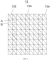
- FIG. 3 is a schematic structural diagram of a pixel unit in the display panel 10 shown in FIG. 2 .
- the display panel 10 includes pixel units 15 for display, and each pixel unit 15 corresponds to one pixel circuit 40.
- the pixel unit 15 includes multiple rows and multiple columns of sub-pixels. Each row includes a first sub-pixel 152, a second sub-pixel 154, and a third sub-pixel 156 which are sequentially arranged.
- Each column includes multiple sub-pixels of the same color, and each row of sub-pixels and each column of sub-pixels form a pixel array.
- the first sub-pixel 152 may be a red sub-pixel
- the second sub-pixel 154 may be a green sub-pixel
- the third sub-pixel 156 may be a blue sub-pixel.
- the first sub-pixel 152, the second sub-pixel 154, and the third sub-pixel 156 may not comply with the described correspondence in color, and they can be sub-pixels of other colors, which is not specifically limited in the disclosure.
- each sub-pixel includes a first light-emitting element A and a second light-emitting element B.
- each of the first sub-pixel 152, the second sub-pixel 154, and the third sub-pixel 156 includes the first light-emitting element A and the second light-emitting element B.
- both the first light-emitting element A and the second light-emitting element B may be organic light-emitting diodes (OLEDs), and thus the display panel 10 forms a dual-light OLED display.
- OLEDs organic light-emitting diodes
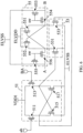
- FIG. 4 is a schematic diagram of a circuit structure of a pixel circuit 40 according to embodiments of the disclosure.
- the pixel circuit 40 includes a control unit 50, a light-emitting unit 60, and a drive unit 70.
- the light-emitting unit 60 includes the first light-emitting element A and the second light-emitting element B, and the first light-emitting element A and the second light-emitting element B are both electrically connected to the drive unit 70 and the control unit 50.
- the drive unit 70 is configured to transmit a data signal Data to the light-emitting unit 60, the data signal Data is used for driving the first light-emitting element A and/or the second light-emitting element B to emit light.
- the control unit 50 is configured to control the first light-emitting element A and/or the second light-emitting element B to be electrically connected to a first power supply ELVSS.
- the control unit 50 is configured to selectively control the first light-emitting element A and/or the second light-emitting element B to emit light.
- the color of light of the light-emitting unit 60 may be the color of the first sub-pixel 152, the second sub-pixel 154, or the third sub-pixel 156 correspondingly, which is not specifically limited in the disclosure.
- control unit 50 is further configured to control the first light-emitting element A or the second light-emitting element B to be electrically connected to a second power supply ELVDD, so that the first light-emitting element A releases (in other words, discharges) charges accumulated in the first light-emitting element A or the second light-emitting element B discharges charges accumulated in the second light-emitting element B.
- the first power supply ELVSS may be a low potential pixel power supply
- the second power supply ELVDD may be a high potential pixel power supply, which is not specifically limited in the disclosure.
- the drive unit 70 includes a data input end, a scan input end, and an output end.
- the data input end is electrically connected to the data line, and the drive unit 70 is configured to receive the data signal Data via the data line.
- the scan input end is electrically connected to the scan line, and the drive unit 70 is configured to receive a scan signal Scan via the scan line.
- the drive unit 70 is configured to selectively control, according to a received data signal Data and a received scan signal Scan , the power supply signal VDD to be transmitted from the output end to the light-emitting unit 60.
- the drive unit 70 may include a first transistor 71, a second transistor 73, and a storage capacitor 75.
- each of the first transistor 71 and the second transistor 73 includes a control end, a first end, and a second end.
- One end of the storage capacitor 75 is electrically connected to the second end of the first transistor 71, and the other end of the storage capacitor 75 is electrically connected to the first end of the second transistor 73.
- the storage capacitor 75 is configured to store image data which is used for controlling the light-emitting unit 60 to emit light.
- the control end of the first transistor 71 is electrically connected to the scan input end, and is configured to receive the scan signal Scan from the scan input end.
- the first end of the first transistor 71 is electrically connected to the data input end, and is configured to receive the data signal Data from the data input end.
- the second end of the first transistor 71 is electrically connected to the control end of the second transistor 73.
- the first transistor 71 is selectively electrically connected or disconnected according to a potential of the received scan signal Scan.
- the data signal Data is transmitted to the control end of the second transistor 73 from the second end of the first transistor 71.
- the first end of the second transistor 73 is configured to receive the power supply signal VDD, and the second end of the second transistor 73 is electrically connected to the output end.
- the second transistor 73 is selectively turned on or off according to the data signal Data received by the control end. In other words, the second transistor 73 is selectively electrically connected or disconnected according to the potential of the received data signal Data, so as to selectively transmit the power supply signal VDD to the output end.
- the first end of the second transistor 73 is electrically disconnected from the second end of the second transistor 73.
- the first end of the second transistor 73 is electrically connected to the second end of the second transistor 73.
- the power supply signal VDD is transmitted to the output end, and further, the power supply signal VDD is transmitted to the light-emitting unit 60 through the output end.
- the first potential may be a high potential
- the second potential may be a low potential, which is not specifically limited in the disclosure.
- the first transistor 71 and the second transistor 73 may be p-metal-oxide-semiconductor (PMOS) transistors, which is not specifically limited in the disclosure.
- the first end may be a drain electrode ("drain” for short)
- the second end may be a source electrode ("source” for short)
- the control end may be a gate electrode ("gate” for short).
- the light-emitting unit 60 may include the first light-emitting element A and the second light-emitting element B.
- the first end of the first light-emitting element A and the first end of the second light-emitting element B are both electrically connected to the output end, and the second end of the first light-emitting element A and the second end of the second light-emitting element B are both electrically connected to the control unit 50.
- the first end of the first light-emitting element A and the first end of the second light-emitting element B may be anodes, and the second end of the first light-emitting element A and the second end of the second light-emitting element B may be cathodes.
- control unit 50 is configured to receive a first signal ab and a second signal sw, and control, according to a potential of a received first signal ab and a potential of a received second signal sw, the second end of the first light-emitting element A and/or the second end of the second light-emitting element B to be electrically connected to the first power supply ELVSS, so as to selectively control the first light-emitting element A and/or the second light-emitting element B to emit light.
- the second end of the first light-emitting element A when the first signal ab received by the control unit 50 is at the first potential and the second signal sw is at the first potential, the second end of the first light-emitting element A is electrically connected to the first power supply ELVSS and receives a first cathode voltage from the first power supply ELVSS.
- the first light-emitting element A is configured to emit light.
- the second end of the second light-emitting element B is electrically connected to the first power supply ELVSS and receives the first cathode voltage from the first power supply ELVSS.
- the second light-emitting element B is configured to emit light.
- the second end of the first light-emitting element A and the second end of the second light-emitting element B are both electrically connected to the first power supply ELVSS, and simultaneously receive the first cathode voltage from the first power supply ELVSS, and in this case, both the first light-emitting element A and the second light-emitting element B emit light.
- control unit 50 may further control the second end of the first light-emitting element A or the second end of the second light-emitting element B to be electrically connected to the second power supply ELVDD and to receive a second cathode voltage from the second power supply ELVDD.
- an external electric field of the first light-emitting element A and/or the second light-emitting element B is in the same direction as an internal field formed by charges accumulated inside the first light-emitting element A and/or the second light-emitting element B, thus the charges accumulated inside the first light-emitting element A and/or the second light-emitting element B are thus depleted. In this way, the service life of the light-emitting unit 60 is prolonged, and the risk of screen burning is reduced.
- the second end of the second light-emitting element B is electrically connected to the second power supply ELVDD, and receives the second cathode voltage from the second power supply ELVDD.
- an external electric field of the second light-emitting element B is in the same direction as an internal electric field formed by the charges accumulated inside the second light-emitting element B, and the charges accumulated inside the second light-emitting element B are depleted, thereby prolonging the service life of the second light-emitting element B and reducing the risk of screen burning.
- the second end of the first light-emitting element A is electrically connected to the second power supply ELVDD, and receives the second cathode voltage from the second power supply ELVDD.
- an external electric field of the first light-emitting element A is in the same direction as an internal electric field formed by the charges accumulated inside the first light-emitting element A, and the charges accumulated inside the first light-emitting element A are depleted, thereby prolonging the service life of the first light-emitting element A and reducing the risk of screen burning.
- both the first light-emitting element A and the second light-emitting element B emit light to supplement the luminance of the light-emitting element, so as to avoid the problem of image sticking or screen burning caused by insufficient luminance, thereby improving the service life of the pixel circuit 40 and improving the display effect of the display panel 10.
- a potential of a second cathode voltage of the second power supply ELVDD is higher than a potential of the power supply signal VDD.
- a potential of a first cathode voltage of the first power supply ELVSS should be lower than the potential of the power supply signal VDD, so as to ensure that the light-emitting element emits light normally.
- the power supply signal VDD is used for driving the light-emitting element to emit light, and a voltage value of the power supply signal VDD should match the luminance of the light-emitting element, which is not specifically limited in the disclosure.
- a switching time for the second signal sw to switch from the first potential to the second potential or from the second potential to the first potential can also be determined according to practical situations, which is not specifically limited in the disclosure.
- the first light-emitting element A emits light: the drive unit 70 receives the scan signal Scan at the second potential and the data signal Data at the second potential, thus the first transistor 71 and the second transistor 73 are in an ON-state, that is, turned on.
- the power supply signal VDD is output from the output end to the light-emitting unit 60, and both the first end of the first light-emitting element A and the first end of the second light-emitting element B receive the power supply signal.
- the control unit 50 receives the first signal ab at the first potential and the second signal sw at the first potential, such that the second end of the first light-emitting element A is electrically connected to the first power supply ELVSS to receive the first cathode voltage, and the second end of the second light-emitting element B is electrically connected to the second power supply ELVDD to receive the second cathode voltage.
- the first light-emitting element A emits light
- the second light-emitting element B discharges charges accumulated in the second light-emitting element B.
- the second light-emitting element B emits light: the drive unit 70 receives the scan signal Scan at the second potential and the data signal Data at the second potential, thus the first transistor 71 and the second transistor 73 are in the ON-state.
- the power supply signal is output from the output end to the light-emitting unit 60, and both the first end of the first light-emitting element A and the first end of the second light-emitting element B receive the power supply signal.
- the control unit 50 receives the first signal ab at the second potential and the second signal sw at the first potential, such that the second end of the second light-emitting element B is electrically connected to the first power supply ELVSS to receive the first cathode voltage, and the second end of the first light-emitting element A is electrically connected to the second power supply ELVDD to receive the second cathode voltage.
- the second light-emitting element B emits light
- the first light-emitting element A discharges charges accumulated in the first light-emitting element A.
- the first light-emitting element A and the second light-emitting element B both emit light: the drive unit 70 receives the scan signal Scan at the second potential and the data signal Data at the second potential, thus the first transistor 71 and the second transistor 73 are in an ON-state.
- the power supply signal is output from the output end to the light-emitting unit 60, and both the first end of the first light-emitting element A and the first end of the second light-emitting element B receive the power supply signal.
- the control unit 50 receives the second signal sw at the second potential, so that the second end of the first light-emitting element A and the second end of the second light-emitting element B are both electrically connected to the first power supply ELVSS to receive the first cathode voltage. In this case, both the first light-emitting element A and the second light-emitting element B emit light.
- the control unit 50 includes a conduction selection unit 51, a conduction control unit 53, and a switch unit 55.
- the conduction control unit 53 is electrically connected to both the conduction selection unit 51 and the switch unit 55, and the switch unit is further electrically connected to the first light-emitting element and the second light-emitting element.
- the conduction selection unit 51 is configured to receive a power supply control signal VDD1 and the first signal ab, and selectively control, according to the first signal ab, the conduction control unit 53 to be in a first conductive state or a second conductive state.
- the switch unit 55 receives the second signal sw, and the switch unit 55 controls, according to a conductive state of the conduction selection unit 51 and a potential of the second signal sw, the second end of the first light-emitting element and/or the second end of the second light-emitting element to be electrically connected to the first power source. Specifically, the switch unit 55 controls the second end of the first light-emitting element A to be electrically connected to the first power supply ELVSS, and the second end of the second light-emitting element B to be electrically connected to the second power supply ELVDD.
- the switch unit 55 drives the second end of the second light-emitting element B to be electrically connected to the first power supply ELVSS, and drives the second end of the first light-emitting element A to be electrically connected to the second power supply ELVDD.
- the second end of the first light-emitting element A and the second end of the second light-emitting element B are both electrically connected to the first power supply ELVSS.
- the conduction selection unit 51 includes a first selection transistor 511, a second selection transistor 513, a third selection transistor 515, and a fourth selection transistor 517.
- a control end of the first selection transistor 511 is configured to receive the first signal ab
- a control end of the second selection transistor 513 is configured to receive an inverted signal BA of the first signal ab.
- a first end of the first selection transistor 511 and a first end of the second selection transistor 513 are configured to receive the power supply control signal VDD1, and a second end of the first selection transistor 511 is electrically connected to both a first end of the third selection transistor 515 and the conduction control unit 53.
- a second end of the second selection transistor 513 is electrically connected to a first end of the fourth selection transistor 517 and the conduction control unit 53.
- the inverted signal BA of the first signal ab is NOT-a and NOT-b.
- a control end of the third selection transistor 515 is electrically connected to the second end of the second selection transistor 513.
- a control end of the fourth selection transistor 517 is electrically connected to the second end of the first selection transistor 511.
- a second end of the third selection transistor 515 and a second end of the fourth selection transistor 517 are both electrically connected to the first power supply ELVSS.
- control end of the first selection transistor 511 is configured to receive the first signal ab, and the first signal ab is used for controlling the first end of the first selection transistor 511 to be electrically connected to or electrically disconnected from the second end of the first selection transistor 511.
- control end of the fourth selection transistor 517 is configured to receive the power supply control signal VDD1 from the second end of the first selection transistor 511, and the power supply control signal VDD1 is used for controlling the first selection transistor 511 to be in an ON-state or an OFF-state, that is, turned on or turned off. Meanwhile, the power supply control signal VDD1 is selectively transmitted to the conduction control unit 53 from the second end of the first selection transistor 511.
- the first end of the first selection transistor 511 When the first signal ab is at the first potential, the first end of the first selection transistor 511 is electrically disconnected from the second end of the first selection transistor 511, and the power supply control signal VDD1 cannot be transmitted from the first end to the second end. In this case, the control end of the fourth selection transistor 517 fails to receive the power supply control signal VDD1, and is in an OFF-state. The power supply control signal VDD1 cannot be transmitted to the conduction control unit 53 from the second end of the first selection transistor 511.
- the first end of the first selection transistor 511 is electrically connected to the second end of the first selection transistor 511, and the power supply control signal VDD1 is transmitted from the first end to the second end.
- the control end of the fourth selection transistor 517 receives the power supply control signal VDD1, and is in an ON-state.
- the power supply control signal VDD1 is transmitted to the conduction control unit 53 from the second end of the first selection transistor 511.
- control end of the second selection transistor 513 is configured to receive the inverted signal BA of the first signal ab, and the inverted signal BA is used for controlling the first end of the second selection transistor 513 and the second end of the second selection transistor 513 to be electrically connected to or electrically disconnected from each other.
- control end of the third selection transistor 515 is configured to receive the power supply control signal VDD1 from the second end of the second selection transistor 513, and the power supply control signal VDD1 is used for controlling the third selection transistor 515 to be in an ON-state or an OFF-state. Meanwhile, the power supply control signal VDD1 is selectively transmitted to the conduction control unit 53 from the second end of the second selection transistor 513.
- the control end of the third selection transistor 515 does not receive the power supply control signal VDD1, and is in an OFF-state.
- the power supply control signal VDD1 cannot be transmitted to the conduction control unit 53 from the second end of the second selection transistor 513.
- the first end of the second selection transistor 513 and the second end of the second selection transistor 513 are electrically connected, and the power supply control signal VDD1 is transmitted from the first end of the second selection transistor 513 to the second end of the second selection transistor 513.
- the control end of the third selection transistor 515 receives the power supply control signal VDD1, and is in an ON-state.
- the power supply control signal VDD1 is transmitted to the conduction control unit 53 from the second end of the second selection transistor 513.
- the conduction control unit 53 includes a first conductive transistor 531 and a second conductive transistor 533.
- a control end of the first conductive transistor 531 is electrically connected to the second end of the second selection transistor 513, and a control end of the second conductive transistor 533 is electrically connected to the second end of the first selection transistor 511.
- a first end of the first conductive transistor 531 and a first end of the second conductive transistor 533 are both electrically connected to the first power supply ELVSS.
- a second end of the first conductive transistor 531 and a second end of the second conductive transistor 533 are both electrically connected to the switch unit 55.
- control end of the first conductive transistor 531 is configured to receive the power supply control signal VDD1 from the second end of the second selection transistor 513, and the power supply control signal VDD1 is used for controlling the first conductive transistor 531 to be in an ON-state or an OFF-state.
- the control end of the second conductive transistor 533 is configured to receive the power supply control signal VDD1 from the second end of the first selection transistor 511, and the power supply control signal VDD1 is used for controlling the second conductive transistor 533 to be in an ON-state or an OFF-state.
- the power supply control signal VDD1 is always at the first potential
- the first conductive transistor 531 or the second conductive transistor 533 receives the power supply control signal VDD1
- the first conductive transistor 531 or the second conductive transistor 533 is turned on.
- the second end of the first conductive transistor 531 or the second end of the second conductive transistor 533 is electrically connected to the first power supply ELVSS.
- the control end of the first conductive transistor 531 receives the power supply control signal VDD1 from the second end of the second selection transistor 513, the first conductive transistor 531 is in an ON-state, and the second conductive transistor 533 is in an OFF-state. In this case, the conduction control unit 53 is in the first conductive state.
- the control end of the second conductive transistor 533 When the control end of the second conductive transistor 533 receives the power supply control signal VDD1 from the second end of the first selection transistor 511, the first conductive transistor 531 is in an OFF-state, and the second conductive transistor 533 is in an ON-state. In this case, the conduction control unit 53 is in the second conductive state.
- the switch unit 55 includes a first discharge transistor 551, a second discharge transistor 552, a third discharge transistor 554, and a fourth discharge transistor 556.
- a control end of the first discharge transistor 551 is electrically connected to the second end of the first conductive transistor 531, and a control end of the second discharge transistor 552 is electrically connected to the second end of the second conductive transistor 533.
- a first end of the first discharge transistor 551 and a first end of the second discharge transistor 552 are both electrically connected to the second power supply ELVDD.
- a second end of the first discharge transistor 551 is electrically connected to a second end of the second conductive transistor 533, and a second end of the second discharge transistor 552 is electrically connected to a second end of the first conductive transistor 531.
- a control end of the third discharge transistor 554 is configured to receive the second signal sw.
- a first end of the third discharge transistor 554 is electrically connected to both the second end of the second conductive transistor 533 and the second end of the first discharge transistor 551.
- a second end of the third discharge transistor 554 is electrically connected to the second end of the second light-emitting element B.
- a control end of the fourth discharge transistor 556 is configured to receive the second signal sw, and a first end of the fourth discharge transistor 556 is electrically connected to both the second end of the first conductive transistor 531 and the second end of the second discharge transistor 552. A second end of the fourth discharge transistor 556 is electrically connected to the second end of the first light-emitting element A.
- control end of the first discharge transistor 551 is configured to receive the first cathode voltage of the first power supply ELVSS from the second end of the first conductive transistor 531, and the first cathode voltage of the first power supply ELVSS is used for controlling the first end of the first discharge transistor 551 and the second end of the first discharge transistor 551 to be electrically connected.
- the control end of the second discharge transistor 552 is configured to receive a first cathode voltage of the first power supply ELVSS from the second end of the second conductive transistor 533, and the first cathode voltage of the first power supply ELVSS is used for controlling the first end of the second discharge transistor 552 and the second end of the second discharge transistor 552 to be electrically connected.
- the first cathode voltage is always at the second potential
- the control end of the first discharge transistor 551 receives the first cathode voltage
- the first discharge transistor 551 is in an ON-state
- the second cathode voltage of the second power supply ELVDD is transmitted to the second end of the first discharge transistor 551 from the first end of the first discharge transistor 551; or when the control end of the second discharge transistor 552 receives the first cathode voltage, the second discharge transistor 552 is in an ON-state, and the second cathode voltage of the second power supply ELVDD is transmitted to the second end of the second discharge transistor 552 from the first end of the second discharge transistor 552.
- control end of the third discharge transistor 554 receives the second signal sw, and the second signal sw is used for controlling the third discharge transistor 554 to be in an ON-State or OFF-state.
- the third discharge transistor 554 when the second signal sw is at the first potential, the third discharge transistor 554 is turned on, and when the second signal sw is at the second potential, the third discharge transistor 554 is turned off.
- control end of the fourth discharge transistor 556 receives the second signal sw, and the second signal sw is used for controlling the fourth discharge transistor 556 to be in an ON-State or OFF-state.
- the fourth discharge transistor 556 when the second signal sw is at the first potential, the fourth discharge transistor 556 is in the ON-state. When the second signal sw is at the second potential, the fourth discharge transistor 556 is in an OFF-state. Accordingly, when the third discharge transistor 554 is in the ON-state and the conduction control unit 53 is in the first conductive state, the first light-emitting element A emits light. When the fourth discharge transistor 556 is in the ON-state and the conduction control unit 53 is in the second conductive state, the second light-emitting element B emits light.
- the switch unit 55 further includes a first switch transistor 555 and a second switch transistor 553.
- a control end of the first switch transistor 555 and a control end of the second switch transistor 553 are configured to receive the second signal sw, and a first end of the first switch transistor 555 and a first end of the second switch transistor 553 are both electrically connected to the first power supply ELVSS.
- a second end of the first switch transistor 555 is electrically connected to the second end of the first light-emitting element A, and a second end of the second switch transistor 553 is electrically connected to the second end of the second light-emitting element B.
- the second signal sw is used for controlling the first switch transistor 555 and the second switch transistor 553 to be in an ON-state or OFF-state.
- both the first light-emitting element A and the second light-emitting element B emit light to supplement the luminance of the light-emitting elements, so as to avoid the problem of image sticking or screen burning due to insufficient luminance, thereby improving the service life of the pixel circuit 40 and improving the display effect of the display panel 10.
- the first switch transistor 555 and the second switch transistor 553 are both turned off. Signal inputs at the second end of the first light-emitting element A and the second end of the second light-emitting element B are controlled by the first discharge transistor 551, the second discharge transistor 552, the third discharge transistor 554, and the fourth discharge transistor 556.
- the second discharge transistor 552 when the conduction control unit 53 is in the first conductive state and the second signal sw is at the first potential, the first discharge transistor 551, the third discharge transistor 554, and the fourth discharge transistor 556 are turned on, the second discharge transistor 552 is turned off.
- the first cathode voltage of the first power supply ELVSS is transmitted to the second end of the first light-emitting element A, the first light-emitting element A emits light
- the second cathode voltage of the second power supply ELVDD is transmitted to the second end of the second light-emitting element B.
- the conduction control unit 53 When the conduction control unit 53 is in the second conductive state and the second signal sw is at the first potential, the second discharge transistor 552, the third discharge transistor 554, and the fourth discharge transistor 556 are turned on, the first discharge transistor 551 is turned off.
- the first cathode voltage of the first power supply ELVSS is transmitted to the second end of the second light-emitting element B, the second light-emitting element B emits light
- the second cathode voltage of the second power supply ELVDD is transmitted to the second end of the first light-emitting element A.
- both the first switch transistor 555 and the second switch transistor 553 are turned on, and the first cathode voltage of the first power supply ELVSS is transmitted to the second end of the first light-emitting element A and the second end of the second light-emitting element B respectively.
- the first selection transistor 511, the second selection transistor 513, the third selection transistor 515, the fourth selection transistor 517, the first conductive transistor 531, the second conductive transistor 533, the first discharge transistor 551, the second discharge transistor 552, the first switch transistor 555, the third discharge transistor 554, the second switch transistor 553, and the fourth discharge transistor 556 can be metal-oxide-semiconductor field-effect transistors (MOSFETs), which are not specifically limited in the disclosure.
- the third selection transistor 515, the fourth selection transistor 517, the first conductive transistor 531, the second conductive transistor 533, the third discharge transistor 554, and the fourth discharge transistor 556 may be N-channel MOS field effect transistors.
- the first selection transistor 511, the second selection transistor 513, the first discharge transistor 551, the second discharge transistor 552, the first switch transistor 555 and the second switch transistor 553 may be P-channel MOS field effect transistors, which is not specifically limited in the disclosure.
- the first ends thereof can each be a drain, the second ends thereof can each be a source, and the control ends thereof can each be a gate.
- the first ends thereof can each be a source, the second ends thereof can each be a drain, and the control ends thereof can each be a gate.
- control unit 50 controls the first light-emitting element A and/or the second light-emitting element B to emit light.
- the first light-emitting element A is configured to emit light: when the first signal ab is at the first potential and the second signal sw is at the first potential, the first selection transistor 511 is turned off, and the second selection transistor 513 is turned on. Therefore, the fourth selection transistor 517 is turned off, and the power supply control signal VDD1 is transmitted to the second end of the second selection transistor 513 from the first end of the second selection transistor 513.
- the control end of the third selection transistor 515 and the control end of the first conductive transistor 531 receive the power supply control signal VDD1 from the second end of the second selection transistor 513, and the third selection transistor 515 and the first conductive transistor 531 are turned on. Thus, the first cathode voltage of the first power supply ELVSS is transmitted to the second end of the first conductive transistor 531.
- the fourth discharge transistor 556 Since the control end of the fourth discharge transistor 556 receives the second signal sw at the first potential and the fourth discharge transistor 556 is turned on, the first cathode voltage is transmitted from the second end of the first conductive transistor 531 to the second end of the fourth discharge transistor 556, and further to the second end of the first light-emitting element A. Further, the first light-emitting element A is configured to emit light.
- the control end of the first discharge transistor 551 receives the first cathode voltage from the second end of the first conductive transistor 531, and the first discharge transistor 551 is turned on, and then the second cathode voltage of the second power supply ELVDD is transmitted to the second end of the first discharge transistor 551 from the first end of the first discharge transistor 551. Since the control end of the third discharge transistor 554 receives the second signal sw which is at the first potential and the third discharge transistor 554 is turned on, the second cathode voltage is further transmitted to the second end of the second light-emitting element B via the third discharge transistor 554. In this case, the second light-emitting element B does not emit light, and charges accumulated in the second light-emitting element B are discharged, thereby avoiding display image sticking and prolonging the service life.
- the second light-emitting element B is configured to emit light: when the first signal ab is at the second potential and the second signal sw is at the first potential, the first selection transistor 511 is turned on, and the second selection transistor 513 is turned off. Therefore, the third selection transistor 515 is turned off, and the power supply control signal VDD1 is transmitted from the first end of the first selection transistor 511 to the second end of the first selection transistor 511.
- the control end of the fourth selection transistor 517 and the control end of the second conductive transistor 533 receive the power supply control signal VDD1 from the second end of the first selection transistor 511, and the fourth selection transistor 517 and the second conductive transistor 533 are turned on. Thus, the first cathode voltage of the first power supply ELVSS is supplied to the second end of the second conductive transistor 533.
- the control end of the third discharge transistor 554 receives the second signal sw which is at the first potential and the third discharge transistor 554 is turned on, the first cathode voltage is transmitted from the second end of the second conductive transistor 533 to the second end of the third discharge transistor 554 and further to the second end of the second light-emitting element B. In this case, the second light-emitting element B emits light.
- Both the first light-emitting element A and the second light-emitting element B are configured to emit light: when the second signal sw is at the second potential, the first switch transistor 555 and the second switch transistor 553 are both turned on, the second end of the first switch transistor 555 and the second end of the second switch transistor 553 are both electrically connected to the first power supply ELVSS, and the second end of the first light-emitting element A and the second end of the second light-emitting element B are both electrically connected to the first power supply ELVSS.
- the first light-emitting element A and the second light-emitting element B emit light at the same time to supplement the luminance of the light-emitting elements, so as to avoid the problem of image sticking or screen burning caused by insufficient luminance, thereby improving the service life of the pixel circuit 40 and improving the display effect of the display panel 10.
- FIG. 7 is an operation timing diagram of the pixel circuit 40 shown in FIG. 5 .
- the curves corresponding to Scan n and Scan n+1 respectively correspond to any two adjacent timing in the data line
- a curve corresponding to Data is a timing corresponding to the data signal Data
- a curve corresponding to ab is a timing corresponding to the first signal ab
- a curve corresponding to sw is a timing corresponding to the second signal sw.
- a potential switching of the first signal ab corresponds to a preset switching time, that is, the potential of the first signal ab is switched once every time the preset switching time elapses.
- the preset switching time may be 200 frames. It should be understood that, the preset switching time may be determined according to a specific condition of the display device 100, which is not specifically limited in the disclosure.
- the pixel circuit 40 is provided with a control unit 50
- the light-emitting unit 60 is provided with the first light-emitting element A and the second light-emitting element B
- the control unit 50 is configured to selectively control the first light-emitting element A and/or the second light-emitting element B to emit light, so as to prolong the service life of the pixel circuit 40.
- control unit 50 is configured to selectively control the first light-emitting element A or the second light-emitting element B to be electrically connected to the second power supply ELVDD so as to receive the second cathode voltage, thereby discharging the charges accumulated in the light-emitting element when the light-emitting element does not emit light, and further improving the service life of the light-emitting unit 60, reducing the risk of screen burning, and improving the display quality.
- the disclosure further provides a display panel 10, and the display panel 10 includes multiple pixel circuits 40 as described above.
- FIG. 8 is a schematic diagram of another display panel 1 according to embodiments of the disclosure.
- the difference between the display panel 1 and the display panel 10 lies in that the display panel 1 further includes a general control unit 18.
- the general control unit 18 is electrically connected to multiple pixel circuits 40, and the general control unit 18 is configured to simultaneously control multiple pixel circuits 40 to switch to a first light-emitting element A and/or a second light-emitting element B, to make the first light-emitting element A and/or the second light-emitting element B emit light.
- the display block includes nine pixel circuits 40. It can be understood that, the pixel circuits 40 in the display panel 1 are controlled in blocks, and the number of the pixel circuits included in each display block may be determined according to actual situations, which is not specifically limited in the disclosure.
- communication may be implemented between the general control unit 18 and the pixel circuit 40 by an inter-integrated circuit bus (IIC), a serial peripheral interface (SPI), or the like, and how to select a protocol may be determined according to actual situations, which is not specifically limited in the disclosure.
- IIC inter-integrated circuit bus
- SPI serial peripheral interface
- the display panel 10 includes multiple pixel circuits 40, each of the pixel circuits 40 includes one control unit 50, each control unit 50 corresponds to one address, and the general control unit 18 is configured to transmit control signals to the multiple control units 50.
- the control signal includes a start segment, multiple address segments, and multiple instruction segments, where the start segment includes a 0.5 milliseconds (ms) start signal at a first potential, each address segment is a 4 microsecond ( ⁇ s) data signal containing a block address, and each instruction segment is a 2 ⁇ s data signal containing instruction information.
- control signal includes a start part and multiple data parts, the start part does not include data information, and each data part includes data of six bytes (bits), where the first four bits are addresses of corresponding display blocks, and the last two bits are corresponding signal instructions.
- the signal instruction corresponds to a second signal sw and a first signal ab.
- the display blocks controlled by the general control unit 18 receive the control signal, and the address segment of the control signal identifies the corresponding control unit and then continues to output the instruction segment of the control signal, so as to control the pixel circuit 40 to switch the light-emitting element for emitting light. It can be understood that the pixel circuit 40 which does not correspond to the address segment of the control signal continues to make the light-emitting element, which is originally configured to emit light, emit light.
- 1 bit corresponds to 1 ⁇ s, which is not specifically limited in the disclosure, and the length of the signal included in the control signal can be determined according to actual situations.
- FIG. 9 is a timing diagram of the control signal sent by the general control unit 18 in the display panel 1 shown in FIG. 8 .
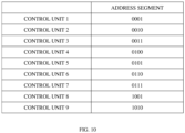
- FIG. 10 shows addresses corresponding to each control unit in the display panel 1 shown in FIG. 8 .
- the timing diagram of the control signal sent by the general control unit 18 is shown in FIG. 9 , where a start segment of the control signal is "111111", and a first address segment is 0001.
- the first instruction segment is 11, where the first 1 of the first instruction segment corresponds to the first signal ab at the first potential, and the second 1 of the first instruction segment corresponds to the second signal sw at the first potential.
- the second address segment is 0010, and a second instruction segment is also 11, where the first 1 of the second instruction segment corresponds to the first signal ab at the first potential, and the second 1 of the second instruction segment corresponds to the second signal sw at the first potential.
- the third address segment is 0011, and the third instruction segment is 01, where 0 of the third instruction segment corresponds to the first signal ab at a second potential, and 1 of the third instruction segment corresponds to the second signal sw at the first potential.
- Different control units 50 according to the address segment of the control signal received, correspondingly receive or not receive the instruction segment. Specifically, the general control unit 18 transmits the instruction signal corresponding to the address segment to the control unit 50 corresponding to the address segment, so as to control the pixel circuit 40 to switch the light-emitting element for emitting light.
- control units 50 of nine pixel circuits 40 shown in FIG. 8 are sequentially marked as control unit 1, control unit 2, to control unit 9, and addresses corresponding to the nine control units 50 are shown in the figure.
- each block includes nine pixel circuits.
- the general control unit 18 is electrically connected to the control units 50 of the nine pixel circuits 40.
- the general control unit 18 may control the two or more pixel circuits 40 to switch the light-emitting element of the light-emitting unit 60 to make the light-emitting element emit light.
- the display abnormality refers to phenomena such as screen burning, image sticking, or the like.
- the general control unit simultaneously controls two pixel circuits 40 to switch the light-emitting element
- two of the pixel circuits in the display block are denoted as a first pixel circuit and a second pixel circuit.
- the general control unit 18 when the first light-emitting element A of the first pixel circuit is abnormal and the second light-emitting element B of the second pixel circuit is abnormal, the general control unit 18 simultaneously controls the first pixel circuit and the second pixel circuit to switch to the other light-emitting element for displaying a picture. Specifically, the first pixel circuit is switched to the second light-emitting element B for display, and the second pixel circuit is switched to the first light-emitting element A for display. It can be understood that the general control unit 18 may also control three, four, or other number of pixel circuits 40 to switch the light emitting elements at the same time, which is not specifically limited in the disclosure.
- the disclosure further provides a display device 100, which includes the described display panel.
- the pixel circuit 40 is provided with the control unit 50
- the light-emitting unit 60 is provided with the first light-emitting element A and the second light-emitting element B
- the control unit 50 is configured to selectively control the first light-emitting element A and/or the second light-emitting element B to emit light, so as to improve the service life of the pixel circuit 40.
- control unit 50 is configured to selectively control the first light-emitting element A or the second light-emitting element B to be electrically connected to the second power supply ELVDD to receive the second cathode voltage, and the first light-emitting element discharges charges accumulated in the first light-emitting element when the first light-emitting element does not emit light, or the second light-emitting element discharges charges accumulated in the second light-emitting element when the second light-emitting element does not emit light, thus further improving the service life of the light-emitting unit 60, reducing the risk of screen burning, and improving the display quality.
- the display panel is provided with the general control unit 18 to control multiple pixel circuits 40 in the display panel based on blocks.
- Each display block is provided with the general control unit 18, and the general control unit 18 is configured to switch pixel circuits 40 with display abnormality to the light-emitting element for displaying, thereby further improving the efficiency of controlling the display effect.
Landscapes
- Engineering & Computer Science (AREA)
- Physics & Mathematics (AREA)
- Computer Hardware Design (AREA)
- General Physics & Mathematics (AREA)
- Theoretical Computer Science (AREA)
- Control Of Indicators Other Than Cathode Ray Tubes (AREA)
- Electroluminescent Light Sources (AREA)
- Control Of El Displays (AREA)
Abstract
Description
- This application claims priority to and the benefit of
Chinese Patent Application No. 202211145865.8, filed September 20, 2022 - This disclosure relates to the field of display technology, and particularly relates to a pixel circuit, a display panel having the pixel circuit, and a display device having the display panel.
- With the development of display technology, market demands for display effect and quality of display devices are gradually increasing. In the market, an Organic Light-Emitting Diode (OLED) display screen generally adopts a direct-current driving mode. However, in the direct current driving mode, the OLED accumulates residual un-recombined carriers at an interface between a hole transport layer and a light-emitting layer or at an interface between the light-emitting layer and an electron transport layer. After the residual un-recombined carriers accumulate to a certain degree, a built-in electric field (also known as internal electric field) is formed inside. However, the formed built-in electric field may cause difficulty in injection of carriers in the next cycle, and further cause reduction of the recombination rate, thereby affecting the display quality and the service life of the OLED display screen.
- The present disclosure aims to provide a pixel circuit, a display panel, and a display device. The pixel circuit is provided with a first light-emitting element and a second light-emitting element. The control unit is configured to selectively control the first light-emitting element and/or the second light-emitting element to emit light. Meanwhile, the control unit is configured to control the first light-emitting element or the second light-emitting element to receive a second cathode voltage, and the first light-emitting element discharges charges accumulated in the first light-emitting element when the first light-emitting element does not emit light, or the second light-emitting element discharges charges accumulated in the second light-emitting element when the second light-emitting element does not emit light, so as to prolong the service life of the light-emitting unit, reduce the risk of screen burning, and improve the display quality of the screen.
- In a first aspect of the disclosure, a pixel circuit is provided. The pixel circuit includes a light-emitting unit, a drive unit, and a control unit, where the light-emitting unit includes a first light-emitting element and a second light-emitting element, and the first light-emitting element and the second light-emitting element are electrically connected to the drive unit and the control unit; the drive unit is configured to transmit to the light-emitting unit a data signal for driving the first light-emitting element and/or the second light-emitting element to emit light. The control unit is configured to control the first light-emitting element and/or the second light-emitting element to be electrically connected to a first power supply, where the control unit is configured to selectively control the first light-emitting element and/or the second light-emitting element to emit light when the light-emitting unit receives the data signal.
- In a second aspect of the disclosure, a display panel is provided. The display panel includes several pixel circuits described above.
- In a third aspect of the disclosure, a display device is provided. The display device includes the display panel described above.
- In conclusion, for a pixel circuit, a display panel, and a display device provided in the present disclosure, the pixel circuit is provided with a control unit. A light-emitting unit is provided with a first light-emitting element and a second light-emitting element. The control unit is configured to selectively control the first light-emitting element and/or the second light-emitting element to selectively emit light to prolong the service life of the pixel circuit. Meanwhile, the control unit is configured to selectively control a second end of the first light-emitting element or a second end of the second light-emitting element to be electrically connected to a second power supply to receive a second cathode voltage, and the first light-emitting element discharges charges accumulated in the first light-emitting element when the first light-emitting element does not emit light or the second light-emitting element discharges charges accumulated in the second light-emitting element when the second light-emitting element does not emit light, so as to prolong the service life of the light-emitting unit, reduce the risk of screen burning, and improve the display quality of the screen.
- In addition, the display panel is provided with a general control unit to control multiple pixel circuits in the display panel based on blocks. Each display block is provided with the general control unit, and the general control unit is configured to switch pixel circuits with display abnormality to the light-emitting element for displaying, further improving the efficiency of controlling the display effect.
- In order to describe technical solutions in embodiments of the disclosure or the related art more clearly, the following will give a brief introduction to the accompanying drawings required for describing embodiments or the related art. Apparently, the accompanying drawings hereinafter described are merely some embodiments of the disclosure. Based on these drawings, those of ordinary skill in the art can also obtain other drawings without creative effort.
-
FIG. 1 is a schematic structural diagram of a display device disclosed in embodiments of the disclosure. -
FIG. 2 is a schematic structural diagram of a display panel in the display device shown inFIG. 1 . -
FIG. 3 is a schematic structural diagram of a pixel unit in the display panel shown inFIG. 2 . -
FIG. 4 is a schematic diagram of a circuit structure of a pixel circuit disclosed in embodiments of the disclosure. -
FIG. 5 is a schematic diagram of a specific circuit structure of the pixel circuit shown inFIG. 4 . -
FIG. 6 is a schematic diagram of a circuit structure of a control unit in the pixel circuit shown inFIG. 5 . -
FIG. 7 is an operation timing diagram of the pixel circuit shown inFIG. 5 . -
FIG. 8 is a schematic diagram of another display panel disclosed in embodiments of the disclosure. -
FIG. 9 is a timing diagram of control signals sent by a general control unit in the display panel shown inFIG. 8 . -
FIG. 10 shows addresses corresponding to each control unit in the display panel shown inFIG. 8 . - In order to facilitate understanding of the disclosure, the disclosure will be described more fully hereinafter with reference to the accompanying drawings. Preferred embodiments of the disclosure are shown in the drawings, but the disclosure may be implemented in many different forms and is not limited to the embodiments described herein. Rather, these embodiments are provided so that this disclosure will be thorough and complete.
- The following description of the embodiments refers to the accompanying drawings to illustrate specific embodiments of the disclosure. Sequential references themselves, such as "first", "second", etc., are used merely to distinguish between described objects and do not have any ordinal or technical meaning. However, the expressions "connected" and "coupled" in the disclosure, unless otherwise specified, both include direct connection and indirect connection. Directional terms mentioned in the disclosure, for example, "upper", "lower", "front", "rear", "left", "right", "inner", "outer", "side" and the like are only directions with reference to the accompanying drawings, and therefore, the directional terms are used for better and clearer illustration and understanding of the disclosure, rather than indicate or imply that the indicated device or element must have a particular orientation, be constructed and operated in a particular orientation, therefore, it cannot be understood that the disclosure is limited thereto.
- In the description of the disclosure, it should be noted that, unless specified or limited otherwise, the terms "mounted", "connected with", and "connected to" should be understood broadly, for example, may be fixedly connected, may also be detachably connected, or may be integrally connected; may also be mechanical connections; may also be direct connections or indirect connections via intervening structures; and may also be inner communications of two elements. The specific meanings of the above terms in the disclosure can be understood by those skilled in the art according to specific situations. It should be noted that terms such as "first" and "second" in the description and claims and drawings of the disclosure are used for distinguishing different objects, rather than for describing a specific sequence.
- In addition, as used herein, the term "include", "may include", "contain" or "may contain" indicates the existence of a corresponding disclosed function, operation, element, etc., and does not exclude one or more other functions, operations, elements, etc. In addition, the terms "comprise" or "include" means that there are corresponding features, numbers, steps, operations, elements, components, or a combination thereof disclosed in the specification, and do not exclude the presence or addition of one or more other features, numbers, steps, operations, elements, components, or a combination thereof, and are intended to cover a non-exclusive inclusion.
- It should also be understood that the meaning of "at least one" described herein is one and more than one, e. g., one, two, or three, etc., and the meaning of "a plurality of" or "multiple" is at least two, e. g., two or three, etc., unless specifically defined otherwise. The terms "
step 1", "step 2", and the like in the description and claims of the disclosure and the drawings are used for distinguishing different objects, rather than for describing a specific order. - Reference is made to
FIG. 1 , which is a schematic structural diagram of adisplay device 100 according to embodiments of the disclosure. As shown inFIG. 1 , thedisplay device 100 provided in embodiments of the disclosure may at least include adisplay panel 10, apower supply module 20, and asupport frame 30. Thedisplay panel 10 is fixed to thesupport frame 30, and thepower supply module 20 is arranged on a back side of thedisplay panel 10, that is, a non-display surface of thedisplay panel 10 or a side of thedisplay panel 10 facing away from a user. Thedisplay panel 10 is configured to display an image(s). Thepower supply module 20 is electrically connected to thedisplay panel 10 and is configured to provide a power supply voltage for thedisplay panel 10 to display an image. Thesupport frame 30 supports and protects thedisplay panel 10 and thepower supply module 20. - It can be understood that, the
display panel 10 further has a display surface which is opposite to the non-display surface, that is, a front side of thedisplay panel 10 or a side of thedisplay panel 10 facing the user. The display surface is configured to face the user who uses thedisplay device 100 to display an image. - Reference is made to
FIG. 2 , which is a schematic structural diagram showing adisplay panel 10 of thedisplay device 100 shown inFIG. 1 . As shown inFIG. 2 , thedisplay panel 10 includes adisplay area 11 and anon-display area 13. Thedisplay area 11 is configured to display the image, and thenon-display area 13 is disposed around thedisplay area 11 and is not used for image display. It should be understood that, in some embodiments, thedisplay panel 10 may use a liquid crystal material as a display medium, which is not limited thereto. - In embodiments of the disclosure, multiple scan lines extending along a first direction F1 and multiple data lines extending along a second direction F2 are provided within the
display panel 10 in a grid-like manner. The first direction F1 is perpendicular to the second direction F2 (seeFIG. 5 ), and the multiple scan lines, the multiple data lines, and the scan lines and the data lines are insulated from one another. In other words, the multiple scan lines are arranged at intervals along the second direction F2 and insulated from one another, the multiple data lines are arranged at intervals along the first direction F1 and insulated from one another, and the multiple scan lines and the multiple data lines are insulated from one another. - A
pixel circuit 40 is disposed at each of intersections of the multiple scan lines and the multiple data lines (seeFIG. 4 ). Specifically, thepixel circuit 40 is disposed between any two adjacent scan lines and any two adjacent data lines. Thepixel circuits 40 in the same column are all electrically connected to the same data line, and thepixel circuits 40 in the same row are all electrically connected to the same scan line. In embodiments of the disclosure, themultiple pixel circuits 40 are arranged in an array. - Reference is made to
FIG. 3 , which is a schematic structural diagram of a pixel unit in thedisplay panel 10 shown inFIG. 2 . As shown inFIG. 3 , thedisplay panel 10 includespixel units 15 for display, and eachpixel unit 15 corresponds to onepixel circuit 40. Thepixel unit 15 includes multiple rows and multiple columns of sub-pixels. Each row includes afirst sub-pixel 152, asecond sub-pixel 154, and athird sub-pixel 156 which are sequentially arranged. Each column includes multiple sub-pixels of the same color, and each row of sub-pixels and each column of sub-pixels form a pixel array. - In embodiments of the disclosure, the
first sub-pixel 152 may be a red sub-pixel, thesecond sub-pixel 154 may be a green sub-pixel, and thethird sub-pixel 156 may be a blue sub-pixel. Thefirst sub-pixel 152, thesecond sub-pixel 154, and thethird sub-pixel 156 may not comply with the described correspondence in color, and they can be sub-pixels of other colors, which is not specifically limited in the disclosure. - As shown in
FIG. 3 , in embodiments of the disclosure, each sub-pixel includes a first light-emitting element A and a second light-emitting element B. Specifically, each of thefirst sub-pixel 152, thesecond sub-pixel 154, and thethird sub-pixel 156 includes the first light-emitting element A and the second light-emitting element B. In an exemplary embodiment, both the first light-emitting element A and the second light-emitting element B may be organic light-emitting diodes (OLEDs), and thus thedisplay panel 10 forms a dual-light OLED display. - Reference is made to
FIG. 4 , which is a schematic diagram of a circuit structure of apixel circuit 40 according to embodiments of the disclosure. As shown inFIG. 4 , in embodiments of the disclosure, thepixel circuit 40 includes acontrol unit 50, a light-emittingunit 60, and adrive unit 70. The light-emittingunit 60 includes the first light-emitting element A and the second light-emitting element B, and the first light-emitting element A and the second light-emitting element B are both electrically connected to thedrive unit 70 and thecontrol unit 50. - The
drive unit 70 is configured to transmit a data signal Data to the light-emittingunit 60, the data signal Data is used for driving the first light-emitting element A and/or the second light-emitting element B to emit light. Thecontrol unit 50 is configured to control the first light-emitting element A and/or the second light-emitting element B to be electrically connected to a first power supply ELVSS. When the light-emittingunit 60 receives the data signal Data, thecontrol unit 50 is configured to selectively control the first light-emitting element A and/or the second light-emitting element B to emit light. - In a specific embodiment of the disclosure, the color of light of the light-emitting
unit 60 may be the color of thefirst sub-pixel 152, thesecond sub-pixel 154, or thethird sub-pixel 156 correspondingly, which is not specifically limited in the disclosure. - In embodiments of the disclosure, the
control unit 50 is further configured to control the first light-emitting element A or the second light-emitting element B to be electrically connected to a second power supply ELVDD, so that the first light-emitting element A releases (in other words, discharges) charges accumulated in the first light-emitting element A or the second light-emitting element B discharges charges accumulated in the second light-emitting element B. - In a specific embodiment of the disclosure, the first power supply ELVSS may be a low potential pixel power supply, and the second power supply ELVDD may be a high potential pixel power supply, which is not specifically limited in the disclosure.
- Reference is made to
FIG. 5 , which is a schematic diagram of a specific circuit structure of thepixel circuit 40 shown inFIG. 4 . As shown inFIG. 5 , in embodiments of the disclosure, thedrive unit 70 includes a data input end, a scan input end, and an output end. The data input end is electrically connected to the data line, and thedrive unit 70 is configured to receive the data signal Data via the data line. The scan input end is electrically connected to the scan line, and thedrive unit 70 is configured to receive a scan signal Scan via the scan line. Thedrive unit 70 is configured to selectively control, according to a received data signal Data and a received scan signal Scan, the power supply signal VDD to be transmitted from the output end to the light-emittingunit 60. - In a specific embodiment of the disclosure, the
drive unit 70 may include afirst transistor 71, asecond transistor 73, and astorage capacitor 75. Specifically, each of thefirst transistor 71 and thesecond transistor 73 includes a control end, a first end, and a second end. One end of thestorage capacitor 75 is electrically connected to the second end of thefirst transistor 71, and the other end of thestorage capacitor 75 is electrically connected to the first end of thesecond transistor 73. Thestorage capacitor 75 is configured to store image data which is used for controlling the light-emittingunit 60 to emit light. - The control end of the
first transistor 71 is electrically connected to the scan input end, and is configured to receive the scan signal Scan from the scan input end. The first end of thefirst transistor 71 is electrically connected to the data input end, and is configured to receive the data signal Data from the data input end. The second end of thefirst transistor 71 is electrically connected to the control end of thesecond transistor 73. - The
first transistor 71 is selectively electrically connected or disconnected according to a potential of the received scan signal Scan. - Specifically, when the scan signal Scan received by the
first transistor 71 is at a first potential, the first end of thefirst transistor 71 and the second end of thefirst transistor 71 are electrically disconnected. When the scan signal Scan received by thefirst transistor 71 is at a second potential, the first end of thefirst transistor 71 and the second end of thefirst transistor 71 are electrically connected. In this case, the data signal Data is transmitted to the control end of thesecond transistor 73 from the second end of thefirst transistor 71. - In a specific embodiment of the disclosure, the first end of the
second transistor 73 is configured to receive the power supply signal VDD, and the second end of thesecond transistor 73 is electrically connected to the output end. Thesecond transistor 73 is selectively turned on or off according to the data signal Data received by the control end. In other words, thesecond transistor 73 is selectively electrically connected or disconnected according to the potential of the received data signal Data, so as to selectively transmit the power supply signal VDD to the output end. - Specifically, when the data signal Data received by the
second transistor 73 is at the first potential, the first end of thesecond transistor 73 is electrically disconnected from the second end of thesecond transistor 73. When the data signal Data received by thesecond transistor 73 is at the second potential, the first end of thesecond transistor 73 is electrically connected to the second end of thesecond transistor 73. In this case, the power supply signal VDD is transmitted to the output end, and further, the power supply signal VDD is transmitted to the light-emittingunit 60 through the output end. - In embodiments of the disclosure, the first potential may be a high potential, and the second potential may be a low potential, which is not specifically limited in the disclosure.
- In embodiments of the disclosure, the
first transistor 71 and thesecond transistor 73 may be p-metal-oxide-semiconductor (PMOS) transistors, which is not specifically limited in the disclosure. The first end may be a drain electrode ("drain" for short), the second end may be a source electrode ("source" for short), and the control end may be a gate electrode ("gate" for short). - With continued reference to
FIG. 5 , the light-emittingunit 60 may include the first light-emitting element A and the second light-emitting element B. The first end of the first light-emitting element A and the first end of the second light-emitting element B are both electrically connected to the output end, and the second end of the first light-emitting element A and the second end of the second light-emitting element B are both electrically connected to thecontrol unit 50. The first end of the first light-emitting element A and the first end of the second light-emitting element B may be anodes, and the second end of the first light-emitting element A and the second end of the second light-emitting element B may be cathodes. - In embodiments of the disclosure, the
control unit 50 is configured to receive a first signal ab and a second signal sw, and control, according to a potential of a received first signal ab and a potential of a received second signal sw, the second end of the first light-emitting element A and/or the second end of the second light-emitting element B to be electrically connected to the first power supply ELVSS, so as to selectively control the first light-emitting element A and/or the second light-emitting element B to emit light. - In a specific embodiment of the disclosure, when the first signal ab received by the
control unit 50 is at the first potential and the second signal sw is at the first potential, the second end of the first light-emitting element A is electrically connected to the first power supply ELVSS and receives a first cathode voltage from the first power supply ELVSS. In this case, the first light-emitting element A is configured to emit light. - When the first signal ab received by the
control unit 50 is at the second potential and the second signal sw is at the first potential, the second end of the second light-emitting element B is electrically connected to the first power supply ELVSS and receives the first cathode voltage from the first power supply ELVSS. In this case, the second light-emitting element B is configured to emit light. - When the second signal sw received by the
control unit 50 is at the second potential, no matter whether the first signal ab is at the first potential or the second potential, the second end of the first light-emitting element A and the second end of the second light-emitting element B are both electrically connected to the first power supply ELVSS, and simultaneously receive the first cathode voltage from the first power supply ELVSS, and in this case, both the first light-emitting element A and the second light-emitting element B emit light. - In embodiments of the disclosure, the
control unit 50 may further control the second end of the first light-emitting element A or the second end of the second light-emitting element B to be electrically connected to the second power supply ELVDD and to receive a second cathode voltage from the second power supply ELVDD. - When the first end of the first light-emitting element A and/or the first end of the second light-emitting element B receive the power supply signal VDD, and the second end of the first light-emitting element A and/or the second end of the second light-emitting element B receive the second cathode voltage, an external electric field of the first light-emitting element A and/or the second light-emitting element B is in the same direction as an internal field formed by charges accumulated inside the first light-emitting element A and/or the second light-emitting element B, thus the charges accumulated inside the first light-emitting element A and/or the second light-emitting element B are thus depleted. In this way, the service life of the light-emitting
unit 60 is prolonged, and the risk of screen burning is reduced. - Specifically, in embodiments of the disclosure, when the first signal ab received by the
control unit 50 is at the first potential and the second signal sw is at the first potential, the second end of the second light-emitting element B is electrically connected to the second power supply ELVDD, and receives the second cathode voltage from the second power supply ELVDD. In this case, an external electric field of the second light-emitting element B is in the same direction as an internal electric field formed by the charges accumulated inside the second light-emitting element B, and the charges accumulated inside the second light-emitting element B are depleted, thereby prolonging the service life of the second light-emitting element B and reducing the risk of screen burning. - When the first signal ab received by the
control unit 50 is at the second potential and the second signal sw is at the first potential, the second end of the first light-emitting element A is electrically connected to the second power supply ELVDD, and receives the second cathode voltage from the second power supply ELVDD. In this case, an external electric field of the first light-emitting element A is in the same direction as an internal electric field formed by the charges accumulated inside the first light-emitting element A, and the charges accumulated inside the first light-emitting element A are depleted, thereby prolonging the service life of the first light-emitting element A and reducing the risk of screen burning. - When the second signal sw received by the
control unit 50 is at the second potential, no matter whether the first signal ab is at the first potential or the second potential, the second end of the first light-emitting element A and the second end of the second light-emitting element B are both electrically connected to the first power supply ELVSS, and receive the first cathode voltage from the first power supply ELVSS. In this case, both the first light-emitting element A and the second light-emitting element B emit light to supplement the luminance of the light-emitting element, so as to avoid the problem of image sticking or screen burning caused by insufficient luminance, thereby improving the service life of thepixel circuit 40 and improving the display effect of thedisplay panel 10. - In a specific embodiment of the disclosure, it can be understood that, in order to enable an external electric field of the light-emitting element to be in the same direction as a built-in electric field, a potential of a second cathode voltage of the second power supply ELVDD is higher than a potential of the power supply signal VDD. Meanwhile, a potential of a first cathode voltage of the first power supply ELVSS should be lower than the potential of the power supply signal VDD, so as to ensure that the light-emitting element emits light normally. At the same time, it can be understood that, the power supply signal VDD is used for driving the light-emitting element to emit light, and a voltage value of the power supply signal VDD should match the luminance of the light-emitting element, which is not specifically limited in the disclosure.
- In embodiments of the disclosure, there is a preset switching time for the first signal ab to switch from the first potential to the second potential or to switch from the second potential to the first potential. The preset switching time can be determined according to specific situations, and the preset switching time can be one frame, ten frames, 100 frames, or other numerical values, which is not specifically limited in the disclosure.
- In embodiments of the disclosure, a switching time for the second signal sw to switch from the first potential to the second potential or from the second potential to the first potential can also be determined according to practical situations, which is not specifically limited in the disclosure.
- Next, different light emission paths of the
pixel circuit 40 will be described. - The first light-emitting element A emits light: the
drive unit 70 receives the scan signal Scan at the second potential and the data signal Data at the second potential, thus thefirst transistor 71 and thesecond transistor 73 are in an ON-state, that is, turned on. The power supply signal VDD is output from the output end to the light-emittingunit 60, and both the first end of the first light-emitting element A and the first end of the second light-emitting element B receive the power supply signal. Thecontrol unit 50 receives the first signal ab at the first potential and the second signal sw at the first potential, such that the second end of the first light-emitting element A is electrically connected to the first power supply ELVSS to receive the first cathode voltage, and the second end of the second light-emitting element B is electrically connected to the second power supply ELVDD to receive the second cathode voltage. In this case, the first light-emitting element A emits light, and the second light-emitting element B discharges charges accumulated in the second light-emitting element B. - The second light-emitting element B emits light: the
drive unit 70 receives the scan signal Scan at the second potential and the data signal Data at the second potential, thus thefirst transistor 71 and thesecond transistor 73 are in the ON-state. The power supply signal is output from the output end to the light-emittingunit 60, and both the first end of the first light-emitting element A and the first end of the second light-emitting element B receive the power supply signal. Thecontrol unit 50 receives the first signal ab at the second potential and the second signal sw at the first potential, such that the second end of the second light-emitting element B is electrically connected to the first power supply ELVSS to receive the first cathode voltage, and the second end of the first light-emitting element A is electrically connected to the second power supply ELVDD to receive the second cathode voltage. In this case, the second light-emitting element B emits light, and the first light-emitting element A discharges charges accumulated in the first light-emitting element A. - The first light-emitting element A and the second light-emitting element B both emit light: the
drive unit 70 receives the scan signal Scan at the second potential and the data signal Data at the second potential, thus thefirst transistor 71 and thesecond transistor 73 are in an ON-state. The power supply signal is output from the output end to the light-emittingunit 60, and both the first end of the first light-emitting element A and the first end of the second light-emitting element B receive the power supply signal. Thecontrol unit 50 receives the second signal sw at the second potential, so that the second end of the first light-emitting element A and the second end of the second light-emitting element B are both electrically connected to the first power supply ELVSS to receive the first cathode voltage. In this case, both the first light-emitting element A and the second light-emitting element B emit light. - Reference is made to
FIG. 6 , which is a schematic circuit diagram of thecontrol unit 50 in thepixel circuit 40 shown inFIG. 5 . As shown inFIG. 6 , in embodiments of the disclosure, thecontrol unit 50 includes aconduction selection unit 51, aconduction control unit 53, and aswitch unit 55. Theconduction control unit 53 is electrically connected to both theconduction selection unit 51 and theswitch unit 55, and the switch unit is further electrically connected to the first light-emitting element and the second light-emitting element. Theconduction selection unit 51 is configured to receive a power supply control signal VDD1 and the first signal ab, and selectively control, according to the first signal ab, theconduction control unit 53 to be in a first conductive state or a second conductive state. Theswitch unit 55 receives the second signal sw, and theswitch unit 55 controls, according to a conductive state of theconduction selection unit 51 and a potential of the second signal sw, the second end of the first light-emitting element and/or the second end of the second light-emitting element to be electrically connected to the first power source. Specifically, theswitch unit 55 controls the second end of the first light-emitting element A to be electrically connected to the first power supply ELVSS, and the second end of the second light-emitting element B to be electrically connected to the second power supply ELVDD. Alternatively, theswitch unit 55 drives the second end of the second light-emitting element B to be electrically connected to the first power supply ELVSS, and drives the second end of the first light-emitting element A to be electrically connected to the second power supply ELVDD. Alternatively, the second end of the first light-emitting element A and the second end of the second light-emitting element B are both electrically connected to the first power supply ELVSS. - As shown in
FIG. 6 , in embodiments of the disclosure, theconduction selection unit 51 includes afirst selection transistor 511, asecond selection transistor 513, athird selection transistor 515, and afourth selection transistor 517. A control end of thefirst selection transistor 511 is configured to receive the first signal ab, and a control end of thesecond selection transistor 513 is configured to receive an inverted signal BA of the first signal ab. A first end of thefirst selection transistor 511 and a first end of thesecond selection transistor 513 are configured to receive the power supply control signal VDD1, and a second end of thefirst selection transistor 511 is electrically connected to both a first end of thethird selection transistor 515 and theconduction control unit 53. A second end of thesecond selection transistor 513 is electrically connected to a first end of thefourth selection transistor 517 and theconduction control unit 53. The inverted signal BA of the first signal ab is NOT-a and NOT-b. - A control end of the
third selection transistor 515 is electrically connected to the second end of thesecond selection transistor 513. A control end of thefourth selection transistor 517 is electrically connected to the second end of thefirst selection transistor 511. A second end of thethird selection transistor 515 and a second end of thefourth selection transistor 517 are both electrically connected to the first power supply ELVSS. - In embodiments of the disclosure, the control end of the
first selection transistor 511 is configured to receive the first signal ab, and the first signal ab is used for controlling the first end of thefirst selection transistor 511 to be electrically connected to or electrically disconnected from the second end of thefirst selection transistor 511. - In embodiments of the disclosure, the control end of the
fourth selection transistor 517 is configured to receive the power supply control signal VDD1 from the second end of thefirst selection transistor 511, and the power supply control signal VDD1 is used for controlling thefirst selection transistor 511 to be in an ON-state or an OFF-state, that is, turned on or turned off. Meanwhile, the power supply control signal VDD1 is selectively transmitted to theconduction control unit 53 from the second end of thefirst selection transistor 511. - When the first signal ab is at the first potential, the first end of the
first selection transistor 511 is electrically disconnected from the second end of thefirst selection transistor 511, and the power supply control signal VDD1 cannot be transmitted from the first end to the second end. In this case, the control end of thefourth selection transistor 517 fails to receive the power supply control signal VDD1, and is in an OFF-state. The power supply control signal VDD1 cannot be transmitted to theconduction control unit 53 from the second end of thefirst selection transistor 511. - When the first signal ab is at the second potential, the first end of the
first selection transistor 511 is electrically connected to the second end of thefirst selection transistor 511, and the power supply control signal VDD1 is transmitted from the first end to the second end. In this case, the control end of thefourth selection transistor 517 receives the power supply control signal VDD1, and is in an ON-state. The power supply control signal VDD1 is transmitted to theconduction control unit 53 from the second end of thefirst selection transistor 511. - In embodiments of the disclosure, the control end of the
second selection transistor 513 is configured to receive the inverted signal BA of the first signal ab, and the inverted signal BA is used for controlling the first end of thesecond selection transistor 513 and the second end of thesecond selection transistor 513 to be electrically connected to or electrically disconnected from each other. - In embodiments of the disclosure, the control end of the
third selection transistor 515 is configured to receive the power supply control signal VDD1 from the second end of thesecond selection transistor 513, and the power supply control signal VDD1 is used for controlling thethird selection transistor 515 to be in an ON-state or an OFF-state. Meanwhile, the power supply control signal VDD1 is selectively transmitted to theconduction control unit 53 from the second end of thesecond selection transistor 513. - When the inverted signal BA is at the first potential, the first end of the
second selection transistor 513 and the second end of thesecond selection transistor 513 are electrically disconnected, and the power supply control signal VDD1 cannot be transmitted from the first end of thesecond selection transistor 513 to the second end of thesecond selection transistor 513. In this case, the control end of thethird selection transistor 515 does not receive the power supply control signal VDD1, and is in an OFF-state. The power supply control signal VDD1 cannot be transmitted to theconduction control unit 53 from the second end of thesecond selection transistor 513. - When the inverted signal BA is at the second potential, the first end of the
second selection transistor 513 and the second end of thesecond selection transistor 513 are electrically connected, and the power supply control signal VDD1 is transmitted from the first end of thesecond selection transistor 513 to the second end of thesecond selection transistor 513. In this case, the control end of thethird selection transistor 515 receives the power supply control signal VDD1, and is in an ON-state. The power supply control signal VDD1 is transmitted to theconduction control unit 53 from the second end of thesecond selection transistor 513. - In embodiments of the disclosure, the
conduction control unit 53 includes a firstconductive transistor 531 and a secondconductive transistor 533. A control end of the firstconductive transistor 531 is electrically connected to the second end of thesecond selection transistor 513, and a control end of the secondconductive transistor 533 is electrically connected to the second end of thefirst selection transistor 511. A first end of the firstconductive transistor 531 and a first end of the secondconductive transistor 533 are both electrically connected to the first power supply ELVSS. A second end of the firstconductive transistor 531 and a second end of the secondconductive transistor 533 are both electrically connected to theswitch unit 55. - In embodiments of the disclosure, the control end of the first
conductive transistor 531 is configured to receive the power supply control signal VDD1 from the second end of thesecond selection transistor 513, and the power supply control signal VDD1 is used for controlling the firstconductive transistor 531 to be in an ON-state or an OFF-state. - The control end of the second
conductive transistor 533 is configured to receive the power supply control signal VDD1 from the second end of thefirst selection transistor 511, and the power supply control signal VDD1 is used for controlling the secondconductive transistor 533 to be in an ON-state or an OFF-state. - Since the power supply control signal VDD1 is always at the first potential, when the first
conductive transistor 531 or the secondconductive transistor 533 receives the power supply control signal VDD1, the firstconductive transistor 531 or the secondconductive transistor 533 is turned on. At this time, the second end of the firstconductive transistor 531 or the second end of the secondconductive transistor 533 is electrically connected to the first power supply ELVSS. - Specifically, when the control end of the first
conductive transistor 531 receives the power supply control signal VDD1 from the second end of thesecond selection transistor 513, the firstconductive transistor 531 is in an ON-state, and the secondconductive transistor 533 is in an OFF-state. In this case, theconduction control unit 53 is in the first conductive state. - When the control end of the second
conductive transistor 533 receives the power supply control signal VDD1 from the second end of thefirst selection transistor 511, the firstconductive transistor 531 is in an OFF-state, and the secondconductive transistor 533 is in an ON-state. In this case, theconduction control unit 53 is in the second conductive state. - In embodiments of the disclosure, the
switch unit 55 includes afirst discharge transistor 551, asecond discharge transistor 552, athird discharge transistor 554, and afourth discharge transistor 556. A control end of thefirst discharge transistor 551 is electrically connected to the second end of the firstconductive transistor 531, and a control end of thesecond discharge transistor 552 is electrically connected to the second end of the secondconductive transistor 533. A first end of thefirst discharge transistor 551 and a first end of thesecond discharge transistor 552 are both electrically connected to the second power supply ELVDD. A second end of thefirst discharge transistor 551 is electrically connected to a second end of the secondconductive transistor 533, and a second end of thesecond discharge transistor 552 is electrically connected to a second end of the firstconductive transistor 531. - A control end of the
third discharge transistor 554 is configured to receive the second signal sw. A first end of thethird discharge transistor 554 is electrically connected to both the second end of the secondconductive transistor 533 and the second end of thefirst discharge transistor 551. A second end of thethird discharge transistor 554 is electrically connected to the second end of the second light-emitting element B. - A control end of the
fourth discharge transistor 556 is configured to receive the second signal sw, and a first end of thefourth discharge transistor 556 is electrically connected to both the second end of the firstconductive transistor 531 and the second end of thesecond discharge transistor 552. A second end of thefourth discharge transistor 556 is electrically connected to the second end of the first light-emitting element A. - In embodiments of the disclosure, the control end of the
first discharge transistor 551 is configured to receive the first cathode voltage of the first power supply ELVSS from the second end of the firstconductive transistor 531, and the first cathode voltage of the first power supply ELVSS is used for controlling the first end of thefirst discharge transistor 551 and the second end of thefirst discharge transistor 551 to be electrically connected. - The control end of the
second discharge transistor 552 is configured to receive a first cathode voltage of the first power supply ELVSS from the second end of the secondconductive transistor 533, and the first cathode voltage of the first power supply ELVSS is used for controlling the first end of thesecond discharge transistor 552 and the second end of thesecond discharge transistor 552 to be electrically connected. - In this embodiment, because the first cathode voltage is always at the second potential, when the control end of the
first discharge transistor 551 receives the first cathode voltage, thefirst discharge transistor 551 is in an ON-state, and the second cathode voltage of the second power supply ELVDD is transmitted to the second end of thefirst discharge transistor 551 from the first end of thefirst discharge transistor 551; or when the control end of thesecond discharge transistor 552 receives the first cathode voltage, thesecond discharge transistor 552 is in an ON-state, and the second cathode voltage of the second power supply ELVDD is transmitted to the second end of thesecond discharge transistor 552 from the first end of thesecond discharge transistor 552. - In embodiments of the disclosure, the control end of the
third discharge transistor 554 receives the second signal sw, and the second signal sw is used for controlling thethird discharge transistor 554 to be in an ON-State or OFF-state. - Specifically, when the second signal sw is at the first potential, the
third discharge transistor 554 is turned on, and when the second signal sw is at the second potential, thethird discharge transistor 554 is turned off. - In embodiments of the disclosure, the control end of the
fourth discharge transistor 556 receives the second signal sw, and the second signal sw is used for controlling thefourth discharge transistor 556 to be in an ON-State or OFF-state. - Specifically, when the second signal sw is at the first potential, the
fourth discharge transistor 556 is in the ON-state. When the second signal sw is at the second potential, thefourth discharge transistor 556 is in an OFF-state. Accordingly, when thethird discharge transistor 554 is in the ON-state and theconduction control unit 53 is in the first conductive state, the first light-emitting element A emits light. When thefourth discharge transistor 556 is in the ON-state and theconduction control unit 53 is in the second conductive state, the second light-emitting element B emits light. - In embodiments of the disclosure, the
switch unit 55 further includes afirst switch transistor 555 and a second switch transistor 553. A control end of thefirst switch transistor 555 and a control end of the second switch transistor 553 are configured to receive the second signal sw, and a first end of thefirst switch transistor 555 and a first end of the second switch transistor 553 are both electrically connected to the first power supply ELVSS. A second end of thefirst switch transistor 555 is electrically connected to the second end of the first light-emitting element A, and a second end of the second switch transistor 553 is electrically connected to the second end of the second light-emitting element B. - In embodiments of the disclosure, the second signal sw is used for controlling the
first switch transistor 555 and the second switch transistor 553 to be in an ON-state or OFF-state. - When the second signal sw is at the second potential, the
first switch transistor 555 and the second switch transistor 553 are both turned on, the second end of thefirst switch transistor 555 and the second end of the second switch transistor 553 are both electrically connected to the first power supply ELVSS, and thus the second end of the first light-emitting element A and the second end of the second light-emitting element B are both electrically connected to the first power supply ELVSS. In this case, both the first light-emitting element A and the second light-emitting element B emit light to supplement the luminance of the light-emitting elements, so as to avoid the problem of image sticking or screen burning due to insufficient luminance, thereby improving the service life of thepixel circuit 40 and improving the display effect of thedisplay panel 10. - When the second signal sw is at the first potential, the
first switch transistor 555 and the second switch transistor 553 are both turned off. Signal inputs at the second end of the first light-emitting element A and the second end of the second light-emitting element B are controlled by thefirst discharge transistor 551, thesecond discharge transistor 552, thethird discharge transistor 554, and thefourth discharge transistor 556. - In a specific embodiment of the disclosure, when the
conduction control unit 53 is in the first conductive state and the second signal sw is at the first potential, thefirst discharge transistor 551, thethird discharge transistor 554, and thefourth discharge transistor 556 are turned on, thesecond discharge transistor 552 is turned off. The first cathode voltage of the first power supply ELVSS is transmitted to the second end of the first light-emitting element A, the first light-emitting element A emits light, and the second cathode voltage of the second power supply ELVDD is transmitted to the second end of the second light-emitting element B. - When the
conduction control unit 53 is in the second conductive state and the second signal sw is at the first potential, thesecond discharge transistor 552, thethird discharge transistor 554, and thefourth discharge transistor 556 are turned on, thefirst discharge transistor 551 is turned off. The first cathode voltage of the first power supply ELVSS is transmitted to the second end of the second light-emitting element B, the second light-emitting element B emits light, and the second cathode voltage of the second power supply ELVDD is transmitted to the second end of the first light-emitting element A. - When the second signal sw is at the first potential, regardless the conductive state of the
conduction control unit 53, both thefirst switch transistor 555 and the second switch transistor 553 are turned on, and the first cathode voltage of the first power supply ELVSS is transmitted to the second end of the first light-emitting element A and the second end of the second light-emitting element B respectively. - In embodiments of the disclosure, the
first selection transistor 511, thesecond selection transistor 513, thethird selection transistor 515, thefourth selection transistor 517, the firstconductive transistor 531, the secondconductive transistor 533, thefirst discharge transistor 551, thesecond discharge transistor 552, thefirst switch transistor 555, thethird discharge transistor 554, the second switch transistor 553, and thefourth discharge transistor 556 can be metal-oxide-semiconductor field-effect transistors (MOSFETs), which are not specifically limited in the disclosure. Thethird selection transistor 515, thefourth selection transistor 517, the firstconductive transistor 531, the secondconductive transistor 533, thethird discharge transistor 554, and thefourth discharge transistor 556 may be N-channel MOS field effect transistors. Thefirst selection transistor 511, thesecond selection transistor 513, thefirst discharge transistor 551, thesecond discharge transistor 552, thefirst switch transistor 555 and the second switch transistor 553 may be P-channel MOS field effect transistors, which is not specifically limited in the disclosure. - In embodiments of the disclosure, for the
first selection transistor 511, thesecond selection transistor 513, thethird selection transistor 515, thefourth selection transistor 517, thefirst discharge transistor 551, thesecond discharge transistor 552, thethird discharge transistor 554, and thefourth discharge transistor 556, the first ends thereof can each be a drain, the second ends thereof can each be a source, and the control ends thereof can each be a gate. - In embodiments of the disclosure, for the first
conductive transistor 531, the secondconductive transistor 533, thefirst switch transistor 555, and the second switch transistor 553, the first ends thereof can each be a source, the second ends thereof can each be a drain, and the control ends thereof can each be a gate. - Next, an explanation will be given of a process in which the
control unit 50 controls the first light-emitting element A and/or the second light-emitting element B to emit light. - The first light-emitting element A is configured to emit light: when the first signal ab is at the first potential and the second signal sw is at the first potential, the
first selection transistor 511 is turned off, and thesecond selection transistor 513 is turned on. Therefore, thefourth selection transistor 517 is turned off, and the power supply control signal VDD1 is transmitted to the second end of thesecond selection transistor 513 from the first end of thesecond selection transistor 513. - The control end of the
third selection transistor 515 and the control end of the firstconductive transistor 531 receive the power supply control signal VDD1 from the second end of thesecond selection transistor 513, and thethird selection transistor 515 and the firstconductive transistor 531 are turned on. Thus, the first cathode voltage of the first power supply ELVSS is transmitted to the second end of the firstconductive transistor 531. - Since the control end of the
fourth discharge transistor 556 receives the second signal sw at the first potential and thefourth discharge transistor 556 is turned on, the first cathode voltage is transmitted from the second end of the firstconductive transistor 531 to the second end of thefourth discharge transistor 556, and further to the second end of the first light-emitting element A. Further, the first light-emitting element A is configured to emit light. - In addition, the control end of the
first discharge transistor 551 receives the first cathode voltage from the second end of the firstconductive transistor 531, and thefirst discharge transistor 551 is turned on, and then the second cathode voltage of the second power supply ELVDD is transmitted to the second end of thefirst discharge transistor 551 from the first end of thefirst discharge transistor 551. Since the control end of thethird discharge transistor 554 receives the second signal sw which is at the first potential and thethird discharge transistor 554 is turned on, the second cathode voltage is further transmitted to the second end of the second light-emitting element B via thethird discharge transistor 554. In this case, the second light-emitting element B does not emit light, and charges accumulated in the second light-emitting element B are discharged, thereby avoiding display image sticking and prolonging the service life. - The second light-emitting element B is configured to emit light: when the first signal ab is at the second potential and the second signal sw is at the first potential, the
first selection transistor 511 is turned on, and thesecond selection transistor 513 is turned off. Therefore, thethird selection transistor 515 is turned off, and the power supply control signal VDD1 is transmitted from the first end of thefirst selection transistor 511 to the second end of thefirst selection transistor 511. - The control end of the
fourth selection transistor 517 and the control end of the secondconductive transistor 533 receive the power supply control signal VDD1 from the second end of thefirst selection transistor 511, and thefourth selection transistor 517 and the secondconductive transistor 533 are turned on. Thus, the first cathode voltage of the first power supply ELVSS is supplied to the second end of the secondconductive transistor 533. - Since the control end of the
third discharge transistor 554 receives the second signal sw which is at the first potential and thethird discharge transistor 554 is turned on, the first cathode voltage is transmitted from the second end of the secondconductive transistor 533 to the second end of thethird discharge transistor 554 and further to the second end of the second light-emitting element B. In this case, the second light-emitting element B emits light. - In addition, the control end of the
second discharge transistor 552 receives the first cathode voltage from the second end of the secondconductive transistor 533, and thesecond discharge transistor 552 is turned on, and then the second cathode voltage of the second power supply ELVDD is transmitted to the second end of thesecond discharge transistor 552 from the first end of thesecond discharge transistor 552. Since the control end of thefourth discharge transistor 556 receives the second signal sw at the first potential and thefourth discharge transistor 556 is turned on, the second cathode voltage is further transmitted to the second end of the first light-emitting element A via thefourth discharge transistor 556. In this case, the first light-emitting element A does not emit light, and charges accumulated in the first light-emitting element A are discharged, thereby avoiding display image sticking and prolonging the service life. - Both the first light-emitting element A and the second light-emitting element B are configured to emit light: when the second signal sw is at the second potential, the
first switch transistor 555 and the second switch transistor 553 are both turned on, the second end of thefirst switch transistor 555 and the second end of the second switch transistor 553 are both electrically connected to the first power supply ELVSS, and the second end of the first light-emitting element A and the second end of the second light-emitting element B are both electrically connected to the first power supply ELVSS. In this case, the first light-emitting element A and the second light-emitting element B emit light at the same time to supplement the luminance of the light-emitting elements, so as to avoid the problem of image sticking or screen burning caused by insufficient luminance, thereby improving the service life of thepixel circuit 40 and improving the display effect of thedisplay panel 10. - Reference is made to
FIG. 7 , which is an operation timing diagram of thepixel circuit 40 shown inFIG. 5 . As shown inFIG. 7 , the curves corresponding to Scan n and Scan n+1 respectively correspond to any two adjacent timing in the data line, a curve corresponding to Data is a timing corresponding to the data signal Data, a curve corresponding to ab is a timing corresponding to the first signal ab, and a curve corresponding to sw is a timing corresponding to the second signal sw. A potential switching of the first signal ab corresponds to a preset switching time, that is, the potential of the first signal ab is switched once every time the preset switching time elapses. - In a specific embodiment of the disclosure, the preset switching time may be 200 frames. It should be understood that, the preset switching time may be determined according to a specific condition of the
display device 100, which is not specifically limited in the disclosure. - In embodiments of the disclosure, the
pixel circuit 40 is provided with acontrol unit 50, the light-emittingunit 60 is provided with the first light-emitting element A and the second light-emitting element B, and thecontrol unit 50 is configured to selectively control the first light-emitting element A and/or the second light-emitting element B to emit light, so as to prolong the service life of thepixel circuit 40. - On the other hand, the
control unit 50 is configured to selectively control the first light-emitting element A or the second light-emitting element B to be electrically connected to the second power supply ELVDD so as to receive the second cathode voltage, thereby discharging the charges accumulated in the light-emitting element when the light-emitting element does not emit light, and further improving the service life of the light-emittingunit 60, reducing the risk of screen burning, and improving the display quality. - Based on the same concept, the disclosure further provides a
display panel 10, and thedisplay panel 10 includesmultiple pixel circuits 40 as described above. - Reference is made to
FIG. 8 , which is a schematic diagram of anotherdisplay panel 1 according to embodiments of the disclosure. In embodiments of the disclosure, the difference between thedisplay panel 1 and thedisplay panel 10 lies in that thedisplay panel 1 further includes ageneral control unit 18. Thegeneral control unit 18 is electrically connected tomultiple pixel circuits 40, and thegeneral control unit 18 is configured to simultaneously controlmultiple pixel circuits 40 to switch to a first light-emitting element A and/or a second light-emitting element B, to make the first light-emitting element A and/or the second light-emitting element B emit light. - As shown in
FIG. 8 , one display block in thedisplay panel 1 is shown, and the display block includes ninepixel circuits 40. It can be understood that, thepixel circuits 40 in thedisplay panel 1 are controlled in blocks, and the number of the pixel circuits included in each display block may be determined according to actual situations, which is not specifically limited in the disclosure. - In a specific embodiment of the disclosure, communication may be implemented between the
general control unit 18 and thepixel circuit 40 by an inter-integrated circuit bus (IIC), a serial peripheral interface (SPI), or the like, and how to select a protocol may be determined according to actual situations, which is not specifically limited in the disclosure. - It should be noted that, in embodiments of the disclosure, the
display panel 10 includesmultiple pixel circuits 40, each of thepixel circuits 40 includes onecontrol unit 50, eachcontrol unit 50 corresponds to one address, and thegeneral control unit 18 is configured to transmit control signals to themultiple control units 50. The control signal includes a start segment, multiple address segments, and multiple instruction segments, where the start segment includes a 0.5 milliseconds (ms) start signal at a first potential, each address segment is a 4 microsecond (µs) data signal containing a block address, and each instruction segment is a 2µs data signal containing instruction information. - In other words, the control signal includes a start part and multiple data parts, the start part does not include data information, and each data part includes data of six bytes (bits), where the first four bits are addresses of corresponding display blocks, and the last two bits are corresponding signal instructions. The signal instruction corresponds to a second signal sw and a first signal ab.
- In embodiments, the display blocks controlled by the
general control unit 18 receive the control signal, and the address segment of the control signal identifies the corresponding control unit and then continues to output the instruction segment of the control signal, so as to control thepixel circuit 40 to switch the light-emitting element for emitting light. It can be understood that thepixel circuit 40 which does not correspond to the address segment of the control signal continues to make the light-emitting element, which is originally configured to emit light, emit light. - In embodiments of the disclosure, 1 bit corresponds to 1µs, which is not specifically limited in the disclosure, and the length of the signal included in the control signal can be determined according to actual situations.
- Reference are made to
FIG. 9 andFIG. 10 .FIG. 9 is a timing diagram of the control signal sent by thegeneral control unit 18 in thedisplay panel 1 shown inFIG. 8 .FIG. 10 shows addresses corresponding to each control unit in thedisplay panel 1 shown inFIG. 8 . - The timing diagram of the control signal sent by the
general control unit 18 is shown inFIG. 9 , where a start segment of the control signal is "111111", and a first address segment is 0001. The first instruction segment is 11, where the first 1 of the first instruction segment corresponds to the first signal ab at the first potential, and the second 1 of the first instruction segment corresponds to the second signal sw at the first potential. The second address segment is 0010, and a second instruction segment is also 11, where the first 1 of the second instruction segment corresponds to the first signal ab at the first potential, and the second 1 of the second instruction segment corresponds to the second signal sw at the first potential. The third address segment is 0011, and the third instruction segment is 01, where 0 of the third instruction segment corresponds to the first signal ab at a second potential, and 1 of the third instruction segment corresponds to the second signal sw at the first potential. -
Different control units 50, according to the address segment of the control signal received, correspondingly receive or not receive the instruction segment. Specifically, thegeneral control unit 18 transmits the instruction signal corresponding to the address segment to thecontrol unit 50 corresponding to the address segment, so as to control thepixel circuit 40 to switch the light-emitting element for emitting light. - As shown in
FIG. 10 , thecontrol units 50 of ninepixel circuits 40 shown inFIG. 8 are sequentially marked ascontrol unit 1,control unit 2, to controlunit 9, and addresses corresponding to the ninecontrol units 50 are shown in the figure. - Next, embodiments are described with reference to examples in which each block includes nine pixel circuits.
- In embodiments of the disclosure, the
general control unit 18 is electrically connected to thecontrol units 50 of the ninepixel circuits 40. In this case, when display abnormality occurs in two ormore pixel circuits 40 in the display block, thegeneral control unit 18 may control the two ormore pixel circuits 40 to switch the light-emitting element of the light-emittingunit 60 to make the light-emitting element emit light. It can be understood that the display abnormality refers to phenomena such as screen burning, image sticking, or the like. - In order to clearly illustrate that the general control unit simultaneously controls two
pixel circuits 40 to switch the light-emitting element, two of the pixel circuits in the display block are denoted as a first pixel circuit and a second pixel circuit. - For example, in a specific embodiment of the disclosure, when the first light-emitting element A of the first pixel circuit is abnormal and the second light-emitting element B of the second pixel circuit is abnormal, the
general control unit 18 simultaneously controls the first pixel circuit and the second pixel circuit to switch to the other light-emitting element for displaying a picture. Specifically, the first pixel circuit is switched to the second light-emitting element B for display, and the second pixel circuit is switched to the first light-emitting element A for display. It can be understood that thegeneral control unit 18 may also control three, four, or other number ofpixel circuits 40 to switch the light emitting elements at the same time, which is not specifically limited in the disclosure. - Based on the same concept, the disclosure further provides a
display device 100, which includes the described display panel. - For In the
pixel circuit 40, the display panel, and thedisplay device 100 of the disclosure, thepixel circuit 40 is provided with thecontrol unit 50, the light-emittingunit 60 is provided with the first light-emitting element A and the second light-emitting element B, and thecontrol unit 50 is configured to selectively control the first light-emitting element A and/or the second light-emitting element B to emit light, so as to improve the service life of thepixel circuit 40. At the same time, thecontrol unit 50 is configured to selectively control the first light-emitting element A or the second light-emitting element B to be electrically connected to the second power supply ELVDD to receive the second cathode voltage, and the first light-emitting element discharges charges accumulated in the first light-emitting element when the first light-emitting element does not emit light, or the second light-emitting element discharges charges accumulated in the second light-emitting element when the second light-emitting element does not emit light, thus further improving the service life of the light-emittingunit 60, reducing the risk of screen burning, and improving the display quality. - In addition, the display panel is provided with the
general control unit 18 to controlmultiple pixel circuits 40 in the display panel based on blocks. Each display block is provided with thegeneral control unit 18, and thegeneral control unit 18 is configured to switchpixel circuits 40 with display abnormality to the light-emitting element for displaying, thereby further improving the efficiency of controlling the display effect. - All possible combinations of the technical features in the above embodiments are described, however, any combination of these technical features should be considered as within the scope of the disclosure without conflict.
- Reference throughout this description to "an embodiment," "some embodiments," 'an illustrative embodiment," "an example," "a specific example," or "some examples," means that a particular feature, structure, material, or characteristic described in connection with the embodiment or example is included in at least one embodiment or example of the disclosure. Thus, schematic expressions of the above terms may not necessarily refer to the same implementation or example of the disclosure. Furthermore, the particular features, structures, materials, or characteristics may be combined in any suitable manner in one or more embodiments or examples.
- It should be understood that the above are merely specific embodiments of the disclosure, description of the above embodiments are relatively specific and detailed, and all of which are not intended to limit the scope of protection of the disclosure. It should be noted that any modification and improvement made by those skilled in the art within the technical scope of the disclosure shall be included in the scope of protection of the disclosure. Therefore, the scope of protection of the disclosure should be stated in the scope of protection of the claims.
Claims (20)
- A pixel circuit, comprising a light-emitting unit and a drive unit, the pixel circuit further comprising a control unit, wherein the light-emitting unit comprises a first light-emitting element and a second light-emitting element, and both the first light-emitting element and the second light-emitting element are electrically connected to the drive unit and the control unit; the drive unit is configured to transmit to the light-emitting unit a data signal for driving the first light-emitting element and/or the second light-emitting element to emit light; the control unit is configured to control the first light-emitting element and/or the second light-emitting element to be electrically connected to a first power supply; and wherein
the control unit is configured to selectively control the first light-emitting element and/or the second light-emitting element to emit light when the light-emitting unit receives the data signal. - The pixel circuit of claim 1, wherein the drive unit comprises a first transistor, a second transistor, and a storage capacitor, one end of the storage capacitor is electrically connected to a second end of the first transistor, and the other end of the storage capacitor is electrically connected to a first end of the second transistor; a control end of the first transistor is configured to receive a scan signal, a first end of the first transistor is configured to receive the data signal, and the second end of the first transistor is electrically connected to a control end of the second transistor;the first end of the second transistor is configured to receive a power supply signal, and a second end of the second transistor is electrically connected to the light-emitting unit; andthe first transistor is configured to selectively transmit the data signal to the second transistor according to a potential of the scan signal received, and the second transistor is configured to selectively transmit the power supply signal to the light-emitting unit according to the data signal received.
- The pixel circuit of claim 2, wherein when the scan signal received by the first transistor is at a first potential, the first end of the first transistor and the second end of the first transistor are electrically disconnected; when the scan signal received by the first transistor is at a second potential, the first end of the first transistor and the second end of the first transistor are electrically conducted, and the data signal is transmitted to the second transistor; and
when the data signal received by the second transistor is at the first potential, the first end of the second transistor and the second end of the second transistor are electrically disconnected; when the data signal received by the second transistor is at the second potential, the first end of the second transistor and the second end of the second transistor are electrically conducted, and the power supply signal is transmitted to the light-emitting unit. - The pixel circuit of claim 2, wherein both a first end of the first light-emitting element and a first end of the second light-emitting element are electrically connected to the second end of the second transistor, and both a second end of the first light-emitting element and a second end of the second light-emitting element are electrically connected to the control unit; and
the control unit is configured to receive a first signal and a second signal, and to control, according to a potential of the first signal and a potential of the second signal, the second end of the first light-emitting element and/or the second end of the second light-emitting element to be electrically connected to the first power supply. - The pixel circuit of claim 4, wherein the control unit is further configured to control the second end of the first light-emitting element or the second end of the second light-emitting element to be electrically connected to a second power supply, and the first light-emitting element discharges charges accumulated in the first light-emitting element or the second light-emitting element discharges charges accumulated in the second light-emitting element.
- The pixel circuit of claim 5, wherein when the first signal received by the control unit is at a first potential and the second signal received by the control unit is at the first potential, the second end of the first light-emitting element is electrically connected to the first power supply and configured to receive a first cathode voltage from the first power supply, wherein the first light-emitting element is configured to emit light, and the second end of the second light-emitting element is electrically connected to the second power supply and configured to receive a second cathode voltage from the second power supply;when the first signal received by the control unit is at a second potential and the second signal received by the control unit is at the first potential, the second end of the second light-emitting element is electrically connected to the first power supply and configured to receive the first cathode voltage from the first power supply, wherein the second light-emitting element is configured to emit light, and the second end of the first light-emitting element is electrically connected to the second power supply and configured to receive the second cathode voltage from the second power supply; andwhen the second signal received by the control unit is at the second potential, the second end of the first light-emitting element and the second end of the second light-emitting element are electrically connected to the first power supply and configured to receive the first cathode voltage from the first power supply, wherein the first light-emitting element and the second light-emitting element are configured to emit light.
- The pixel circuit of claim 5, wherein the control unit comprises a conduction selection unit, a conduction control unit, and a switch unit, the conduction control unit is electrically connected to both the conduction selection unit and the switch unit, and the switch unit is further electrically connected to both the second end of the first light-emitting element and the second end of the second light-emitting element;the conduction selection unit is configured to receive the first signal and selectively control the conduction control unit to be in a first conductive state or a second conductive state according to the first signal; andthe switch unit is configured to receive the second signal, the switch unit is further configured to control both the second end of the first light-emitting element and the second end of the second light-emitting element to be electrically connected to the first power supply according to a conductive state of the conduction selection unit and the potential of the second signal.
- The pixel circuit of claim 7, wherein the conduction selection unit comprises a first selection transistor, a second selection transistor, a third selection transistor, and a fourth selection transistor, a control end of the first selection transistor is configured to receive the first signal, a control end of the second selection transistor is configured to receive an inverted signal, a first end of the first selection transistor and a first end of the second selection transistor are configured to receive a power supply control signal, a second end of the first selection transistor is electrically connected to both a first end of the third selection transistor and the conduction control unit, and a second end of the second selection transistor is electrically connected to both a first end of the fourth selection transistor and the conduction control unit; and
a control end of the third selection transistor is electrically connected to the second end of the second selection transistor, a control end of the fourth selection transistor is electrically connected to the second end of the first selection transistor, and both a second end of the third selection transistor and a second end of the fourth selection transistor are electrically connected to the first power supply. - The pixel circuit of claim 8, wherein when the first signal is at a first potential, the inverted signal is at a second potential, the first selection transistor and the fourth selection transistor are turned off, the second selection transistor and the third selection transistor are turned on, and the power supply control signal is transmitted from the second end of the second selection transistor to the conduction control unit; and
when the first signal is at the second potential, the inverted signal is at the first potential, the second selection transistor and the third selection transistor are turned off, the first selection transistor and the fourth selection transistor are turned on, and the power supply control signal is transmitted from the second end of the first selection transistor to the conduction control unit. - The pixel circuit of claim 8, wherein the conduction control unit comprises a first conductive transistor and a second conductive transistor, a control end of the first conductive transistor is electrically connected to the second end of the second selection transistor, a control end of the second conductive transistor is electrically connected to the second end of the first selection transistor, both a first end of the first conductive transistor and a first end of the second conductive transistor are electrically connected to the first power supply, and both a second end of the first conductive transistor and a second end of the second conductive transistor are electrically connected to the switch unit; and
when the first conductive transistor receives the power supply control signal from the second selection transistor, the first conductive transistor is turned on, the second conductive transistor is turned off, and the conduction control unit is in the first conductive state; when the second conductive transistor receives the power supply control signal from the first selection transistor, the first conductive transistor is turned off, the second conductive transistor is turned on, and the conduction control unit is in the second conductive state. - The pixel circuit of claim 10, wherein the switch unit comprises a first discharge transistor, a second discharge transistor, a third discharge transistor, and a fourth discharge transistor, a control end of the first discharge transistor is electrically connected to the second end of the first conductive transistor, a control end of the second discharge transistor is electrically connected to the second end of the second conductive transistor, both a first end of the first discharge transistor and a first end of the second discharge transistor are electrically connected to the second power supply, a second end of the first discharge transistor is electrically connected to the second end of the second conductive transistor, and a second end of the second discharge transistor is electrically connected to the second end of the first conductive transistor;a control end of the third discharge transistor is configured to receive the second signal, a first end of the third discharge transistor is electrically connected to both the second end of the second conductive transistor and the second end of the first discharge transistor, and a second end of the third discharge transistor is electrically connected to the second end of the second light-emitting element; anda control end of the fourth discharge transistor is configured to receive the second signal, a first end of the fourth discharge transistor is electrically connected to both the second end of the first conductive transistor and the second end of the second discharge transistor, and a second end of the fourth discharge transistor is electrically connected to the second end of the first light-emitting element.
- The pixel circuit of claim 11, wherein when the conduction control unit is in the first conductive state and the second signal is at a first potential, the first discharge transistor, the third discharge transistor, and the fourth discharge transistor are turned on, the second discharge transistor is turned off, a first cathode voltage of the first power supply is transmitted to the second end of the first light-emitting element, the first light-emitting element is configured to emit light, and a second cathode voltage of the second power supply is transmitted to the second end of the second light-emitting element; and
when the conduction control unit is in the second conductive state and the second signal is at the first potential, the second discharge transistor, the third discharge transistor, and the fourth discharge transistor are turned on, the first discharge transistor is turned off, the first cathode voltage of the first power supply is transmitted to the second end of the second light-emitting element, the second light-emitting element is configured to emit light, and the second cathode voltage of the second power supply is transmitted to the second end of the first light-emitting element. - The pixel circuit of claim 12, wherein the switch unit further comprises a first switch transistor and a second switch transistor, a control end of the first switch transistor and a control end of the second switch transistor are configured to receive the second signal, both a first end of the first switch transistor and a first end of the second switch transistor are electrically connected to the first power supply, a second end of the first switch transistor is electrically connected to the second end of the first light-emitting element, and a second end of the second switch transistor is electrically connected to the second end of the second light-emitting element; and
when the second signal is at the second potential, both the first switch transistor and the second switch transistor are turned on, and the first cathode voltage of the first power supply is transmitted to both the second end of the first light-emitting element and the second end of the second light-emitting element. - A display panel, comprising a pixel circuit, the pixel circuit comprising a light-emitting unit, a drive unit, and a control unit, wherein the light-emitting unit comprises a first light-emitting element and a second light-emitting element, and both the first light-emitting element and the second light-emitting element are electrically connected to the drive unit and the control unit; the drive unit is configured to transmit to the light-emitting unit a data signal for driving the first light-emitting element and/or the second light-emitting element to emit light; the control unit is configured to control the first light-emitting element and/or the second light-emitting element to be electrically connected to a first power supply; and
the control unit is configured to selectively control the first light-emitting element and/or the second light-emitting element to emit light when the light-emitting unit receives the data signal. - The display panel of claim 14, wherein the drive unit comprises a first transistor, a second transistor, and a storage capacitor, one end of the storage capacitor is electrically connected to a second end of the first transistor, and the other end of the storage capacitor is electrically connected to a first end of the second transistor; a control end of the first transistor is configured to receive a scan signal, a first end of the first transistor is configured to receive the data signal, and the second end of the first transistor is electrically connected to a control end of the second transistor; the first end of the second transistor is configured to receive a power supply signal, and a second end of the second transistor is electrically connected to the light-emitting unit; and the first transistor is configured to selectively transmit the data signal to the second transistor according to a potential of the scan signal received, and the second transistor is configured to selectively transmit the power supply signal to the light-emitting unit according to the data signal received;when the scan signal received by the first transistor is at a first potential, the first end of the first transistor and the second end of the first transistor are electrically disconnected; when the scan signal received by the first transistor is at a second potential, the first end of the first transistor and the second end of the first transistor are electrically conducted, and the data signal is transmitted to the second transistor; andwhen the data signal received by the second transistor is at the first potential, the first end of the second transistor and the second end of the second transistor are electrically disconnected; when the data signal received by the second transistor is at the second potential, the first end of the second transistor and the second end of the second transistor are electrically conducted, and the power supply signal is transmitted to the light-emitting unit.
- The display panel of claim 15, wherein both a first end of the first light-emitting element and a first end of the second light-emitting element are electrically connected to the second end of the second transistor, and both a second end of the first light-emitting element and a second end of the second light-emitting element are electrically connected to the control unit; the control unit is configured to receive a first signal and a second signal, and to control, according to a potential of the first signal and a potential of the second signal, the second end of the first light-emitting element and/or the second end of the second light-emitting element to be electrically connected to the first power supply; and the control unit is further configured to control the second end of the first light-emitting element or the second end of the second light-emitting element to be electrically connected to a second power supply, and the first light-emitting element discharges charges accumulated in the first light-emitting element or the second light-emitting element discharges charges accumulated in the second light-emitting element.when the first signal received by the control unit is at a first potential and the second signal received by the control unit is at the first potential, the second end of the first light-emitting element is electrically connected to the first power supply and configured to receive a first cathode voltage from the first power supply, wherein the first light-emitting element is configured to emit light, and the second end of the second light-emitting element is electrically connected to the second power supply and configured to receive a second cathode voltage from the second power supply;when the first signal received by the control unit is at a second potential and the second signal received by the control unit is at the first potential, the second end of the second light-emitting element is electrically connected to the first power supply and configured to receive the first cathode voltage from the first power supply, wherein the second light-emitting element is configured to emit light, and the second end of the first light-emitting element is electrically connected to the second power supply and configured to receive the second cathode voltage from the second power supply; andwhen the second signal received by the control unit is at the second potential, the second end of the first light-emitting element and the second end of the second light-emitting element are electrically connected to the first power supply and configured to receive the first cathode voltage from the first power supply, wherein the first light-emitting element and the second light-emitting element are configured to emit light.
- The display panel of claim 14, further comprising a general control unit, wherein the general control unit is electrically connected to a plurality of pixel circuits, and the general control unit is configured to simultaneously control the plurality of pixel circuits to switch to the first light-emitting element and/or the second light-emitting element to make the first light-emitting element and/or the second light-emitting element emit light.
- A display device, comprising a display panel, the display panel comprising a pixel circuits, the pixel circuit comprising a light-emitting unit, a drive unit, and a control unit, wherein the light-emitting unit comprises a first light-emitting element and a second light-emitting element, and both the first light-emitting element and the second light-emitting element are electrically connected to the drive unit and the control unit; the drive unit is configured to transmit to the light-emitting unit a data signal for driving the first light-emitting element and/or the second light-emitting element to emit light; the control unit is configured to control the first light-emitting element and/or the second light-emitting element to be electrically connected to a first power supply; and
the control unit is configured to selectively control the first light-emitting element and/or the second light-emitting element to emit light when the light-emitting unit receives the data signal. - The display device of claim 18, wherein the drive unit comprises a first transistor, a second transistor, and a storage capacitor, one end of the storage capacitor is electrically connected to a second end of the first transistor, and the other end of the storage capacitor is electrically connected to a first end of the second transistor; a control end of the first transistor is configured to receive a scan signal, a first end of the first transistor is configured to receive the data signal, and the second end of the first transistor is electrically connected to a control end of the second transistor; the first end of the second transistor is configured to receive a power supply signal, and a second end of the second transistor is electrically connected to the light-emitting unit; and the first transistor is configured to selectively transmit the data signal to the second transistor according to a potential of the scan signal received, and the second transistor is configured to selectively transmit the power supply signal to the light-emitting unit according to the data signal received;when the scan signal received by the first transistor is at a first potential, the first end of the first transistor and the second end of the first transistor are electrically disconnected; when the scan signal received by the first transistor is at a second potential, the first end of the first transistor and the second end of the first transistor are electrically conducted, and the data signal is transmitted to the second transistor; andwhen the data signal received by the second transistor is at the first potential, the first end of the second transistor and the second end of the second transistor are electrically disconnected; when the data signal received by the second transistor is at the second potential, the first end of the second transistor and the second end of the second transistor are electrically conducted, and the power supply signal is transmitted to the light-emitting unit.
- The display panel of claim 19, wherein both a first end of the first light-emitting element and a first end of the second light-emitting element are electrically connected to the second end of the second transistor, and both a second end of the first light-emitting element and a second end of the second light-emitting element are electrically connected to the control unit; the control unit is configured to receive a first signal and a second signal, and to control, according to a potential of the first signal and a potential of the second signal, the second end of the first light-emitting element and/or the second end of the second light-emitting element to be electrically connected to the first power supply; and the control unit is further configured to control the second end of the first light-emitting element or the second end of the second light-emitting element to be electrically connected to a second power supply, and the first light-emitting element discharges charges accumulated in the first light-emitting element or the second light-emitting element discharges charges accumulated in the second light-emitting element.when the first signal received by the control unit is at a first potential and the second signal received by the control unit is at the first potential, the second end of the first light-emitting element is electrically connected to the first power supply and configured to receive a first cathode voltage from the first power supply, wherein the first light-emitting element is configured to emit light, and the second end of the second light-emitting element is electrically connected to the second power supply and configured to receive a second cathode voltage from the second power supply;when the first signal received by the control unit is at a second potential and the second signal received by the control unit is at the first potential, the second end of the second light-emitting element is electrically connected to the first power supply and configured to receive the first cathode voltage from the first power supply, wherein the second light-emitting element is configured to emit light, and the second end of the first light-emitting element is electrically connected to the second power supply and configured to receive the second cathode voltage from the second power supply; andwhen the second signal received by the control unit is at the second potential, the second end of the first light-emitting element and the second end of the second light-emitting element are electrically connected to the first power supply and configured to receive the first cathode voltage from the first power supply, wherein the first light-emitting element and the second light-emitting element are configured to emit light.
Applications Claiming Priority (2)
| Application Number | Priority Date | Filing Date | Title |
|---|---|---|---|
| CN202211145865.8A CN115240597B (en) | 2022-09-20 | 2022-09-20 | Pixel circuit, display panel and display device |
| PCT/CN2023/095018 WO2024060647A1 (en) | 2022-09-20 | 2023-05-18 | Pixel circuit, display panel, and display apparatus |
Publications (2)
| Publication Number | Publication Date |
|---|---|
| EP4428846A1 true EP4428846A1 (en) | 2024-09-11 |
| EP4428846A4 EP4428846A4 (en) | 2025-01-01 |
Family
ID=83682143
Family Applications (1)
| Application Number | Title | Priority Date | Filing Date |
|---|---|---|---|
| EP23866944.4A Pending EP4428846A4 (en) | 2022-09-20 | 2023-05-18 | PIXEL CIRCUIT, DISPLAY SCREEN AND DISPLAY APPARATUS |
Country Status (6)
| Country | Link |
|---|---|
| US (1) | US11798472B1 (en) |
| EP (1) | EP4428846A4 (en) |
| JP (1) | JP7610085B1 (en) |
| KR (1) | KR20250051115A (en) |
| CN (1) | CN115240597B (en) |
| WO (1) | WO2024060647A1 (en) |
Families Citing this family (1)
| Publication number | Priority date | Publication date | Assignee | Title |
|---|---|---|---|---|
| CN115240597B (en) * | 2022-09-20 | 2023-01-10 | 惠科股份有限公司 | Pixel circuit, display panel and display device |
Citations (1)
| Publication number | Priority date | Publication date | Assignee | Title |
|---|---|---|---|---|
| US20210366372A1 (en) | 2020-05-20 | 2021-11-25 | Chongqing Konka Photoelectric Technology Research Institute Co., Ltd. | Sub-pixel structure and display |
Family Cites Families (37)
| Publication number | Priority date | Publication date | Assignee | Title |
|---|---|---|---|---|
| JP3688497B2 (en) * | 1999-02-17 | 2005-08-31 | 株式会社東芝 | Analog switch circuit |
| KR100432554B1 (en) * | 2002-11-29 | 2004-05-24 | 하나 마이크론(주) | organic light emitting device display driving apparatus and the method thereof |
| KR100599788B1 (en) | 2004-11-17 | 2006-07-12 | 삼성에스디아이 주식회사 | Light emitting display panel and light emitting display device |
| EP1895545B1 (en) * | 2006-08-31 | 2014-04-23 | Semiconductor Energy Laboratory Co., Ltd. | Liquid crystal display device |
| TWI330922B (en) * | 2006-12-06 | 2010-09-21 | Princeton Technology Corp | Boost circuit and level shifter |
| JP5630203B2 (en) * | 2010-10-21 | 2014-11-26 | セイコーエプソン株式会社 | Electro-optical devices and electronic equipment. |
| JP5988777B2 (en) * | 2012-08-30 | 2016-09-07 | ラピスセミコンダクタ株式会社 | Voltage comparison circuit |
| CN103325340B (en) * | 2013-06-25 | 2015-07-01 | 京东方科技集团股份有限公司 | Pixel circuit, pixel circuit driving method and display device |
| CN103440843B (en) | 2013-08-07 | 2016-10-19 | 京东方科技集团股份有限公司 | A kind of suppress aging OLED AC driving circuit, driving method and display device |
| CN203520830U (en) * | 2013-08-07 | 2014-04-02 | 京东方科技集团股份有限公司 | OLED (Organic Light Emitting Diode) ac drive circuit capable of aging inhibition and display device |
| CN203858847U (en) * | 2014-05-29 | 2014-10-01 | 京东方科技集团股份有限公司 | Pixel unit driving circuit, pixel driving circuit and AMOLED display device |
| US20150348491A1 (en) * | 2014-05-30 | 2015-12-03 | Qualcomm Mems Technologies, Inc. | Robust driver with multi-level output |
| CN104332171B (en) * | 2014-10-11 | 2017-03-08 | 上海新储集成电路有限公司 | Method for quickly reading based on the memory of diode selecting |
| JP2017005188A (en) | 2015-06-15 | 2017-01-05 | 株式会社ジャパンディスプレイ | Display device and driving method of display device |
| KR101643851B1 (en) * | 2015-07-24 | 2016-07-28 | 천홍구 | Light harvesting display |
| KR102509604B1 (en) * | 2015-12-30 | 2023-03-14 | 삼성디스플레이 주식회사 | Display apparatus |
| CN105609069B (en) * | 2016-01-04 | 2018-07-06 | 京东方科技集团股份有限公司 | Level shifting circuit, driving circuit and display device |
| CN105895028B (en) * | 2016-06-30 | 2018-12-14 | 京东方科技集团股份有限公司 | A kind of pixel circuit and driving method and display equipment |
| CN107507568B (en) * | 2017-08-24 | 2019-08-13 | 深圳市华星光电半导体显示技术有限公司 | An OLED pixel circuit and a method for slowing down the aging of an OLED device |
| KR102431351B1 (en) * | 2017-09-13 | 2022-08-11 | 주식회사 디비하이텍 | A half power buffer amplifier |
| CN107644948B (en) * | 2017-10-10 | 2020-03-03 | 京东方科技集团股份有限公司 | A light-emitting device, a pixel circuit, a control method thereof, and a corresponding device |
| CN107945741A (en) * | 2017-11-07 | 2018-04-20 | 深圳市华星光电半导体显示技术有限公司 | OLED pixel drive circuit, array base palte and display device |
| CN108922476B (en) * | 2018-06-21 | 2020-06-12 | 武汉华星光电半导体显示技术有限公司 | OLED pixel driving circuit and OLED display |
| KR102600928B1 (en) * | 2018-07-05 | 2023-11-14 | 삼성디스플레이 주식회사 | Light emitting display device and fabricating method of the same |
| CN108877645A (en) * | 2018-07-24 | 2018-11-23 | 京东方科技集团股份有限公司 | Pixel circuit and its driving method, display panel, mosaic screen |
| CN109272932A (en) * | 2018-11-28 | 2019-01-25 | 昆山国显光电有限公司 | Pixel circuit and its driving method, display panel, display device |
| CN111402782B (en) * | 2018-12-14 | 2021-09-03 | 成都辰显光电有限公司 | Digital driving pixel circuit and method for digitally driving pixel |
| US11107408B2 (en) * | 2019-03-13 | 2021-08-31 | Boe Technology Group Co., Ltd. | Pixel circuit and driving method thereof, and display device |
| US10924112B2 (en) * | 2019-04-11 | 2021-02-16 | Ememory Technology Inc. | Bandgap reference circuit |
| CN110264953B (en) * | 2019-06-19 | 2021-02-05 | 京东方科技集团股份有限公司 | Pixel circuit and driving method thereof, pixel structure and display device |
| CN110264956A (en) * | 2019-06-21 | 2019-09-20 | 京东方科技集团股份有限公司 | Pixel circuit, control method thereof, and display device |
| CN110459164B (en) * | 2019-07-26 | 2020-12-08 | 深圳市华星光电半导体显示技术有限公司 | Pixel drive circuit and display device |
| WO2021095602A1 (en) * | 2019-11-14 | 2021-05-20 | 三菱電機株式会社 | Semiconductor device |
| CN111210771A (en) | 2020-02-26 | 2020-05-29 | 京东方科技集团股份有限公司 | Pixel circuit, driving method thereof and display device |
| CN113450696B (en) * | 2020-05-20 | 2022-05-03 | 重庆康佳光电技术研究院有限公司 | Sub-pixel structure and display |
| CN114898712B (en) * | 2022-05-26 | 2023-05-02 | 惠科股份有限公司 | Pixel circuit, pixel driving method and display device |
| CN115240597B (en) * | 2022-09-20 | 2023-01-10 | 惠科股份有限公司 | Pixel circuit, display panel and display device |
-
2022
- 2022-09-20 CN CN202211145865.8A patent/CN115240597B/en active Active
-
2023
- 2023-05-18 JP JP2024539742A patent/JP7610085B1/en active Active
- 2023-05-18 WO PCT/CN2023/095018 patent/WO2024060647A1/en not_active Ceased
- 2023-05-18 EP EP23866944.4A patent/EP4428846A4/en active Pending
- 2023-05-18 KR KR1020257009468A patent/KR20250051115A/en active Pending
- 2023-06-14 US US18/335,005 patent/US11798472B1/en active Active
Patent Citations (1)
| Publication number | Priority date | Publication date | Assignee | Title |
|---|---|---|---|---|
| US20210366372A1 (en) | 2020-05-20 | 2021-11-25 | Chongqing Konka Photoelectric Technology Research Institute Co., Ltd. | Sub-pixel structure and display |
Also Published As
| Publication number | Publication date |
|---|---|
| JP2025501005A (en) | 2025-01-15 |
| CN115240597B (en) | 2023-01-10 |
| EP4428846A4 (en) | 2025-01-01 |
| KR20250051115A (en) | 2025-04-16 |
| CN115240597A (en) | 2022-10-25 |
| WO2024060647A1 (en) | 2024-03-28 |
| JP7610085B1 (en) | 2025-01-07 |
| US11798472B1 (en) | 2023-10-24 |
Similar Documents
| Publication | Publication Date | Title |
|---|---|---|
| US8199079B2 (en) | Demultiplexing circuit, light emitting display using the same, and driving method thereof | |
| KR100604060B1 (en) | Light emitting display device and driving method thereof | |
| EP3493192B1 (en) | Pixel circuit, display panel, and driving method | |
| US6924602B2 (en) | Organic EL pixel circuit | |
| US6858992B2 (en) | Organic electro-luminescence device and method and apparatus for driving the same | |
| US7773056B2 (en) | Pixel circuit and light emitting display | |
| KR100592641B1 (en) | Pixel circuit and organic light emitting display device | |
| JP4490404B2 (en) | Organic electroluminescence display | |
| EP2214153B1 (en) | Organic light emitting display device and method of driving the same | |
| KR100840116B1 (en) | Light emitting display | |
| JP4102368B2 (en) | Light emitting display device and driving method thereof | |
| KR100688800B1 (en) | Light emitting display device and driving method thereof | |
| KR102316175B1 (en) | OLED pixel driving circuit, array substrate and display device | |
| KR100581810B1 (en) | Light emitting display device and driving method thereof | |
| US20180033376A1 (en) | Oled display and source driver | |
| JP2009276547A (en) | Active matrix type display device and mobile device with the same | |
| KR20170143049A (en) | Pixel and Organic Light Emitting Display Device and Driving Method Using the pixel | |
| US8018401B2 (en) | Organic electroluminescent display and demultiplexer | |
| KR100530559B1 (en) | Display driving circuit | |
| US20220036791A1 (en) | Driving method of display panel and display device | |
| US11798472B1 (en) | Pixel circuit, display panel, and display device | |
| CN115273756B (en) | Driving circuit, driving method of driving circuit and display panel | |
| CN109616052A (en) | Display panel, pixel circuit and its driving method | |
| US20260080837A1 (en) | Display Device |
Legal Events
| Date | Code | Title | Description |
|---|---|---|---|
| STAA | Information on the status of an ep patent application or granted ep patent |
Free format text: STATUS: THE INTERNATIONAL PUBLICATION HAS BEEN MADE |
|
| PUAI | Public reference made under article 153(3) epc to a published international application that has entered the european phase |
Free format text: ORIGINAL CODE: 0009012 |
|
| STAA | Information on the status of an ep patent application or granted ep patent |
Free format text: STATUS: REQUEST FOR EXAMINATION WAS MADE |
|
| 17P | Request for examination filed |
Effective date: 20240603 |
|
| AK | Designated contracting states |
Kind code of ref document: A1 Designated state(s): AL AT BE BG CH CY CZ DE DK EE ES FI FR GB GR HR HU IE IS IT LI LT LU LV MC ME MK MT NL NO PL PT RO RS SE SI SK SM TR |
|
| REG | Reference to a national code |
Ref country code: DE Ref legal event code: R079 Free format text: PREVIOUS MAIN CLASS: G09G0003320800 Ipc: G09G0003323300 |
|
| A4 | Supplementary search report drawn up and despatched |
Effective date: 20241204 |
|
| RIC1 | Information provided on ipc code assigned before grant |
Ipc: G09G 3/3233 20160101AFI20241128BHEP |
|
| STAA | Information on the status of an ep patent application or granted ep patent |
Free format text: STATUS: EXAMINATION IS IN PROGRESS |
|
| 17Q | First examination report despatched |
Effective date: 20250828 |
|
| DAV | Request for validation of the european patent (deleted) | ||
| DAX | Request for extension of the european patent (deleted) | ||
| TPAC | Observations filed by third parties |
Free format text: ORIGINAL CODE: EPIDOSNTIPA |