EP4428527A2 - Vorrichtung und verfahren zur detektion reaktiver leuchtstoffpartikel in kohlenstoffbasierten nanomaterialien - Google Patents
Vorrichtung und verfahren zur detektion reaktiver leuchtstoffpartikel in kohlenstoffbasierten nanomaterialien Download PDFInfo
- Publication number
- EP4428527A2 EP4428527A2 EP24162210.9A EP24162210A EP4428527A2 EP 4428527 A2 EP4428527 A2 EP 4428527A2 EP 24162210 A EP24162210 A EP 24162210A EP 4428527 A2 EP4428527 A2 EP 4428527A2
- Authority
- EP
- European Patent Office
- Prior art keywords
- substrate
- particles
- sulphur
- photodiode sensor
- black
- Prior art date
- Legal status (The legal status is an assumption and is not a legal conclusion. Google has not performed a legal analysis and makes no representation as to the accuracy of the status listed.)
- Pending
Links
Images


Classifications
-
- G—PHYSICS
- G01—MEASURING; TESTING
- G01N—INVESTIGATING OR ANALYSING MATERIALS BY DETERMINING THEIR CHEMICAL OR PHYSICAL PROPERTIES
- G01N21/00—Investigating or analysing materials by the use of optical means, i.e. using sub-millimetre waves, infrared, visible or ultraviolet light
- G01N21/62—Systems in which the material investigated is excited whereby it emits light or causes a change in wavelength of the incident light
- G01N21/63—Systems in which the material investigated is excited whereby it emits light or causes a change in wavelength of the incident light optically excited
- G01N21/64—Fluorescence; Phosphorescence
- G01N21/6428—Measuring fluorescence of fluorescent products of reactions or of fluorochrome labelled reactive substances, e.g. measuring quenching effects, using measuring "optrodes"
- G01N21/643—Measuring fluorescence of fluorescent products of reactions or of fluorochrome labelled reactive substances, e.g. measuring quenching effects, using measuring "optrodes" non-biological material
-
- G—PHYSICS
- G01—MEASURING; TESTING
- G01N—INVESTIGATING OR ANALYSING MATERIALS BY DETERMINING THEIR CHEMICAL OR PHYSICAL PROPERTIES
- G01N15/00—Investigating characteristics of particles; Investigating permeability, pore-volume or surface-area of porous materials
- G01N15/10—Investigating individual particles
- G01N15/14—Optical investigation techniques, e.g. flow cytometry
- G01N15/1429—Signal processing
-
- B—PERFORMING OPERATIONS; TRANSPORTING
- B42—BOOKBINDING; ALBUMS; FILES; SPECIAL PRINTED MATTER
- B42D—BOOKS; BOOK COVERS; LOOSE LEAVES; PRINTED MATTER CHARACTERISED BY IDENTIFICATION OR SECURITY FEATURES; PRINTED MATTER OF SPECIAL FORMAT OR STYLE NOT OTHERWISE PROVIDED FOR; DEVICES FOR USE THEREWITH AND NOT OTHERWISE PROVIDED FOR; MOVABLE-STRIP WRITING OR READING APPARATUS
- B42D25/00—Information-bearing cards or sheet-like structures characterised by identification or security features; Manufacture thereof
- B42D25/30—Identification or security features, e.g. for preventing forgery
- B42D25/36—Identification or security features, e.g. for preventing forgery comprising special materials
-
- D—TEXTILES; PAPER
- D06—TREATMENT OF TEXTILES OR THE LIKE; LAUNDERING; FLEXIBLE MATERIALS NOT OTHERWISE PROVIDED FOR
- D06H—MARKING, INSPECTING, SEAMING OR SEVERING TEXTILE MATERIALS
- D06H1/00—Marking textile materials; Marking in combination with metering or inspecting
-
- G—PHYSICS
- G01—MEASURING; TESTING
- G01N—INVESTIGATING OR ANALYSING MATERIALS BY DETERMINING THEIR CHEMICAL OR PHYSICAL PROPERTIES
- G01N21/00—Investigating or analysing materials by the use of optical means, i.e. using sub-millimetre waves, infrared, visible or ultraviolet light
- G01N21/62—Systems in which the material investigated is excited whereby it emits light or causes a change in wavelength of the incident light
- G01N21/63—Systems in which the material investigated is excited whereby it emits light or causes a change in wavelength of the incident light optically excited
- G01N21/64—Fluorescence; Phosphorescence
- G01N21/6408—Fluorescence; Phosphorescence with measurement of decay time, time resolved fluorescence
Definitions
- the present disclosure relates to a device and method for detecting reactive luminescent particles in carbon-based nanomaterials embedded in a composite comprising a polymeric matrix with carbon-black or sulphur-black particles, or embedded in a sulphur-dyed substrate or surface.
- LNP's Luminescent Nano-particles
- These LNP's are usually mixed with different materials, called “substrates” and are used for many applications namely as part of an anti-counterfeit solution.
- a very well known anti-counterfeit technique using this kind of solution is in regard to banknotes which use IR ink properties, as well as other technologies.
- the amount of LNP's used is minute, making the detection an extremely difficult task and usually only possible under laboratory and/or in controlled environment.
- the motivation of this invention is to create an apparatus for users to evaluate materials giving the opportunity to detect the presence of LNP's, identifying and quantifying, at very low concentrations, and checking its veracity. Concentrations can be down to 1 ppm (or less) and in dark substrates where most of light is absorbed by its material making it very difficult to detect LNPs and where others apparatus fails due lack of sensitivity.
- Patent document WO1989008224A1 discloses a luminescent fiber marker and method comprised of a linear coaxial lens having an elongated thin cylindrical phosphorescent layer and a pair of colinear and coaxial optical waveguides sandwiching the thin cylindrical phosphorescent layer therebetween so that light impinging on said cylindrical phosphorescent layer along the length thereof is induced to store said radiation energy in said light and emit radiation of a different wavelength from the light impinging on said cylindrical phosphorescent layer into both of said optical waveguides.
- Each of said optical waveguides has a fluorescent material dispersed therein for absorbing the emitted radiation from said phosphorescent layer reemitting the absorbed radiation to affect an internal scatter of radiation in each of said waveguides to permit trapping within the waveguide cores.
- At least one of the ends of the pair of colinear and coaxial waveguides is adapted to emit said light of a different wavelength, the ends may be arranged in various patterns and/or have diffuser or mirrors associated therewith.
- the present disclosure relates to a device and method for detecting, identifying and quantifying, DIQ, reactive luminescent particles embedded in a composite or substrate or surface based in carbon nanomaterials comprising: an infrared or ultraviolet illuminator for illuminating the luminescent particles; a near-infrared photodiode sensor for capturing a near-infrared response of the illuminated luminescent particles; a dark chamber for placing over the substrate or surface, inside which the illuminator and photodiode sensor are mounted; a logarithm amplifier for amplifying and linearizing a signal captured by the photodiode sensor; an electronic data processor (e.g., a hardware processor) configured for DIQ the reactive luminescent particles, by carrying out the steps of: illuminating the composite or substrate or surface with the illuminator; acquiring the amplified linearized signal captured by the photodiode sensor; detecting the presence of luminescent particles in the composite or substrate or surface from the linearized decay
- the present disclosure aims to detect a variety of infrared (IR) or ultraviolet (UV) Luminescent Nano-particles (LNP) when receiving energy with wavelengths near 940nm are reacting and transmitting energy back over 980nm wavebands.
- IR infrared
- UV ultraviolet
- LNP Luminescent Nano-particles
- isolated LNPs with high concentrations, (more than 400ppm) is quite easy to detect and recognised. Reducing concentrations down to 10ppm keeping all the abilities of detection and recognition is desire to reduce costs on the use of LNPs.
- One of the motivations of present implementation is to have a small apparatus, portable and manageable with most of features found on laboratory equipment.
- Carbon-based nanomaterials include carbon nanotubes, fullerenes and graphite (or graphene, one layer of graphite); all are carbon atomic structures in different forms.
- Another carbon-based nanomaterial is carbon black (CB) consisting of a fine black powder of nearly pure elemental carbon.
- CB can be obtained by thermal decomposition of gaseous of liquid hydrocarbons under controlled conditions.
- Products containing CB include inks, paints, plastics and coatings.
- Strong light absorption is particularly present in substrates based in natural fibres, and man-made fibres, with an applied sulphur black dye.
- the present disclosure includes DIQ of LNPs in combination of sulphur dyeing materials like sodium sulphide.
- the disclosure also includes DIQ in same group which includes sulphur black results from industrial processes, like vulcanization, where raw materials suffer changes due to high temperature and pressures, for example present in vulcanized rubber.
- DIQ of LNPs in these carbon or sulphur containing substrates or surfaces are prone to interference primarily stemming from the high light absorption of carbon or sulphur containing substrates or surfaces, especially carbon-black or sulphur-black, a well-known thermo-optical effect. Additionally, there are other interference effects due to the impurities in carbon black, which lead to multiple scattering and consequently affect the measurements.
- carbon black or the other carbon or sulphur containing substrates or surfaces
- the light emission from localized nanoparticle excitation cannot be excessively strong due to obfuscation of the detection receiver.
- the light emission from localized nanoparticle excitation must be sufficiently robust to overcome the absorption by carbon black.
- the quenching effect the light intensity gradually decreases over time, rendering it impossible to measure carbon black after a certain period has passed.
- the time window for successful measurement becomes exceedingly narrow.
- the inventors have recognized that fine tuning the time-domain capture of light to start after the receiver obfuscation has subsided or passed, and is performed before the signal is quenched by the material under observation, defines a window during which LNP detection can be successfully performed with the absorptive materials considered here, including, without limitation, polymeric matrices comprising carbon black particles, sulphur-black particles, other carbon or sulphur containing substrates or surfaces, and particles embedded in a sulphur-dyed substrate or surface.
- time-domain capture of light is arranged to start when the receiver signal is below a predetermined saturation signal level.
- the time lapsed until receiver signal is below a saturation level can be measured and that measured time can be used as a predetermined time period after which measurement can be done.
- the start of the time-domain capture of light is preferably from 1.2 milliseconds (ms) to 3.5 ms after the infrared (IR) or ultraviolet (UV) illuminator has started illuminating a sample, more preferably from 1.9 ms to 3 ms after the infrared (IR) or ultraviolet (UV) illuminator has started illuminating a sample.
- time-domain capture of light is arranged to end when the receiver signal is below a predetermined detection level.
- the time lapsed until receiver signal is below a detection level can be measured and that measured time can be used as a predetermined time period until which measurement can be done.
- the end of the time-domain capture of light is preferably from 1.8 milliseconds (ms) to 3.9 ms after the infrared (IR) or ultraviolet (UV) illuminator has started illuminating a sample, more preferably from 2.3 ms to 3.4 ms after the infrared (IR) or ultraviolet (UV) illuminator has started illuminating a sample.
- timings are typical timings, which may need to be adapted to the specific illuminator being used and/or the specific receiver being used.
- the skilled person will also appreciate that these typical timings may need to be adapted to the specific polymeric matrix with carbon-black or sulphur-black particles, or adapted to the sulphur-dyed substrate or surface.
- the IR or UV illuminators light intensity are controlled by a drive based on a controlled constant current power supply.
- the apparatus tunes light intensity for a given substrate by varying DAC value.
- all independent signals from all photodiodes, digital converted, can be combined; wherein said combined are mathematical operations of digital signals: addition, subtraction, multiplications or combinations thereof.
- these mathematical operations are used for identification and quantification of reactive luminescent nano-particles.
- independent logarithm amplifiers circuits a second stage of a linear amplification.
- these additional second stage of amplification connects to an independent ADC input channel.
- these additional second stage of amplification is used for identification and quantification of very low concentrations of reactive luminescent nano-particles.
- the substrate is a textile, a leather, a wood, a paper, a plastic, a metal, or combinations thereof.
- one or more IR illuminators are LED IR illuminators or Laser IR illuminators.
- one or more UV illuminators are LED UV illuminators or Laser UV illuminators.
- a device for detecting reactive luminescent nano- or micro-particles embedded in a composite comprising a polymeric matrix with carbon-black or sulphur-black particles, or embedded in a sulphur-dyed substrate or surface, comprising: an infrared or ultraviolet illuminator for illuminating the luminescent particles; a near-infrared photodiode sensor for capturing a near-infrared response of the illuminated luminescent particles; a dark chamber for placing over the substrate or surface, inside which the illuminator and photodiode sensor are mounted; a logarithm amplifier for amplifying and linearizing a response signal captured by the photodiode sensor; an electronic data processor (e.g., a hardware processor) configured by code executing therein for detecting the reactive luminescent particles, by carrying out the steps of: illuminating the composite or substrate or surface with the illuminator; acquiring the amplified linearized signal captured by the photo
- an electronic data processor
- capture at the photodiode sensor in the time-domain from such a material as noted here is arranged to start after the receiver obfuscation has subsided or passed, and is arranged to be performed before the signal is quenched by the material under observation.
- a computer-based method for detecting reactive luminescent nano- or micro-particles embedded in a composite comprising a polymeric matrix with carbon-black or sulphur-black particles, or embedded in a sulphur-dyed substrate or surface, using a device, comprising the steps of: illuminating the composite or substrate or surface with an infrared or ultraviolet illuminator for illuminating the luminescent particles; capturing a near-infrared response of the illuminated luminescent nano-particles with a near-infrared photodiode sensor, wherein the illuminator and photodiode sensor are mounted inside a dark chamber placed over the substrate or surface; amplifying and linearizing a response signal captured by the photodiode sensor with a logarithm amplifier; acquiring the amplified linearized signal captured by the photodiode sensor; carrying out by an electronic data processor configured by code executing therein for detecting the presence of the luminescent particles in the composite or
- the chamber is useful for creating a space for particles to be luminescent when receiving IR or UV illumination.
- said device comprises a further near-infrared photodiode sensor with a different spectral sensitivity response from the first photodiode sensor, a further logarithm amplifier for amplifying and linearizing a signal received by the further photodiode sensor, and a differentiator for obtaining a difference between amplified signals received by each photodiode sensor.
- the electronic data processor is configured for detecting peaks in a time-domain signal of said difference above a predetermined threshold.
- the electronic data processor is configured for distinguishing between luminescent particles having a different spectral response from the detected peaks.
- said device comprises a linear amplifier for further amplifying the amplified linearized signal captured by each photodiode sensor.
- the luminescent particles are reactive with wavelengths of 750 - 2500 nm, in particular of 750 - 1100 nm.
- the IR illuminator is a LED IR illuminator or laser IR illuminator.
- the UV illuminator is a LED UV illuminator or laser UV illuminator.
- the substrate is a textile substrate, a paper substrate, a plastic substrate, a metal substrate, a cork substrate, a wood substrate, a leather substrate, a fur substrate or combinations thereof.
- the logarithm amplifier is an OP-AMP logarithm amplifier.
- the reactive luminescent nano- or micro-particles comprise a core of rare earth ceramic material selected from a group of La3 + ; Ce3 + , Pr3 + , Nd3 + ; Pm3 + , Sm3 + , Eu3 + , Gd3 + , Tb3 + , Dy3 + , Ho3 + , Er3 + , Tm3 + , Yb3 + ,Lu3 + , or combinations thereof.
- the reactive luminescent nano- or micro-particles having a particle size between 10 nm to 25 ⁇ m, in particular of 20 - 20 ⁇ m.
- the method further comprising the steps of: amplifying and linearizing, by a further logarithm amplifier, a signal received by a further near-infrared photodiode sensor with a different spectral sensitivity response from the first photodiode sensor; obtaining a difference, by a differentiator, between amplified signals received by each photodiode sensor.
- the method further comprising the steps of: detecting peaks in a time-domain signal of said difference above a predetermined threshold.
- the method further comprising the steps of: distinguishing between luminescent particles having a different spectral response from the detected peaks.
- the luminescent nano-particles can be reactive with wavelengths of 750 - 2500 nm, in particular of 750 - 1100 nm.
- the method comprises the substrate that can be a textile substrate, a paper substrate, a plastic substrate, a metal substrate, a cork substrate, a wood substrate, a leather substrate, a fur substrate or combinations thereof.
- the method comprises the substrate that can be the reactive luminescent nano- or micro-particles comprise a core of rare earth ceramic material selected from a group of La3 + ; Ce3 + , Pr3 + , Nd3 + ; Pm3 + , Sm3 + , Eu3 + , Gd3 + , Tb3 + , Dy3 + , Ho3 + , Er3 + , Tm3 + , Yb3 + , Lu3 + , or combinations thereof.
- rare earth ceramic material selected from a group of La3 + ; Ce3 + , Pr3 + , Nd3 + ; Pm3 + , Sm3 + , Eu3 + , Gd3 + , Tb3 + , Dy3 + , Ho3 + , Er3 + , Tm3 + , Yb3 + , Lu3 + , or combinations thereof.
- the disclosed device as a detector for detecting reactive luminescent nano- or micro-particles embedded in a composite comprising a polymeric matrix with carbon-black or sulphur-black particles, or embedded in a sulphur-dyed substrate or surface.
- Non-transitory storage medium including program instructions for implementing a computer-based method for detecting a reactive luminescent nano-particles embedded in a composite comprising a polymeric matrix with carbon-black or sulphur-black particles, or embedded in a sulphur-dyed substrate or surface, the program instructions including instructions executable by a data processor to carry out any of the disclosed methods.
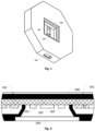
- Figure 1 shows a schematic representation of an embodiment of enclosure, bottom view, where rip 100 is used to allow light passing from emitters 101 to substrate where is reflected and back into photodiode sensor 102. Lateral opening is used by a USB 103 cable connection to power supply apparatus and for communication purposes.
- Figure 2 shows a detailed transversal representation of a cut of enclosure where it can be seen PCB 200 with upside down SMT components 201, in center photodiode sensor 202 and side by side the two light emitters 203.
- PCB 200 with upside down SMT components 201, in center photodiode sensor 202 and side by side the two light emitters 203.
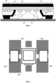
- Figure 3 shows a detailed transversal cut of enclosure 300 where it can be seen upside down SMT emitters 301 and photodiode sensor 302 with respective light angles scheme, incidence 303 and return 304 over and from the substrate 305.
- Figure 4 shows a schematic representation of an embodiment PCB layout for two LED 400 placed side by side of photodiode sensor 401; the gray squares are SMT solder pads 402.
- Figure 5 shows a schematic representation of an embodiment preferable for a PCB layout for two SMT LED 500 and two SMT photodiodes sensors 501; the gray forms are SMT solder pads 502.
- FIG. 6 shows a block diagram of modules microcontroller divided by main functionalities (processor with DSP instructions 600, ADC 601 with different input channels, DAC 602, RAM and flash memory 603, power supply with battery and battery charger circuit 604, several external communication possibilities 605 such as USB, Bluetooth, WiFi among other possibilities).
- main functionalities processor with DSP instructions 600, ADC 601 with different input channels, DAC 602, RAM and flash memory 603, power supply with battery and battery charger circuit 604, several external communication possibilities 605 such as USB, Bluetooth, WiFi among other possibilities).
- Figure 7 shows a detailed circuit of photodiode 700 with logarithm OP-AMP 701 made by loop gain diodes 702 and resistor 703.
- Figure 8 shows a drive circuit for IR or UV LEDs 800, controlled by DAC signal with OP-AMP 801 and constant current power source 802.
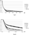
- Figure 9 shows the results got from embodiment with one photodiode sensor for a given substrate where LNPs are present with 400ppm, 100ppm, 10ppm, no LNPs and black body (only apparatus reflections).
- Figure 10 shows the results got from embodiment with one OP-AMP logarithm circuit and second stage OP-AMP circuit for a given LNP with 10ppm concentration.
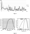
- Figure 11 shows the results got from embodiment with two different photodiodes sensors, for a set of substrates, where LNP07 and LNP08 are present in different sets of concentrations.
- Graphic is showing the Root Mean Square Deviation of difference between photodiodes signals, function in time.
- Figure 12 shows the Illustration of the wavelength spectral response of two different photodiodes of different suppliers.
- the enclosure rip and cavity will work as a dark chamber where an acrylic glass is placed on front.
- This acrylic glass has the function to protect emitters and sensors against dust and dirty, also is used for visible light cut filter. Dimensions are playing with direction and angle of incident light beam on substrate and respective reflective energy traveling back to the photodiode sensor.
- the sensor will have also an optimum angle and optimum direction where maximises the converted of received energy to electrical signal.
- the sensor electrical signal needs to be amplified and accommodate to ADC levels enabling to be analysed. It is disclosing the use of a logarithm OP-AMP based circuit giving a large amplification for small signals. Additionally, a second stage of a linear amplification, on output of logarithm OP-AMP based circuit, is used to increase more sensitivity.
- a true dark chamber is mandatory but not enough, light pass through the rip enclosure of the apparatus and only IR or UV light belonging to LEDs and LNPs emission. Enclosure has a flat surface where acrylic filter is completed align and without any gaps allowing a perfect contact with substrates. Apparatus is put down on a given substrate and before the illumination of substrate with IR or UV light, the dark level is measured. Under such conditions, if the photodiodes receive a level of signal over what was defined for the limit, the user is informed for the fact giving the chance to move apparatus for a better position.
- the process of a data acquisition is going to start by ADC where DAC level goes to maximum level of IR or UV light and loops decreasing intensity step by step.
- the signal obtained need to have a form as figure 9 allowing apparatus to be used for identification and quantification. Understanding the term identification as recognition of a given LNP presented in substrate and the term quantification the concentration of LNPs in substrate.
- identification and quantification values are stored in a remote storage infrastructure: database or block-chain.
- apparatus is connected using a USB cable with an external device as smartphone, tablet or even a computer.
- This external unit by user request, starts an acquisition informing apparatus for location, date and time.
- the apparatus receiving such information from external device creates then a package information with identification and quantification parameters added by location, date and time. In the end, send package information to remote storage infrastructure.
- each photodiode is inversed polarised where signal is amplified by independent OP-AMP logarithm-based circuit connected to different ADC's channels.
- VBP104FAS from Vishay Semiconductors which has a good response to infra-red light. Similar devices with different spectral response are use from others manufactures such as OSRAM, ON SMICONDUCTOR among others.
- Infra-red or ultraviolet emitters are driven by an ON-OFF circuit together with OP-AMP connected to DAC enabling to control current circuit varying light intensity.
- the IR LED's drive is power supply by a constant current circuit.
- the infra-red emitters are LED base component with high power and narrow beam from OSRAM Opto Semiconductors, reference SFH4640 where, according with manufacture, radiant intensity can reach 1050 mW/sr.
- a micro-controller is used to adequate infra-red or ultraviolet light to medium and acquiring data for post processing.
- the preferable embodiment by using a DAC output from a microcontroller, can adjust the intensity of infra-red light and also controlling signal format. With these intensity and time control the apparatus can adequate or tune IR or UV LEDs to the observed substrate taking the maximum level of reflect energy from LNPs and avoids photodiodes sensors saturation. Doing this light control, a tune process, apparatus increases the range of detection special for high concentration of LNPs.
- light control is in regard to control circuitry that is configured, such as a processor executing code that has start and end parameters the define a window of time in which LNP detection is performed, for instance, to ensure that detection of LNPs is performed after receiver obfuscation has subsided/concluded and such performance is before the signal is quenched by the material under observation.
- the photodiode sensor is amplified by a logarithm OP-AMP circuit where the result, input signal in ADC, is a line, function of time where the slope is directly proportional to the decay time of LN P.
- Quantification of a given substrate with LNPs is related to the time when light energy reaches the dark level.
- an apparatus comprising a dark chamber enclosure for recognising infrared, IR, and ultraviolet, UV, reactive luminescent nano-particles in a substrate using a set of sensors, said device comprising: one or more IR or UV illuminators for illuminating the luminescent nano-particles; a rip to allow light pass through; a drive based on constant current source; set of sensors based on photodiodes; a set of logarithm amplifiers OP-AMP based; a microcontroller with several ADC input channels and DAC output; wherein all photodiodes are different in terms of spectral sensitivity response; wherein all photodiodes has independent logarithm amplifiers circuits; wherein all independent photodiodes logarithm amplifiers signal are connected to different microcontroller ADC input channels; wherein IR or UV illuminators drive is controlled by a DAC microcontroller signal.
Landscapes
- Health & Medical Sciences (AREA)
- Chemical & Material Sciences (AREA)
- Immunology (AREA)
- Life Sciences & Earth Sciences (AREA)
- Physics & Mathematics (AREA)
- General Physics & Mathematics (AREA)
- Pathology (AREA)
- Analytical Chemistry (AREA)
- Biochemistry (AREA)
- General Health & Medical Sciences (AREA)
- Engineering & Computer Science (AREA)
- Nuclear Medicine, Radiotherapy & Molecular Imaging (AREA)
- Signal Processing (AREA)
- Dispersion Chemistry (AREA)
- Materials Engineering (AREA)
- Textile Engineering (AREA)
- Molecular Biology (AREA)
- Chemical Kinetics & Catalysis (AREA)
- Optics & Photonics (AREA)
- Investigating, Analyzing Materials By Fluorescence Or Luminescence (AREA)
Applications Claiming Priority (1)
| Application Number | Priority Date | Filing Date | Title |
|---|---|---|---|
| PT11854423 | 2023-03-07 |
Publications (2)
| Publication Number | Publication Date |
|---|---|
| EP4428527A2 true EP4428527A2 (de) | 2024-09-11 |
| EP4428527A3 EP4428527A3 (de) | 2024-09-18 |
Family
ID=92300478
Family Applications (1)
| Application Number | Title | Priority Date | Filing Date |
|---|---|---|---|
| EP24162210.9A Pending EP4428527A3 (de) | 2023-03-07 | 2024-03-07 | Vorrichtung und verfahren zur detektion reaktiver leuchtstoffpartikel in kohlenstoffbasierten nanomaterialien |
Country Status (2)
| Country | Link |
|---|---|
| US (1) | US12578257B2 (de) |
| EP (1) | EP4428527A3 (de) |
Citations (1)
| Publication number | Priority date | Publication date | Assignee | Title |
|---|---|---|---|---|
| WO1989008224A1 (en) | 1988-03-02 | 1989-09-08 | Brown David C | Luminescent fiber marker-detector |
Family Cites Families (11)
| Publication number | Priority date | Publication date | Assignee | Title |
|---|---|---|---|---|
| US4259574A (en) | 1979-11-06 | 1981-03-31 | International Business Machines Corporation | Microanalysis by pulse laser emission spectroscopy |
| GB2095822B (en) | 1981-03-30 | 1984-10-10 | Ramley Engineering Co Ltd | Identifying objects by detecting decaying phosphorescence from phosphor coating thereon |
| US4618257A (en) | 1984-01-06 | 1986-10-21 | Standard Change-Makers, Inc. | Color-sensitive currency verifier |
| US5757001A (en) | 1996-05-01 | 1998-05-26 | The Regents Of The University Of Calif. | Detection of counterfeit currency |
| AU4009901A (en) | 2000-03-07 | 2001-09-17 | Spectra Science Corporation | Quantum dots, semiconductor nanocrystals and semiconductor particles used as fluorescent coding elements |
| CN1950856B (zh) | 2004-03-08 | 2012-02-15 | 科学和工业研究理事会 | 使用积分透射和反射光谱响应的改进的验钞机 |
| US20130048874A1 (en) | 2011-08-31 | 2013-02-28 | Honeywell International Inc. | Articles with confounded emission characteristics and methods and apparatus for their authentication |
| US8947744B2 (en) * | 2012-06-19 | 2015-02-03 | Eastman Kodak Company | Spectral visible edge marking for steganography or watermarking |
| AU2018242894B2 (en) * | 2017-03-27 | 2020-11-05 | Glory Ltd. | Optical sensor, light detection apparatus, sheet processing apparatus, light detection method, and phosphorescence detection apparatus |
| DE102017129986A1 (de) | 2017-12-14 | 2019-06-19 | Sensor Instruments Entwicklungs- Und Vertriebs Gmbh | Vorrichtung für ein portables Smart-Gerät und Verfahren zur Produktprüfung |
| KR20220100889A (ko) | 2019-11-25 | 2022-07-18 | 스핀 앤 턴 - 컨설타도리아 데 소프트웨어, 엘디에이 | 반응성 발광 나노입자 또는 마이크로입자를 검출하기 위한 장치 및 방법 |
-
2024
- 2024-03-07 EP EP24162210.9A patent/EP4428527A3/de active Pending
- 2024-03-07 US US18/598,555 patent/US12578257B2/en active Active
Patent Citations (1)
| Publication number | Priority date | Publication date | Assignee | Title |
|---|---|---|---|---|
| WO1989008224A1 (en) | 1988-03-02 | 1989-09-08 | Brown David C | Luminescent fiber marker-detector |
Also Published As
| Publication number | Publication date |
|---|---|
| EP4428527A3 (de) | 2024-09-18 |
| US20250035533A1 (en) | 2025-01-30 |
| US12578257B2 (en) | 2026-03-17 |
Similar Documents
| Publication | Publication Date | Title |
|---|---|---|
| JPH11508352A (ja) | ルミネッセンスを高速にディジタル信号処理するモジュール化された計測システム | |
| CN105928911A (zh) | 一种荧光检测仪器的校准方法 | |
| CN112345115B (zh) | 一种基于双发光中心纳米晶近红外荧光的高灵敏测温方法 | |
| Hauser et al. | All-solid-state instrument for fluorescence-based fibre-optic chemical sensors | |
| CN202614177U (zh) | 硅片全面检测装置 | |
| US12578257B2 (en) | Device and method for detecting reactive luminescent particles in carbon-based nanomaterials | |
| US12050167B2 (en) | Device and method for detecting reactive luminescent nano- or micro- particles | |
| EP2288902B1 (de) | Vorrichtung zur bestimmung der elementbelegung auf einer glasoberfläche mittels fluoreszenz | |
| JP2807777B2 (ja) | スラブ光導波路を利用した光吸収スペクトル測定装置 | |
| AU2020393167B2 (en) | Device and method for detecting reactive luminescent nano- or micro- particles | |
| CN106970058A (zh) | 一种双荧光发射面的微量物质检测仪及检测方法 | |
| CN110779900A (zh) | 一种基于光纤超透镜的稀土离子上转换光谱高效测量系统 | |
| CN212780522U (zh) | 一种便携式溶解性有机物与浊度水质分析仪 | |
| CN212904531U (zh) | 一种基于手机的荧光便携显微检测仪 | |
| CN115372328B (zh) | 一种锂离子测量方法和装置 | |
| CN217425211U (zh) | 一种基于量子点荧光技术的高通量毛发毒品快速检测仪器 | |
| Schartner et al. | Lanthanide upconversion within microstructured optical fibers: improved detection limits for sensing and the demonstration of a new tool for nanocrystal characterization | |
| CN205982089U (zh) | 荧光检测仪 | |
| Venkataraj et al. | Chemically tapered multimode optical fiber probe for fluoride detection based on fluorescence quenching of curcumin | |
| EP2131183A1 (de) | Vorrichtung zur Bestimmung der Elementbelegung auf einer Oberfläche mittels Fluoreszenz | |
| CN210109119U (zh) | 免疫荧光定量分析仪 | |
| EP2686669B1 (de) | Verfahren zur messung der sauerstoffkonzentration in gasen | |
| CN100511262C (zh) | 一种光学防伪无损检测装置 | |
| CN223515076U (zh) | 一种光学传感器及其光源的光强控制电路 | |
| KR20210065686A (ko) | 광학식 비율 척도 기반 수질측정장치 |
Legal Events
| Date | Code | Title | Description |
|---|---|---|---|
| PUAI | Public reference made under article 153(3) epc to a published international application that has entered the european phase |
Free format text: ORIGINAL CODE: 0009012 |
|
| STAA | Information on the status of an ep patent application or granted ep patent |
Free format text: STATUS: THE APPLICATION HAS BEEN PUBLISHED |
|
| PUAL | Search report despatched |
Free format text: ORIGINAL CODE: 0009013 |
|
| AK | Designated contracting states |
Kind code of ref document: A2 Designated state(s): AL AT BE BG CH CY CZ DE DK EE ES FI FR GB GR HR HU IE IS IT LI LT LU LV MC ME MK MT NL NO PL PT RO RS SE SI SK SM TR |
|
| AK | Designated contracting states |
Kind code of ref document: A3 Designated state(s): AL AT BE BG CH CY CZ DE DK EE ES FI FR GB GR HR HU IE IS IT LI LT LU LV MC ME MK MT NL NO PL PT RO RS SE SI SK SM TR |
|
| RIC1 | Information provided on ipc code assigned before grant |
Ipc: G01N 21/64 20060101AFI20240813BHEP |
|
| STAA | Information on the status of an ep patent application or granted ep patent |
Free format text: STATUS: REQUEST FOR EXAMINATION WAS MADE |
|
| 17P | Request for examination filed |
Effective date: 20250317 |