EP4428268A1 - Diamond laminate - Google Patents
Diamond laminate Download PDFInfo
- Publication number
- EP4428268A1 EP4428268A1 EP22889993.6A EP22889993A EP4428268A1 EP 4428268 A1 EP4428268 A1 EP 4428268A1 EP 22889993 A EP22889993 A EP 22889993A EP 4428268 A1 EP4428268 A1 EP 4428268A1
- Authority
- EP
- European Patent Office
- Prior art keywords
- atoms
- laminate
- layer
- substrate
- electrode
- Prior art date
- Legal status (The legal status is an assumption and is not a legal conclusion. Google has not performed a legal analysis and makes no representation as to the accuracy of the status listed.)
- Pending
Links
Images



Classifications
-
- C—CHEMISTRY; METALLURGY
- C01—INORGANIC CHEMISTRY
- C01B—NON-METALLIC ELEMENTS; COMPOUNDS THEREOF; METALLOIDS OR COMPOUNDS THEREOF NOT COVERED BY SUBCLASS C01C
- C01B32/00—Carbon; Compounds thereof
- C01B32/25—Diamond
-
- C—CHEMISTRY; METALLURGY
- C25—ELECTROLYTIC OR ELECTROPHORETIC PROCESSES; APPARATUS THEREFOR
- C25B—ELECTROLYTIC OR ELECTROPHORETIC PROCESSES FOR THE PRODUCTION OF COMPOUNDS OR NON-METALS; APPARATUS THEREFOR
- C25B11/00—Electrodes; Manufacture thereof not otherwise provided for
- C25B11/04—Electrodes; Manufacture thereof not otherwise provided for characterised by the material
- C25B11/042—Electrodes formed of a single material
- C25B11/043—Carbon, e.g. diamond or graphene
-
- B—PERFORMING OPERATIONS; TRANSPORTING
- B32—LAYERED PRODUCTS
- B32B—LAYERED PRODUCTS, i.e. PRODUCTS BUILT-UP OF STRATA OF FLAT OR NON-FLAT, e.g. CELLULAR OR HONEYCOMB, FORM
- B32B9/00—Layered products comprising a layer of a particular substance not covered by groups B32B11/00 - B32B29/00
-
- C—CHEMISTRY; METALLURGY
- C01—INORGANIC CHEMISTRY
- C01B—NON-METALLIC ELEMENTS; COMPOUNDS THEREOF; METALLOIDS OR COMPOUNDS THEREOF NOT COVERED BY SUBCLASS C01C
- C01B32/00—Carbon; Compounds thereof
- C01B32/40—Carbon monoxide
-
- C—CHEMISTRY; METALLURGY
- C25—ELECTROLYTIC OR ELECTROPHORETIC PROCESSES; APPARATUS THEREFOR
- C25B—ELECTROLYTIC OR ELECTROPHORETIC PROCESSES FOR THE PRODUCTION OF COMPOUNDS OR NON-METALS; APPARATUS THEREFOR
- C25B1/00—Electrolytic production of inorganic compounds or non-metals
- C25B1/50—Processes
- C25B1/55—Photoelectrolysis
-
- C—CHEMISTRY; METALLURGY
- C25—ELECTROLYTIC OR ELECTROPHORETIC PROCESSES; APPARATUS THEREFOR
- C25B—ELECTROLYTIC OR ELECTROPHORETIC PROCESSES FOR THE PRODUCTION OF COMPOUNDS OR NON-METALS; APPARATUS THEREFOR
- C25B11/00—Electrodes; Manufacture thereof not otherwise provided for
- C25B11/04—Electrodes; Manufacture thereof not otherwise provided for characterised by the material
- C25B11/051—Electrodes formed of electrocatalysts on a substrate or carrier
- C25B11/052—Electrodes comprising one or more electrocatalytic coatings on a substrate
-
- C—CHEMISTRY; METALLURGY
- C25—ELECTROLYTIC OR ELECTROPHORETIC PROCESSES; APPARATUS THEREFOR
- C25B—ELECTROLYTIC OR ELECTROPHORETIC PROCESSES FOR THE PRODUCTION OF COMPOUNDS OR NON-METALS; APPARATUS THEREFOR
- C25B11/00—Electrodes; Manufacture thereof not otherwise provided for
- C25B11/04—Electrodes; Manufacture thereof not otherwise provided for characterised by the material
- C25B11/051—Electrodes formed of electrocatalysts on a substrate or carrier
- C25B11/055—Electrodes formed of electrocatalysts on a substrate or carrier characterised by the substrate or carrier material
- C25B11/057—Electrodes formed of electrocatalysts on a substrate or carrier characterised by the substrate or carrier material consisting of a single element or compound
- C25B11/065—Carbon
-
- C—CHEMISTRY; METALLURGY
- C25—ELECTROLYTIC OR ELECTROPHORETIC PROCESSES; APPARATUS THEREFOR
- C25B—ELECTROLYTIC OR ELECTROPHORETIC PROCESSES FOR THE PRODUCTION OF COMPOUNDS OR NON-METALS; APPARATUS THEREFOR
- C25B11/00—Electrodes; Manufacture thereof not otherwise provided for
- C25B11/04—Electrodes; Manufacture thereof not otherwise provided for characterised by the material
- C25B11/051—Electrodes formed of electrocatalysts on a substrate or carrier
- C25B11/073—Electrodes formed of electrocatalysts on a substrate or carrier characterised by the electrocatalyst material
- C25B11/075—Electrodes formed of electrocatalysts on a substrate or carrier characterised by the electrocatalyst material consisting of a single catalytic element or catalytic compound
- C25B11/083—Diamond
-
- C—CHEMISTRY; METALLURGY
- C25—ELECTROLYTIC OR ELECTROPHORETIC PROCESSES; APPARATUS THEREFOR
- C25B—ELECTROLYTIC OR ELECTROPHORETIC PROCESSES FOR THE PRODUCTION OF COMPOUNDS OR NON-METALS; APPARATUS THEREFOR
- C25B11/00—Electrodes; Manufacture thereof not otherwise provided for
- C25B11/04—Electrodes; Manufacture thereof not otherwise provided for characterised by the material
- C25B11/051—Electrodes formed of electrocatalysts on a substrate or carrier
- C25B11/073—Electrodes formed of electrocatalysts on a substrate or carrier characterised by the electrocatalyst material
- C25B11/075—Electrodes formed of electrocatalysts on a substrate or carrier characterised by the electrocatalyst material consisting of a single catalytic element or catalytic compound
- C25B11/087—Photocatalytic compound
-
- C—CHEMISTRY; METALLURGY
- C25—ELECTROLYTIC OR ELECTROPHORETIC PROCESSES; APPARATUS THEREFOR
- C25B—ELECTROLYTIC OR ELECTROPHORETIC PROCESSES FOR THE PRODUCTION OF COMPOUNDS OR NON-METALS; APPARATUS THEREFOR
- C25B9/00—Cells or assemblies of cells; Constructional parts of cells; Assemblies of constructional parts, e.g. electrode-diaphragm assemblies; Process-related cell features
-
- C—CHEMISTRY; METALLURGY
- C25—ELECTROLYTIC OR ELECTROPHORETIC PROCESSES; APPARATUS THEREFOR
- C25B—ELECTROLYTIC OR ELECTROPHORETIC PROCESSES FOR THE PRODUCTION OF COMPOUNDS OR NON-METALS; APPARATUS THEREFOR
- C25B9/00—Cells or assemblies of cells; Constructional parts of cells; Assemblies of constructional parts, e.g. electrode-diaphragm assemblies; Process-related cell features
- C25B9/50—Cells or assemblies of cells comprising photoelectrodes; Assemblies of constructional parts thereof
-
- C—CHEMISTRY; METALLURGY
- C25—ELECTROLYTIC OR ELECTROPHORETIC PROCESSES; APPARATUS THEREFOR
- C25B—ELECTROLYTIC OR ELECTROPHORETIC PROCESSES FOR THE PRODUCTION OF COMPOUNDS OR NON-METALS; APPARATUS THEREFOR
- C25B1/00—Electrolytic production of inorganic compounds or non-metals
- C25B1/01—Products
- C25B1/23—Carbon monoxide or syngas
Definitions
- the present disclosure relates to a novel diamond laminate and a method for producing the diamond laminate, and also relates to an electrode and an electrolytic reaction apparatus in which the diamond laminate is used, and to a method for producing carbon monoxide from carbon dioxide using the diamond laminate.
- the present disclosure claims the priority to US 63/276,348 provisionally filed in the United States on November 5, 2021 and JP 2021-186365 filed in Japan on November 16, 2021 , the contents of which are incorporated herein by reference.
- CO which is one of the reduction products of CO 2 , is particularly useful in that it is easy to handle because it is a gas, and it can be used in various applications.
- Patent Document 1 describes an invention in which CO 2 is reduced to produce CO through an electrochemical reaction using a reduction electrode provided with a catalyst layer that carries a precious metal such as Au, Ag, or Pt.
- a precious metal such as Au, Ag, or Pt.
- this method is problematic in that precious metals are generally expensive, and the reaction (CO 2 reduction reaction) in which CO 2 is reduced to CO competes with a reaction (H 2 O reduction reaction) in which water is reduced to hydrogen, and therefore the production efficiency of CO is low.
- Patent Document 2 indicates that in an electrochemical reaction using a reduction electrode containing a boron-doped diamond, irradiation with deep ultraviolet light excites electrons in the boron-doped diamond, and further application of a voltage causes a CO 2 reduction reaction to efficiently proceed.
- the CO 2 reduction reaction can proceed while the hydrogen reduction reaction is suppressed.
- voltage application and irradiation with ultraviolet light are required to cause the CO 2 reduction reaction to proceed, and thus a demand has existed for a technique to efficiently reduce CO 2 and produce CO using less energy.
- an object of the present disclosure is to provide a diamond laminate that exhibits an excellent electron emission capability and can form an electrode reaction field with an excellent reducing property.
- Another object of the present disclosure is to provide a method for producing the diamond laminate.
- Another object of the present disclosure is to provide an electrode in which the diamond laminate is used.
- Another object of the present disclosure is to provide an electrolytic reaction apparatus in which the diamond laminate is used.
- Another object of the present disclosure is to provide a method for producing carbon monoxide from carbon dioxide through an electrolytic reduction reaction in which the diamond laminate is used.
- the present disclosure provides a laminate including:
- the present disclosure also provides the laminate, wherein the nitrogen atom concentration in the layer (1) is 5 ⁇ 10 18 atoms/cm 3 or greater, and the boron atom concentration in the layer (2) is 1 ⁇ 10 19 atoms/cm 3 or greater.
- the present disclosure also provides the laminate, wherein the thickness of the layer (1) is from 1 nm to 100 ⁇ m, and the thickness of the layer (2) is 1 ⁇ m or greater.
- the present disclosure also provides a method for producing a laminate, the method including laminating an electron excitation layer (1) having a diamond crystal structure in which some carbon atoms are substituted with nitrogen atoms, and a conductive layer (2) having a diamond crystal structure in which some carbon atoms are substituted with boron atoms, to obtain the laminate.
- the present disclosure also provides an electrode including the laminate.
- the present disclosure also provides a method for producing carbon monoxide, the method including reducing, under irradiation with visible light, carbon dioxide on the electrode to obtain carbon monoxide.
- the diamond laminate of the present invention has a high total reduction current density (or since the total reduction current density is high and the Faradaic efficiency for CO production is excellent), the diamond laminate, when irradiated with visible light, easily emits electrons and forms a reaction field that exhibits an excellent reducing property. Therefore, in the photo-electrochemical field, the diamond laminate is suitable as a material for a low environmental load-type reduction electrode that uses sunlight as the energy required for a reduction reaction, or as a material for a visible light-responsive reduction electrode.
- a laminate according to an embodiment of the present disclosure includes an electron excitation layer (1) (NDD) having a diamond crystal structure in which some carbon atoms are substituted with nitrogen atoms, and a conductive layer (2) (BDD) having a diamond crystal structure in which some carbon atoms are substituted with boron atoms.
- NDD electron excitation layer
- BDD conductive layer (2)
- the laminate has a thickness of, for example, 1001 nm or greater, preferably 1010 nm or greater, and particularly preferably 1050 nm or greater.
- the upper limit of the thickness is, for example, 1 mm and preferably 500 ⁇ m.
- the laminate can emit electrons when irradiated with visible light.
- This electron emission capability (a value of electron emission current emitted per unit area during operation (for example, at a collector voltage of 100 V)) of the laminate is measured by a method described in the examples and is, for example, 10 pA/cm 2 or greater, and preferably 100 pA/cm 2 or greater. Therefore, the laminate can be suitably used for a low environmental load-type electrode (preferably, a reduction electrode) that can use sunlight as the energy source necessary for a reduction reaction.
- a low environmental load-type electrode preferably, a reduction electrode
- the electron excitation layer (1) is a layer having a diamond crystal structure in which some of the carbon atoms are substituted with nitrogen atoms.
- the electron excitation layer (1) contains carbon atoms and also nitrogen atoms as atoms other than the carbon atoms (that is, as heteroatoms).
- the nitrogen atom concentration of the layer (1) is, for example, 5 ⁇ 10 18 atoms/cm 3 or greater, preferably 1 ⁇ 10 19 atoms/cm 3 or greater, particularly preferably 5 ⁇ 10 19 atoms/cm 3 or greater, and especially preferably 1 ⁇ 10 20 atoms/cm 3 or greater.
- the upper limit of the nitrogen atom concentration is, for example, 5 ⁇ 10 22 atoms/cm 3 , preferably 1 ⁇ 10 22 atoms/cm 3 or less, particularly preferably 5 ⁇ 10 21 atoms/cm 3 or less, and most preferably 4 ⁇ 10 21 atoms/cm 3 or less.
- the layer (1) contains nitrogen atoms in the above range, the layer (1) has visible light responsiveness, and when the layer (1) is irradiated with visible light, electrons are easily transitioned to an excited state and emitted.
- the nitrogen atom concentration is less than the above range, the electron emission capability tends to be insufficient.
- the nitrogen atom concentration exceeds the above range, the diamond crystal structure is likely to collapse, and the electron emission performance tends to decrease.
- the layer (1) has a thickness of, for example, from 1 nm to 100 ⁇ m.
- the lower limit of the thicknesses of the layer (1) is preferably 3 nm or greater, more preferably 5 nm or greater, even more preferably 10 nm or greater, yet even more preferably 15 nm or greater, still even more preferably 30 nm or greater, even further preferably 40 nm or greater, particularly preferably 45 nm or greater, most preferably 50 nm or greater, and especially preferably 60 nm or greater.
- the upper limit of the thickness is preferably 10 ⁇ m, particularly preferably 1 ⁇ m, and most preferably 100 nm.
- the thickness of the layer (1) When the thickness of the layer (1) is less than the above range, the usage efficiency of visible light for electron excitation decreases, and the electron emission capability tends to become insufficient. On the other hand, when the thickness of the layer (1) exceeds the above range, the amount of electron excitation through visible light irradiation becomes saturated, and the electrical resistance increases, and therefore the reducing property tends to decrease.
- the concentration of nitrogen atoms in the layer (1) may be uniform or may be inclined from the surface portion towards the bottom portion. In the layer (1), when the nitrogen atom concentration increases from the bottom portion towards the surface layer portion, the electron emission capability tends to be further improved.
- the surface portion of the layer (1) is a portion near the surface of the layer (1) on the side opposite the side bonded to the conductive layer (2), and is, for example, a portion from the surface (depth of 0) to a depth of 60 nm (preferably 40 nm, and particularly preferably 20 nm).
- the nitrogen atom concentration of the surface layer portion of the layer (1) is, for example, 1 ⁇ 10 19 atoms/cm 3 or greater, preferably 5 ⁇ 10 19 atoms/cm 3 or greater, more preferably 1 ⁇ 10 20 atoms/cm 3 or greater, even more preferably 2 ⁇ 10 20 atoms/cm 3 or greater, particularly preferably 3 ⁇ 10 20 atoms/cm 3 or greater, and most preferably 4 ⁇ 10 20 atoms/cm 3 or greater.
- the upper limit of the nitrogen atom concentration is, for example, 5 ⁇ 10 22 atoms/cm 3 , preferably 1 ⁇ 10 21 atoms/cm 3 , and more preferably 5 ⁇ 10 21 atoms/cm 3 .
- the layer (1) may contain heteroatoms other than the nitrogen atom, and for example, may contain boron atoms.
- the concentration of the boron atoms is, for example, 1 ⁇ 10 13 atoms/cm 3 or greater, preferably 1 ⁇ 10 14 atoms/cm 3 or greater, more preferably 1 ⁇ 10 15 atoms/cm 3 or greater, even more preferably 1 ⁇ 10 16 atoms/cm 3 or greater, yet even more preferably 1 ⁇ 10 17 atoms/cm 3 or greater, still even more preferably 1 ⁇ 10 18 atoms/cm 3 or greater, even further preferably 1 ⁇ 10 19 atoms/cm 3 or greater, yet even further preferably 5 ⁇ 10 19 atoms/cm 3 or greater, particularly preferably 3 ⁇ 10 20 atoms/cm 3 or greater, most preferably 5 ⁇ 10 20 atoms/cm 3 or greater, and especially preferably 1 ⁇ 10 21 atoms/cm 3 or greater.
- the upper limit of the boron atom concentration is, for example, 5 ⁇ 10 22 atoms/cm 3 , preferably 3 ⁇ 10 22 atoms/cm 3 , and particularly preferably 1 ⁇ 10 22 atoms/cm 3 .
- the layer (1) may further contain other heteroatoms in addition to boron atoms and nitrogen atoms, and the concentration of the other heteroatoms is, for example, preferably 5 ⁇ 10 21 atoms/cm 3 or less from the viewpoint of having a high electron emission capability, and is more preferably 5 ⁇ 10 20 atoms/cm 3 or less, even more preferably 5 ⁇ 10 19 atoms/cm 3 or less, yet even more preferably 5 ⁇ 10 18 atoms/cm 3 or less, particularly preferably 1 ⁇ 10 18 atoms/cm 3 or less, most preferably 1 ⁇ 10 17 atoms/cm 3 or less, and especially preferably 1 ⁇ 10 16 atoms/cm 3 or less.
- the concentration of the other heteroatoms is, for example, preferably 5 ⁇ 10 21 atoms/cm 3 or less from the viewpoint of having a high electron emission capability, and is more preferably 5 ⁇ 10 20 atoms/cm 3 or less, even more preferably 5 ⁇ 10 19
- the heteroatom content (nitrogen atom content and boron atom content) in the layer and the thickness of the layer are determined by secondary ion mass spectrometry (SIMS) or the like.
- the surface layer portion of the layer (1) is preferably hydrogen-terminated. By hydrogen-terminating the surface layer portion, negative electron affinity increases and electrons are easily released.
- the conductive layer (2) is a layer having a diamond crystal structure in which some of the carbon atoms are substituted with boron atoms.
- the conductive layer (2) contains carbon atoms and also boron atoms as heteroatoms.
- the boron atom concentration in the layer (2) is, for example, 1 ⁇ 10 19 atoms/cm 3 or greater, preferably 5 ⁇ 10 19 atoms/cm 3 or greater, particularly preferably 3 ⁇ 10 20 atoms/cm 3 or greater, and especially preferably 1 ⁇ 10 21 atoms/cm 3 or greater.
- the upper limit of the boron atom concentration is, for example, 5 ⁇ 10 22 atoms/cm 3 , preferably 3 ⁇ 10 22 atoms/cm 3 , particularly preferably 1 ⁇ 10 22 atoms/cm 3 , most preferably 5 ⁇ 10 21 atoms/cm 3 or less, and especially preferably 3 ⁇ 10 21 atoms/cm 3 or less.
- the layer (2) contains boron atoms in the above range, the layer (2) has excellent conductivity.
- the boron atom concentration is less than the above range, the conductivity tends to become insufficient.
- the boron atom concentration exceeds the above range, the diamond crystal structure tends to easily collapse.
- the layer (2) may contain heteroatoms other than boron atoms, but the concentration of the heteroatoms other than boron atoms is, for example, preferably 5 ⁇ 10 21 atoms/cm 3 or less from the viewpoint of providing high conductivity, and is more preferably 5 ⁇ 10 20 atoms/cm 3 or less, even more preferably 5 ⁇ 10 19 atoms/cm 3 or less, further preferably 1 ⁇ 10 19 atoms/cm 3 or less, particularly preferably 1 ⁇ 10 18 atoms/cm 3 or less, most preferably 1 ⁇ 10 17 atoms/cm 3 or less, and especially preferably 1 ⁇ 10 16 atoms/cm 3 or less.
- the layer (2) is not required to contain nitrogen atoms, and the nitrogen atom concentration may be, for example, 5 ⁇ 10 20 atoms/cm 3 or less, preferably 1 ⁇ 10 20 atoms/cm 3 or less, more preferably 1 ⁇ 10 19 atoms/cm 3 or less, even more preferably less than 5 ⁇ 10 18 atoms/cm 3 , preferably 1 ⁇ 10 18 atoms/cm 3 or less, and particularly preferably 1 ⁇ 10 17 atoms/cm 3 or less.
- the lower limit of the nitrogen atom concentration is, for example, 1 ⁇ 10 16 atoms/cm 3 .
- the thickness of the layer (2) (the total thickness when the layer (2) is formed from a plurality of layers) is not particularly limited, and is, for example, 1 ⁇ m or greater, preferably 50 ⁇ m or greater, and particularly preferably 100 ⁇ m or greater. When the thickness of the layer (2) is 100 ⁇ m or greater, the layer (2) has sufficient strength to be a self-supporting film and is easy to handle, and thus such a thickness is preferable.
- the upper limit of the thickness is, for example, 1 mm, and from the viewpoint of suppressing an increase in the electrical resistance value, the upper limit is preferably 500 ⁇ m, and particularly preferably 300 ⁇ m.
- the layer (1) and the layer (2) may be constituted by only the diamond crystal structure in which some of the carbon atoms are substituted with heteroatoms, or may contain another component in addition to the diamond crystal structure.
- the other component include a silicon compound (such as silicon carbide).
- the position at which the other component is contained is not particularly limited, and for example, the other component may be contained in, among the surface layer portion of the layer, a portion from the surface (depth of 0) to a depth of 1000 nm (preferably 150 nm, particularly preferably 20 nm).
- the content of the other component is, for example, 10 wt.% or less (for example, from 10 to 0.1 wt.%).
- the laminate according to an embodiment of the present disclosure may include another configuration in addition to the layers (1) and (2).
- the proportion of the total of the layers (1) and (2) in the total amount (100 wt.%) of the laminate according to an embodiment of the present disclosure is, for example, 60 wt.% or greater, preferably 70 wt.% or greater, more preferably 80 wt.% or greater, particularly preferably 90 wt.% or greater, and most preferably 95 wt.% or greater, in relation to the total amount of the laminate.
- the upper limit is 100 wt.%. That is, the laminate may be configured by only the layer (1) and the layer (2).
- the laminate described above can be produced by laminating an electron excitation layer (1) having a diamond crystal structure in which some carbon atoms are substituted with nitrogen atoms, and a conductive layer (2) having a diamond crystal structure in which some carbon atoms are substituted with boron atoms.
- the method for producing the laminate includes a production method through the following steps.
- Step 2 The following steps may also be provided after Step 2.
- Step 1 is a step of fixing nitrogen-containing diamond particles on a substrate.
- nitrogen-containing diamond particles are diamond particles containing nitrogen atoms, and the site at which a nitrogen atom is contained is not limited.
- the diamond particles are configured from a core part formed from sp3 carbons and a shell part formed from sp2 carbons, and the nitrogen atom may be contained in the core part or in the shell part. Further, the nitrogen atom may be contained in the boundary between the core part and the shell part.
- the method for fixing the nitrogen-containing diamond particles on the substrate is not particularly limited, and examples thereof include a method in which a paint containing nitrogen-containing diamond particles is applied onto the substrate and dried to fix the nitrogen-containing diamond particles on the substrate.
- the substrate is not particularly limited, and examples thereof include a silicon substrate, a quartz substrate, a ceramic substrate, a glass substrate, a metal substrate (e.g., an aluminum substrate, a copper substrate, an iron substrate, a stainless steel substrate, and a brass substrate), and a plastic substrate (e.g., a polyimide substrate and a polyamide substrate).
- a silicon substrate is preferable in that it excels in heat resistance, mass productivity, thermal shock resistance, and the like.
- the surface of the substrate may be subjected to ultrasonic cleaning with acetone, ethanol, pure water, or the like. Further, the surface of the substrate may also be subjected to an acid wash or the like with hydrochloric acid, hydrofluoric acid, or the like. In addition, fine unevenness may be formed on the surface of the substrate.
- the shape of the nitrogen-containing diamond particles is not particularly limited, and examples thereof include a spherical shape (e.g., a true spherical shape, a substantially true spherical shape, and an elliptically spherical shape), a polyhedral shape, a rod shape (e.g., a cylindrical shape, a prismatic shape), a flat plate shape, a flaky shape, and an irregular shape.
- a spherical shape e.g., a true spherical shape, a substantially true spherical shape, and an elliptically spherical shape
- a polyhedral shape e.g., a rod shape (e.g., a cylindrical shape, a prismatic shape)
- a flat plate shape e.g., a flat plate shape, a flaky shape, and an irregular shape.
- the nitrogen-containing diamond particles have an average particle size of, for example, from 1 nm to 100 ⁇ m. If the average particle size is less than the above range, the nitrogen-containing diamond particles are removed together with the substrate when the substrate is removed in Step 2, and this may make it difficult to form the electron excitation layer (1). On the other hand, when the average particle size exceeds the above range, the electron excitation layer (1) tends to become thick, the electrical resistance increases, and the reducing property tends to decrease. Note that the average particle size is the median diameter (d50) obtained by a laser diffraction/scattering method.
- the nitrogen-containing diamond particles are obtained, for example, by a method of adding a nitrogen source to a raw material when producing nanodiamond particles by a detonation method or the like, a method of obtaining a grown film containing nitrogen-doped diamonds obtained by a CVD method and pulverizing the obtained grown film, and a method of doping nitrogen atoms into undoped nanodiamond particles through an ion implantation method.
- the paint contains a solvent along with the nitrogen-containing diamond particles.
- the solvent include water; alcohols such as ethanol and propanol; hydrocarbons such as toluene; cyclic ethers such as tetrahydrofuran; and ketones such as methyl isobutyl ketone.
- one type of solvent may be used alone, or two or more types thereof may be used in combination.
- water and/or alcohols are preferable in terms of exhibiting excellent dispersibility of the nitrogen-containing nanodiamond particles.
- the paint may further contain a thickener, a dispersant, a buffering agent, and the like.
- the content of the nitrogen-containing diamond particles in the paint is, for example, from 0.001 to 5.0 wt.%, and preferably from 0.1 to 1.0 wt.%.
- the method for applying the paint is not particularly limited, and the paint can be applied through, for example, a printing method or a coating method.
- a printing method or a coating method include a screen printing method, a mask printing method, an offset printing method, an inkjet printing method, a flexographic printing method, a gravure printing method, stamping, dispensing, a squeegee printing method, a silk screen printing method, and brush coating.
- the paint may be applied only once or may be repeatedly applied a plurality of times, and from the viewpoint of producing an electron excitation layer (1) that can exhibit a sufficient electron emission capability, the paint is preferably repeatedly applied a plurality of times (for example, from 2 to 20 times, preferably from 5 to 15 times) to form a coating film having an appropriate thickness.
- the coating film has a thickness of, for example, from 1 nm to 100 ⁇ m, and can be appropriately selected according to the desired function.
- the lower limit of the coating film thickness is preferably 3 nm or greater, more preferably 10 nm or greater, particularly preferably 30 nm or greater, most preferably 50 nm or greater, and especially preferably 70 nm.
- the upper limit of the coating film thickness is preferably 10 ⁇ m, particularly preferably 1 ⁇ m, and most preferably 100 nm.
- the lower limit of the coating film thickness is preferably 3 nm or greater, and particularly preferably 5 nm or greater.
- the upper limit of the coating film thickness is preferably 10 ⁇ m, particularly preferably 1 ⁇ m, and most preferably 100 nm.
- a method is preferably adopted in which, for example, a below-described Step I is carried out once, after which a below-described Step II is carried out at least once.
- Step I applying, onto a substrate having a positive or negative charge, a paint containing diamond particles having a positive or negative charge, of which the charge is opposite the charge of the substrate, to fix the diamond particles on the substrate.
- Step II applying, onto the fixed diamond particles, a paint containing diamond particles having a positive or negative charge, of which the charge is opposite the charge of the fixed diamond particles, to laminate the diamond particles having the opposite charge onto the fixed diamond particles.
- Step I when the paint containing diamond particles having a charge opposite the charge of the substrate is applied onto the substrate, the diamond particles in the paint migrate towards the substrate due to Coulomb force. When the diamond particles approach the substrate, van der Waals force is added to the Coulomb force, and the diamond particles are adsorbed and fixed on the substrate.
- Step II the diamond particles in the aqueous dispersion migrate toward the fixed diamond particles due to the Coulomb force, and when the diamond particles approach each other, the diamond particles are adsorbed and fixed due to the addition of the van der Waals force to the Coulomb force.
- the amplitude is represented by the sum of the absolute value of the zeta potential of the fixed diamond particles and the absolute value of the zeta potential of the diamond particles having a charge opposite the charge of the fixed diamond particles, and is, for example, 40 mV or greater, preferably 50 mV or greater, more preferably 60 mV or greater, particularly preferably 65 mV or greater, most preferably 70 mV or greater, and especially preferably 80 mV or greater.
- the upper limit of the sum of the absolute values of the zeta potentials is, for example, 120 mV.
- Examples of the vapor phase growth method include a microwave plasma CVD method, a plasma CVD method, a hot-filament CVD method, and an optical CVD method.
- the microwave plasma CVD method is preferable in that a diamond crystal structure having excellent crystallinity can be rapidly formed.
- the microwave plasma CVD method is a method for growing a boron-doped diamond crystal structure by guiding microwaves into a plasma generation chamber to decompose a carbon source and a boron source and generate plasmas, and then guiding the plasma onto a substrate heated to a temperature from 300 to 900°C.
- the boron atom content in the resulting diamond crystal structure can be controlled by adjusting the blending amount of the boron source added to the carbon source.
- Examples of the carbon source include hydrocarbons such as methane, ethane, propane, ethylene, and acetylene; alcohols such as methanol and ethanol; and ketones such as acetone.
- hydrocarbons such as methane, ethane, propane, ethylene, and acetylene
- alcohols such as methanol and ethanol
- ketones such as acetone.
- One type of carbon source can be used alone, or two or more types thereof can be used in combination.
- Step 3 is a step of removing the substrate from the substrate/electron excitation layer (1)/conductive layer (2) laminate obtained through Step 2.
- the method for removing the substrate can be appropriately selected according to the type of substrate. For example, when a silicon substrate is used as the substrate, a method of dissolving and removing the substrate using a mixed solution of hydrofluoric acid and nitric acid can be selected.
- Step 4 is a step of hydrogenating the surface, exposed by removing the substrate, of the electron excitation layer (1)/conductive layer (2) laminate obtained through step 3, that is, the surface on the electron excitation layer (1) side.
- the surface of the electron excitation layer (1) can be hydrogenated by, for example, a hydrogen-plasma treatment.
- the method for producing the laminate may also include a production method through the following steps.
- Step 2' The following steps may also be provided after Step 2'.
- Step 1' can be carried out in the same manner as Step 2 described above with the exception that instead of forming the boron-doped diamond crystal structure on the substrate having nitrogen-containing diamond particles fixed to the surface, the boron-doped diamond crystal structure is formed on a substrate having seed crystals (e.g., diamond particles not containing nitrogen) fixed to the surface thereof.
- seed crystals e.g., diamond particles not containing nitrogen
- Step 2' can be carried out in the same manner as Step 1 described above with the exception that instead of applying the paint containing nitrogen-containing diamond particles onto the substrate, the paint containing nitrogen-containing diamond particles is applied onto the boron-doped diamond crystal structure obtained in step 1'.
- the laminate produced by the above method uses the nitrogen-containing diamond particles, the nitrogen atom concentration can be increased without damaging the diamond crystal structure of the electron excitation layer (1), and the laminate has both an electron emission capability stemming from the diamond crystal structure and good visible light responsiveness.
- the laminate is irradiated with visible light, electrons are emitted, and an electrode reaction field having an excellent reducing property is formed.
- the laminate has the above-described characteristics, it can be suitably used as a low environmental load-type electrode (preferably, a reduction electrode) that uses sunlight.
- An electrode according to an embodiment of the present disclosure includes the laminate.
- the electrode may be configured from only the laminate, or may be provided with another configuration.
- the laminate may be laminated on a known substrate.
- the electrode emits electrons by irradiation with visible light, and thereby forms a reaction field with an excellent reducing property. Therefore, the electrode is preferably a reduction electrode, particularly preferably a visible light-responsive reduction electrode, and most preferably a reduction electrode for photovoltaic power generation.
- An electrolytic reaction apparatus is provided with the above-described electrode (for example, a reduction electrode) or the above-described laminate.
- the electrolytic reaction apparatus may further include an oxidation electrode, a separator, an electrolytic cell, a power supply, and the like.
- the electrolytic reaction apparatus is preferably a reduction reaction apparatus.
- the electrode included in the electrolytic reaction apparatus has a function of emitting electrons (more specifically, solvated electrons) when irradiated with sunlight. Therefore, when the electrolytic reaction apparatus is used, an electrolytic reaction can be carried out using sunlight, and energy saving is achieved. When CO 2 is reduced using the electrolytic reaction apparatus, CO can be selectively and efficiently produced. The carbon monoxide thus produced can be used as a raw material for various chemical products.
- the amount of CO produced is, for example, 0.01 mol/m 2 ⁇ hr or greater, preferably 0.05 mol/m 2 ⁇ hr or greater, more preferably 0.1 mol/m 2 ⁇ hr or greater, and particularly preferably 0.15 mol/m 2 ⁇ hr or greater.
- a SiO 2 /Si substrate was used as a substrate.
- the SiO 2 /Si substrate was a laminate of SiO 2 (100 nm thick) and n-type Si (0.45 mm thick), and the diameter was 8 mm.
- the SiO 2 /Si substrate was subjected to an ultrasonic cleaning treatment with acetone, ethanol, and pure water and to an acid wash treatment.
- N-nD nitrogen-containing nanodiamond particles
- concentration of N-nD particles 1.0%, solvent: water
- the N-nD particle film surface of the obtained N-nD particle film/SiO 2 /Si substrate laminate was subjected to a hydrogen-plasma treatment (1) (900 W, 50 kPa, substrate temperature: 890°C, hydrogen flow rate: 100 sccm) for an arbitrary period of time within 1 hour to remove sp2 carbons of the N-nD particle film.
- a hydrogen-plasma treatment (1) 900 W, 50 kPa, substrate temperature: 890°C, hydrogen flow rate: 100 sccm
- BDD boron-doped nanodiamonds
- the obtained NDD/BDD laminate had a film thickness of 0.15 mm and was self-supporting.
- the NDD-side surface of the NDD/BDD laminate was subjected to a hydrogen-plasma treatment (2) (650 W, 40 kPa, 5 minutes, substrate temperature 850°C, hydrogen flow rate 100 sccm) to carry out hydrogen termination and remove sp2 carbons.
- a hydrogen-plasma treatment (2) 650 W, 40 kPa, 5 minutes, substrate temperature 850°C, hydrogen flow rate 100 sccm
- the CO 2 reduction capability was measured by the following method using the laminate (1) as a diamond electrode.
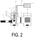
- the laminate (1) (the surface area in contact with the electrolytic solution was 0.2 cm 2 ) was used as a working electrode 1, and a platinum mesh electrode was used as a counter electrode 2.
- H-type cell available from EC Frontier Co., Ltd.
- the working electrode 1 and the reference electrode 3 were installed in the cathode chamber 9, and the counter electrode 2 was installed in the anode chamber 10.
- the two chambers were separated by a diaphragm 5 (Nafion 117), and then 30 mL of a 0.1 M potassium chloride aqueous solution were added as an electrolytic solution to each chamber.
- the H-type cell was then sealed, after which CO 2 gas was bubbled through an introduction port 6 at a flow rate of 80 mL/min for 30 minutes and released from a gas discharge port 8 to deaerate the electrolytic solution, and CO 2 was dissolved to a saturated concentration. While the CO 2 gas flow rate was maintained at 80 mL/min, a sample bag 7 (Smart Bag PA, CEK-1, available from GL Sciences Inc.) was attached, and application of a constant potential of -2.0 V (vs. Ag/AgCl) to the working electrode 1 was immediately started using an electrochemical measurement system (HSV-110, available from Hokuto Denko Corporation).
- HSV-110 electrochemical measurement system
- a gold foil was disposed on an insulating base in a measurement chamber (available from Riko International Ltd., i-Series ultra-high vacuum microprobe and chamber, vacuum degree of 10 -4 Pa or less, measurement temperature of 23 to 40°C), and the laminate (1) was disposed thereon and oriented such that the BDD side was in contact with the gold foil.
- a measurement chamber available from Riko International Ltd., i-Series ultra-high vacuum microprobe and chamber, vacuum degree of 10 -4 Pa or less, measurement temperature of 23 to 40°C
- a voltage of -20 V was then applied to the back surface of the laminate (1) using a semiconductor parameter analyzer (Keithley Semiconductor Characterization System 4200-SCS), a collector voltage (0 to 100 V) was applied at a position of 100 ⁇ m above the front surface of the laminate (1), and the laminate (1) was then irradiated with visible light from a position 35 mm away from the laminate (1) in the same manner as in the evaluation of the CO 2 reduction capability, and the amount of generated current was measured. The results are shown in FIG. 3 .
- Example 2 The CO 2 reduction capability and the electron emission efficiency were evaluated in the same manner as in Example 1 with the exception that a boron-doped diamond film (BDD) was used as the diamond electrode instead of the BDD/NDD laminate.
- BDD boron-doped diamond film
- a hydrogen-terminated NDD/BDD laminate was obtained in the same manner as in Example 1 with the exception that the thickness of the conductive layer (2) was changed.
- a hydrogen-terminated NDD/BDD laminate was obtained in the same manner as in Example 1 with the exception that the nitrogen atom concentration and the boron atom concentration were changed as described in the following table, and the hydrogen-plasma treatment (1) was not implemented.
- a SiO 2 /Si substrate was used as a substrate.
- the SiO 2 /Si substrate was a laminate of SiO 2 (100 nm thick) and n-type Si (0.45 mm thick), and the diameter was 8 mm.
- the SiO 2 /Si substrate was subjected to an ultrasonic cleaning treatment with acetone, ethanol, and pure water and to an acid wash treatment.
- a suspension of nitrogen-containing ⁇ + nanodiamond particles (particle size D50: 5 nm) (concentration of N- ⁇ +nD particles: 1.0%, solvent: water, zeta potential: +50 mV) was applied to the SiO 2 /Si substrate treated in the same manner as in Example 1, after which the substrate surface was thoroughly washed with pure water, and water remaining on the surface was removed by air blowing.
- a suspension of nitrogen-containing ⁇ - nanodiamond particles (particle size D50: 5 nm) (concentration of N- ⁇ -nD particles: 1.0%, solvent: water, zeta potential: -40 mV) was applied at room temperature onto the treated SiO 2 /Si substrate, after which the substrate surface was thoroughly washed with pure water, and water remaining on the surface was removed by air blowing.
- a BDD/NDD/SiO 2 /Si substrate laminate was obtained in the same manner as in Example 1 with the exception that the boron and nitrogen atom concentrations were changed as described in the following table, and the hydrogen-plasma treatment (1) was not carried out.
- N-nD particle film/SiO 2 /Si substrate laminate was obtained in the same manner as in Example 4 with the exception that the number of repetitions of the process of immersing in the suspension of nitrogen-containing ⁇ + nanodiamond particles, drying, immersing in the suspension of nitrogen-containing ⁇ - nanodiamond particles, and drying was changed.
- a BDD/NDD/SiO 2 /Si substrate laminate was obtained in the same manner as in Example 1 with the exception that the boron atom concentration and the thickness of the layer (2) were changed as described in the following table, and the hydrogen-plasma treatment (1) was not carried out.
- the laminates obtained in the Examples and the Comparative Example were used as electrodes, and the electron emission amount, the total reduction current density, and the Faradaic efficiency for CO production (CO-F efficiency) were measured by the following methods.
- the amount of current generated was measured by the same apparatus and method as in the evaluation of electron emission efficiency with the exception that the collector voltage was fixed to 0 V
- the total reduction current density was calculated by recording changes in the reduction current when a constant potential was applied for 15 minutes with the same apparatus and under the same conditions as in the evaluation of the CO 2 reduction capability, and then dividing an average value thereof by the electrode surface area.
- the diamond laminate of the present invention is suitable as a material of a low environmental load-type reduction electrode that uses sunlight as the energy required for a reduction reaction, or as a material of a visible light-responsive reduction electrode.
Landscapes
- Chemical & Material Sciences (AREA)
- Organic Chemistry (AREA)
- Engineering & Computer Science (AREA)
- Chemical Kinetics & Catalysis (AREA)
- Electrochemistry (AREA)
- Materials Engineering (AREA)
- Metallurgy (AREA)
- Inorganic Chemistry (AREA)
- Geology (AREA)
- General Life Sciences & Earth Sciences (AREA)
- Life Sciences & Earth Sciences (AREA)
- Crystals, And After-Treatments Of Crystals (AREA)
- Carbon And Carbon Compounds (AREA)
- Chemical Vapour Deposition (AREA)
Abstract
Description
- The present disclosure relates to a novel diamond laminate and a method for producing the diamond laminate, and also relates to an electrode and an electrolytic reaction apparatus in which the diamond laminate is used, and to a method for producing carbon monoxide from carbon dioxide using the diamond laminate. The present disclosure claims the priority to
US 63/276,348 provisionally filed in the United States on November 5, 2021 JP 2021-186365 filed in Japan on November 16, 2021 - Among carbon recycling techniques for converting CO2 contained in exhaust gas or the like into a useful chemical product, a technique for electrolytic reduction of CO2 is expected to have suppressed hydrogen generation, increased conversion efficiency of CO2, and increased product selectivity. CO, which is one of the reduction products of CO2, is particularly useful in that it is easy to handle because it is a gas, and it can be used in various applications.
-
Patent Document 1 describes an invention in which CO2 is reduced to produce CO through an electrochemical reaction using a reduction electrode provided with a catalyst layer that carries a precious metal such as Au, Ag, or Pt. However, this method is problematic in that precious metals are generally expensive, and the reaction (CO2 reduction reaction) in which CO2 is reduced to CO competes with a reaction (H2O reduction reaction) in which water is reduced to hydrogen, and therefore the production efficiency of CO is low. -
Patent Document 2 indicates that in an electrochemical reaction using a reduction electrode containing a boron-doped diamond, irradiation with deep ultraviolet light excites electrons in the boron-doped diamond, and further application of a voltage causes a CO2 reduction reaction to efficiently proceed. - Since the abovementioned boron-doped diamond has a wide potential window, the CO2 reduction reaction can proceed while the hydrogen reduction reaction is suppressed. However, as described above, voltage application and irradiation with ultraviolet light are required to cause the CO2 reduction reaction to proceed, and thus a demand has existed for a technique to efficiently reduce CO2 and produce CO using less energy.
-
- Patent Document 1:
JP 2020-132965 A - Patent Document 2:
JP 2017-100901 A - Therefore, an object of the present disclosure is to provide a diamond laminate that exhibits an excellent electron emission capability and can form an electrode reaction field with an excellent reducing property.
- Another object of the present disclosure is to provide a method for producing the diamond laminate.
- Another object of the present disclosure is to provide an electrode in which the diamond laminate is used.
- Another object of the present disclosure is to provide an electrolytic reaction apparatus in which the diamond laminate is used.
- Another object of the present disclosure is to provide a method for producing carbon monoxide from carbon dioxide through an electrolytic reduction reaction in which the diamond laminate is used.
- As a result of diligent research to solve the problems described above, the present inventors discovered the following. Namely,
- 1. In a nitrogen-containing diamond crystal structure, a donor level is formed at a position near the conduction band in a bandgap of the diamond by nitrogen atoms contained therein, and therefore the nitrogen-containing diamond crystal structure, when irradiated with visible light, easily transitions to an excited state and emits electrons.
- 2. A boron-doped diamond crystal structure exhibits excellent conductivity.
- 3. A laminate of the nitrogen-containing diamond crystal structure and the boron-doped diamond crystal structure forms a reaction field that is rich in a reducing property, and therefore such a laminate is useful as an electrode material.
- 4. When an electrochemical reaction is carried out using this laminate as a reduction electrode, a reduction reaction for producing CO from CO2 is selectively promoted, and CO can be efficiently produced.
- The present disclosure was completed on the basis of these findings.
- That is, the present disclosure provides a laminate including:
- an electron excitation layer (1) having a diamond crystal structure in which some carbon atoms are substituted with nitrogen atoms; and
- a conductive layer (2) having a diamond crystal structure in which some carbon atoms are substituted with boron atoms.
- The present disclosure also provides the laminate, wherein the nitrogen atom concentration in the layer (1) is 5 × 10¹⁸ atoms/cm3 or greater, and the boron atom concentration in the layer (2) is 1 × 10¹⁹ atoms/cm3 or greater.
- The present disclosure also provides the laminate, wherein the thickness of the layer (1) is from 1 nm to 100 µm, and the thickness of the layer (2) is 1 µm or greater.
- The present disclosure also provides a method for producing a laminate, the method including laminating an electron excitation layer (1) having a diamond crystal structure in which some carbon atoms are substituted with nitrogen atoms, and a conductive layer (2) having a diamond crystal structure in which some carbon atoms are substituted with boron atoms, to obtain the laminate.
- The present disclosure also provides an electrode including the laminate.
- The present disclosure also provides the electrode, wherein the electrode is a visible light-responsive reduction electrode.
- The present disclosure also provides an electrolytic reaction apparatus provided with the electrode.
- The present disclosure also provides a method for producing carbon monoxide, the method including reducing, under irradiation with visible light, carbon dioxide on the electrode to obtain carbon monoxide.
- Since the diamond laminate of the present invention has a high total reduction current density (or since the total reduction current density is high and the Faradaic efficiency for CO production is excellent), the diamond laminate, when irradiated with visible light, easily emits electrons and forms a reaction field that exhibits an excellent reducing property. Therefore, in the photo-electrochemical field, the diamond laminate is suitable as a material for a low environmental load-type reduction electrode that uses sunlight as the energy required for a reduction reaction, or as a material for a visible light-responsive reduction electrode.
-
-
FIG. 1 is a graph showing the results of an analysis of the concentrations of boron atoms and nitrogen atoms in a laminate obtained in Example 1. -
FIG. 2 is a schematic view of an H-type cell used for evaluating the CO production efficiency of a diamond electrode through CO2 reduction. -
FIG. 3 is a graph showing measurement results of electron emission currents of diamond electrodes obtained in Example 1 and Comparative Example 1. -
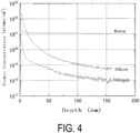
FIG. 4 is a graph showing the results of an analysis of the concentrations of boron atoms, nitrogen atoms, and silicon atoms in the laminate obtained in Example 1. -
FIG. 5 is a graph showing the results of an analysis of the concentrations of boron atoms, nitrogen atoms, and silicon atoms in a laminate obtained in Example 3. - A laminate according to an embodiment of the present disclosure includes an electron excitation layer (1) (NDD) having a diamond crystal structure in which some carbon atoms are substituted with nitrogen atoms, and a conductive layer (2) (BDD) having a diamond crystal structure in which some carbon atoms are substituted with boron atoms.
- The laminate has a thickness of, for example, 1001 nm or greater, preferably 1010 nm or greater, and particularly preferably 1050 nm or greater. The upper limit of the thickness is, for example, 1 mm and preferably 500 µm.
- The laminate can emit electrons when irradiated with visible light. This electron emission capability (a value of electron emission current emitted per unit area during operation (for example, at a collector voltage of 100 V)) of the laminate is measured by a method described in the examples and is, for example, 10 pA/cm2 or greater, and preferably 100 pA/cm2 or greater. Therefore, the laminate can be suitably used for a low environmental load-type electrode (preferably, a reduction electrode) that can use sunlight as the energy source necessary for a reduction reaction.
- The electron excitation layer (1) is a layer having a diamond crystal structure in which some of the carbon atoms are substituted with nitrogen atoms.
- The electron excitation layer (1) contains carbon atoms and also nitrogen atoms as atoms other than the carbon atoms (that is, as heteroatoms).
- The nitrogen atom concentration of the layer (1) is, for example, 5 × 10¹⁸ atoms/cm3 or greater, preferably 1 × 10¹⁹ atoms/cm3 or greater, particularly preferably 5 × 10¹⁹ atoms/cm3 or greater, and especially preferably 1 × 10²⁰ atoms/cm3 or greater. The upper limit of the nitrogen atom concentration is, for example, 5 × 10²² atoms/cm3, preferably 1 × 10²² atoms/cm3 or less, particularly preferably 5 × 10²¹ atoms/cm3 or less, and most preferably 4 × 10²¹ atoms/cm3 or less. Since the layer (1) contains nitrogen atoms in the above range, the layer (1) has visible light responsiveness, and when the layer (1) is irradiated with visible light, electrons are easily transitioned to an excited state and emitted. When the nitrogen atom concentration is less than the above range, the electron emission capability tends to be insufficient. On the other hand, when the nitrogen atom concentration exceeds the above range, the diamond crystal structure is likely to collapse, and the electron emission performance tends to decrease.
- The layer (1) has a thickness of, for example, from 1 nm to 100 µm. From the viewpoint of exhibiting sufficient electron emission capability, the lower limit of the thicknesses of the layer (1) is preferably 3 nm or greater, more preferably 5 nm or greater, even more preferably 10 nm or greater, yet even more preferably 15 nm or greater, still even more preferably 30 nm or greater, even further preferably 40 nm or greater, particularly preferably 45 nm or greater, most preferably 50 nm or greater, and especially preferably 60 nm or greater. From the viewpoint of suppressing electrical resistance, the upper limit of the thickness is preferably 10 µm, particularly preferably 1 µm, and most preferably 100 nm. When the thickness of the layer (1) is less than the above range, the usage efficiency of visible light for electron excitation decreases, and the electron emission capability tends to become insufficient. On the other hand, when the thickness of the layer (1) exceeds the above range, the amount of electron excitation through visible light irradiation becomes saturated, and the electrical resistance increases, and therefore the reducing property tends to decrease.
- The concentration of nitrogen atoms in the layer (1) may be uniform or may be inclined from the surface portion towards the bottom portion. In the layer (1), when the nitrogen atom concentration increases from the bottom portion towards the surface layer portion, the electron emission capability tends to be further improved. The surface portion of the layer (1) is a portion near the surface of the layer (1) on the side opposite the side bonded to the conductive layer (2), and is, for example, a portion from the surface (depth of 0) to a depth of 60 nm (preferably 40 nm, and particularly preferably 20 nm).
- The nitrogen atom concentration of the surface layer portion of the layer (1) is, for example, 1 × 10¹⁹ atoms/cm3 or greater, preferably 5 × 10¹⁹ atoms/cm3 or greater, more preferably 1 × 10²⁰ atoms/cm3 or greater, even more preferably 2 × 10²⁰ atoms/cm3 or greater, particularly preferably 3 × 10²⁰ atoms/cm3 or greater, and most preferably 4 × 10²⁰ atoms/cm3 or greater. The upper limit of the nitrogen atom concentration is, for example, 5 × 10²² atoms/cm3, preferably 1 × 10²¹ atoms/cm3, and more preferably 5 × 10²¹ atoms/cm3.
- The layer (1) may contain heteroatoms other than the nitrogen atom, and for example, may contain boron atoms.
- When the layer (1) contains boron atoms, the concentration of the boron atoms is, for example, 1 × 10¹³ atoms/cm3 or greater, preferably 1 × 10¹⁴ atoms/cm3 or greater, more preferably 1 × 10¹⁵ atoms/cm3 or greater, even more preferably 1 × 10¹⁶ atoms/cm3 or greater, yet even more preferably 1 × 10¹⁷ atoms/cm3 or greater, still even more preferably 1 × 10¹⁸ atoms/cm3 or greater, even further preferably 1 × 10¹⁹ atoms/cm3 or greater, yet even further preferably 5 × 10¹⁹ atoms/cm3 or greater, particularly preferably 3 × 10²⁰ atoms/cm3 or greater, most preferably 5 × 10²⁰ atoms/cm3 or greater, and especially preferably 1 × 10²¹ atoms/cm3 or greater. The upper limit of the boron atom concentration is, for example, 5 × 10²² atoms/cm3, preferably 3 × 10²² atoms/cm3, and particularly preferably 1 × 10²² atoms/cm3.
- The layer (1) may further contain other heteroatoms in addition to boron atoms and nitrogen atoms, and the concentration of the other heteroatoms is, for example, preferably 5 × 10²¹ atoms/cm3 or less from the viewpoint of having a high electron emission capability, and is more preferably 5 × 10²⁰ atoms/cm3 or less, even more preferably 5 × 10¹⁹ atoms/cm3 or less, yet even more preferably 5 × 10¹⁸ atoms/cm3 or less, particularly preferably 1 × 10¹⁸ atoms/cm3 or less, most preferably 1 × 10¹⁷ atoms/cm3 or less, and especially preferably 1 × 10¹⁶ atoms/cm3 or less.
- The heteroatom content (nitrogen atom content and boron atom content) in the layer and the thickness of the layer are determined by secondary ion mass spectrometry (SIMS) or the like.
- Further, the surface layer portion of the layer (1) is preferably hydrogen-terminated. By hydrogen-terminating the surface layer portion, negative electron affinity increases and electrons are easily released.
- The conductive layer (2) is a layer having a diamond crystal structure in which some of the carbon atoms are substituted with boron atoms.
- The conductive layer (2) contains carbon atoms and also boron atoms as heteroatoms.
- The boron atom concentration in the layer (2) is, for example, 1 × 10¹⁹ atoms/cm3 or greater, preferably 5 × 10¹⁹ atoms/cm3 or greater, particularly preferably 3 × 10²⁰ atoms/cm3 or greater, and especially preferably 1 × 10²¹ atoms/cm3 or greater. The upper limit of the boron atom concentration is, for example, 5 × 10²² atoms/cm3, preferably 3 × 10²² atoms/cm3, particularly preferably 1 × 10²² atoms/cm3, most preferably 5 × 10²¹ atoms/cm3 or less, and especially preferably 3 × 10²¹ atoms/cm3 or less. Since the layer (2) contains boron atoms in the above range, the layer (2) has excellent conductivity. When the boron atom concentration is less than the above range, the conductivity tends to become insufficient. On the other hand, when the boron atom concentration exceeds the above range, the diamond crystal structure tends to easily collapse.
- The layer (2) may contain heteroatoms other than boron atoms, but the concentration of the heteroatoms other than boron atoms is, for example, preferably 5 × 10²¹ atoms/cm3 or less from the viewpoint of providing high conductivity, and is more preferably 5 × 10²⁰ atoms/cm3 or less, even more preferably 5 × 10¹⁹ atoms/cm3 or less, further preferably 1 × 10¹⁹ atoms/cm3 or less, particularly preferably 1 × 10¹⁸ atoms/cm3 or less, most preferably 1 × 10¹⁷ atoms/cm3 or less, and especially preferably 1 × 10¹⁶ atoms/cm3 or less.
- The layer (2) is not required to contain nitrogen atoms, and the nitrogen atom concentration may be, for example, 5 × 10²⁰ atoms/cm3 or less, preferably 1 × 10²⁰ atoms/cm3 or less, more preferably 1 × 10¹⁹ atoms/cm3 or less, even more preferably less than 5 × 10¹⁸ atoms/cm3, preferably 1 × 10¹⁸ atoms/cm3 or less, and particularly preferably 1 × 10¹⁷ atoms/cm3 or less. The lower limit of the nitrogen atom concentration is, for example, 1 × 10¹⁶ atoms/cm3.
- The thickness of the layer (2) (the total thickness when the layer (2) is formed from a plurality of layers) is not particularly limited, and is, for example, 1 µm or greater, preferably 50 µm or greater, and particularly preferably 100 µm or greater. When the thickness of the layer (2) is 100 µm or greater, the layer (2) has sufficient strength to be a self-supporting film and is easy to handle, and thus such a thickness is preferable. The upper limit of the thickness is, for example, 1 mm, and from the viewpoint of suppressing an increase in the electrical resistance value, the upper limit is preferably 500 µm, and particularly preferably 300 µm.
- The layer (1) and the layer (2) may be constituted by only the diamond crystal structure in which some of the carbon atoms are substituted with heteroatoms, or may contain another component in addition to the diamond crystal structure. Examples of the other component include a silicon compound (such as silicon carbide).
- In a case in which the layer (1) or the layer (2) contains the other component (such as a silicon compound), the position at which the other component is contained is not particularly limited, and for example, the other component may be contained in, among the surface layer portion of the layer, a portion from the surface (depth of 0) to a depth of 1000 nm (preferably 150 nm, particularly preferably 20 nm).
- In the layer (1) or the layer (2) (for example, a portion from the surface (depth of 0) of the layer (1) or the layer (2) to a depth of 1000 nm (preferably 150 nm, particularly preferably 20 nm)), the content of the other component (such as a silicon compound) is, for example, 10 wt.% or less (for example, from 10 to 0.1 wt.%).
- The laminate according to an embodiment of the present disclosure may include another configuration in addition to the layers (1) and (2).
- The proportion of the total of the layers (1) and (2) in the total amount (100 wt.%) of the laminate according to an embodiment of the present disclosure is, for example, 60 wt.% or greater, preferably 70 wt.% or greater, more preferably 80 wt.% or greater, particularly preferably 90 wt.% or greater, and most preferably 95 wt.% or greater, in relation to the total amount of the laminate. Note that the upper limit is 100 wt.%. That is, the laminate may be configured by only the layer (1) and the layer (2).
- The laminate described above can be produced by laminating an electron excitation layer (1) having a diamond crystal structure in which some carbon atoms are substituted with nitrogen atoms, and a conductive layer (2) having a diamond crystal structure in which some carbon atoms are substituted with boron atoms.
- The method for producing the laminate includes a production method through the following steps.
- Step 1: fixing nitrogen-containing diamond particles on a substrate
- Step 2: forming, through a vapor phase growth method, a boron-doped diamond crystal structure on the substrate with the particles fixed thereon
- The following steps may also be provided after
Step 2. - Step 3: removing the substrate
- Step 4: subjecting a surface exposed by removing the substrate to a hydrogenation treatment
-
Step 1 is a step of fixing nitrogen-containing diamond particles on a substrate. - Note that in the present disclosure, "nitrogen-containing diamond particles" are diamond particles containing nitrogen atoms, and the site at which a nitrogen atom is contained is not limited. The diamond particles are configured from a core part formed from sp3 carbons and a shell part formed from sp2 carbons, and the nitrogen atom may be contained in the core part or in the shell part. Further, the nitrogen atom may be contained in the boundary between the core part and the shell part.
- The method for fixing the nitrogen-containing diamond particles on the substrate is not particularly limited, and examples thereof include a method in which a paint containing nitrogen-containing diamond particles is applied onto the substrate and dried to fix the nitrogen-containing diamond particles on the substrate.
- The substrate is not particularly limited, and examples thereof include a silicon substrate, a quartz substrate, a ceramic substrate, a glass substrate, a metal substrate (e.g., an aluminum substrate, a copper substrate, an iron substrate, a stainless steel substrate, and a brass substrate), and a plastic substrate (e.g., a polyimide substrate and a polyamide substrate). Among these, a silicon substrate is preferable in that it excels in heat resistance, mass productivity, thermal shock resistance, and the like.
- The surface of the substrate may be subjected to ultrasonic cleaning with acetone, ethanol, pure water, or the like. Further, the surface of the substrate may also be subjected to an acid wash or the like with hydrochloric acid, hydrofluoric acid, or the like. In addition, fine unevenness may be formed on the surface of the substrate.
- The shape of the nitrogen-containing diamond particles is not particularly limited, and examples thereof include a spherical shape (e.g., a true spherical shape, a substantially true spherical shape, and an elliptically spherical shape), a polyhedral shape, a rod shape (e.g., a cylindrical shape, a prismatic shape), a flat plate shape, a flaky shape, and an irregular shape.
- The nitrogen-containing diamond particles have an average particle size of, for example, from 1 nm to 100 µm. If the average particle size is less than the above range, the nitrogen-containing diamond particles are removed together with the substrate when the substrate is removed in
Step 2, and this may make it difficult to form the electron excitation layer (1). On the other hand, when the average particle size exceeds the above range, the electron excitation layer (1) tends to become thick, the electrical resistance increases, and the reducing property tends to decrease. Note that the average particle size is the median diameter (d50) obtained by a laser diffraction/scattering method. - The nitrogen-containing diamond particles are obtained, for example, by a method of adding a nitrogen source to a raw material when producing nanodiamond particles by a detonation method or the like, a method of obtaining a grown film containing nitrogen-doped diamonds obtained by a CVD method and pulverizing the obtained grown film, and a method of doping nitrogen atoms into undoped nanodiamond particles through an ion implantation method.
- The paint contains a solvent along with the nitrogen-containing diamond particles. Examples of the solvent include water; alcohols such as ethanol and propanol; hydrocarbons such as toluene; cyclic ethers such as tetrahydrofuran; and ketones such as methyl isobutyl ketone. Of these, one type of solvent may be used alone, or two or more types thereof may be used in combination. Among these, water and/or alcohols are preferable in terms of exhibiting excellent dispersibility of the nitrogen-containing nanodiamond particles.
- The paint may further contain a thickener, a dispersant, a buffering agent, and the like.
- The content of the nitrogen-containing diamond particles in the paint is, for example, from 0.001 to 5.0 wt.%, and preferably from 0.1 to 1.0 wt.%.
- The method for applying the paint is not particularly limited, and the paint can be applied through, for example, a printing method or a coating method. Specific examples include a screen printing method, a mask printing method, an offset printing method, an inkjet printing method, a flexographic printing method, a gravure printing method, stamping, dispensing, a squeegee printing method, a silk screen printing method, and brush coating.
- The paint may be applied only once or may be repeatedly applied a plurality of times, and from the viewpoint of producing an electron excitation layer (1) that can exhibit a sufficient electron emission capability, the paint is preferably repeatedly applied a plurality of times (for example, from 2 to 20 times, preferably from 5 to 15 times) to form a coating film having an appropriate thickness.
- The coating film has a thickness of, for example, from 1 nm to 100 µm, and can be appropriately selected according to the desired function. For example, when a laminate excelling in Faradaic efficiency for CO production is desired, the lower limit of the coating film thickness is preferably 3 nm or greater, more preferably 10 nm or greater, particularly preferably 30 nm or greater, most preferably 50 nm or greater, and especially preferably 70 nm. Moreover, the upper limit of the coating film thickness is preferably 10 µm, particularly preferably 1 µm, and most preferably 100 nm. When a laminate having a high total reduction current density is desired, the lower limit of the coating film thickness is preferably 3 nm or greater, and particularly preferably 5 nm or greater. Moreover, the upper limit of the coating film thickness is preferably 10 µm, particularly preferably 1 µm, and most preferably 100 nm.
- When the paint is to be repeatedly applied a plurality of times, from the viewpoint of being able to easily produce a coating film having excellent surface uniformity, a method is preferably adopted in which, for example, a below-described Step I is carried out once, after which a below-described Step II is carried out at least once.
- Step I: applying, onto a substrate having a positive or negative charge, a paint containing diamond particles having a positive or negative charge, of which the charge is opposite the charge of the substrate, to fix the diamond particles on the substrate.
- Step II: applying, onto the fixed diamond particles, a paint containing diamond particles having a positive or negative charge, of which the charge is opposite the charge of the fixed diamond particles, to laminate the diamond particles having the opposite charge onto the fixed diamond particles.
- In Step I, when the paint containing diamond particles having a charge opposite the charge of the substrate is applied onto the substrate, the diamond particles in the paint migrate towards the substrate due to Coulomb force. When the diamond particles approach the substrate, van der Waals force is added to the Coulomb force, and the diamond particles are adsorbed and fixed on the substrate.
- In Step II, the diamond particles in the aqueous dispersion migrate toward the fixed diamond particles due to the Coulomb force, and when the diamond particles approach each other, the diamond particles are adsorbed and fixed due to the addition of the van der Waals force to the Coulomb force.
- When the zeta potential of the fixed diamond particles and the zeta potential of the diamond particles having a charge opposite the charge of the fixed diamond particles have a large amplitude, a large Coulomb force and a large van der Waals force are generated, and thus the diamond particle layer can be uniformly laminated with high density. Therefore, such a large amplitude is preferable.
- The amplitude is represented by the sum of the absolute value of the zeta potential of the fixed diamond particles and the absolute value of the zeta potential of the diamond particles having a charge opposite the charge of the fixed diamond particles, and is, for example, 40 mV or greater, preferably 50 mV or greater, more preferably 60 mV or greater, particularly preferably 65 mV or greater, most preferably 70 mV or greater, and especially preferably 80 mV or greater. The upper limit of the sum of the absolute values of the zeta potentials is, for example, 120 mV.
- Through this
Step 1, a substrate having nitrogen-containing diamond particles fixed on the surface is obtained. -
Step 2 is a step of forming, through a vapor phase growth method, a boron-doped diamond crystal structure (i.e., a grown film having a boron-doped diamond crystal structure) on the surface of the substrate having the nitrogen-containing diamond particles. The substrate is obtained throughStep 1 and has the nitrogen-containing diamond particles fixed on the surface thereof. - Examples of the vapor phase growth method (CVD method) include a microwave plasma CVD method, a plasma CVD method, a hot-filament CVD method, and an optical CVD method. Among these, the microwave plasma CVD method is preferable in that a diamond crystal structure having excellent crystallinity can be rapidly formed.
- The microwave plasma CVD method is a method for growing a boron-doped diamond crystal structure by guiding microwaves into a plasma generation chamber to decompose a carbon source and a boron source and generate plasmas, and then guiding the plasma onto a substrate heated to a temperature from 300 to 900°C. The boron atom content in the resulting diamond crystal structure can be controlled by adjusting the blending amount of the boron source added to the carbon source.
- Examples of the carbon source include hydrocarbons such as methane, ethane, propane, ethylene, and acetylene; alcohols such as methanol and ethanol; and ketones such as acetone. One type of carbon source can be used alone, or two or more types thereof can be used in combination.
- As the boron source, for example, diborane, trimethylboron, trimethoxyborane, and boron oxide can be used.
- Through this
Step 2, a substrate/electron excitation layer (1)/conductive layer (2) laminate is obtained. - Step 3 is a step of removing the substrate from the substrate/electron excitation layer (1)/conductive layer (2) laminate obtained through
Step 2. - The method for removing the substrate can be appropriately selected according to the type of substrate. For example, when a silicon substrate is used as the substrate, a method of dissolving and removing the substrate using a mixed solution of hydrofluoric acid and nitric acid can be selected.
- Through this Step 3, an electron excitation layer (1)/conductive layer (2) laminate is obtained.
-
Step 4 is a step of hydrogenating the surface, exposed by removing the substrate, of the electron excitation layer (1)/conductive layer (2) laminate obtained through step 3, that is, the surface on the electron excitation layer (1) side. - The surface of the electron excitation layer (1) can be hydrogenated by, for example, a hydrogen-plasma treatment.
- Through this
Step 4, a hydrogen-terminated electron excitation layer (1)/conductive layer (2) laminate is obtained. Moreover, in a case in which the surface of the electron excitation layer (1) side is subjected to the hydrogen-plasma treatment, sp2 carbons contained in the electron excitation layer (1) can be removed at the same time as the hydrogen termination. - The method for producing the laminate may also include a production method through the following steps.
- Step 1': forming, through a vapor phase growth method, a boron-doped diamond crystal structure on a substrate
- Step 2': fixing nitrogen-containing diamond particles on the boron-doped diamond crystal structure.
- The following steps may also be provided after Step 2'.
- Step 3: removing the substrate
- Step 4: subjecting the surface exposed by removing the substrate to a hydrogenation treatment
- Step 1' can be carried out in the same manner as
Step 2 described above with the exception that instead of forming the boron-doped diamond crystal structure on the substrate having nitrogen-containing diamond particles fixed to the surface, the boron-doped diamond crystal structure is formed on a substrate having seed crystals (e.g., diamond particles not containing nitrogen) fixed to the surface thereof. - Step 2' can be carried out in the same manner as
Step 1 described above with the exception that instead of applying the paint containing nitrogen-containing diamond particles onto the substrate, the paint containing nitrogen-containing diamond particles is applied onto the boron-doped diamond crystal structure obtained in step 1'. - Since the laminate produced by the above method uses the nitrogen-containing diamond particles, the nitrogen atom concentration can be increased without damaging the diamond crystal structure of the electron excitation layer (1), and the laminate has both an electron emission capability stemming from the diamond crystal structure and good visible light responsiveness. When the laminate is irradiated with visible light, electrons are emitted, and an electrode reaction field having an excellent reducing property is formed. Since the laminate has the above-described characteristics, it can be suitably used as a low environmental load-type electrode (preferably, a reduction electrode) that uses sunlight.
- An electrode according to an embodiment of the present disclosure includes the laminate. The electrode may be configured from only the laminate, or may be provided with another configuration. For example, the laminate may be laminated on a known substrate.
- The electrode emits electrons by irradiation with visible light, and thereby forms a reaction field with an excellent reducing property. Therefore, the electrode is preferably a reduction electrode, particularly preferably a visible light-responsive reduction electrode, and most preferably a reduction electrode for photovoltaic power generation.
- An electrolytic reaction apparatus according to an embodiment of the present disclosure is provided with the above-described electrode (for example, a reduction electrode) or the above-described laminate. The electrolytic reaction apparatus may further include an oxidation electrode, a separator, an electrolytic cell, a power supply, and the like.
- The electrolytic reaction apparatus is preferably a reduction reaction apparatus.
- The electrode included in the electrolytic reaction apparatus has a function of emitting electrons (more specifically, solvated electrons) when irradiated with sunlight. Therefore, when the electrolytic reaction apparatus is used, an electrolytic reaction can be carried out using sunlight, and energy saving is achieved. When CO2 is reduced using the electrolytic reaction apparatus, CO can be selectively and efficiently produced. The carbon monoxide thus produced can be used as a raw material for various chemical products.
- When CO2 is reduced by the method described in the Examples under visible light irradiation using the electrolytic reaction apparatus, the amount of CO produced is, for example, 0.01 mol/m2·hr or greater, preferably 0.05 mol/m2·hr or greater, more preferably 0.1 mol/m2·hr or greater, and particularly preferably 0.15 mol/m2·hr or greater.
- Each of the configurations, their combinations, and the like of the present disclosure above is an example, and addition, omission, substitution, and change of the configuration can be appropriately made without departing from the gist of the present disclosure.
- Hereinafter, the present disclosure will be described more specifically with reference to examples, but the present disclosure is not limited by these examples, and is limited only by the claims.
- A SiO2/Si substrate was used as a substrate. The SiO2/Si substrate was a laminate of SiO2 (100 nm thick) and n-type Si (0.45 mm thick), and the diameter was 8 mm.
- The SiO2/Si substrate was subjected to an ultrasonic cleaning treatment with acetone, ethanol, and pure water and to an acid wash treatment.
- A suspension of nitrogen-containing nanodiamond particles (N-nD, particle size D50: 5 nm, trade name "DINNOVARE", available from Daicel Corporation) (concentration of N-nD particles: 1.0%, solvent: water) was applied onto the treated SiO2/Si substrate, and dried to form a N-nD particle film having a monolayer structure. As a result, a N-nD particle film/SiO2/Si substrate laminate was obtained.
- The N-nD particle film surface of the obtained N-nD particle film/SiO2/Si substrate laminate was subjected to a hydrogen-plasma treatment (1) (900 W, 50 kPa, substrate temperature: 890°C, hydrogen flow rate: 100 sccm) for an arbitrary period of time within 1 hour to remove sp2 carbons of the N-nD particle film.
- Subsequently, boron-doped nanodiamonds (BDD) were grown under the following conditions on the N-nD particle film of the N-nD particle film/SiO2/Si substrate laminate using a 2.45 GHz microwave plasma chemical vapor deposition apparatus (available from Arios Inc.) having a spherical resonator structure. As a result, a BDD/NDD/SiO2/Si substrate laminate was obtained.
-
- Plasma output: 900 W
- Reaction pressure: 50 kPa
- Substrate temperature: 890°C
- Hydrogen flow rate: 100 sccm
- Carbon source: methane (flow rate: 2 sccm)
- Boron source: hydrogen-diluted 1% trimethylboron (flow rate: 1 sccm)
- Growth time: 80 h
- Subsequently, the SiO2/Si substrate was completely dissolved and removed from the BDD/NDD/SiO2/Si substrate laminate using a mixed solution of hydrofluoric acid and nitric acid (pure water : HF stock solution : nitric acid = 20 g/20 g/20 g), and an NDD/BDD laminate was obtained. The obtained NDD/BDD laminate had a film thickness of 0.15 mm and was self-supporting.
- Subsequently, the NDD-side surface of the NDD/BDD laminate was subjected to a hydrogen-plasma treatment (2) (650 W, 40 kPa, 5 minutes, substrate temperature 850°C,
hydrogen flow rate 100 sccm) to carry out hydrogen termination and remove sp2 carbons. - Through the above treatment, a hydrogen-terminated NDD/BDD laminate (1) was obtained.
- In addition, the concentrations of nitrogen atoms and boron atoms in the laminate (1) were measured by secondary ion mass spectrometry under the following conditions. The results are presented in
FIGS. 1 and4 . -
- Apparatus: PHI ADEPT-1010TM (available from ULVAC-PHI, Inc.)
- Measurement conditions: primary accelerating voltage of 5.0 kV
- Detection area: 54 × 54 µm2
- Primary ion species: Cs+
- The CO2 reduction capability was measured by the following method using the laminate (1) as a diamond electrode.
- As illustrated in
FIG. 2 , the laminate (1) (the surface area in contact with the electrolytic solution was 0.2 cm2) was used as a workingelectrode 1, and a platinum mesh electrode was used as acounter electrode 2. A silver/silver chloride (Ag/AgCl)electrode 3a immersed in a saturated potassium chlorideaqueous solution 3b in a glass tube having a porousglass liquid junction 3c was used as a reference electrode 3. - One side of an H-type cell (available from EC Frontier Co., Ltd.) was used as a
cathode chamber 9, and the other side was used as ananode chamber 10. The workingelectrode 1 and the reference electrode 3 were installed in thecathode chamber 9, and thecounter electrode 2 was installed in theanode chamber 10. The two chambers were separated by a diaphragm 5 (Nafion 117), and then 30 mL of a 0.1 M potassium chloride aqueous solution were added as an electrolytic solution to each chamber. - The H-type cell was then sealed, after which CO2 gas was bubbled through an
introduction port 6 at a flow rate of 80 mL/min for 30 minutes and released from a gas discharge port 8 to deaerate the electrolytic solution, and CO2 was dissolved to a saturated concentration. While the CO2 gas flow rate was maintained at 80 mL/min, a sample bag 7 (Smart Bag PA, CEK-1, available from GL Sciences Inc.) was attached, and application of a constant potential of -2.0 V (vs. Ag/AgCl) to the workingelectrode 1 was immediately started using an electrochemical measurement system (HSV-110, available from Hokuto Denko Corporation). In a case in which light irradiation was to be carried out, at the same time when the constant potential was applied, light emitted from a mercury-xenon light source (not illustrated, L9588-04, available from Hamamatsu Photonics K.K.) was passed through an optical filter (not illustrated, A9616-09, available from Hamamatsu Photonics K.K.) to cut the ultraviolet light such that only visible light was introduced into a quartz optical fiber (A10014-70-0110, available from Hamamatsu Photonics K.K.). The visible light emitted from afiber end 4 was irradiated toward the surface of the working electrode 1 (surface of the electron excitation layer (1) side). The flow of CO2, application of the constant potential, and light irradiation were continued for 15 minutes and then stopped at the same time. Subsequently, a quantitative analysis of components contained in the mixed gas collected in thesample bag 7 and the electrolytic solution in thecathode chamber 9 was carried out, and the production amount of CO was calculated. The result is presented in the following table. - The electron emission efficiency of the laminate (1) in response to irradiation with visible light was measured by the following method.
- That is, a gold foil was disposed on an insulating base in a measurement chamber (available from Riko International Ltd., i-Series ultra-high vacuum microprobe and chamber, vacuum degree of 10-4 Pa or less, measurement temperature of 23 to 40°C), and the laminate (1) was disposed thereon and oriented such that the BDD side was in contact with the gold foil.
- A voltage of -20 V was then applied to the back surface of the laminate (1) using a semiconductor parameter analyzer (Keithley Semiconductor Characterization System 4200-SCS), a collector voltage (0 to 100 V) was applied at a position of 100 µm above the front surface of the laminate (1), and the laminate (1) was then irradiated with visible light from a position 35 mm away from the laminate (1) in the same manner as in the evaluation of the CO2 reduction capability, and the amount of generated current was measured. The results are shown in
FIG. 3 . - The CO2 reduction capability and the electron emission efficiency were evaluated in the same manner as in Example 1 with the exception that a boron-doped diamond film (BDD) was used as the diamond electrode instead of the BDD/NDD laminate. The results are presented in the following table and
FIG. 3 . -
Table 1 Example 1 NDD/BDD Comparative Example 1 BDD Nitrogen atom concentration atom in layer (1) [atoms/cm3] 4×10²⁰ 0 Layer (1) thickness [nm] 70 0 Boron atom concentration in layer (2) [atoms/cm3] 2×10²¹ 2×10²¹ Layer (2) thickness [µm] 150 1 Visible light irradiation Yes No No CO production amount [mol/m2hr] 0.17 0.09 0.01 - A hydrogen-terminated NDD/BDD laminate was obtained in the same manner as in Example 1 with the exception that the thickness of the conductive layer (2) was changed.
- A hydrogen-terminated NDD/BDD laminate was obtained in the same manner as in Example 1 with the exception that the nitrogen atom concentration and the boron atom concentration were changed as described in the following table, and the hydrogen-plasma treatment (1) was not implemented.
- In addition, the concentrations of nitrogen atoms and boron atoms in the obtained laminate were measured by secondary ion mass spectrometry under the following conditions. The results are shown in
FIG. 5 . - A SiO2/Si substrate was used as a substrate. The SiO2/Si substrate was a laminate of SiO2 (100 nm thick) and n-type Si (0.45 mm thick), and the diameter was 8 mm.
- The SiO2/Si substrate was subjected to an ultrasonic cleaning treatment with acetone, ethanol, and pure water and to an acid wash treatment.
- A suspension of nitrogen-containing ζ+ nanodiamond particles (particle size D50: 5 nm) (concentration of N-ζ+nD particles: 1.0%, solvent: water, zeta potential: +50 mV) was applied to the SiO2/Si substrate treated in the same manner as in Example 1, after which the substrate surface was thoroughly washed with pure water, and water remaining on the surface was removed by air blowing. Subsequently, a suspension of nitrogen-containing ζ- nanodiamond particles (particle size D50: 5 nm) (concentration of N-ζ-nD particles: 1.0%, solvent: water, zeta potential: -40 mV) was applied at room temperature onto the treated SiO2/Si substrate, after which the substrate surface was thoroughly washed with pure water, and water remaining on the surface was removed by air blowing.
- The process of immersing in the suspension of nitrogen-containing ζ+ nanodiamond particles, drying, immersing in the suspension of nitrogen-containing ζ-nanodiamond particles, and drying was further repeated four times to form ten nitrogen-containing nanodiamond particle layers. As a result, a N-nD particle film/SiO2/Si substrate laminate was obtained.
- A BDD/NDD/SiO2/Si substrate laminate was obtained in the same manner as in Example 1 with the exception that the boron and nitrogen atom concentrations were changed as described in the following table, and the hydrogen-plasma treatment (1) was not carried out.
- Subsequently, the SiO2/Si substrate was completely dissolved and removed from the BDD/NDD/SiO2/Si substrate laminate in the same manner as in Example 1, and a hydrogen-terminated NDD/BDD laminate was obtained.
- An N-nD particle film/SiO2/Si substrate laminate was obtained in the same manner as in Example 4 with the exception that the number of repetitions of the process of immersing in the suspension of nitrogen-containing ζ+ nanodiamond particles, drying, immersing in the suspension of nitrogen-containing ζ- nanodiamond particles, and drying was changed.
- A BDD/NDD/SiO2/Si substrate laminate was obtained in the same manner as in Example 1 with the exception that the boron atom concentration and the thickness of the layer (2) were changed as described in the following table, and the hydrogen-plasma treatment (1) was not carried out.
- Subsequently, the SiO2/Si substrate was completely dissolved and removed from the BDD/NDD/SiO2/Si substrate laminate in the same manner as in Example 1, and a hydrogen-terminated NDD/BDD laminate was obtained.
- The CO2 reduction capability and electron emission efficiency of each of the laminates obtained in the Examples and the Comparative Example were evaluated in the same manner as in Example 1.
- In addition, the laminates obtained in the Examples and the Comparative Example were used as electrodes, and the electron emission amount, the total reduction current density, and the Faradaic efficiency for CO production (CO-F efficiency) were measured by the following methods.
- The amount of current generated was measured by the same apparatus and method as in the evaluation of electron emission efficiency with the exception that the collector voltage was fixed to 0 V
- The total reduction current density was calculated by recording changes in the reduction current when a constant potential was applied for 15 minutes with the same apparatus and under the same conditions as in the evaluation of the CO2 reduction capability, and then dividing an average value thereof by the electrode surface area.
- A change in the reduction current value when a constant potential was applied for 15 minutes with the same apparatus and under the same conditions as in the evaluation of the CO2 reduction capability was recorded, and the total amount of electricity resulting from the reduction reaction was calculated. In addition, the amount of electricity used for CO production was calculated from the amount of CO produced, the ratio of the amount of electricity used for CO production to the total amount of electricity in the reduction reaction was expressed as a percentage and defined as the CO-F efficiency.
- The results are summarized and presented in the following table.
-
Table 2 Layer (1) Layer (2) Electron emission current Total reduction current density [mA/cm2] CO production amount [mol/m2 hr] CO-F efficiency I%] N concentration atoms/cm3 Lamination method Thickness nm B concentration atoms/cm3 Thickness µm pA Visible light irradiation No visible light irradiation Visible light irradiation No visible light irradiation Visible light irradiation No visible light irradiation Example 1 4×10²⁰ Applied once 70 2×10²¹ 150 0.6 4.579 2.341 0.17 0.09 20 21 Example 2 >4×10²⁰ Applied once 70 2×10²¹ 140 48 2.401 1.979 0.183 0.171 41 47 Example 3 4×10²¹ Applied once 43 3×10²⁰ 140 Not measured 0.474 0.001 0.02 ND 23 ND Example 4 2×10²¹ Applied 10 times37 7×10²⁰ 180 100 0.61 0.21 0.022 0.003 19 8 Example 5 2×10²¹ Applied 5 times 14 7×10²⁰ 154 3.4 0.265 0.024 0.08 ND 15 ND Example 6 2×10²¹ Applied 3 times Unmeasurable 7×10²⁰ 148 ND 2.577 0.83 ND ND ND ND Example 7 4×10²¹ Applied 20 times56 5×10²⁰ 157 479 0.386 0.014 0.012 ND 17 ND Comparative Example 1 0 - 0 2×10²¹ 1 ND ND ND ND 0.01 ND ND - As a summary of the above, configurations and variations of the present disclosure are described below.
- [1] A laminate including: an electron excitation layer (1) having a diamond crystal structure in which some carbon atoms are substituted with nitrogen atoms; and a conductive layer (2) having a diamond crystal structure in which some carbon atoms are substituted with boron atoms.
- [2] The laminate according to [1], wherein the nitrogen atom concentration in the layer (1) is 5 × 10¹⁸ atoms/cm3 or greater.
- [3] The laminate according to [1] or [2], wherein the boron atom concentration in the layer (2) is 1 × 10¹⁹ atoms/cm3 or greater.
- [4] The laminate according to [1], wherein the nitrogen atom concentration in the layer (1) is 5 × 10¹⁸ atoms/cm3 or greater, and the boron atom concentration in the layer (2) is 1 × 10¹³ atoms/cm3 or greater.
- [5] The laminate according to any one of [1] to [4], wherein the thickness of the layer (1) is from 1 nm to 100 µm.
- [6] The laminate according to any one of [1] to [5], wherein the thickness of the layer (2) is 1 µm or greater.
- [7] The laminate according to any one of [1] to [4], wherein the thickness of the layer (1) is from 1 nm to 100 µm, and the thickness of the layer (2) is 1 µm or greater.
- [8] The laminate according to any one of [1] to [7], wherein the nitrogen atom concentration in a portion from the surface of the layer (1) to a depth of 30 nm is 1 × 10¹⁹ atoms/cm3 or greater.
- [9] A method for producing a laminate, the method including laminating an electron excitation layer (1) having a diamond crystal structure in which some carbon atoms are substituted with nitrogen atoms, and a conductive layer (2) having a diamond crystal structure in which some carbon atoms are substituted with boron atoms, to obtain the laminate described in any one of [1] to [8].
- [10] An electrode including the laminate described in any one of [1] to [8].
- [11] The electrode according to [10], wherein the electrode is a visible light-responsive reduction electrode.
- [12] A visible light-responsive reduction electrode including the laminate described in any one of [1] to [8].
- [13] An electrolytic reaction apparatus provided with the electrode described in any one of [10] to [12].
- [14] A reduction reaction apparatus provided with the electrode described in any one of [10] to [12].
- [15] A method for producing carbon monoxide, the method including reducing, under irradiation with visible light, carbon dioxide on the electrode described in any one of [10] to [12] to obtain carbon monoxide.
- [16] Use of the laminate described in any one of [1] to [8] as an electrode.
- [17] Use of the laminate described in any one of [1] to [8] as a visible light-responsive reduction electrode.
- [18] A method for producing an electrolytic reaction apparatus, the method including installing, as an electrode, the laminate described in any one of [1] to [8] to produce an electrolytic reaction apparatus.
- [19] A method for producing a reduction reaction apparatus, the method including installing, as a reduction electrode, the laminate described in any one of [1] to [8] to produce a reduction reaction apparatus.
- In the photo-electrochemical field, the diamond laminate of the present invention is suitable as a material of a low environmental load-type reduction electrode that uses sunlight as the energy required for a reduction reaction, or as a material of a visible light-responsive reduction electrode.
-
- 1 Working electrode
- 2 Counter electrode
- 3 Reference electrode
- 3a Ag/AgCl electrode
- 3b Saturated potassium chloride aqueous solution
- 3c Porous glass liquid junction
- 4 Fiber end
- 5 Diaphragm
- 6 CO2 gas introduction port
- 7 Sample bag
- 8 Gas discharge port
- 9 Cathode chamber
- 10 Anode chamber
Claims (8)
- A laminate comprising:an electron excitation layer (1) having a diamond crystal structure in which some carbon atoms are substituted with nitrogen atoms; anda conductive layer (2) having a diamond crystal structure in which some carbon atoms are substituted with boron atoms.
- The laminate according to claim 1, wherein a nitrogen atom concentration in the layer (1) is 5 × 10¹⁸ atoms/cm3 or greater, and a boron atom concentration in the layer (2) is 1 × 10¹⁹ atoms/cm3 or greater.
- The laminate according to claim 1 or 2, wherein the layer (1) has a thickness from 1 nm to 100 µm, and the layer (2) has a thickness of 1 µm or greater.
- A method for producing a laminate, the method comprising laminating an electron excitation layer (1) having a diamond crystal structure in which some carbon atoms are substituted with nitrogen atoms, and a conductive layer (2) having a diamond crystal structure in which some carbon atoms are substituted with boron atoms, to obtain the laminate described in claim 1 or 2.
- An electrode comprising the laminate described in claim 1 or 2.
- The electrode according to claim 5, wherein the electrode is a visible light-responsive reduction electrode.
- An electrolytic reaction apparatus comprising the electrode described in claim 5.
- A method for producing carbon monoxide, the method comprising reducing, under irradiation with visible light, carbon dioxide on the electrode described in claim 5 to obtain carbon monoxide.
Applications Claiming Priority (3)
| Application Number | Priority Date | Filing Date | Title |
|---|---|---|---|
| US202163276348P | 2021-11-05 | 2021-11-05 | |
| JP2021186365 | 2021-11-16 | ||
| PCT/JP2022/041066 WO2023080173A1 (en) | 2021-11-05 | 2022-11-02 | Diamond laminate |
Publications (2)
| Publication Number | Publication Date |
|---|---|
| EP4428268A1 true EP4428268A1 (en) | 2024-09-11 |
| EP4428268A4 EP4428268A4 (en) | 2026-02-25 |
Family
ID=86241508
Family Applications (1)
| Application Number | Title | Priority Date | Filing Date |
|---|---|---|---|
| EP22889993.6A Pending EP4428268A4 (en) | 2021-11-05 | 2022-11-02 | DIAMOND LAMINATE |
Country Status (7)
| Country | Link |
|---|---|
| US (1) | US20250027218A1 (en) |
| EP (1) | EP4428268A4 (en) |
| JP (1) | JPWO2023080173A1 (en) |
| KR (1) | KR20240104131A (en) |
| AU (1) | AU2022383537A1 (en) |
| TW (1) | TW202319342A (en) |
| WO (1) | WO2023080173A1 (en) |
Families Citing this family (1)
| Publication number | Priority date | Publication date | Assignee | Title |
|---|---|---|---|---|
| JP7778120B2 (en) * | 2023-10-24 | 2025-12-01 | 本田技研工業株式会社 | Cathode, cathode manufacturing method and electrolysis device |
Family Cites Families (8)
| Publication number | Priority date | Publication date | Assignee | Title |
|---|---|---|---|---|
| US7368658B1 (en) * | 2003-10-31 | 2008-05-06 | The United States Of America As Represented By The United States Department Of Energy | High efficiency diamond solar cells |
| JP4342386B2 (en) * | 2004-06-25 | 2009-10-14 | 株式会社神戸製鋼所 | Metal deposition equipment |
| US8986532B2 (en) * | 2012-01-31 | 2015-03-24 | Wisconsin Alumni Research Foundation | Methods and systems for the reduction of molecules using diamond as a photoreduction catalyst |
| JP6647587B2 (en) | 2015-11-30 | 2020-02-14 | 学校法人東京理科大学 | Carbon dioxide reduction device and reduction method |
| CN105688971B (en) * | 2016-02-29 | 2018-04-10 | 大连理工大学 | A kind of electrochemical reduction CO based on the nitrogen co-doped Nano diamond of boron2Catalyst, preparation method and applications |
| JP7029420B2 (en) | 2019-02-21 | 2022-03-03 | 株式会社東芝 | An electrode catalyst layer for a carbon dioxide electrolytic cell, and an electrolytic cell and an electrolytic device for carbon dioxide electrolysis provided with the electrode catalyst layer. |
| JP7139387B2 (en) | 2020-06-02 | 2022-09-20 | 株式会社藤商事 | game machine |
| CN113463127B (en) * | 2021-06-21 | 2022-06-10 | 深圳技术大学 | Diamond-based photoelectrocatalysis electrode, preparation method thereof and photoelectrocatalysis device |
-
2022
- 2022-11-02 US US18/707,496 patent/US20250027218A1/en active Pending
- 2022-11-02 WO PCT/JP2022/041066 patent/WO2023080173A1/en not_active Ceased
- 2022-11-02 EP EP22889993.6A patent/EP4428268A4/en active Pending
- 2022-11-02 KR KR1020247018018A patent/KR20240104131A/en active Pending
- 2022-11-02 AU AU2022383537A patent/AU2022383537A1/en active Pending
- 2022-11-02 JP JP2023558061A patent/JPWO2023080173A1/ja active Pending
- 2022-11-03 TW TW111142054A patent/TW202319342A/en unknown
Also Published As
| Publication number | Publication date |
|---|---|
| AU2022383537A1 (en) | 2024-05-16 |
| WO2023080173A1 (en) | 2023-05-11 |
| US20250027218A1 (en) | 2025-01-23 |
| TW202319342A (en) | 2023-05-16 |
| JPWO2023080173A1 (en) | 2023-05-11 |
| EP4428268A4 (en) | 2026-02-25 |
| KR20240104131A (en) | 2024-07-04 |
Similar Documents
| Publication | Publication Date | Title |
|---|---|---|
| Yano et al. | Electrochemical behavior of highly conductive boron‐doped diamond electrodes for oxygen reduction in acid solution | |
| Kecsenovity et al. | Decoration of ultra-long carbon nanotubes with Cu 2 O nanocrystals: a hybrid platform for enhanced photoelectrochemical CO 2 reduction | |
| Rao et al. | Band‐edge movements of semiconducting diamond in aqueous electrolyte induced by anodic surface treatment | |
| Lauermann et al. | Electrochemical properties of silicon carbide | |
| JPH0913188A (en) | Diamond electrode | |
| WO2013031063A1 (en) | Method for reducing carbon dioxide | |
| US20130341202A1 (en) | Method for Synthesizing Fluorine Compound by Electrolysis and Electrode Therefor | |
| JP6931769B2 (en) | Electrolyzers and methods that electrochemically reduce carbon dioxide to produce ethylene | |
| WO2013031062A1 (en) | Method for reducing carbon dioxide | |
| WO2014034004A1 (en) | Photochemical electrode for carbon dioxide reduction and method for reducing carbon dioxide using photochemical electrode for carbon dioxide reduction | |
| TW201347282A (en) | Carbon electrode device used in liquid and related method | |
| KR102733584B1 (en) | Nickel sulfide nanocrystal catalysts for electrochemical and photoelectrochemical hydrogen production and method for manufacturing the same | |
| Castro-Castillo et al. | Growth direction and exposed facets of Cu/Cu2O nanostructures affect product selectivity in CO2 electroreduction | |
| US20250027218A1 (en) | Diamond laminate | |
| JP2004231983A (en) | Diamond coated electrode | |
| de Tacconi et al. | Composite copper oxide–copper bromide films for the selective electroreduction of carbon dioxide | |
| CN103380232A (en) | Electrically conductive diamond electrode, and sulfuric acid electrolysis method and sulfuric acid electrolysis apparatus each utilizing same | |
| US20020029977A1 (en) | Fabrication of a high surface area diamond-like carbon or dirty diamond coated metal mesh for electrochemical applications | |
| JP2001089887A (en) | Electrode for electrolytic reaction using diamond thin film and method for reducing carbon dioxide using the electrode | |
| JP2008189997A (en) | Method for producing conductive diamond-like carbon | |
| Qin et al. | Enhanced electrochemical reduction of CO2 to ethylene on electrodeposited copper in 0.1 M KHCO3 | |
| US10697073B2 (en) | Method for manufacturing electrode for hydrogen production using tungsten carbide nanoflake and electrode for hydrogen production manufactured thereby | |
| CN101654777B (en) | Method for chemically plating platinum on silicon surface | |
| EP4699693A1 (en) | Semiconductor catalyst, catalyst electrode, method for producing reduced product, and device for producing reduced product | |
| CN118159689A (en) | Diamond stack |
Legal Events
| Date | Code | Title | Description |
|---|---|---|---|
| STAA | Information on the status of an ep patent application or granted ep patent |
Free format text: STATUS: THE INTERNATIONAL PUBLICATION HAS BEEN MADE |
|
| PUAI | Public reference made under article 153(3) epc to a published international application that has entered the european phase |
Free format text: ORIGINAL CODE: 0009012 |
|
| STAA | Information on the status of an ep patent application or granted ep patent |
Free format text: STATUS: REQUEST FOR EXAMINATION WAS MADE |
|
| 17P | Request for examination filed |
Effective date: 20240603 |
|
| AK | Designated contracting states |
Kind code of ref document: A1 Designated state(s): AL AT BE BG CH CY CZ DE DK EE ES FI FR GB GR HR HU IE IS IT LI LT LU LV MC ME MK MT NL NO PL PT RO RS SE SI SK SM TR |
|
| DAV | Request for validation of the european patent (deleted) | ||
| DAX | Request for extension of the european patent (deleted) | ||
| A4 | Supplementary search report drawn up and despatched |
Effective date: 20260123 |
|
| RIC1 | Information provided on ipc code assigned before grant |
Ipc: C25B 11/083 20210101AFI20260119BHEP Ipc: B32B 9/00 20060101ALI20260119BHEP Ipc: C01B 32/25 20170101ALI20260119BHEP Ipc: C25B 1/23 20210101ALI20260119BHEP Ipc: C25B 1/55 20210101ALI20260119BHEP Ipc: C25B 9/00 20210101ALI20260119BHEP Ipc: C25B 11/065 20210101ALI20260119BHEP Ipc: C25B 11/087 20210101ALI20260119BHEP Ipc: C01B 32/40 20170101ALI20260119BHEP Ipc: C25B 9/50 20210101ALI20260119BHEP Ipc: C25B 11/052 20210101ALI20260119BHEP |