EP4426083A1 - Amorphous material and cross-point type memory - Google Patents
Amorphous material and cross-point type memory Download PDFInfo
- Publication number
- EP4426083A1 EP4426083A1 EP22886936.8A EP22886936A EP4426083A1 EP 4426083 A1 EP4426083 A1 EP 4426083A1 EP 22886936 A EP22886936 A EP 22886936A EP 4426083 A1 EP4426083 A1 EP 4426083A1
- Authority
- EP
- European Patent Office
- Prior art keywords
- amorphous material
- state
- cross
- point type
- voltage
- Prior art date
- Legal status (The legal status is an assumption and is not a legal conclusion. Google has not performed a legal analysis and makes no representation as to the accuracy of the status listed.)
- Pending
Links
Images


Classifications
-
- H—ELECTRICITY
- H10—SEMICONDUCTOR DEVICES; ELECTRIC SOLID-STATE DEVICES NOT OTHERWISE PROVIDED FOR
- H10B—ELECTRONIC MEMORY DEVICES
- H10B63/00—Resistance change memory devices, e.g. resistive RAM [ReRAM] devices
- H10B63/10—Phase change RAM [PCRAM, PRAM] devices
-
- H—ELECTRICITY
- H10—SEMICONDUCTOR DEVICES; ELECTRIC SOLID-STATE DEVICES NOT OTHERWISE PROVIDED FOR
- H10B—ELECTRONIC MEMORY DEVICES
- H10B63/00—Resistance change memory devices, e.g. resistive RAM [ReRAM] devices
- H10B63/20—Resistance change memory devices, e.g. resistive RAM [ReRAM] devices comprising selection components having two electrodes, e.g. diodes
- H10B63/24—Resistance change memory devices, e.g. resistive RAM [ReRAM] devices comprising selection components having two electrodes, e.g. diodes of the Ovonic threshold switching type
-
- H—ELECTRICITY
- H10—SEMICONDUCTOR DEVICES; ELECTRIC SOLID-STATE DEVICES NOT OTHERWISE PROVIDED FOR
- H10B—ELECTRONIC MEMORY DEVICES
- H10B63/00—Resistance change memory devices, e.g. resistive RAM [ReRAM] devices
- H10B63/20—Resistance change memory devices, e.g. resistive RAM [ReRAM] devices comprising selection components having two electrodes, e.g. diodes
-
- H—ELECTRICITY
- H10—SEMICONDUCTOR DEVICES; ELECTRIC SOLID-STATE DEVICES NOT OTHERWISE PROVIDED FOR
- H10B—ELECTRONIC MEMORY DEVICES
- H10B63/00—Resistance change memory devices, e.g. resistive RAM [ReRAM] devices
- H10B63/80—Arrangements comprising multiple bistable or multi-stable switching components of the same type on a plane parallel to the substrate, e.g. cross-point arrays
-
- H—ELECTRICITY
- H10—SEMICONDUCTOR DEVICES; ELECTRIC SOLID-STATE DEVICES NOT OTHERWISE PROVIDED FOR
- H10N—ELECTRIC SOLID-STATE DEVICES NOT OTHERWISE PROVIDED FOR
- H10N70/00—Solid-state devices having no potential barriers, and specially adapted for rectifying, amplifying, oscillating or switching
- H10N70/20—Multistable switching devices, e.g. memristors
-
- H—ELECTRICITY
- H10—SEMICONDUCTOR DEVICES; ELECTRIC SOLID-STATE DEVICES NOT OTHERWISE PROVIDED FOR
- H10N—ELECTRIC SOLID-STATE DEVICES NOT OTHERWISE PROVIDED FOR
- H10N70/00—Solid-state devices having no potential barriers, and specially adapted for rectifying, amplifying, oscillating or switching
- H10N70/20—Multistable switching devices, e.g. memristors
- H10N70/231—Multistable switching devices, e.g. memristors based on solid-state phase change, e.g. between amorphous and crystalline phases, Ovshinsky effect
-
- H—ELECTRICITY
- H10—SEMICONDUCTOR DEVICES; ELECTRIC SOLID-STATE DEVICES NOT OTHERWISE PROVIDED FOR
- H10N—ELECTRIC SOLID-STATE DEVICES NOT OTHERWISE PROVIDED FOR
- H10N70/00—Solid-state devices having no potential barriers, and specially adapted for rectifying, amplifying, oscillating or switching
- H10N70/801—Constructional details of multistable switching devices
- H10N70/821—Device geometry
- H10N70/826—Device geometry adapted for essentially vertical current flow, e.g. sandwich or pillar type devices
-
- H—ELECTRICITY
- H10—SEMICONDUCTOR DEVICES; ELECTRIC SOLID-STATE DEVICES NOT OTHERWISE PROVIDED FOR
- H10N—ELECTRIC SOLID-STATE DEVICES NOT OTHERWISE PROVIDED FOR
- H10N70/00—Solid-state devices having no potential barriers, and specially adapted for rectifying, amplifying, oscillating or switching
- H10N70/801—Constructional details of multistable switching devices
- H10N70/881—Switching materials
- H10N70/883—Oxides or nitrides
-
- H—ELECTRICITY
- H10—SEMICONDUCTOR DEVICES; ELECTRIC SOLID-STATE DEVICES NOT OTHERWISE PROVIDED FOR
- H10N—ELECTRIC SOLID-STATE DEVICES NOT OTHERWISE PROVIDED FOR
- H10N70/00—Solid-state devices having no potential barriers, and specially adapted for rectifying, amplifying, oscillating or switching
- H10N70/801—Constructional details of multistable switching devices
- H10N70/881—Switching materials
- H10N70/883—Oxides or nitrides
- H10N70/8836—Complex metal oxides, e.g. perovskites, spinels
-
- H—ELECTRICITY
- H10—SEMICONDUCTOR DEVICES; ELECTRIC SOLID-STATE DEVICES NOT OTHERWISE PROVIDED FOR
- H10N—ELECTRIC SOLID-STATE DEVICES NOT OTHERWISE PROVIDED FOR
- H10N70/00—Solid-state devices having no potential barriers, and specially adapted for rectifying, amplifying, oscillating or switching
- H10N70/011—Manufacture or treatment of multistable switching devices
- H10N70/021—Formation of switching materials, e.g. deposition of layers
- H10N70/026—Formation of switching materials, e.g. deposition of layers by physical vapor deposition, e.g. sputtering
Definitions
- the present invention relates to an amorphous material that can be used for, for example, selectors in cross-point type memories and a cross-point type memory.
- Cross-point type memories have a structure capable of realizing a high degree of integration and have already been employed as commercially available non-volatile memories.
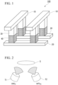
- This structure has a form in which pairs of a selector portion and a memory portion are sandwiched between the top and bottom electrode wirings as shown in FIG. 1 .
- the memory portion exhibits non-volatile resistance changes and is formed of, for example, a material composed of Ge-Sb-Te.
- the selector portion has a role of designating memory portions that perform writing and reading and has been formed of a As-Se-Ge-Si-based amorphous material in the related art.
- OTS ovonic threshold switching
- Patent Document 1 proposes a tertiary or quaternary OTS material containing at least one element of As, Se and Pb as a material for selectors. All of As, Se and Pb cause a high environmental load and are toxic repellent elements, which is a problem.
- Patent Document 2 discloses that a tellurium-containing compound layer as a selector contains at least one M1 element selected from Sn, Cu and Bi, Te and O.
- M1 element does not include Hf, and the details of an electrical resistance change thereof are unclear.
- Patent Document 3 describes that at least one chalcogen element selected from Te, Se and S is contained as a material for selectors, but the environmental load is high in a case where Se is used.
- Non-Patent Document 1 the fact that an X-Zn-Te (X: Be, Mg or Ca)-based material composed of Zn and Te has substantially no higher threshold voltage V th than practical OTS materials is theoretically shown by the first-principles calculation, which is merely a study showing only prediction by the first-principles calculation, and no actual electrical resistance changes are described.
- X-Zn-Te X: Be, Mg or Ca
- Non-Patent Document 2 shows the OTS characteristics of a Si-Ge-As-Te-based amorphous material composed of Si, Ge, As and Te, but As is contained, and the environmental load is high.
- Non-Patent Document 3 shows HfTesOs, which is a Hf-Te-O-based compound, as a crystal material not as an amorphous material, but whether or not the material has characteristics enabling the material to be used as selectors in cross-point type memories is not disclosed.
- an object of the present invention is to provide a new material causing a low environmental load and having characteristics enabling the material to be used for selectors in cross-point type memories.
- a material according to a first aspect of the present invention is an amorphous material that contains Hf, O and Te as main components and has characteristics of an electrical resistance transitioning from a first state to a second state that is lower than the first state at a specific threshold voltage in a case where the applied voltage is increased.
- the electrical resistance transitions from the second state to the first state at a specific voltage in a case where the applied voltage is unloaded.
- a material according to a second aspect of the present invention is an amorphous material that contains Hf, O and Te as main components and is for a selector in a cross-point type memory.
- the amorphous material according to the aspect is represented by a general formula Hf x Te y O 100-x-y ⁇ (1), and in the formula (1), x and y may be 23.0 ⁇ x ⁇ 32.0, 10.0 ⁇ y ⁇ 22.0 and 35 ⁇ x + y ⁇ 50.
- x and y may be 23.0 ⁇ x ⁇ 30.0 and 13.0 ⁇ y ⁇ 22.0.
- x and y may be 23.0 ⁇ x ⁇ 28.0 and 15.0 ⁇ y ⁇ 22.0.
- a cross-point type memory has a first electrode wiring, a second electrode wiring, a memory portion and a selector portion containing the amorphous material according to the above-described aspect, and the memory portion and the selector portion are disposed between the first electrode wiring and the second electrode wiring.
- a material causing a low environmental load and having characteristics enabling the material to be used for selectors in cross-point type memories can be obtained.
- a material according to an embodiment of the present invention is an amorphous material containing Hf, O and Te and having threshold switch characteristics of the electrical resistance transitioning from a high state to a low state at a specific threshold voltage V th in a case where the applied voltage is increased.
- Such an amorphous material is used as a selector in a cross-point type memory and exhibits an abrupt resistance change from an off state where the electrical resistance is high to an on state where the electrical resistance is low when a voltage of the threshold voltage V th or higher is applied thereto. More specifically, in a case where the applied voltage is lower than the threshold voltage V th , the selector portion transitions to the off state, whereby a current toward the memory portion is cut off, and when the voltage applied to the selector portion becomes equal to or higher than the threshold voltage V th , the selector portion transitions to the on state, and a current is let to flow toward the memory portion through the selector portion.
- Such threshold switch characteristics of the selector portion are those of reversible and abrupt occurrence.
- the amorphous material according to the present embodiment changes from the on state where the electrical resistance is low to the off state where the electrical resistance is high or vice versa between amorphous and amorphous.
- the ratio of the electrical resistance in the off state where the electrical resistance is high to the electrical resistance in the on state where the electrical resistance is low is, for example, 10 times or more.
- the amorphous material containing Hf, O and Te preferably has a band gap Eg in a range of 1.0 eV ⁇ Eg ⁇ 1.5 eV in order to be used for selectors in cross-point type memories.
- Such a Eg range can be represented as described below as the range of the composition of the amorphous material containing Hf, O and Te. That is, there is a relationship represented by a general formula Hf x Te y O 100-x-y . . . (1) among Hf, O and Te, and in the formula (1), x (at.%) and y (at.%) are selected in ranges of 23.0 ⁇ x ⁇ 32.0 and 10.0 ⁇ y ⁇ 22.0 so that 35 (at.%) ⁇ x + y ⁇ 50 (at.%) is satisfied.
- the threshold voltage V th as the threshold switch characteristics is preferably in a range of 0.8 V ⁇ V th ⁇ 2.0 V
- x is in a range of 23.0 ⁇ x ⁇ 30.0 and y is in a range of 13.0 ⁇ y ⁇ 22.0.
- the threshold voltage V th as the threshold switch characteristics is more preferably in a range of 0.8 V ⁇ V th ⁇ 1.5 V
- x is in a range of 23.0 ⁇ x ⁇ 28.0 and y is in a range of 15.0 ⁇ y ⁇ 22.0.
- a cross-point type memory 100 is formed such that a plurality of pairs of a selector portion 30 and a memory portion 40 are sandwiched between the top and bottom electrode wirings, that is, between an electrode 10 and an electrode 20, as shown in FIG. 1 .
- the selector portion 30 is formed of the amorphous material described above.
- the selector portion 30 in order to form the selector portion 30, there is a need to perform sputtering using, for example, a first alloy target T1 composed of HfO 2 and a second alloy target T2 composed of HfTe 2 and form films thereof on a substrate S composed of Si or glass.
- a first alloy target T1 composed of HfO 2
- a second alloy target T2 composed of HfTe 2 and form films thereof on a substrate S composed of Si or glass.
- the composition of Hf, Te and O is adjusted to be within a composition range where the amorphous material has the threshold switch characteristics by controlling the target output in the sputtering of two materials having extremely different band gaps Eg.
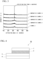
- FIG. 2 is a view for describing a film formation step of a Hf-Te-O film.
- Hf-Te-O films were formed on a SiO 2 /Si substrate and a sapphire substrate by the RF magnetron sputtering method at room temperature.
- a plurality of thin film specimens having different compositions were produced using a HfOz alloy target and a HfTe 2 alloy target by controlling the output ratio for each and regarded as Example 1 and Comparative Example 1 to Comparative Example 4.
- Example 1 and Comparative Example 1 to Comparative Example 4 there are a specimen having a Hf-Te-O film formed on a SiO 2 /Si substrate and a specimen having a Hf-Te-O film formed on a sapphire substrate for convenience.
- the Hf-Te-O films formed in each of the example and the comparative examples are considered to have the same characteristics regardless of the type of the substrate.
- compositions of the specimens of Example 1 and Comparative Example 1 to Comparative Example 4 produced on the SiO 2 /Si substrates in an off state were measured by the Rutherford backscattering spectrometry.
- the Rutherford backscattering spectrometry was performed under the following conditions.
- Incident ion 4 He ++ , incident energy: 2300 keV, incident angle: 0°, scattering angle: 160°, specimen current: 18 nA, beam diameter: 2 mm ⁇ , in-plane rotation: none, irradiation quantity: 150 ⁇ C
- Example 1 The compositions obtained regarding Example 1 and Comparative Example 1 to Comparative Example 4 are as shown in Table 1 below.
- Table 1 Hf (at.%) Te (at.%) O (at.%) Eg (eV)
- Example 1 24 21 55 1.0 Comparative Example 1 34 0 66 5.0 Comparative Example 2 32 10 58 1.5 Comparative Example 3 16 29 55 0.52 Comparative Example 4 14 44 42 0.46
- FIG. 3 is a view showing the measurement results of the example and the comparative examples by the X-ray diffraction method.
- the vertical axis represents the intensity in an arbitrary unit
- the horizontal axis represents the diffraction angle 2 ⁇ (degrees).
- reflection peaks from the Si substrates are shown. It is found that all patterns do not have any clear peaks except peaks derived from the Si substrates and amorphous phases are exhibited.
- FIG. 4 is a cross-sectional view of an element 50 for evaluating the threshold switch characteristics.
- a 65 nm-thick TiN/W film was formed on a SiO 2 /Si substrate 4 as a lower electrode 3, and a 100 nm-thick Hf-Te-O film 2 was formed in a state of coating a part of the lower electrode 3.
- the purpose of forming this Hf-Te-O film 2 in a state of coating a part of the lower electrode 3 is to expose the part of the lower electrode 3.
- elements having the Hf-Te-O film 2 formed under the conditions of Example 1 and elements having the Hf-Te-O film 2 formed under the conditions of Comparative Example 1 were prepared.
- FIG. 5 shows the I-V characteristics of Comparative Example 1.
- a high resistance state was shown in the low-voltage region, and an abrupt current increase was confirmed at approximately 11 V, but the state did not return to high resistance and remained in a low resistance state after the voltage was unloaded. This resistance change is attributed to breakdown and is irreversible. From this fact, it is found that, in the case of a material having a large band gap Eg as in Comparative Example 1, the threshold switch characteristics are not shown and the element does not function as a selector portion.
- the maximum value of the applied voltage is set to 15 V, and currents in a process of increasing the voltage from 0 V to 15 V and a process of unloading the voltage from 15 V to 0 V are measured.
- the compliance current is set to 1 mA to prevent the elements from breaking due to an abrupt increase in current.
- the element also did not have threshold switch characteristics in Comparative Example 2, which will not be described in detail.
- Example 1 On the other hand, from the I-V characteristics of Example 1 shown in FIG. 6 , the threshold switch characteristics were confirmed. When the voltage was low in the voltage increase process, only several micro amperes to several tens of micro amperes flowed, and a high resistance was shown. At approximately 0.8 V, an abrupt increase in current was shown, the resistance was lowered, and the compliance current value of 1 mA was reached. After that, when approximately 0.6 V was reached in the voltage unload process, an abrupt decrease in current was confirmed, a high resistance state was shown again, and the voltage characteristics were confirmed to be reversible. These results demonstrate that the threshold switch characteristics were shown in Example 1 and indicate that the element can be used as a selector portion.
- FIG. 7 is a view showing the I-V characteristics of a case where the band gap Eg is 1.0 eV in a numerical simulation and Example 1. As shown in FIG. 7 , the I-V characteristics of Example 1 can be almost reproduced in the numerical simulation. Results with the band gap Eg changed in the numerical simulation are shown in FIG. 8 and FIG. 9 .
- FIG. 8 is a view showing the I-V characteristics in the numerical simulation. FIG. 8 shows the I-V characteristics in cases where Eg is 1.0 eV, 1.1 eV, 1.2 eV, 1.3 eV and 1.4 eV In FIG. 8 , it is shown that the element has the threshold switch characteristics with respect to all of the above-listed band gaps. On the other hand, FIG.
- the threshold voltage V th with respect to the band gap Eg.
- the threshold voltage V th is preferably as low as possible, however, when the threshold voltage V th becomes lower than 0.8 V that corresponds to a band gap Eg of 1.0 eV, the resistance of the element becomes too small, which is not preferable.
- the threshold voltage V th that corresponds to a band gap Eg of 1.4 eV is approximately 2.4 V, which is lower than the upper limit (2.7 V) of the threshold voltage V th of typical OTS materials.
- the threshold voltage V th is preferably as low as possible, when the threshold voltage V th is set to 2.0 V or lower, the band gap Eg is in a range of approximately 1.3 eV or smaller in the present numerical simulation. In addition, when the threshold voltage V th is set to 1.5 V or lower, the band gap Eg is in a range of approximately 1.2 eV or smaller in the present numerical simulation. In addition, the range of the atomic weight ratio of Hf, Te and O can also be calculated according to the above-described range of the threshold voltage.
Landscapes
- Engineering & Computer Science (AREA)
- Chemical & Material Sciences (AREA)
- Materials Engineering (AREA)
- Manufacturing & Machinery (AREA)
- Semiconductor Memories (AREA)
Abstract
Description
- The present invention relates to an amorphous material that can be used for, for example, selectors in cross-point type memories and a cross-point type memory.
- Cross-point type memories have a structure capable of realizing a high degree of integration and have already been employed as commercially available non-volatile memories. This structure has a form in which pairs of a selector portion and a memory portion are sandwiched between the top and bottom electrode wirings as shown in
FIG. 1 . The memory portion exhibits non-volatile resistance changes and is formed of, for example, a material composed of Ge-Sb-Te. On the other hand, the selector portion has a role of designating memory portions that perform writing and reading and has been formed of a As-Se-Ge-Si-based amorphous material in the related art. This is to realize ovonic threshold switching (OTS) with the non-linear I-V characteristics of amorphous chalcogenide materials. However, As-Se-Ge-Si-based OTS materials are toxic and contain As and Se which cause a high environmental load. - In addition,
Patent Document 1 proposes a tertiary or quaternary OTS material containing at least one element of As, Se and Pb as a material for selectors. All of As, Se and Pb cause a high environmental load and are toxic repellent elements, which is a problem. - Furthermore,
Patent Document 2 discloses that a tellurium-containing compound layer as a selector contains at least one M1 element selected from Sn, Cu and Bi, Te and O. However, the M1 element does not include Hf, and the details of an electrical resistance change thereof are unclear. - In addition,
Patent Document 3 describes that at least one chalcogen element selected from Te, Se and S is contained as a material for selectors, but the environmental load is high in a case where Se is used. - Furthermore, in
Non-Patent Document 1, the fact that an X-Zn-Te (X: Be, Mg or Ca)-based material composed of Zn and Te has substantially no higher threshold voltage Vth than practical OTS materials is theoretically shown by the first-principles calculation, which is merely a study showing only prediction by the first-principles calculation, and no actual electrical resistance changes are described. - In addition, Non-Patent
Document 2 shows the OTS characteristics of a Si-Ge-As-Te-based amorphous material composed of Si, Ge, As and Te, but As is contained, and the environmental load is high. -
Non-Patent Document 3 shows HfTesOs, which is a Hf-Te-O-based compound, as a crystal material not as an amorphous material, but whether or not the material has characteristics enabling the material to be used as selectors in cross-point type memories is not disclosed. -
- [Patent Document 1]
Japanese Unexamined Patent Application, First Publication No. 2018-198321 - [Patent Document 2]
Japanese Unexamined Patent Application, First Publication No. 2021-48258 - [Patent Document 3]
Japanese Patent No. 6613142 -
- [Non-Patent Document 1]
Yun-Jae Lee, Minwoo Han, Su-Hyun Yoo, and Aloysius Soon, "Tunable Threshold Voltage of ZnTe-Based Ovonic Switching Devices via Isovalent Cation Exchange", ACS Applied Electronic Materials 3, 1107-1114 (2021). - [Non-Patent Document 2]
D. Garbin, W. Devulder, R. Degraeve, G. L. Donadio, S. Clima, K. Opsomer, A. Fantini, D. Cellier, W. G. Kim, M. Pakala, A. Cockbum, C. Detavernier, R. Delhougne, L. Goux, G. S. Kar, "Composition Optimization and Device Understanding of Si-Ge-As-Te Ovonic Threshold Switch Selector with Excellent Endurance", Proceedings of 2019 Int. Electron Devices Meeting (IEDM) 35.1.1-35.1.4 - [Non-Patent Document 3]
J. Galy, G. Meunier, "Sur de nouveaux composes de formule MTesOs (M= Ti, Zr, Hf, Sn) de structure fluorine deformee", Comptes Rendus des Seances de l'Academic des Sciences, Serie C: Sciences Chimiques 268 1249-1252 (1969). - Therefore, according to one aspect, an object of the present invention is to provide a new material causing a low environmental load and having characteristics enabling the material to be used for selectors in cross-point type memories.
- A material according to a first aspect of the present invention is an amorphous material that contains Hf, O and Te as main components and has characteristics of an electrical resistance transitioning from a first state to a second state that is lower than the first state at a specific threshold voltage in a case where the applied voltage is increased.
- In addition, in the material according to the aspect, the electrical resistance transitions from the second state to the first state at a specific voltage in a case where the applied voltage is unloaded.
- In addition, a material according to a second aspect of the present invention is an amorphous material that contains Hf, O and Te as main components and is for a selector in a cross-point type memory.
- In addition, the amorphous material according to the aspect is represented by a general formula HfxTeyO100-x-y ··· (1), and in the formula (1), x and y may be 23.0 < x < 32.0, 10.0 < y < 22.0 and 35 ≤ x + y ≤ 50.
- In addition, in the formula (1), x and y may be 23.0 < x < 30.0 and 13.0 < y < 22.0.
- In addition, in the formula (1), x and y may be 23.0 < x < 28.0 and 15.0 < y < 22.0.
- A cross-point type memory according to one aspect of the present invention has a first electrode wiring, a second electrode wiring, a memory portion and a selector portion containing the amorphous material according to the above-described aspect, and the memory portion and the selector portion are disposed between the first electrode wiring and the second electrode wiring.
- According to one aspect, a material causing a low environmental load and having characteristics enabling the material to be used for selectors in cross-point type memories can be obtained.
-
-
FIG. 1 is a view showing a structural example of a cross-point type memory. -
FIG. 2 is a view schematically showing a film formation step of a Hf-Te-O film. -
FIG. 3 is a view showing measurement results of an example and comparative examples by an X-ray diffraction method. -
FIG. 4 is a cross-sectional view of an element for evaluating threshold switch characteristics. -
FIG. 5 is a view showing the I-V characteristics of Comparative Example 1. -
FIG. 6 is a view showing the I-V characteristics of Example 1. -
FIG. 7 is a view showing the I-V characteristics of a case where the band gap Eg is 1.0 eV in a numerical simulation and Example 1. -
FIG. 8 is a view showing the I-V characteristics in the numerical simulation. -
FIG. 9 is a view indicating a relationship between the band gap Eg and the threshold voltage Vth in the numerical simulation. - A material according to an embodiment of the present invention is an amorphous material containing Hf, O and Te and having threshold switch characteristics of the electrical resistance transitioning from a high state to a low state at a specific threshold voltage Vth in a case where the applied voltage is increased.
- Such an amorphous material is used as a selector in a cross-point type memory and exhibits an abrupt resistance change from an off state where the electrical resistance is high to an on state where the electrical resistance is low when a voltage of the threshold voltage Vth or higher is applied thereto. More specifically, in a case where the applied voltage is lower than the threshold voltage Vth, the selector portion transitions to the off state, whereby a current toward the memory portion is cut off, and when the voltage applied to the selector portion becomes equal to or higher than the threshold voltage Vth, the selector portion transitions to the on state, and a current is let to flow toward the memory portion through the selector portion. Such threshold switch characteristics of the selector portion are those of reversible and abrupt occurrence.
- The amorphous material according to the present embodiment changes from the on state where the electrical resistance is low to the off state where the electrical resistance is high or vice versa between amorphous and amorphous. The ratio of the electrical resistance in the off state where the electrical resistance is high to the electrical resistance in the on state where the electrical resistance is low is, for example, 10 times or more.
- The present inventors non-obviously found that the amorphous material containing Hf, O and Te preferably has a band gap Eg in a range of 1.0 eV ≤ Eg ≤ 1.5 eV in order to be used for selectors in cross-point type memories.
- Such a Eg range can be represented as described below as the range of the composition of the amorphous material containing Hf, O and Te. That is, there is a relationship represented by a general formula HfxTeyO100-x-y . . . (1) among Hf, O and Te, and in the formula (1), x (at.%) and y (at.%) are selected in ranges of 23.0 < x < 32.0 and 10.0 < y < 22.0 so that 35 (at.%) ≤ x + y ≤ 50 (at.%) is satisfied.
- Furthermore, the threshold voltage Vth as the threshold switch characteristics is preferably in a range of 0.8 V ≤ Vth ≤ 2.0 V Such a condition corresponds to the fact that, in the formula (1), x is in a range of 23.0 < x < 30.0 and y is in a range of 13.0 < y < 22.0.
- Furthermore, the threshold voltage Vth as the threshold switch characteristics is more preferably in a range of 0.8 V ≤ Vth ≤ 1.5 V Such a condition corresponds to the fact that, in the formula (1), x is in a range of 23.0 < x < 28.0 and y is in a range of 15.0 < y < 22.0.
- A
cross-point type memory 100 is formed such that a plurality of pairs of aselector portion 30 and amemory portion 40 are sandwiched between the top and bottom electrode wirings, that is, between anelectrode 10 and anelectrode 20, as shown inFIG. 1 . Theselector portion 30 is formed of the amorphous material described above. Theselector portion 30 is formed by, for example, forming films of HfO2 (Eg = 5.6 eV), which is an insulator and has a large band gap Eg, and HfTe2 (Eg = 0 eV), which is a semimetal, by sputtering at the same time. That is, in order to form theselector portion 30, there is a need to perform sputtering using, for example, a first alloy target T1 composed of HfO2 and a second alloy target T2 composed of HfTe2 and form films thereof on a substrate S composed of Si or glass. As described above, the composition of Hf, Te and O is adjusted to be within a composition range where the amorphous material has the threshold switch characteristics by controlling the target output in the sputtering of two materials having extremely different band gaps Eg. - Hereinafter, the present invention will be described in more detail by showing examples, but the present invention is not limited to these examples by any means.
-
FIG. 2 is a view for describing a film formation step of a Hf-Te-O film. As schematically shown inFIG. 2 , Hf-Te-O films were formed on a SiO2/Si substrate and a sapphire substrate by the RF magnetron sputtering method at room temperature. Here, a plurality of thin film specimens having different compositions were produced using a HfOz alloy target and a HfTe2 alloy target by controlling the output ratio for each and regarded as Example 1 and Comparative Example 1 to Comparative Example 4. Here, as described above, for each of Example 1 and Comparative Example 1 to Comparative Example 4, there are a specimen having a Hf-Te-O film formed on a SiO2/Si substrate and a specimen having a Hf-Te-O film formed on a sapphire substrate for convenience. However, the Hf-Te-O films formed in each of the example and the comparative examples are considered to have the same characteristics regardless of the type of the substrate. - The compositions of the specimens of Example 1 and Comparative Example 1 to Comparative Example 4 produced on the SiO2/Si substrates in an off state were measured by the Rutherford backscattering spectrometry. The Rutherford backscattering spectrometry was performed under the following conditions.
- Incident ion: 4He++, incident energy: 2300 keV, incident angle: 0°, scattering angle: 160°, specimen current: 18 nA, beam diameter: 2 mmφ, in-plane rotation: none, irradiation quantity: 150 µC
- The compositions obtained regarding Example 1 and Comparative Example 1 to Comparative Example 4 are as shown in Table 1 below.
[Table 1] Hf (at.%) Te (at.%) O (at.%) Eg (eV) Example 1 24 21 55 1.0 Comparative Example 1 34 0 66 5.0 Comparative Example 2 32 10 58 1.5 Comparative Example 3 16 29 55 0.52 Comparative Example 4 14 44 42 0.46 - In addition, it was confirmed by an X-ray diffraction method that all of the specimens of Example 1 and Comparative Example 1 to Comparative Example 4 produced on the SiO2/Si substrates exhibited an amorphous phase. This is shown in
FIG. 3. FIG. 3 is a view showing the measurement results of the example and the comparative examples by the X-ray diffraction method. InFIG. 3 , the vertical axis represents the intensity in an arbitrary unit, and the horizontal axis represents the diffraction angle 2θ (degrees). InFIG. 3 , reflection peaks from the Si substrates are shown. It is found that all patterns do not have any clear peaks except peaks derived from the Si substrates and amorphous phases are exhibited. - Regarding the Hf-Te-O films formed on the sapphire substrates, transmittance spectra were measured, and absorption coefficients were calculated from the obtained results. A Tauc plot was performed based on the obtained absorption coefficients, the band gap Eg of each sample was estimated, and the results shown in Table 1 were obtained. As described above, it is found that, in Comparative Examples 1 to 4, the band gaps Eg are 0.52 or smaller or 1.5 or larger. On the other hand, it was confirmed that the value of the band gap Eg of Example 1 is between 0.52 and 1.5.
- Elements as shown in
FIG. 4 were produced to evaluate the threshold switch characteristics of the Hf-Te-O films.FIG. 4 is a cross-sectional view of anelement 50 for evaluating the threshold switch characteristics. In order to produce theelement 50, first, a 65 nm-thick TiN/W film was formed on a SiO2/Si substrate 4 as alower electrode 3, and a 100 nm-thick Hf-Te-O film 2 was formed in a state of coating a part of thelower electrode 3. The purpose of forming this Hf-Te-O film 2 in a state of coating a part of thelower electrode 3 is to expose the part of thelower electrode 3. After that, a resist pattern was formed using photolithography, and a 115 nm-thick W/TiN film was formed as anupper electrode 1. Finally, the resist was removed by lift-off. As the elements, two types of elements were prepared: elements produced by forming the Hf-Te-O film 2 under the same conditions as in Example 1 and elements produced by forming the Hf-Te-O film 2 under the same conditions as in Comparative Example 1. - As the
element 50 for evaluating the threshold switch characteristics, elements having the Hf-Te-O film 2 formed under the conditions of Example 1 and elements having the Hf-Te-O film 2 formed under the conditions of Comparative Example 1 were prepared. - A DC voltage was applied from the
upper electrode 1 toward thelower electrode 3 of the element shown inFIG. 4 , and a flowing current was measured, thereby evaluating the I (current)-V (voltage) characteristics.FIG. 5 shows the I-V characteristics of Comparative Example 1. A high resistance state was shown in the low-voltage region, and an abrupt current increase was confirmed at approximately 11 V, but the state did not return to high resistance and remained in a low resistance state after the voltage was unloaded. This resistance change is attributed to breakdown and is irreversible. From this fact, it is found that, in the case of a material having a large band gap Eg as in Comparative Example 1, the threshold switch characteristics are not shown and the element does not function as a selector portion. The maximum value of the applied voltage is set to 15 V, and currents in a process of increasing the voltage from 0 V to 15 V and a process of unloading the voltage from 15 V to 0 V are measured. In addition, the compliance current is set to 1 mA to prevent the elements from breaking due to an abrupt increase in current. In addition, the element also did not have threshold switch characteristics in Comparative Example 2, which will not be described in detail. - On the other hand, from the I-V characteristics of Example 1 shown in
FIG. 6 , the threshold switch characteristics were confirmed. When the voltage was low in the voltage increase process, only several micro amperes to several tens of micro amperes flowed, and a high resistance was shown. At approximately 0.8 V, an abrupt increase in current was shown, the resistance was lowered, and the compliance current value of 1 mA was reached. After that, when approximately 0.6 V was reached in the voltage unload process, an abrupt decrease in current was confirmed, a high resistance state was shown again, and the voltage characteristics were confirmed to be reversible. These results demonstrate that the threshold switch characteristics were shown in Example 1 and indicate that the element can be used as a selector portion. - From these results, there is a demand for the band gap Eg to be in an appropriate range since the threshold switch characteristics cannot be obtained when the band gap Eg is too large. On the other hand, it was confirmed by a simulation, which will be described below, that, when the band gap Eg decreases to the values of Comparative Examples 3 and 4, the electrical resistance of the element becomes too low, and the off state is not shown.
-
FIG. 7 is a view showing the I-V characteristics of a case where the band gap Eg is 1.0 eV in a numerical simulation and Example 1. As shown inFIG. 7 , the I-V characteristics of Example 1 can be almost reproduced in the numerical simulation. Results with the band gap Eg changed in the numerical simulation are shown inFIG. 8 andFIG. 9 .FIG. 8 is a view showing the I-V characteristics in the numerical simulation.FIG. 8 shows the I-V characteristics in cases where Eg is 1.0 eV, 1.1 eV, 1.2 eV, 1.3 eV and 1.4 eV InFIG. 8 , it is shown that the element has the threshold switch characteristics with respect to all of the above-listed band gaps. On the other hand,FIG. 9 shows the threshold voltage Vth with respect to the band gap Eg. InFIG. 9 , a threshold voltage Vth at each of the band gaps Eg = 1.0 eV to 1.4 eV is shown. The threshold voltage Vth is preferably as low as possible, however, when the threshold voltage Vth becomes lower than 0.8 V that corresponds to a band gap Eg of 1.0 eV, the resistance of the element becomes too small, which is not preferable. Incidentally, in the present numerical simulation, the threshold voltage Vth that corresponds to a band gap Eg of 1.4 eV is approximately 2.4 V, which is lower than the upper limit (2.7 V) of the threshold voltage Vth of typical OTS materials. Since the threshold voltage Vth is preferably as low as possible, when the threshold voltage Vth is set to 2.0 V or lower, the band gap Eg is in a range of approximately 1.3 eV or smaller in the present numerical simulation. In addition, when the threshold voltage Vth is set to 1.5 V or lower, the band gap Eg is in a range of approximately 1.2 eV or smaller in the present numerical simulation. In addition, the range of the atomic weight ratio of Hf, Te and O can also be calculated according to the above-described range of the threshold voltage. -
- 1, 3 Electrode
- 2 Hf-Te-O film
- 4 Substrate
- 10 Electrode (writing electrode)
- 20 Electrode (reading electrode)
- 30 Selector portion
- 40 Memory portion
- 50 Threshold switch
- 100 Cross-point type memory
Claims (6)
- An amorphous material thatcontains Hf, O and Te as main components andhas characteristics of an electrical resistance transitioning from a first state to a second state that is lower than the first state at a specific threshold voltage.
- An amorphous material that contains Hf, O and Te as main components and is for a selector in a cross-point type memory.
- The amorphous material according to Claim 1 or 2,wherein the amorphous material is represented by a general formula HfxTeyO100-x-y ··· (1), andin the formula (1), 23.0 < x < 32.0, 10.0 < y < 22.0 and 35 ≤ x + y ≤ 50.
- The amorphous material according to Claim 3,
wherein, in the formula (1), 23.0 < x < 30.0 and 13.0 < y < 22.0. - The amorphous material according to Claim 3,
wherein, in the formula (1), 23.0 < x < 28.0 and 15.0 < y < 22.0. - A cross-point type memory comprising:a first electrode wiring;a second electrode wiring;a memory portion; anda selector portion containing the amorphous material according to any one of Claims 1 to 5,wherein the memory portion and the selector portion are disposed between the first electrode wiring and the second electrode wiring.
Applications Claiming Priority (2)
| Application Number | Priority Date | Filing Date | Title |
|---|---|---|---|
| JP2021175169 | 2021-10-27 | ||
| PCT/JP2022/039485 WO2023074609A1 (en) | 2021-10-27 | 2022-10-24 | Amorphous material and cross-point type memory |
Publications (2)
| Publication Number | Publication Date |
|---|---|
| EP4426083A1 true EP4426083A1 (en) | 2024-09-04 |
| EP4426083A4 EP4426083A4 (en) | 2025-11-12 |
Family
ID=86159921
Family Applications (1)
| Application Number | Title | Priority Date | Filing Date |
|---|---|---|---|
| EP22886936.8A Pending EP4426083A4 (en) | 2021-10-27 | 2022-10-24 | Amorphous Material and Crosspoint Storage |
Country Status (6)
| Country | Link |
|---|---|
| US (1) | US20250008744A1 (en) |
| EP (1) | EP4426083A4 (en) |
| JP (1) | JP7789400B2 (en) |
| KR (1) | KR102855972B1 (en) |
| TW (1) | TWI832515B (en) |
| WO (1) | WO2023074609A1 (en) |
Family Cites Families (10)
| Publication number | Priority date | Publication date | Assignee | Title |
|---|---|---|---|---|
| CN104871314B (en) * | 2012-12-25 | 2019-03-08 | 索尼半导体解决方案公司 | Storage elements and storage devices |
| JP6151650B2 (en) * | 2014-01-17 | 2017-06-21 | ソニーセミコンダクタソリューションズ株式会社 | Storage device |
| WO2015107945A1 (en) * | 2014-01-17 | 2015-07-23 | ソニー株式会社 | Switch element and memory device |
| US9806129B2 (en) | 2014-02-25 | 2017-10-31 | Micron Technology, Inc. | Cross-point memory and methods for fabrication of same |
| JP6791845B2 (en) * | 2015-03-31 | 2020-11-25 | ソニーセミコンダクタソリューションズ株式会社 | Switch element and storage device |
| JP2019129239A (en) * | 2018-01-25 | 2019-08-01 | ソニーセミコンダクタソリューションズ株式会社 | Storage element and storage device |
| JP7145495B2 (en) * | 2018-10-15 | 2022-10-03 | 国立研究開発法人産業技術総合研究所 | nonvolatile memory element |
| JP2021048258A (en) | 2019-09-18 | 2021-03-25 | キオクシア株式会社 | Resistance change element |
| JP7433973B2 (en) * | 2020-02-20 | 2024-02-20 | キオクシア株式会社 | Nonvolatile semiconductor memory device and its manufacturing method |
| JP2021136301A (en) * | 2020-02-26 | 2021-09-13 | キオクシア株式会社 | Nonvolatile semiconductor memory device and method for manufacturing the same |
-
2022
- 2022-10-24 US US18/704,390 patent/US20250008744A1/en active Pending
- 2022-10-24 EP EP22886936.8A patent/EP4426083A4/en active Pending
- 2022-10-24 WO PCT/JP2022/039485 patent/WO2023074609A1/en not_active Ceased
- 2022-10-24 KR KR1020247012039A patent/KR102855972B1/en active Active
- 2022-10-24 JP JP2023556417A patent/JP7789400B2/en active Active
- 2022-10-26 TW TW111140533A patent/TWI832515B/en active
Also Published As
| Publication number | Publication date |
|---|---|
| JPWO2023074609A1 (en) | 2023-05-04 |
| US20250008744A1 (en) | 2025-01-02 |
| TWI832515B (en) | 2024-02-11 |
| JP7789400B2 (en) | 2025-12-22 |
| WO2023074609A1 (en) | 2023-05-04 |
| EP4426083A4 (en) | 2025-11-12 |
| KR102855972B1 (en) | 2025-09-04 |
| TW202330392A (en) | 2023-08-01 |
| KR20240056754A (en) | 2024-04-30 |
Similar Documents
| Publication | Publication Date | Title |
|---|---|---|
| Shen et al. | Thermal barrier phase change memory | |
| US10991882B2 (en) | Methods of forming resistive memory elements | |
| CN110165048B (en) | Transition metal oxide resistive switching device with doped buffer | |
| DE102004052647B4 (en) | Method for improving the thermal properties of semiconductor memory cells in the manufacturing process and non-volatile, resistively switching memory cell | |
| US20030047765A1 (en) | Stoichiometry for chalcogenide glasses useful for memory devices and method of formation | |
| US8598560B1 (en) | Resistive memory elements exhibiting increased interfacial adhesion strength, methods of forming the same, and related resistive memory cells and memory devices | |
| US7884342B2 (en) | Phase change memory bridge cell | |
| Gu et al. | Conductive path formation in the Ta2O5 atomic switch: first-principles analyses | |
| Hatayama et al. | Low resistance-drift characteristics in Cr2Ge2Te6-based phase change memory devices with a high-resistance crystalline phase | |
| Dai et al. | Forming free and ultralow-power erase operation in atomically crystal TiO2 resistive switching | |
| KR20200073165A (en) | Nonvolatile resistance change memory using lead-free halide perovskite material | |
| Aziz et al. | Improved memory performance of ALD grown HfO2 films by nitrogen doping | |
| Cohen et al. | Low RESET Current Mushroom‐Cell Phase‐Change Memory Using Fiber‐Textured Homostructure GeSbTe on Highly Oriented Seed Layer | |
| KR20180057977A (en) | Memory device having chalcogenide composite selection device | |
| Kim et al. | Thickness dependence of resistive switching characteristics of the sol–gel processed Y2O3 RRAM devices | |
| Cojocaru-Mirédin et al. | Thermally Assisted Atomic-Scale Intermixing and Ordering in GeTe–Sb2Te3 Superlattices | |
| KR20240141705A (en) | Resistance change material, material for switch element, switch layer, switch element and memory device | |
| US20250008744A1 (en) | Amorphous material and cross-point type memory | |
| US11963459B2 (en) | Switching device and resistance variable device | |
| Guo et al. | The improved resistive switching of HfO2: Cu film with multilevel storage | |
| Shih et al. | Roles of oxygen and nitrogen in control of nonlinear resistive behaviors via filamentary and homogeneous switching in an oxynitride thin film memristor | |
| KR20240080367A (en) | Chalcogenide material and semiconductor device | |
| TW202606561A (en) | Amorphous material, selector element, production method for amorphous material, and production method for selector element | |
| Goux et al. | Self-limited filament formation and low-power resistive switching in CuxTe1-x/Al2O3/Si CBRAM cell | |
| US11600772B2 (en) | Resistance variable device with chalcogen-containing layer |
Legal Events
| Date | Code | Title | Description |
|---|---|---|---|
| STAA | Information on the status of an ep patent application or granted ep patent |
Free format text: STATUS: THE INTERNATIONAL PUBLICATION HAS BEEN MADE |
|
| PUAI | Public reference made under article 153(3) epc to a published international application that has entered the european phase |
Free format text: ORIGINAL CODE: 0009012 |
|
| STAA | Information on the status of an ep patent application or granted ep patent |
Free format text: STATUS: REQUEST FOR EXAMINATION WAS MADE |
|
| 17P | Request for examination filed |
Effective date: 20240424 |
|
| AK | Designated contracting states |
Kind code of ref document: A1 Designated state(s): AL AT BE BG CH CY CZ DE DK EE ES FI FR GB GR HR HU IE IS IT LI LT LU LV MC ME MK MT NL NO PL PT RO RS SE SI SK SM TR |
|
| DAV | Request for validation of the european patent (deleted) | ||
| DAX | Request for extension of the european patent (deleted) | ||
| A4 | Supplementary search report drawn up and despatched |
Effective date: 20251010 |
|
| RIC1 | Information provided on ipc code assigned before grant |
Ipc: H10B 63/10 20230101AFI20251006BHEP Ipc: H10B 63/00 20230101ALI20251006BHEP Ipc: H10N 70/00 20230101ALI20251006BHEP Ipc: H10N 99/00 20230101ALI20251006BHEP Ipc: H10N 70/20 20230101ALI20251006BHEP |