EP4425577A1 - Photoelectric conversion module, paddle, and method for manufacturing photoelectric conversion module - Google Patents
Photoelectric conversion module, paddle, and method for manufacturing photoelectric conversion module Download PDFInfo
- Publication number
- EP4425577A1 EP4425577A1 EP22886900.4A EP22886900A EP4425577A1 EP 4425577 A1 EP4425577 A1 EP 4425577A1 EP 22886900 A EP22886900 A EP 22886900A EP 4425577 A1 EP4425577 A1 EP 4425577A1
- Authority
- EP
- European Patent Office
- Prior art keywords
- photoelectric conversion
- conversion element
- connector
- connection portion
- conversion module
- Prior art date
- Legal status (The legal status is an assumption and is not a legal conclusion. Google has not performed a legal analysis and makes no representation as to the accuracy of the status listed.)
- Pending
Links
Images



Classifications
-
- B—PERFORMING OPERATIONS; TRANSPORTING
- B64—AIRCRAFT; AVIATION; COSMONAUTICS
- B64G—COSMONAUTICS; VEHICLES OR EQUIPMENT THEREFOR
- B64G1/00—Cosmonautic vehicles
- B64G1/22—Parts of, or equipment specially adapted for fitting in or to, cosmonautic vehicles
- B64G1/42—Arrangements or adaptations of power supply systems
- B64G1/44—Arrangements or adaptations of power supply systems using radiation, e.g. deployable solar arrays
- B64G1/443—Photovoltaic cell arrays
-
- H—ELECTRICITY
- H10—SEMICONDUCTOR DEVICES; ELECTRIC SOLID-STATE DEVICES NOT OTHERWISE PROVIDED FOR
- H10F—INORGANIC SEMICONDUCTOR DEVICES SENSITIVE TO INFRARED RADIATION, LIGHT, ELECTROMAGNETIC RADIATION OF SHORTER WAVELENGTH OR CORPUSCULAR RADIATION
- H10F19/00—Integrated devices, or assemblies of multiple devices, comprising at least one photovoltaic cell covered by group H10F10/00, e.g. photovoltaic modules
- H10F19/90—Structures for connecting between photovoltaic cells, e.g. interconnections or insulating spacers
- H10F19/902—Structures for connecting between photovoltaic cells, e.g. interconnections or insulating spacers for series or parallel connection of photovoltaic cells
- H10F19/904—Structures for connecting between photovoltaic cells, e.g. interconnections or insulating spacers for series or parallel connection of photovoltaic cells characterised by the shapes of the structures
-
- H—ELECTRICITY
- H10—SEMICONDUCTOR DEVICES; ELECTRIC SOLID-STATE DEVICES NOT OTHERWISE PROVIDED FOR
- H10F—INORGANIC SEMICONDUCTOR DEVICES SENSITIVE TO INFRARED RADIATION, LIGHT, ELECTROMAGNETIC RADIATION OF SHORTER WAVELENGTH OR CORPUSCULAR RADIATION
- H10F19/00—Integrated devices, or assemblies of multiple devices, comprising at least one photovoltaic cell covered by group H10F10/00, e.g. photovoltaic modules
- H10F19/30—Integrated devices, or assemblies of multiple devices, comprising at least one photovoltaic cell covered by group H10F10/00, e.g. photovoltaic modules comprising thin-film photovoltaic cells
-
- H—ELECTRICITY
- H10—SEMICONDUCTOR DEVICES; ELECTRIC SOLID-STATE DEVICES NOT OTHERWISE PROVIDED FOR
- H10F—INORGANIC SEMICONDUCTOR DEVICES SENSITIVE TO INFRARED RADIATION, LIGHT, ELECTROMAGNETIC RADIATION OF SHORTER WAVELENGTH OR CORPUSCULAR RADIATION
- H10F19/00—Integrated devices, or assemblies of multiple devices, comprising at least one photovoltaic cell covered by group H10F10/00, e.g. photovoltaic modules
- H10F19/40—Integrated devices, or assemblies of multiple devices, comprising at least one photovoltaic cell covered by group H10F10/00, e.g. photovoltaic modules comprising photovoltaic cells in a mechanically stacked configuration
-
- H—ELECTRICITY
- H10—SEMICONDUCTOR DEVICES; ELECTRIC SOLID-STATE DEVICES NOT OTHERWISE PROVIDED FOR
- H10F—INORGANIC SEMICONDUCTOR DEVICES SENSITIVE TO INFRARED RADIATION, LIGHT, ELECTROMAGNETIC RADIATION OF SHORTER WAVELENGTH OR CORPUSCULAR RADIATION
- H10F19/00—Integrated devices, or assemblies of multiple devices, comprising at least one photovoltaic cell covered by group H10F10/00, e.g. photovoltaic modules
- H10F19/90—Structures for connecting between photovoltaic cells, e.g. interconnections or insulating spacers
- H10F19/902—Structures for connecting between photovoltaic cells, e.g. interconnections or insulating spacers for series or parallel connection of photovoltaic cells
-
- H—ELECTRICITY
- H10—SEMICONDUCTOR DEVICES; ELECTRIC SOLID-STATE DEVICES NOT OTHERWISE PROVIDED FOR
- H10F—INORGANIC SEMICONDUCTOR DEVICES SENSITIVE TO INFRARED RADIATION, LIGHT, ELECTROMAGNETIC RADIATION OF SHORTER WAVELENGTH OR CORPUSCULAR RADIATION
- H10F71/00—Manufacture or treatment of devices covered by this subclass
-
- Y—GENERAL TAGGING OF NEW TECHNOLOGICAL DEVELOPMENTS; GENERAL TAGGING OF CROSS-SECTIONAL TECHNOLOGIES SPANNING OVER SEVERAL SECTIONS OF THE IPC; TECHNICAL SUBJECTS COVERED BY FORMER USPC CROSS-REFERENCE ART COLLECTIONS [XRACs] AND DIGESTS
- Y02—TECHNOLOGIES OR APPLICATIONS FOR MITIGATION OR ADAPTATION AGAINST CLIMATE CHANGE
- Y02E—REDUCTION OF GREENHOUSE GAS [GHG] EMISSIONS, RELATED TO ENERGY GENERATION, TRANSMISSION OR DISTRIBUTION
- Y02E10/00—Energy generation through renewable energy sources
- Y02E10/50—Photovoltaic [PV] energy
Definitions
- the present invention relates to a photoelectric conversion module, a paddle, and a method for manufacturing a photoelectric conversion module.
- Patent Literature 1 Photoelectric conversion modules that convert light energy into electrical energy are known (Patent Literature 1).
- the photoelectric conversion module described in Patent Literature 1 includes a plurality of photoelectric conversion elements. End portions of the photoelectric conversion elements adjacent to each other are overlapped with each other.
- the photoelectric conversion elements adjacent to each other are electrically connected to each other by a conductor such as solder in a region overlapping each other (see Fig. 5 of Patent Literature 1).
- Patent Literature 1 JP 2016-119401 A
- An overlapping region (non-power generation region) between photoelectric conversion elements adjacent to each other is preferably as narrow as possible.
- the overlapping region is narrow, the area of a conductor such as solder connecting the photoelectric conversion elements is reduced, and thus connection strength may be reduced.
- a load such as vibration applied to the mobile object may apply a large load to a connection portion between the photoelectric conversion elements.
- a photoelectric conversion module capable of connecting photoelectric conversion elements with stable connection strength and a method for manufacturing the photoelectric conversion module are desired.
- a photoelectric conversion module comprises: a first photoelectric conversion element; a second photoelectric conversion element; and a connector.
- the first photoelectric conversion element and the second photoelectric conversion element are arranged side by side so as to partially overlap each other.
- the connector is connected to the first photoelectric conversion element at a first connection portion.
- the connector is connected to the second photoelectric conversion element at a second connection portion away from the first connection portion.
- a method for manufacturing a photoelectric conversion module comprises: a step of preparing a first photoelectric conversion element, a second photoelectric conversion element, and a connector; a step of connecting the connector to the first photoelectric conversion element at a first connection portion; a step of arranging the first photoelectric conversion element and the second photoelectric conversion element side by side so as to partially overlap each other; and a step of connecting the connector to the second photoelectric conversion element at a second connection portion away from the first connection portion.
- a paddle according to one aspect comprises said photoelectric conversion module.
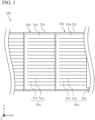
- Fig. 1 is a schematic plan view of a photoelectric conversion module according to a first embodiment.
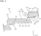
- Fig. 2 is a schematic side view of the photoelectric conversion module according to the first embodiment as viewed from a Y direction in Fig. 1 .
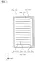
- Fig. 3 is a schematic plan view of each photoelectric conversion element constituting the photoelectric conversion module.
- Fig. 4 is a schematic plan view of a connector connecting photoelectric conversion modules adjacent to each other. Fig. 4 illustrates one surface of the connector facing a first photoelectric conversion element 10a described later.
- Fig. 5 is a schematic view for explaining a region of an insulator of the connector. Note that, in Fig. 3 , in order to describe the structure of each photoelectric conversion element constituting the photoelectric conversion module, reference numerals related to each photoelectric conversion element are attached.
- a photoelectric conversion module 100 includes a plurality of photoelectric conversion elements 10a and 10b, and a connector 200 that electrically connects the photoelectric conversion elements 10a and 10b adjacent to each other.
- the plurality of photoelectric conversion elements 10a and 10b is arranged side by side in one direction (X direction in the drawing).
- the photoelectric conversion elements 10a and 10b adjacent to each other are provided side by side so as to partially overlap each other. Specifically, one end portions of the photoelectric conversion elements 10a and 10b overlap the other end portions of the photoelectric conversion elements 10a and 10b adjacent thereto in a thickness direction.
- the photoelectric conversion elements 10a and 10b adjacent to each other are electrically connected to each other by the connector 200 in the overlapping portion.
- the number of photoelectric conversion elements 10a and 10b arranged in one direction may be at least two, and preferably three or more.
- the photoelectric conversion elements 10a and 10b according to the first embodiment may be thin-film photoelectric conversion elements.
- the photoelectric conversion elements 10a and 10b are solar cell elements that convert light energy into electrical energy.
- Each of the photoelectric conversion elements 10a and 10b has conductive substrates 20a and 20b serving as bases for forming respective layers such as first electrode layers 22a and 22b described later.
- the conductive substrates 20a and 20b are constructed by a substrate such as a metal substrate. Further, the conductive substrates 20a and 20b may be flexible substrates. The shapes and dimensions of the conductive substrates 20a and 20b are appropriately determined according to the sizes and the like of the photoelectric conversion elements 10a and 10b.
- the conductive substrates 20a and 20b are formed by, for example, titanium (Ti), stainless steel (SUS), copper or aluminum, or an alloy thereof, and so on.
- the conductive substrates 20a and 20b may have a laminated structure in which a plurality of metal base materials are laminated, and for example, a stainless foil, a titanium foil, or a molybdenum foil may be formed on the surface of the substrate.
- a metal material such as molybdenum, titanium, or chromium may be deposited on the back side of the conductive substrates 20a and 20b.
- the photoelectric conversion elements 10a and 10b can be bent, and cracking of the conductive substrates 20a and 20b can also be suppressed due to bending. Furthermore, in the above case, it is easy to reduce the weight and thickness of the photoelectric conversion module 100 as compared with a glass substrate.
- the photoelectric conversion elements 10a and 10b may include at least first electrode layers 22a and 22b, second electrode layers 24a and 24b, and photoelectric conversion layers 26a and 26b provided between the first electrode layers 22a and 22b and the second electrode layers 24a and 24b.
- the photoelectric conversion layers 26a and 26b are layers that contribute to mutual conversion of light energy and electric energy. In a solar cell element that converts light energy into electric energy, the photoelectric conversion layers 26a and 26b may be referred to as light absorption layers.
- the first electrode layers 22a and 22b and the second electrode layers 24a and 24b are adjacent to the photoelectric conversion layers 26a and 26b.
- adjacent shall mean not only that both layers are in direct contact, but also that both layers are in proximity via another layer.
- the first electrode layers 22a and 22b are provided between the photoelectric conversion layers 26a and 26b and the conductive substrates 20a and 20b.
- the second electrode layers 24a and 24b are located on the side opposite to the conductive substrates 20a and 20b with respect to the photoelectric conversion layers 26a and 26b. Therefore, the photoelectric conversion layers 26a and 26b are located between the first electrode layers 22a and 22b and the second electrode layers 24a and 24b.
- the first electrode layers 22a and 22b are connected to the conductive substrates 20a and 20b.
- the second electrode layers 24a and 24b may be constituted by transparent electrode layers.
- the second electrode layers 24a and 24b are formed by transparent electrode layers, light incident on the photoelectric conversion layers 26a and 26b or is emitted from the photoelectric conversion layers 26a and 26b passes through the second electrode layers 24a and 24b.
- the first electrode layers 22a and 22b may be formed by opaque electrode layers or may be formed of transparent electrode layers.
- the first electrode layers 22a and 22b may be formed by, for example, a metal such as molybdenum, titanium or chromium.
- the thickness of the first electrode layers 22a and 22b may be, for example, 50 nm to 1500 nm.
- the second electrode layers 24a and 24b may be formed by an n-type semiconductor, more specifically, a material having n-type conductivity and relatively low resistance.
- the second electrode layers 24a and 24b can also function as an n-type semiconductor and a transparent electrode layer.
- the second electrode layers 24a and 24b include, for example, a metal oxide to which a group III element (B, Al, Ga, or In) is added as a dopant. Examples of the metal oxide include ZnO and SnO 2 .
- the second electrode layer 24 can be selected from, for example, indium tin oxide (In 2 O 3 :Sn), indium titanium oxide (In 2 O 3 :Ti), indium zinc oxide (In 2 O 3 :Zn), tin zinc-doped indium oxide (In 2 O 3 :Sn, Zn), tungsten-doped indium oxide (In 2 O 3 :W), hydrogen-doped indium oxide (In 2 O 3 :H), indium gallium zinc oxide (InGaZnO 4 ), zinc tin oxide (ZnO:Sn), fluorine-doped tin oxide (SnO 2 :F), gallium-doped zinc oxide (ZnO:Ga), boron-doped zinc oxide (ZnO:B), aluminum-doped zinc oxide (ZnO:Al), and the like.
- indium tin oxide In 2 O 3 :Sn
- indium titanium oxide In 2 O 3 :Ti
- indium zinc oxide In
- the thickness of the second electrode layers 24a and 24b is, for example, 0.5 um to 2.5 ⁇ m.
- the photoelectric conversion layers 26a and 26b may include, for example, a p-type semiconductor.
- the photoelectric conversion layers 26a and 26b may function as, for example, a polycrystalline or microcrystalline p-type compound semiconductor layer.
- the thickness of the photoelectric conversion layers 26a and 26b is, for example, 1.0 um to 3.0 um.
- the photoelectric conversion layers 26a and 26b are formed by a chalcogen semiconductor containing a chalcogen element, and function as a polycrystalline or microcrystalline p-type compound semiconductor layer.
- the photoelectric conversion layers 26a and 26b may be made of, for example, a group I-III-VI 2 compound semiconductor having a chalcopyrite structure containing a group I element, a group III element and a group VI element (chalcogen element).
- the group I element can be selected from copper (Cu), silver (Ag) gold (Au) and the like.
- the group III element can be selected from indium (In), gallium (Ga), aluminum (Al) and the like.
- the photoelectric conversion layers 26a and 26b may contain tellurium (Te) or the like in addition to selenium (Se) and sulfur (S) as the group VI element.
- the photoelectric conversion layers 26a and 26b may contain alkali metals such as Li, Na, K, Rb and Cs.
- the photoelectric conversion layers 26a and 26b may be made of a group I 2 -(II-IV)-VI 4 compound semiconductor which is a CZTS-based chalcogen semiconductor containing Cu, Zn, Sn, S or Se.
- Representative examples of the CZTS-based chalcogen semiconductor include those using a compound such as Cu 2 ZnSnSe 4 or Cu 2 ZnSn(S,Se) 4 .
- the photoelectric conversion layers 26a and 26b are not limited to those described above, and may be made of any material that causes photoelectric conversion.
- the photoelectric conversion elements 10a and 10b may include a first buffer layer (not illustrated) between the photoelectric conversion layers 26a and 26b and the first electrode layers 22a and 22b if necessary.
- the first buffer layer may be a semiconductor material having the same conductivity type as the first electrode layers 22a and 22b, or may be a semiconductor material having a different conductivity type.
- the first buffer layer may be made of a material having higher electric resistance than the first electrode layers 22a and 22b.
- the first buffer layer is not particularly limited, but may be, for example, a layer containing a chalcogenide compound of a transition metal element having a layered structure.
- the first buffer layer may be made of a compound including a transition metal material such as Mo, W, Ti, V, Cr, Nb or Ta and a chalcogen element such as O, S or Se.
- the first buffer layer may be, for example, Mo(Se,S) 2 layer, a MoSe 2 layer, MoS 2 layer, or the like.
- the photoelectric conversion elements 10a and 10b may include a second buffer layer (not illustrated) between the photoelectric conversion layers 26a and 26b and the second electrode layers 24a and 24b if necessary.
- the second buffer layer may be a semiconductor material having the same conductivity type as the second electrode layers 24a and 24b, or may be a semiconductor material having a different conductivity type.
- the second buffer layer may be made of a material having higher electric resistance than the second electrode layers 24a and 24b.
- the second buffer layer is formed on the photoelectric conversion layers 26a and 26b.
- the thickness of the second buffer layer is, for example, 10 nm to 100 nm.
- the second buffer layer can be selected from compounds containing zinc (Zn), cadmium (Cd) and indium (In).
- the compound containing zinc include ZnO, ZnS, Zn(OH) 2 , or Zn(O,S) and Zn(O,S,OH) which are mixed crystals thereof, and further include ZnMgO and ZnSnO.
- the compound containing cadmium include CdS, CdO, or Cd(O,S) and Cd(O,S,OH) which are mixed crystals of CdS and CdO.
- Examples of the compound containing indium include In 2 S 3 and In 2 O 3 , or In 2 (O,S) 3 and In 2 (O,S,OH) 3 which are mixed crystals of In 2 S 3 and In 2 O 3 , and In 2 O 3 , In 2 S 3 , In(OH) x , and the like can be used.
- the second buffer layer may have a laminated structure of these compounds.
- the second buffer layer has an effect of improving characteristics such as photoelectric conversion efficiency, but this can be omitted.
- the second buffer layer is omitted, the second electrode layers 24a and 24b are formed directly on the photoelectric conversion layers 26a and 26b.
- the laminated structure of the photoelectric conversion elements 10a and 10b is not limited to the above aspect, and may take various aspects.
- the photoelectric conversion elements 10a and 10b may have a configuration in which both an n-type semiconductor and a p-type semiconductor are sandwiched between the first electrode layer and the second electrode layer.
- the second electrode layer may not be made of the n-type semiconductor.
- the photoelectric conversion elements 10a and 10b are not limited to the p-n coupling type structure, and may have a p-i-n coupling type structure including an intrinsic semiconductor layer (i-type semiconductor) between an n-type semiconductor and a p-type semiconductor.
- the photoelectric conversion elements 10a and 10b include collector electrodes 30a and 30b connected to the second electrode layers 24a and 24b, respectively.
- the collector electrodes 30a and 30b collect charge carriers from the second electrode layers 24a and 24b, and are formed by a conductive material.
- the collector electrodes 30a and 30b may be in direct contact with the second electrode layers 24a and 24b. From the viewpoint of securing a power-generatable region, the areas of the collector electrodes 30a and 30b are preferably as small as possible.
- the collector electrodes 30a and 30b may have a plurality of substantially linear first portions 31a and 31b and second portions 32a and 32b connected to the plurality of first portions 31a and 31b.
- the first portions 31a and 31b may be referred to as "fingers”.
- the second portions 32a and 32b may be referred to as "bus bars”.
- the first portions 31a and 31b are arranged each other at intervals.
- the first portions 31a and 31b have a function of guiding electric energy (charge carriers) generated in the photoelectric conversion layers 26a and 26b to the second portions 32a and 32b.
- the substantially linear first portions 31a and 31b extend straight along one direction (X direction in the drawing).
- the first portions 31a and 31b may extend in a wavy line shape or a zigzag polygonal line shape.
- the term "linear" is defined by a concept including not only a straight line but also an elongated curved line such as a wavy line or a polygonal line.
- the plurality of the first portions 31a and 31b of the collector electrodes 30a and 30b may be provided side by side in a first direction (Y direction in the drawing).
- the plurality of linear first portions 31a and 31b may be connected to the same second portions 32a and 32b.
- the plurality of first portions 31a and 31b may be provided on one side with respect to the second portions 32a and 32b.
- the second portions 32a and 32b of the collector electrodes 30a and 30b may extend along the first direction (Y direction in the drawing).
- the second portions 32a and 32b may be connected to the first portions 31a and 31b at the end portions of the first portions 31a and 31b.
- the plurality of first portions 31a and 31b may extend from the second portions 32a and 32b along a second direction (X direction in the drawing).
- the second portions 32a and 32b of the collector electrodes 30a and 30b may extend substantially from the vicinity of one end to the vicinity of the other end of the photoelectric conversion elements 10a and 10b in the first direction (Y direction in the drawing).
- a width W1 (width in the X direction in the drawing) of the second portions 32a and 32b of the collector electrodes 30a and 30b may be larger than the width (width in the Y direction in the drawing) of the first portions 31a and 31b.
- the collector electrodes 30a and 30b may be made of a material having higher conductivity than the material constituting the second electrode layers 24a and 24b.
- a material constituting the collector electrodes 30a and 30b first portions 31a and 31b and second portions 32a and 32b
- a material having good conductivity and capable of obtaining high adhesion to the second electrode layers 24a and 24b is applied.
- the material constituting the collector electrodes 30a and 30b can be selected from at least one of indium tin oxide (In 2 O 3 :Sn), indium titanium oxide (In 2 O 3 :Ti), indium zinc oxide (In 2 O 3 :Zn), tin zinc-doped indium oxide (In 2 O 3 :Sn,Zn), tungsten-doped indium oxide (In 2 O 3 :W), hydrogen-doped indium oxide (In 2 O 3 :H), indium gallium zinc oxide (InGaZnO 4 ), zinc tin oxide (ZnO:Sn), fluorine-doped tin oxide (SnO 2 :F), aluminum-doped zinc oxide (ZnO:Al), boron-doped zinc oxide (ZnO:B), gallium-doped zinc oxide (ZnO:Ga), Ni, Ti, Cr, Mo, Al, Ag, and Cu, or a compound containing one or more of these.
- the collector electrodes
- the second portions 32a and 32b of the collector electrodes 30a and 30b are provided near one end portions of the photoelectric conversion elements 10a and 10b in plan view as viewed from a direction orthogonal to the photoelectric conversion surface (see Fig. 3 ).
- the second portions 32a and 32b of the collector electrodes 30a and 30b extend in the Y direction in the drawing along one end portion of the photoelectric conversion elements 10a and 10b at the one end portion.
- the connector 200 mechanically and electrically connects the photoelectric conversion elements 10a and 10b adjacent to each other.
- the connector 200 may include a conductive member 240.
- the connector 200 may be, for example, a ribbon wire of a conductive metal including Ag, Ni, Co, Fe, Cr, Mo, Mn, Cu, Al, Ti, or a combination thereof.
- the connector 200 may be made of an alloy containing some of the above-described conductive metals, such as an alloy Kovar or stainless steel (SUS).
- first photoelectric conversion element one of the photoelectric conversion elements 10a and 10b adjacent to each other
- second photoelectric conversion element the photoelectric conversion element 10a on the left side in the drawing
- the photoelectric conversion element 10a on the left side in the drawing is referred to as the "first photoelectric conversion element”
- the photoelectric conversion element 10b on the right side in the drawing is referred to as the "second photoelectric conversion element”.
- first photoelectric conversion element and the “second photoelectric conversion element” are merely used for convenience to distinguish the elements.
- Each of the first photoelectric conversion element and the second photoelectric conversion element may have the structure of the photoelectric conversion elements 10a and 10b described above. Therefore, the first photoelectric conversion element and the second photoelectric conversion element may be elements having the same structure.
- the connector 200 is connected to the first photoelectric conversion element 10a at a first connection portion 210.
- the connector 200 may be connected to, for example, the collector electrode 30a of the first photoelectric conversion element 10a or a connection pad (not illustrated) provided in the collector electrode 30a of the first photoelectric conversion element 10a at the first connection portion 210.
- the connector 200 is directly connected to the second portion 32a of the collector electrode 30a of the first photoelectric conversion element 10a at the first connection portion 210.
- the connector 200 may be connected to the second portion 32a of the collector electrode 30a of the first photoelectric conversion element 10a via a connection pad (not illustrated) at the first connection portion 210.
- the connector 200 is connected to the second photoelectric conversion element 10b at a second connection portion 220 away from the first connection portion 210.
- the connector 200 may be connected to the conductive substrate 20b of the second photoelectric conversion element 10b or the connection pad 50 provided on the conductive substrate 20b of the second photoelectric conversion element 10b.
- the connector 200 is connected to the connection pad 50 provided on the conductive substrate 20b of the second photoelectric conversion element 10b at the second connection portion 220.
- the connector 200 may be directly connected to the conductive substrate 20b of the second photoelectric conversion element 10b at the second connection portion 220.
- the connection pad 50 may be, for example, a metal film such as aluminum. In this case, the material constituting the connection pad 50 and the material constituting the connector 200 are mutually diffused with heat generated at the time of connection, whereby the connector 200 can be more firmly connected.
- the length of the connector 200 in an arrangement direction (X direction in the drawing) in which the first photoelectric conversion element 10a and the second photoelectric conversion element 10b are arranged may be smaller than the length of the second photoelectric conversion element 10b in the arrangement direction.
- the connector 200 is provided in a region covered with the second photoelectric conversion element 10b as viewed in the thickness direction.
- the connector 200 may extend from the region of the second portion 32a of the collector electrode 30a of the first photoelectric conversion element 10a toward the side opposite to the first portion 31a with respect to the second portion 32a.
- the connector 200 electrically connects the electrodes (conductive members) having different polarities of the first photoelectric conversion element 10a and the second photoelectric conversion element 10b to each other.
- the connector 200 may be connected by , for example, soldering or welding at the first connection portion 210 and the second connection portion 220.
- the connector 200 is connected by welding such as, but not limited to, parallel gap resistance welding at the first connection portion 210 and the second connection portion 220.
- the connector 200 is firmly connected to the first photoelectric conversion element 10a and the second photoelectric conversion element 10b at different positions, that is, at the first connection portion 210 and the second connection portion 220. Therefore, it is possible to provide the photoelectric conversion module 100 capable of connecting the photoelectric conversion elements 10a and 10b with stable connection strength.
- the conductive substrate 20b of the second photoelectric conversion element 10b is disposed so as to overlap a part of the collector electrode 30a of the first photoelectric conversion element 10a (see Figs. 1 and 2 ). Specifically, the conductive substrate 20b of the second photoelectric conversion element 10b may cover at least a part of the second portion 32a of the collector electrode 30a of the first photoelectric conversion element 10a as viewed in the thickness direction (Z direction in the drawing).
- the second photoelectric conversion element 10b preferably does not cover the first portion 31a of the collector electrode 30a of the first photoelectric conversion element 10a.
- the region of the first photoelectric conversion element 10a exposed from the second photoelectric conversion element 10b increases, so that a wide region where photoelectric conversion can be performed by the first photoelectric conversion element 10a can be secured. Therefore, the photoelectric conversion efficiency of the entire photoelectric conversion module 100 can be improved.
- the second photoelectric conversion element 10b covers at least a part, preferably the entire second portion 32a of the collector electrode 30a of the first photoelectric conversion element 10a. More preferably, the second photoelectric conversion element 10b is disposed so as to substantially not cover the first portion 31a while substantially entirely covering the second portion 32a of the collector electrode 30a of the first photoelectric conversion element 10a.
- the first photoelectric conversion element 10a and the second photoelectric conversion element 10b can be densely arranged such that a region that does not contribute to photoelectric conversion, that is, a region of the second portion 32a is not exposed. Therefore, the size of the photoelectric conversion module as a whole can be reduced without reducing the efficiency of photoelectric conversion.
- the first connection portion 210 of the connector 200 may be provided in a region sandwiched between the first photoelectric conversion element 10a and the second photoelectric conversion element 10b.
- the first connection portion 210 of the connector 200 is provided in a region where the first photoelectric conversion element 10a and the second photoelectric conversion element 10b overlap each other as viewed in the thickness direction (Z direction in the drawing).
- the first connection portion 210 is provided in a region that does not contribute to photoelectric conversion. Even in this case, the connector 200 may not be connected to the second photoelectric conversion element 10b at the first connection portion 210.
- the second connection portion 220 of the connector 200 may be provided in a region overlapping the second photoelectric conversion element 10b as viewed in the thickness direction. As a result, the second connection portion 220 is provided in a region that does not contribute to photoelectric conversion. Furthermore, the second connection portion 220 of the connector 200 is preferably provided at a position not overlapping the first photoelectric conversion element 10a as viewed in the thickness direction. As a result, as will be described later, the connector 200 can be easily connected by the second connection portion 220 at the time of manufacturing the photoelectric conversion module 100.
- the connector 200 may have an insulator 230 between the first connection portion 210 and the second connection portion 220 (see Fig. 4 ).
- the insulator 230 may be provided on a surface of the connector 200 facing the first photoelectric conversion element 10a. It should be noted that the insulator 230 is provided so as not to hinder conductivity between the first connection portion 210 and the second connection portion 220 of the connector 200.
- the insulator 230 may be constituted by, for example, an insulating layer provided on the conductive member 240 constituting the connector 200.
- the insulator 230 can be configured, for example, by forming and/or applying an insulating layer on a conductive member constituting the connector 200.
- the insulator 230 may be made of, for example, an oxide formed by oxidation of the conductive member 240 constituting the connector 200.
- Such an insulator 230 can be formed by, for example, oxidizing Al, Ti, Kovar, or the like forming the connector 200.
- Examples of the oxidation treatment include anodization and oxidation by annealing.
- the insulator 230 may be formed on both surfaces of the connector 200, that is, on both the surface facing the first photoelectric conversion element 10a and the surface facing the second photoelectric conversion element 10b.
- the insulator 230 may cover at least one end portion of the first electrode layer 22a of the first photoelectric conversion element 10a and the photoelectric conversion layer 26a of the first photoelectric conversion element 10a, the end portion being located in the region between the first connection portion 210 and the second connection portion 220 when viewed from the thickness direction. Furthermore, the insulator 230 may cover an end portion of the conductive substrate 20a of the first photoelectric conversion element 10a, the end portion being located in a region between the first connection portion 210 and the second connection portion 220 when viewed from the thickness direction.
- the end portion of the conductive substrate 20a covered with the insulator 230 may be a region of the conductive substrate 20a exposed from the first electrode layer 22a, the photoelectric conversion layer 26a, or the second electrode layer 24a.
- the end portion of the first electrode layer 22a covered with the insulator 230 may be a region of the first electrode layer 22a exposed from the photoelectric conversion layer 26a or the second electrode layer 24a.
- the end portion of the photoelectric conversion layer 26a covered with the insulator 230 may be a region of the photoelectric conversion layer 26a exposed from the second electrode layer 24a.
- Fig. 5 is a schematic view for explaining a region of an insulator of the connector.
- a region R1 illustrated in Fig. 5 indicates a region covered with the insulator 230.
- the insulator 230 of the connector 200 covers a region opposite to the first portion 31a with respect to the second portion 32a of the collector electrode 30a of the first photoelectric conversion element 10a.
- the insulator 230 of the connector 200 may extend from one end to the other end of the connector 200 in the Y direction of the drawing along the extending direction of the second portion 32a of the collector electrode 30a of the first photoelectric conversion element 10a.
- the sizes (areas) of the conductive substrates 20a and 20b and the first electrode layers 22a and 22b are larger than the sizes (areas) of the photoelectric conversion layers 26a and 26b and the second electrode layers 24a and 24b. Therefore, the end portions of the conductive substrates 20a and 20b and the first electrode layers 22a and 22b extend from the photoelectric conversion layers 26a and 26b and the second electrode layers 24a and 24b.
- the insulator 230 of the connector 200 may cover, for example, portions of the conductive substrate 20a and the first electrode layer 22a extending from the photoelectric conversion layer 26a and the second electrode layer 24a.
- the conductive substrate 20b of the second photoelectric conversion element 10b can be prevented from electrically contacting the first electrode layer 22a and/or the conductive substrate 20a of the first photoelectric conversion element 10a.
- the insulator 230 covers the region of the photoelectric conversion layer 26a exposed from the second electrode layer 24a, the conductive substrate 20b of the second photoelectric conversion element 10b can be prevented from electrically contacting the photoelectric conversion layer 26a of the first photoelectric conversion element 10a. Therefore, an electrical short circuit between the first photoelectric conversion element 10a and the second photoelectric conversion element 10b can be suppressed.
- the sizes (areas) of the conductive substrate 20a and the first electrode layer 22a may be substantially the same as the sizes (areas) of the photoelectric conversion layer 26a and the second electrode layer 24a. Even in this case, the outer edges of the conductive substrate 20a, the first electrode layer 22a, and the photoelectric conversion layer 26a are exposed on the side surface of the first photoelectric conversion element 10a.
- the insulator 230 of the connector 200 may cover the outer edge portions of the conductive substrate 20a, the first electrode layer 22a, and the photoelectric conversion layer 26a when viewed from the thickness direction. Even in this case, the conductive substrate 20b of the second photoelectric conversion element 10b can be prevented from electrically contacting the first electrode layer 22a, the conductive substrate 20a, and/or the photoelectric conversion layer 26a of the first photoelectric conversion element 10a.
- connection portions of the two photoelectric conversion elements 10a and 10b adjacent to each other and the vicinity thereof have been described above.
- the configuration related to the connection may be applied between arbitrary photoelectric conversion elements adjacent to each other.
- the photoelectric conversion module 100 including the plurality of photoelectric conversion elements 10a and 10b may have a sealing material (not illustrated).
- the sealing material may be provided to seal the whole of the plurality of photoelectric conversion elements 10a and 10b or the conductive substrates 20a and 20b of the plurality of photoelectric conversion elements 10a and 10b having the above-described configuration.
- the photoelectric conversion module 100 may have a support substrate (not illustrated) that supports the entire plurality of photoelectric conversion elements 10a and 10b including the sealing material.
- Fig. 6 is a schematic view for explaining one step in the method for manufacturing the photoelectric conversion module.
- Fig. 7 is a schematic view for describing a step subsequent to the step illustrated in Fig. 6 .
- the first photoelectric conversion element 10a and the second photoelectric conversion element 10b each including the first electrode layers 22a and 22b, the second electrode layers 24a and 24b, and the photoelectric conversion layers 26a and 26b between the first electrode layers 22a and 22b and the second electrode layers 24a and 24b, and the connector 200 are prepared.
- the first photoelectric conversion element 10a, the second photoelectric conversion element 10b, and the connector 200 may have the above-described structure.
- the first electrode layers 22a and 22b, the first buffer layer not shown, the photoelectric conversion layers 26a and 26b, the second buffer layer not shown, and the second electrode layers 24a and 24b are formed on the conductive substrates 20a and 20b.
- a metal material such as molybdenum, titanium or chromium may be formed on the back side of the conductive substrates 20a and 20b in order to prevent warpage.
- the first buffer layer and the second buffer layer may be formed if necessary.
- the first electrode layers 22a and 22b are formed by depositing a material constituting the first electrode layers 22a and 22b on the surfaces of the conductive substrates 20a and 20b, for example, by a sputtering method.
- the materials constituting the first electrode layers 22a and 22b are as described above.
- the sputtering method may be a direct current (DC) sputtering method or a radio frequency (RF) sputtering method.
- the first electrode layers 22a and 22b may be formed using a chemical vapor deposition (CVD) method, an atomic layer deposition (ALD) method, or the like instead of the sputtering method.
- CVD chemical vapor deposition
- ALD atomic layer deposition
- the photoelectric conversion layers 26a and 26b are formed on the first electrode layers 22a and 22b by deposition.
- the photoelectric conversion layers 26a and 26b are formed, for example, by forming a thin film precursor layer on the first electrode layers 22a and 22b and by chalcogenizing the precursor layer.
- the second buffer layer is formed on the photoelectric conversion layer 26a, 26b by a method such as a chemical bath deposition (CBD) method, a sputtering method, a CVD method or an ALD method.
- CBD chemical bath deposition
- sputtering method a sputtering method
- CVD method a CVD method
- ALD method a method such as a chemical bath deposition (CBD) method, a sputtering method, a CVD method or an ALD method.
- the material constituting the second buffer layer is as described above.
- the second electrode layers 24a and 24b are formed on the second buffer layer by a method such as a sputtering method, a CVD method or an ALD method. Alternatively, when the second buffer layer is not present, the second electrode layers 24a and 24b are formed on the photoelectric conversion layers 26a and 26b.
- the materials constituting the second electrode layers 24a and 24b are as described above.
- collector electrodes 30a and 30b are formed on the second electrode layers 24a and 24b.
- the collector electrodes 30a and 30b can be formed, for example, by applying a printing process such as an inkjet method or a screen printing method in addition to a sputtering method, a CVD method, an ALD method, an AD method, and a vapor deposition method.
- the connector 200 is connected to the second conductive member on the second electrode side of the first photoelectric conversion element 10a at the first connection portion 210.
- the connector 200 is connected to the second portion 32a of the collector electrode 30a of the first photoelectric conversion element 10a at the first connection portion 210 (see the arrow P1 in Fig. 6 ).
- the connector 200 may be welded to the second portion 32a of the collector electrode 30a of the first photoelectric conversion element 10a by, for example, a parallel gap welding method using a resistance welding machine with a transistor control method.
- the first photoelectric conversion element 10a and the second photoelectric conversion element 10b are arranged side by side so as to partially overlap each other (see Fig. 7 ).
- the first connection portion 210 of the connector 200 may be covered with the second photoelectric conversion element 10b.
- the connector 200 may not be connected to the second photoelectric conversion element 10b at the first connection portion 210.
- the second connection portion 220, which will be described later, of the connector 200 is located in a region not overlapping the first photoelectric conversion element 10a as viewed in the thickness direction.
- the connector 200 is connected to the first conductive member on the first electrode side of the second photoelectric conversion element 10b at the second connection portion 220 away from the first connection portion 210.
- the connector 200 is connected to the connection pad 50 provided on the conductive substrate 20b of the second photoelectric conversion element 10b at the second connection portion 220 (see the arrow P2 in Fig. 7 ).
- the connection pad 50 may not be provided.
- the connector 200 may be directly connected to the conductive substrate 20b of the second photoelectric conversion element 10b at the second connection portion 220.
- the second connection portion 220 which will be described later, of the connector 200 is located in a region that does not overlap with the first photoelectric conversion element 10a when viewed from the thickness direction. Therefore, the connector 200 can be easily connected to the conductive substrate 20b of the second photoelectric conversion element 10b without being hindered by the first photoelectric conversion element 10a.
- Fig. 8 is a schematic plan view of a connector that connects adjacent photoelectric conversion modules according to the second embodiment.
- Fig. 8 illustrates one surface of the connector 200 facing the first photoelectric conversion element 10a.
- Fig. 9 is a schematic view for explaining a region of an insulator of the connector according to the second embodiment.
- the same components as those of the first embodiment are denoted by the same reference numerals. It should be noted that the description of the same configuration as that of the first embodiment may be omitted.
- the second embodiment is different from the first embodiment in a region where the insulator 230 of the connector 200 is provided.
- the insulator 230 has a substantially U-shape defined by a region covered with the second photoelectric conversion element 10b in the end portion of the first photoelectric conversion element 10a.
- the insulator 230 covers the entire region covered by the second photoelectric conversion element 10b at the end portions of the conductive substrate 20a, the first electrode layer 22a, and the photoelectric conversion layer 26a of the first photoelectric conversion element 10a. Therefore, as illustrated in Fig. 9 , the insulator 230 covers a substantially U-shaped region along the periphery of the second portion 32a of the collector electrode 30a of the first photoelectric conversion element 10a in plan view.
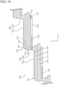
- Fig. 10 is a schematic side view of the photoelectric conversion module according to the third embodiment.
- the same reference numerals are given to the same configurations as those of the first embodiment and the second embodiment. It should be noted that description of configurations similar to those of the first embodiment and the second embodiment may be omitted.
- the third embodiment is different from the first embodiment in the position of the second connection portion 220 of the connector 200.
- the second connection portion 220 of the connector 200 is provided in a region that does not contribute to photoelectric conversion in the second photoelectric conversion element 10b as viewed in the thickness direction.
- the region of the second photoelectric conversion element 10b that does not contribute to photoelectric conversion may be, for example, a region covered by the collector electrode 30b, a region covered by a photoelectric conversion element (an element on a side opposite to the first photoelectric conversion element 10a) adjacent to the second photoelectric conversion element 10b, and/or a region where the photoelectric conversion layer 26b does not exist at an end portion of the second photoelectric conversion element 10b.
- the connector 200 extends to a position overlapping the second portion 32b of the collector electrode 30b of the second photoelectric conversion element 10b when viewed from the thickness direction in the arrangement direction in which the first photoelectric conversion element 10a and the second photoelectric conversion element 10b are arranged.
- the second connection portion 220 of the connector 200 is provided at a position overlapping the second portion 32b of the collector electrode 30b of the second photoelectric conversion element 10b when viewed from the thickness direction. It should be noted that a position overlapping the second portion 32b of the collector electrode 30b of the second photoelectric conversion element 10b when viewed from the thickness direction corresponds to a region that does not contribute to photoelectric conversion.
- the photoelectric conversion layer 26b When the energy supplied for the connection of the connector 200, for example, the energy supplied by welding is increased, the photoelectric conversion layer 26b may be damaged.
- the region of the photoelectric conversion layer 26b that may be damaged due to the connection in the second connection portion 220 of the connector 200 corresponds to a region that does not contribute to photoelectric conversion in the second photoelectric conversion element 10b. Therefore, it is possible to suppress the possibility that the region contributing to photoelectric conversion in the photoelectric conversion layer 26b is damaged at the time of connecting the connector 200, and it is possible to suppress a decrease in photoelectric conversion efficiency.
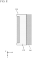
- Fig. 11 is a schematic plan view of a connector included in the photoelectric conversion module according to the fourth embodiment.
- Fig. 11 illustrates a surface of the connector facing the first photoelectric conversion element 10a.
- the connector 200 includes a mesh-like conductive member 240.
- the conductive member 240 constituting the connector 200 has a mesh shape, the area of the conductive member 240 is reduced. Therefore, damage to the photoelectric conversion layers 26a and 26b due to connection at the time of forming the first connection portion 210 and the second connection portion 220 can be suppressed.
- the connector 200 preferably includes the insulator 230 as described above.
- the other configurations and the method for manufacturing the photoelectric conversion module are similar to those of the first embodiment, and thus the description thereof will be omitted.
- Fig. 12 is a schematic plan view of each photoelectric conversion element constituting the photoelectric conversion module according to the fifth embodiment.
- the same reference numerals are given to the same configurations as those of the first to fourth embodiments. It should be noted that description of configurations similar to those of the first to fourth embodiments may be omitted.
- the collector electrodes 30a and 30b of the first photoelectric conversion element 10a and the second photoelectric conversion element 10b have a plurality of substantially linear first portions 31a and 31b and second portions 32a and 32b connected to the plurality of first portions 31a and 31b.
- the second portions 32a and 32b of the collector electrodes 30a and 30b are divided into a plurality of sections (see Fig. 12 ). Specifically, the second portions 32a and 32b of the collector electrodes 30a and 30b are divided into sections corresponding to some of the first portions 31a and 31b.
- the connector 200 is preferably connected to all of the second portions 32a and 32b divided into a plurality of sections. In this case, as compared with the case where the second portions 32a and 32b of the collector electrodes 30a and 30b are continuously connected and extend, thermal damage due to the connection of the connector 200 can be reduced.
- the second portions 32a and 32b of the collector electrodes 30a and 30b are divided into several sections, stress due to heat at the time of connection or at the time of use is also dispersed in each section. Therefore, stress due to heat at the time of connection or use can be alleviated, and breakage, peeling, and the like of the connector 200 can be suppressed.
- the second portions 32a and 32b of the collector electrodes 30a and 30b are not linear but extend in a zigzag shape. As described above, the second portions 32a and 32b of the collector electrodes 30a and 30b may extend in a bent or curved manner.
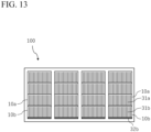
- Fig. 13 is a schematic plan view of a photoelectric conversion module according to a sixth embodiment.
- the same reference numerals are given to the same configurations as those of the first embodiment. It should be noted that the description of the same configuration as that of the first embodiment may be omitted.
- the photoelectric conversion module 100 may include one or a plurality of photoelectric conversion elements 10a and 10b. Note that Fig. 13 illustrates the photoelectric conversion module 100 including the plurality of photoelectric conversion elements 10a and 10b.
- the one or more photoelectric conversion elements 10a and 10b may be sealed with, for example, a sealing material.
- the plurality of photoelectric conversion elements 10a and 10b may be arranged in at least one direction, and preferably may be arranged in a lattice pattern. In this case, the plurality of photoelectric conversion elements 10a and 10b may be electrically connected to each other in series and/or in parallel.
- the second photoelectric conversion element 10b may be disposed so as to cover the second portion 32a of the collector electrode 30a of the first photoelectric conversion element 10a adjacent thereto.
- the second photoelectric conversion element 10b is electrically connected to the second portion 32a of the collector electrode 30a of the first photoelectric conversion element 10a adjacent thereto.
- the photoelectric conversion elements 10a and 10b adjacent to each other may be electrically connected to each other by the connector 200 described above.
- the connector 200 may extend across the photoelectric conversion elements 10a and 10b adjacent to each other.
- the photoelectric conversion elements 10a and 10b adjacent to each other may be arranged at intervals.
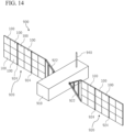
- FIG. 14 is a schematic perspective view of an artificial satellite including a photoelectric conversion module.
- An artificial satellite 900 may have a base portion 910 and a paddle 920.
- the base portion 910 may include a device (not illustrated) necessary for controlling the artificial satellite 900 and the like.
- An antenna 940 may be attached to the base portion 910.
- the paddle 920 may include the photoelectric conversion module 100 described above.
- the paddle 920 including the photoelectric conversion module 100 can be used as a power source for operating various devices provided in the base portion 910.
- the photoelectric conversion module 100 can be applied to a paddle for an artificial satellite.
- the photoelectric conversion module 100 including the photoelectric conversion element 10a, 10b having high heat resistance described above since the paddle 920 for an artificial satellite is exposed to a high temperature environment and a severe temperature change environment at the time of launching and operating the artificial satellite, it is desirable to use the photoelectric conversion module 100 including the photoelectric conversion element 10a, 10b having high heat resistance described above.
- the paddle 920 may include a connecting portion 922 and a hinge portion 924.
- the connecting portion 922 corresponds to a portion connecting the paddle 920 to the base portion 910.
- the hinge portion 924 extends along one direction, and the paddle 920 can be bent with the hinge portion 924 as a rotation axis.
- Each paddle 920 may have at least one, preferably a plurality of, hinge portions 924.
- the paddle 920 including the photoelectric conversion module 100 is configured to be small and foldable.
- the paddle 920 may be in a folded state.
- the paddle 920 may be deployed when receiving sunlight to generate power.
- the paddle 920 may have a cylindrical shape formed by being wound. Accordingly, the paddle 920 can take a substantially flat developed state by the rotation of the wound portion. When the artificial satellite 900 is launched, the paddle 920 may maintain a generally cylindrical shape. The paddle 920 may be unfolded in a substantially flat state when receiving sunlight to generate power.
- each feature described in each of the foregoing embodiments may be applied to or replaced with another embodiment as much as possible.
- the thin-film photoelectric conversion element has been described as an example, but the present invention is not limited thereto, and can be applied to a crystalline photoelectric conversion element as much as possible.
- the connector 200 is connected to the second portion 32a of the collector electrode 30a of the first photoelectric conversion element 10a at the first connection portion 210.
- the connector 200 may be directly connected to the second electrode layer 24a of the first photoelectric conversion element 10a at the first connection portion 210, or may be connected to a connection pad provided on the second electrode layer 24a.
- one connector 200 connects the first photoelectric conversion element 10a and the second photoelectric conversion element 10b.
- the first photoelectric conversion element 10a and the second photoelectric conversion element 10b may be connected to each other by a plurality of connectors 200.
- the connector 200 may be constituted by elongated members arranged in parallel with each other.
- a so-called CIS-based thin-film photoelectric conversion element has been described as an example of the photoelectric conversion elements 10a and 10b. It should be noted that the present invention is not limited thereto, and can also be applied to a crystalline photoelectric conversion element containing silicon.
Landscapes
- Engineering & Computer Science (AREA)
- Life Sciences & Earth Sciences (AREA)
- Sustainable Development (AREA)
- Remote Sensing (AREA)
- Aviation & Aerospace Engineering (AREA)
- Photovoltaic Devices (AREA)
- Manufacturing & Machinery (AREA)
Abstract
Description
- The present invention relates to a photoelectric conversion module, a paddle, and a method for manufacturing a photoelectric conversion module.
- Photoelectric conversion modules that convert light energy into electrical energy are known (Patent Literature 1). The photoelectric conversion module described in Patent Literature 1 includes a plurality of photoelectric conversion elements. End portions of the photoelectric conversion elements adjacent to each other are overlapped with each other. The photoelectric conversion elements adjacent to each other are electrically connected to each other by a conductor such as solder in a region overlapping each other (see
Fig. 5 of Patent Literature 1). - Patent Literature 1:
JP 2016-119401 A - An overlapping region (non-power generation region) between photoelectric conversion elements adjacent to each other is preferably as narrow as possible. However, when the overlapping region is narrow, the area of a conductor such as solder connecting the photoelectric conversion elements is reduced, and thus connection strength may be reduced. For example, in a photoelectric conversion module for a mobile object such as space, air or a vehicle, a load such as vibration applied to the mobile object may apply a large load to a connection portion between the photoelectric conversion elements.
- Therefore, a photoelectric conversion module capable of connecting photoelectric conversion elements with stable connection strength and a method for manufacturing the photoelectric conversion module are desired.
- A photoelectric conversion module according to one aspect comprises: a first photoelectric conversion element; a second photoelectric conversion element; and a connector. The first photoelectric conversion element and the second photoelectric conversion element are arranged side by side so as to partially overlap each other. The connector is connected to the first photoelectric conversion element at a first connection portion. The connector is connected to the second photoelectric conversion element at a second connection portion away from the first connection portion.
- A method for manufacturing a photoelectric conversion module comprises: a step of preparing a first photoelectric conversion element, a second photoelectric conversion element, and a connector; a step of connecting the connector to the first photoelectric conversion element at a first connection portion; a step of arranging the first photoelectric conversion element and the second photoelectric conversion element side by side so as to partially overlap each other; and a step of connecting the connector to the second photoelectric conversion element at a second connection portion away from the first connection portion.
- A paddle according to one aspect comprises said photoelectric conversion module.
-
-
Fig. 1 is a schematic plan view of a photoelectric conversion module according to a first embodiment. -
Fig. 2 is a schematic side view of the photoelectric conversion module according to the first embodiment as viewed from a Y direction inFig. 1 . -
Fig. 3 is a schematic plan view of each photoelectric conversion element constituting the photoelectric conversion module. -
Fig. 4 is a schematic plan view of a connector connecting photoelectric conversion modules adjacent to each other. -
Fig. 5 is a schematic view for explaining a region of an insulator of the connector. -
Fig. 6 is a schematic view for explaining one step in a method for manufacturing the photoelectric conversion module. -
Fig. 7 is a schematic view for explaining a step following the step illustrated inFig. 6 . -
Fig. 8 is a schematic plan view of a connector for connecting adjacent photoelectric conversion modules according to a second embodiment. -
Fig. 9 is a schematic view for explaining a region of an insulator of the connector according to a second embodiment. -
Fig. 10 is a schematic side view of a photoelectric conversion module according to a third embodiment. -
Fig. 11 is a schematic plan view of a connector included in a photoelectric conversion module according to a fourth embodiment. -
Fig. 12 is a schematic plan view of each photoelectric conversion element constituting a photoelectric conversion module according to a fifth embodiment. -
Fig. 13 is a schematic plan view of a photoelectric conversion module according to a sixth embodiment. -
Fig. 14 is a schematic perspective view of an artificial satellite including a photoelectric conversion module. - Hereinafter, embodiments will be described with reference to the drawings. In the following drawings, the same or similar parts are denoted by the same or similar reference numerals. However, it should be noted that the drawings are schematic, and ratios of dimensions and the like may be different from actual ones.
-
Fig. 1 is a schematic plan view of a photoelectric conversion module according to a first embodiment.Fig. 2 is a schematic side view of the photoelectric conversion module according to the first embodiment as viewed from a Y direction inFig. 1 .Fig. 3 is a schematic plan view of each photoelectric conversion element constituting the photoelectric conversion module.Fig. 4 is a schematic plan view of a connector connecting photoelectric conversion modules adjacent to each other.Fig. 4 illustrates one surface of the connector facing a firstphotoelectric conversion element 10a described later.Fig. 5 is a schematic view for explaining a region of an insulator of the connector. Note that, inFig. 3 , in order to describe the structure of each photoelectric conversion element constituting the photoelectric conversion module, reference numerals related to each photoelectric conversion element are attached. - A
photoelectric conversion module 100 according to the first embodiment includes a plurality ofphotoelectric conversion elements connector 200 that electrically connects thephotoelectric conversion elements photoelectric conversion elements photoelectric conversion elements photoelectric conversion elements photoelectric conversion elements photoelectric conversion elements connector 200 in the overlapping portion. The number ofphotoelectric conversion elements - The
photoelectric conversion elements photoelectric conversion elements - Each of the
photoelectric conversion elements conductive substrates first electrode layers conductive substrates conductive substrates conductive substrates photoelectric conversion elements - When a metal substrate is adopted as the
conductive substrates conductive substrates conductive substrates conductive substrates - When the
conductive substrates photoelectric conversion elements conductive substrates photoelectric conversion module 100 as compared with a glass substrate. - The
photoelectric conversion elements first electrode layers second electrode layers photoelectric conversion layers first electrode layers second electrode layers - The
first electrode layers - The
first electrode layers conductive substrates conductive substrates first electrode layers first electrode layers conductive substrates - In the present embodiment, the second electrode layers 24a and 24b may be constituted by transparent electrode layers. When the second electrode layers 24a and 24b are formed by transparent electrode layers, light incident on the photoelectric conversion layers 26a and 26b or is emitted from the photoelectric conversion layers 26a and 26b passes through the second electrode layers 24a and 24b.
- When the second electrode layers 24a and 24b are formed by transparent electrode layers, the
first electrode layers first electrode layers first electrode layers - As a preferred example, the second electrode layers 24a and 24b may be formed by an n-type semiconductor, more specifically, a material having n-type conductivity and relatively low resistance. The second electrode layers 24a and 24b can also function as an n-type semiconductor and a transparent electrode layer. The second electrode layers 24a and 24b include, for example, a metal oxide to which a group III element (B, Al, Ga, or In) is added as a dopant. Examples of the metal oxide include ZnO and SnO2. The second electrode layer 24 can be selected from, for example, indium tin oxide (In2O3:Sn), indium titanium oxide (In2O3:Ti), indium zinc oxide (In2O3:Zn), tin zinc-doped indium oxide (In2O3:Sn, Zn), tungsten-doped indium oxide (In2O3:W), hydrogen-doped indium oxide (In2O3:H), indium gallium zinc oxide (InGaZnO4), zinc tin oxide (ZnO:Sn), fluorine-doped tin oxide (SnO2:F), gallium-doped zinc oxide (ZnO:Ga), boron-doped zinc oxide (ZnO:B), aluminum-doped zinc oxide (ZnO:Al), and the like.
- Although not particularly limited, the thickness of the second electrode layers 24a and 24b is, for example, 0.5 um to 2.5 µm.
- The photoelectric conversion layers 26a and 26b may include, for example, a p-type semiconductor. In a specific example, the photoelectric conversion layers 26a and 26b may function as, for example, a polycrystalline or microcrystalline p-type compound semiconductor layer. Although not particularly limited, the thickness of the photoelectric conversion layers 26a and 26b is, for example, 1.0 um to 3.0 um.
- In a specific example, the photoelectric conversion layers 26a and 26b are formed by a chalcogen semiconductor containing a chalcogen element, and function as a polycrystalline or microcrystalline p-type compound semiconductor layer. The photoelectric conversion layers 26a and 26b may be made of, for example, a group I-III-VI2 compound semiconductor having a chalcopyrite structure containing a group I element, a group III element and a group VI element (chalcogen element). Here, the group I element can be selected from copper (Cu), silver (Ag) gold (Au) and the like. The group III element can be selected from indium (In), gallium (Ga), aluminum (Al) and the like. In addition, the photoelectric conversion layers 26a and 26b may contain tellurium (Te) or the like in addition to selenium (Se) and sulfur (S) as the group VI element. In addition, the photoelectric conversion layers 26a and 26b may contain alkali metals such as Li, Na, K, Rb and Cs.
- Alternatively, the photoelectric conversion layers 26a and 26b may be made of a group I2-(II-IV)-VI4 compound semiconductor which is a CZTS-based chalcogen semiconductor containing Cu, Zn, Sn, S or Se. Representative examples of the CZTS-based chalcogen semiconductor include those using a compound such as Cu2ZnSnSe4 or Cu2ZnSn(S,Se)4.
- The photoelectric conversion layers 26a and 26b are not limited to those described above, and may be made of any material that causes photoelectric conversion.
- The
photoelectric conversion elements first electrode layers first electrode layers first electrode layers - The first buffer layer is not particularly limited, but may be, for example, a layer containing a chalcogenide compound of a transition metal element having a layered structure. Specifically, the first buffer layer may be made of a compound including a transition metal material such as Mo, W, Ti, V, Cr, Nb or Ta and a chalcogen element such as O, S or Se. The first buffer layer may be, for example, Mo(Se,S)2 layer, a MoSe2 layer, MoS2 layer, or the like.
- The
photoelectric conversion elements - The second buffer layer can be selected from compounds containing zinc (Zn), cadmium (Cd) and indium (In). Examples of the compound containing zinc include ZnO, ZnS, Zn(OH)2, or Zn(O,S) and Zn(O,S,OH) which are mixed crystals thereof, and further include ZnMgO and ZnSnO. Examples of the compound containing cadmium include CdS, CdO, or Cd(O,S) and Cd(O,S,OH) which are mixed crystals of CdS and CdO. Examples of the compound containing indium include In2S3 and In2O3, or In2(O,S)3 and In2(O,S,OH)3 which are mixed crystals of In2S3 and In2O3, and In2O3, In2S3, In(OH)x, and the like can be used. The second buffer layer may have a laminated structure of these compounds.
- The second buffer layer has an effect of improving characteristics such as photoelectric conversion efficiency, but this can be omitted. When the second buffer layer is omitted, the second electrode layers 24a and 24b are formed directly on the photoelectric conversion layers 26a and 26b.
- It should be noted that the laminated structure of the
photoelectric conversion elements photoelectric conversion elements photoelectric conversion elements - The
photoelectric conversion elements collector electrodes collector electrodes collector electrodes collector electrodes - The
collector electrodes first portions second portions first portions first portions second portions - The
first portions first portions second portions - In the illustrated aspect, the substantially linear
first portions first portions - The plurality of the
first portions collector electrodes first portions second portions first portions second portions - The
second portions collector electrodes second portions first portions first portions first portions second portions - The
second portions collector electrodes photoelectric conversion elements second portions collector electrodes first portions - The
collector electrodes first portions second portions collector electrodes first portions second portions collector electrodes collector electrodes - The
second portions collector electrodes photoelectric conversion elements Fig. 3 ). Thesecond portions collector electrodes photoelectric conversion elements - The
connector 200 mechanically and electrically connects thephotoelectric conversion elements connector 200 may include aconductive member 240. Theconnector 200 may be, for example, a ribbon wire of a conductive metal including Ag, Ni, Co, Fe, Cr, Mo, Mn, Cu, Al, Ti, or a combination thereof. Furthermore, theconnector 200 may be made of an alloy containing some of the above-described conductive metals, such as an alloy Kovar or stainless steel (SUS). - Next, a structure related to connection between the
photoelectric conversion elements photoelectric conversion elements photoelectric conversion elements photoelectric conversion element 10a on the left side in the drawing is referred to as the "first photoelectric conversion element", and thephotoelectric conversion element 10b on the right side in the drawing is referred to as the "second photoelectric conversion element". However, it should be noted that the terms the "first photoelectric conversion element" and the "second photoelectric conversion element" are merely used for convenience to distinguish the elements. Each of the first photoelectric conversion element and the second photoelectric conversion element may have the structure of thephotoelectric conversion elements - The
connector 200 is connected to the firstphotoelectric conversion element 10a at afirst connection portion 210. Theconnector 200 may be connected to, for example, thecollector electrode 30a of the firstphotoelectric conversion element 10a or a connection pad (not illustrated) provided in thecollector electrode 30a of the firstphotoelectric conversion element 10a at thefirst connection portion 210. In the aspect illustrated inFig. 2 , theconnector 200 is directly connected to thesecond portion 32a of thecollector electrode 30a of the firstphotoelectric conversion element 10a at thefirst connection portion 210. Alternatively, theconnector 200 may be connected to thesecond portion 32a of thecollector electrode 30a of the firstphotoelectric conversion element 10a via a connection pad (not illustrated) at thefirst connection portion 210. - The
connector 200 is connected to the secondphotoelectric conversion element 10b at asecond connection portion 220 away from thefirst connection portion 210. For example, theconnector 200 may be connected to theconductive substrate 20b of the secondphotoelectric conversion element 10b or theconnection pad 50 provided on theconductive substrate 20b of the secondphotoelectric conversion element 10b. In the aspect illustrated inFig. 2 , theconnector 200 is connected to theconnection pad 50 provided on theconductive substrate 20b of the secondphotoelectric conversion element 10b at thesecond connection portion 220. Alternatively, theconnector 200 may be directly connected to theconductive substrate 20b of the secondphotoelectric conversion element 10b at thesecond connection portion 220. Theconnection pad 50 may be, for example, a metal film such as aluminum. In this case, the material constituting theconnection pad 50 and the material constituting theconnector 200 are mutually diffused with heat generated at the time of connection, whereby theconnector 200 can be more firmly connected. - The length of the
connector 200 in an arrangement direction (X direction in the drawing) in which the firstphotoelectric conversion element 10a and the secondphotoelectric conversion element 10b are arranged may be smaller than the length of the secondphotoelectric conversion element 10b in the arrangement direction. As a result, theconnector 200 is provided in a region covered with the secondphotoelectric conversion element 10b as viewed in the thickness direction. For example, theconnector 200 may extend from the region of thesecond portion 32a of thecollector electrode 30a of the firstphotoelectric conversion element 10a toward the side opposite to thefirst portion 31a with respect to thesecond portion 32a. - With the above-described configuration, the
connector 200 electrically connects the electrodes (conductive members) having different polarities of the firstphotoelectric conversion element 10a and the secondphotoelectric conversion element 10b to each other. Theconnector 200 may be connected by , for example, soldering or welding at thefirst connection portion 210 and thesecond connection portion 220. Preferably, theconnector 200 is connected by welding such as, but not limited to, parallel gap resistance welding at thefirst connection portion 210 and thesecond connection portion 220. Theconnector 200 is firmly connected to the firstphotoelectric conversion element 10a and the secondphotoelectric conversion element 10b at different positions, that is, at thefirst connection portion 210 and thesecond connection portion 220. Therefore, it is possible to provide thephotoelectric conversion module 100 capable of connecting thephotoelectric conversion elements - The
conductive substrate 20b of the secondphotoelectric conversion element 10b is disposed so as to overlap a part of thecollector electrode 30a of the firstphotoelectric conversion element 10a (seeFigs. 1 and2 ). Specifically, theconductive substrate 20b of the secondphotoelectric conversion element 10b may cover at least a part of thesecond portion 32a of thecollector electrode 30a of the firstphotoelectric conversion element 10a as viewed in the thickness direction (Z direction in the drawing). - The second
photoelectric conversion element 10b preferably does not cover thefirst portion 31a of thecollector electrode 30a of the firstphotoelectric conversion element 10a. As a result, the region of the firstphotoelectric conversion element 10a exposed from the secondphotoelectric conversion element 10b increases, so that a wide region where photoelectric conversion can be performed by the firstphotoelectric conversion element 10a can be secured. Therefore, the photoelectric conversion efficiency of the entirephotoelectric conversion module 100 can be improved. - The second
photoelectric conversion element 10b covers at least a part, preferably the entiresecond portion 32a of thecollector electrode 30a of the firstphotoelectric conversion element 10a. More preferably, the secondphotoelectric conversion element 10b is disposed so as to substantially not cover thefirst portion 31a while substantially entirely covering thesecond portion 32a of thecollector electrode 30a of the firstphotoelectric conversion element 10a. As a result, the firstphotoelectric conversion element 10a and the secondphotoelectric conversion element 10b can be densely arranged such that a region that does not contribute to photoelectric conversion, that is, a region of thesecond portion 32a is not exposed. Therefore, the size of the photoelectric conversion module as a whole can be reduced without reducing the efficiency of photoelectric conversion. - The
first connection portion 210 of theconnector 200 may be provided in a region sandwiched between the firstphotoelectric conversion element 10a and the secondphotoelectric conversion element 10b. In other words, thefirst connection portion 210 of theconnector 200 is provided in a region where the firstphotoelectric conversion element 10a and the secondphotoelectric conversion element 10b overlap each other as viewed in the thickness direction (Z direction in the drawing). As a result, thefirst connection portion 210 is provided in a region that does not contribute to photoelectric conversion. Even in this case, theconnector 200 may not be connected to the secondphotoelectric conversion element 10b at thefirst connection portion 210. - The
second connection portion 220 of theconnector 200 may be provided in a region overlapping the secondphotoelectric conversion element 10b as viewed in the thickness direction. As a result, thesecond connection portion 220 is provided in a region that does not contribute to photoelectric conversion. Furthermore, thesecond connection portion 220 of theconnector 200 is preferably provided at a position not overlapping the firstphotoelectric conversion element 10a as viewed in the thickness direction. As a result, as will be described later, theconnector 200 can be easily connected by thesecond connection portion 220 at the time of manufacturing thephotoelectric conversion module 100. - The
connector 200 may have aninsulator 230 between thefirst connection portion 210 and the second connection portion 220 (seeFig. 4 ). Theinsulator 230 may be provided on a surface of theconnector 200 facing the firstphotoelectric conversion element 10a. It should be noted that theinsulator 230 is provided so as not to hinder conductivity between thefirst connection portion 210 and thesecond connection portion 220 of theconnector 200. - The
insulator 230 may be constituted by, for example, an insulating layer provided on theconductive member 240 constituting theconnector 200. In this case, theinsulator 230 can be configured, for example, by forming and/or applying an insulating layer on a conductive member constituting theconnector 200. - Instead of the above-described aspect, the
insulator 230 may be made of, for example, an oxide formed by oxidation of theconductive member 240 constituting theconnector 200. Such aninsulator 230 can be formed by, for example, oxidizing Al, Ti, Kovar, or the like forming theconnector 200. Examples of the oxidation treatment include anodization and oxidation by annealing. As described above, when theinsulator 230 is formed by oxidation of theconductive member 240 constituting theconnector 200, theinsulator 230 may be formed on both surfaces of theconnector 200, that is, on both the surface facing the firstphotoelectric conversion element 10a and the surface facing the secondphotoelectric conversion element 10b. - The
insulator 230 may cover at least one end portion of thefirst electrode layer 22a of the firstphotoelectric conversion element 10a and thephotoelectric conversion layer 26a of the firstphotoelectric conversion element 10a, the end portion being located in the region between thefirst connection portion 210 and thesecond connection portion 220 when viewed from the thickness direction. Furthermore, theinsulator 230 may cover an end portion of theconductive substrate 20a of the firstphotoelectric conversion element 10a, the end portion being located in a region between thefirst connection portion 210 and thesecond connection portion 220 when viewed from the thickness direction. - The end portion of the
conductive substrate 20a covered with theinsulator 230 may be a region of theconductive substrate 20a exposed from thefirst electrode layer 22a, thephotoelectric conversion layer 26a, or thesecond electrode layer 24a. The end portion of thefirst electrode layer 22a covered with theinsulator 230 may be a region of thefirst electrode layer 22a exposed from thephotoelectric conversion layer 26a or thesecond electrode layer 24a. The end portion of thephotoelectric conversion layer 26a covered with theinsulator 230 may be a region of thephotoelectric conversion layer 26a exposed from thesecond electrode layer 24a. -
Fig. 5 is a schematic view for explaining a region of an insulator of the connector. A region R1 illustrated inFig. 5 indicates a region covered with theinsulator 230. As illustrated inFig. 5 , in the first embodiment, theinsulator 230 of theconnector 200 covers a region opposite to thefirst portion 31a with respect to thesecond portion 32a of thecollector electrode 30a of the firstphotoelectric conversion element 10a. - Preferably, the
insulator 230 of theconnector 200 may extend from one end to the other end of theconnector 200 in the Y direction of the drawing along the extending direction of thesecond portion 32a of thecollector electrode 30a of the firstphotoelectric conversion element 10a. - In the first embodiment, the sizes (areas) of the
conductive substrates first electrode layers conductive substrates first electrode layers insulator 230 of theconnector 200 may cover, for example, portions of theconductive substrate 20a and thefirst electrode layer 22a extending from thephotoelectric conversion layer 26a and thesecond electrode layer 24a. Thus, theconductive substrate 20b of the secondphotoelectric conversion element 10b can be prevented from electrically contacting thefirst electrode layer 22a and/or theconductive substrate 20a of the firstphotoelectric conversion element 10a. Similarly, when theinsulator 230 covers the region of thephotoelectric conversion layer 26a exposed from thesecond electrode layer 24a, theconductive substrate 20b of the secondphotoelectric conversion element 10b can be prevented from electrically contacting thephotoelectric conversion layer 26a of the firstphotoelectric conversion element 10a. Therefore, an electrical short circuit between the firstphotoelectric conversion element 10a and the secondphotoelectric conversion element 10b can be suppressed. - Instead of the illustrated aspect, the sizes (areas) of the
conductive substrate 20a and thefirst electrode layer 22a may be substantially the same as the sizes (areas) of thephotoelectric conversion layer 26a and thesecond electrode layer 24a. Even in this case, the outer edges of theconductive substrate 20a, thefirst electrode layer 22a, and thephotoelectric conversion layer 26a are exposed on the side surface of the firstphotoelectric conversion element 10a. In this case, theinsulator 230 of theconnector 200 may cover the outer edge portions of theconductive substrate 20a, thefirst electrode layer 22a, and thephotoelectric conversion layer 26a when viewed from the thickness direction. Even in this case, theconductive substrate 20b of the secondphotoelectric conversion element 10b can be prevented from electrically contacting thefirst electrode layer 22a, theconductive substrate 20a, and/or thephotoelectric conversion layer 26a of the firstphotoelectric conversion element 10a. - The configurations of the connection portions of the two
photoelectric conversion elements - The
photoelectric conversion module 100 including the plurality ofphotoelectric conversion elements photoelectric conversion elements conductive substrates photoelectric conversion elements photoelectric conversion module 100 may have a support substrate (not illustrated) that supports the entire plurality ofphotoelectric conversion elements - Next, a method for manufacturing the
photoelectric conversion module 100 according to the first embodiment will be described with reference toFigs. 6 and7 .Fig. 6 is a schematic view for explaining one step in the method for manufacturing the photoelectric conversion module.Fig. 7 is a schematic view for describing a step subsequent to the step illustrated inFig. 6 . - First, the first
photoelectric conversion element 10a and the secondphotoelectric conversion element 10b each including thefirst electrode layers first electrode layers connector 200 are prepared. The firstphotoelectric conversion element 10a, the secondphotoelectric conversion element 10b, and theconnector 200 may have the above-described structure. - In the manufacturing process of each of the
photoelectric conversion elements first electrode layers conductive substrates conductive substrates - The
first electrode layers first electrode layers conductive substrates first electrode layers first electrode layers - The photoelectric conversion layers 26a and 26b are formed on the
first electrode layers first electrode layers - The second buffer layer is formed on the
photoelectric conversion layer - The second electrode layers 24a and 24b are formed on the second buffer layer by a method such as a sputtering method, a CVD method or an ALD method. Alternatively, when the second buffer layer is not present, the second electrode layers 24a and 24b are formed on the photoelectric conversion layers 26a and 26b. The materials constituting the second electrode layers 24a and 24b are as described above.
- Next,
collector electrodes first portions second portions collector electrodes - Next, the
connector 200 is connected to the second conductive member on the second electrode side of the firstphotoelectric conversion element 10a at thefirst connection portion 210. In the first embodiment, theconnector 200 is connected to thesecond portion 32a of thecollector electrode 30a of the firstphotoelectric conversion element 10a at the first connection portion 210 (see the arrow P1 inFig. 6 ). - The
connector 200 may be welded to thesecond portion 32a of thecollector electrode 30a of the firstphotoelectric conversion element 10a by, for example, a parallel gap welding method using a resistance welding machine with a transistor control method. - Next, the first
photoelectric conversion element 10a and the secondphotoelectric conversion element 10b are arranged side by side so as to partially overlap each other (seeFig. 7 ). At this time, thefirst connection portion 210 of theconnector 200 may be covered with the secondphotoelectric conversion element 10b. In this case, theconnector 200 may not be connected to the secondphotoelectric conversion element 10b at thefirst connection portion 210. Thesecond connection portion 220, which will be described later, of theconnector 200 is located in a region not overlapping the firstphotoelectric conversion element 10a as viewed in the thickness direction. - Next, the
connector 200 is connected to the first conductive member on the first electrode side of the secondphotoelectric conversion element 10b at thesecond connection portion 220 away from thefirst connection portion 210. In the first embodiment, theconnector 200 is connected to theconnection pad 50 provided on theconductive substrate 20b of the secondphotoelectric conversion element 10b at the second connection portion 220 (see the arrow P2 inFig. 7 ). Note that, as described above, theconnection pad 50 may not be provided. In this case, theconnector 200 may be directly connected to theconductive substrate 20b of the secondphotoelectric conversion element 10b at thesecond connection portion 220. - Here, the
second connection portion 220, which will be described later, of theconnector 200 is located in a region that does not overlap with the firstphotoelectric conversion element 10a when viewed from the thickness direction. Therefore, theconnector 200 can be easily connected to theconductive substrate 20b of the secondphotoelectric conversion element 10b without being hindered by the firstphotoelectric conversion element 10a. - By repeating the above connection step, a large number of photoelectric conversion elements can be coupled side by side with each other.
- Next, a photoelectric conversion module according to a second embodiment will be described with reference to
Figs. 8 and9 .Fig. 8 is a schematic plan view of a connector that connects adjacent photoelectric conversion modules according to the second embodiment.Fig. 8 illustrates one surface of theconnector 200 facing the firstphotoelectric conversion element 10a.Fig. 9 is a schematic view for explaining a region of an insulator of the connector according to the second embodiment. The same components as those of the first embodiment are denoted by the same reference numerals. It should be noted that the description of the same configuration as that of the first embodiment may be omitted. - The second embodiment is different from the first embodiment in a region where the
insulator 230 of theconnector 200 is provided. In the second embodiment, theinsulator 230 has a substantially U-shape defined by a region covered with the secondphotoelectric conversion element 10b in the end portion of the firstphotoelectric conversion element 10a. - Specifically, the
insulator 230 covers the entire region covered by the secondphotoelectric conversion element 10b at the end portions of theconductive substrate 20a, thefirst electrode layer 22a, and thephotoelectric conversion layer 26a of the firstphotoelectric conversion element 10a. Therefore, as illustrated inFig. 9 , theinsulator 230 covers a substantially U-shaped region along the periphery of thesecond portion 32a of thecollector electrode 30a of the firstphotoelectric conversion element 10a in plan view. - This makes it possible to more reliably prevent the
conductive substrate 20a, thefirst electrode layer 22a, and/or thephotoelectric conversion layer 26a of the first photoelectric conversion element 10 from coming into contact with theconductive substrate 20b of the secondphotoelectric conversion element 10b. - The other configurations and the method for manufacturing the photoelectric conversion module are similar to those of the first embodiment, and thus the description thereof will be omitted.
- Next, a photoelectric conversion module according to a third embodiment will be described with reference to
Fig. 10. Fig. 10 is a schematic side view of the photoelectric conversion module according to the third embodiment. The same reference numerals are given to the same configurations as those of the first embodiment and the second embodiment. It should be noted that description of configurations similar to those of the first embodiment and the second embodiment may be omitted. - The third embodiment is different from the first embodiment in the position of the
second connection portion 220 of theconnector 200. In the third embodiment, thesecond connection portion 220 of theconnector 200 is provided in a region that does not contribute to photoelectric conversion in the secondphotoelectric conversion element 10b as viewed in the thickness direction. Here, the region of the secondphotoelectric conversion element 10b that does not contribute to photoelectric conversion may be, for example, a region covered by thecollector electrode 30b, a region covered by a photoelectric conversion element (an element on a side opposite to the firstphotoelectric conversion element 10a) adjacent to the secondphotoelectric conversion element 10b, and/or a region where thephotoelectric conversion layer 26b does not exist at an end portion of the secondphotoelectric conversion element 10b. - In a specific example, the
connector 200 extends to a position overlapping thesecond portion 32b of thecollector electrode 30b of the secondphotoelectric conversion element 10b when viewed from the thickness direction in the arrangement direction in which the firstphotoelectric conversion element 10a and the secondphotoelectric conversion element 10b are arranged. Thesecond connection portion 220 of theconnector 200 is provided at a position overlapping thesecond portion 32b of thecollector electrode 30b of the secondphotoelectric conversion element 10b when viewed from the thickness direction. It should be noted that a position overlapping thesecond portion 32b of thecollector electrode 30b of the secondphotoelectric conversion element 10b when viewed from the thickness direction corresponds to a region that does not contribute to photoelectric conversion. - When the energy supplied for the connection of the
connector 200, for example, the energy supplied by welding is increased, thephotoelectric conversion layer 26b may be damaged. According to the above configuration, the region of thephotoelectric conversion layer 26b that may be damaged due to the connection in thesecond connection portion 220 of theconnector 200 corresponds to a region that does not contribute to photoelectric conversion in the secondphotoelectric conversion element 10b. Therefore, it is possible to suppress the possibility that the region contributing to photoelectric conversion in thephotoelectric conversion layer 26b is damaged at the time of connecting theconnector 200, and it is possible to suppress a decrease in photoelectric conversion efficiency. - The other configurations and the method for manufacturing the photoelectric conversion module are similar to those of the first embodiment, and thus the description thereof will be omitted.
- Next, a photoelectric conversion module according to a fourth embodiment will be described with reference to
Fig. 11. Fig. 11 is a schematic plan view of a connector included in the photoelectric conversion module according to the fourth embodiment.Fig. 11 illustrates a surface of the connector facing the firstphotoelectric conversion element 10a. - In the fourth embodiment, the
connector 200 includes a mesh-likeconductive member 240. When theconductive member 240 constituting theconnector 200 has a mesh shape, the area of theconductive member 240 is reduced. Therefore, damage to the photoelectric conversion layers 26a and 26b due to connection at the time of forming thefirst connection portion 210 and thesecond connection portion 220 can be suppressed. - Also in the fourth embodiment, the
connector 200 preferably includes theinsulator 230 as described above. The other configurations and the method for manufacturing the photoelectric conversion module are similar to those of the first embodiment, and thus the description thereof will be omitted. - Next, a photoelectric conversion module according to a fifth embodiment will be described with reference to
Fig. 12. Fig. 12 is a schematic plan view of each photoelectric conversion element constituting the photoelectric conversion module according to the fifth embodiment. The same reference numerals are given to the same configurations as those of the first to fourth embodiments. It should be noted that description of configurations similar to those of the first to fourth embodiments may be omitted. - In the fifth embodiment, the
collector electrodes photoelectric conversion element 10a and the secondphotoelectric conversion element 10b have a plurality of substantially linearfirst portions second portions first portions - In the fifth embodiment, the
second portions collector electrodes Fig. 12 ). Specifically, thesecond portions collector electrodes first portions connector 200 is preferably connected to all of thesecond portions second portions collector electrodes connector 200 can be reduced. Here, since thesecond portions collector electrodes connector 200 can be suppressed. - In the fifth embodiment, the
second portions collector electrodes second portions collector electrodes - Next, a photoelectric conversion module according to a sixth embodiment will be described with reference to
Fig. 13. Fig. 13 is a schematic plan view of a photoelectric conversion module according to a sixth embodiment. The same reference numerals are given to the same configurations as those of the first embodiment. It should be noted that the description of the same configuration as that of the first embodiment may be omitted. - The
photoelectric conversion module 100 may include one or a plurality ofphotoelectric conversion elements Fig. 13 illustrates thephotoelectric conversion module 100 including the plurality ofphotoelectric conversion elements photoelectric conversion elements - When the
photoelectric conversion module 100 includes the plurality ofphotoelectric conversion elements photoelectric conversion elements photoelectric conversion elements - In the example illustrated in
Fig. 13 , among thephotoelectric conversion elements Fig. 13 , the secondphotoelectric conversion element 10b may be disposed so as to cover thesecond portion 32a of thecollector electrode 30a of the firstphotoelectric conversion element 10a adjacent thereto. In this case, the secondphotoelectric conversion element 10b is electrically connected to thesecond portion 32a of thecollector electrode 30a of the firstphotoelectric conversion element 10a adjacent thereto. - The
photoelectric conversion elements connector 200 described above. In this case, theconnector 200 may extend across thephotoelectric conversion elements - Instead of the aspect illustrated in
Fig. 13 , thephotoelectric conversion elements - Next, an artificial satellite including a photoelectric conversion module and a paddle for an artificial satellite will be described.
Fig. 14 is a schematic perspective view of an artificial satellite including a photoelectric conversion module. Anartificial satellite 900 may have abase portion 910 and apaddle 920. Thebase portion 910 may include a device (not illustrated) necessary for controlling theartificial satellite 900 and the like. Anantenna 940 may be attached to thebase portion 910. - The
paddle 920 may include thephotoelectric conversion module 100 described above. Thepaddle 920 including thephotoelectric conversion module 100 can be used as a power source for operating various devices provided in thebase portion 910. As described above, thephotoelectric conversion module 100 can be applied to a paddle for an artificial satellite. In particular, since thepaddle 920 for an artificial satellite is exposed to a high temperature environment and a severe temperature change environment at the time of launching and operating the artificial satellite, it is desirable to use thephotoelectric conversion module 100 including thephotoelectric conversion element - The
paddle 920 may include a connectingportion 922 and ahinge portion 924. The connectingportion 922 corresponds to a portion connecting thepaddle 920 to thebase portion 910. - The
hinge portion 924 extends along one direction, and thepaddle 920 can be bent with thehinge portion 924 as a rotation axis. Eachpaddle 920 may have at least one, preferably a plurality of, hingeportions 924. Thus, thepaddle 920 including thephotoelectric conversion module 100 is configured to be small and foldable. When theartificial satellite 900 is launched, thepaddle 920 may be in a folded state. Thepaddle 920 may be deployed when receiving sunlight to generate power. - Instead of the structure as illustrated in
Fig. 14 , thepaddle 920 may have a cylindrical shape formed by being wound. Accordingly, thepaddle 920 can take a substantially flat developed state by the rotation of the wound portion. When theartificial satellite 900 is launched, thepaddle 920 may maintain a generally cylindrical shape. Thepaddle 920 may be unfolded in a substantially flat state when receiving sunlight to generate power. - As described above, the contents of the present invention have been disclosed through the embodiments, but it should not be understood that the description and the drawings constituting a part of the disclosure limit the present invention. From this disclosure, various alternative embodiments, examples, and operational techniques will become apparent to those skilled in the art. Therefore, the technical scope of the present invention is defined only by the matters specifying the invention according to the claims appropriate from the above description.
- Each feature described in each of the foregoing embodiments may be applied to or replaced with another embodiment as much as possible. In the above embodiment, the thin-film photoelectric conversion element has been described as an example, but the present invention is not limited thereto, and can be applied to a crystalline photoelectric conversion element as much as possible.
- In the embodiment described above, the
connector 200 is connected to thesecond portion 32a of thecollector electrode 30a of the firstphotoelectric conversion element 10a at thefirst connection portion 210. Alternatively, theconnector 200 may be directly connected to thesecond electrode layer 24a of the firstphotoelectric conversion element 10a at thefirst connection portion 210, or may be connected to a connection pad provided on thesecond electrode layer 24a. - In the embodiment described above, one
connector 200 connects the firstphotoelectric conversion element 10a and the secondphotoelectric conversion element 10b. Alternatively, the firstphotoelectric conversion element 10a and the secondphotoelectric conversion element 10b may be connected to each other by a plurality ofconnectors 200. In this case, theconnector 200 may be constituted by elongated members arranged in parallel with each other. - In the above-described embodiment, a so-called CIS-based thin-film photoelectric conversion element has been described as an example of the
photoelectric conversion elements - This application claims priority based on
Japanese Patent Application No. 2021-177691 filed on October 29, 2021
Claims (13)
- A photoelectric conversion module comprising:a first photoelectric conversion element;a second photoelectric conversion element; anda connector, whereinthe first photoelectric conversion element and the second photoelectric conversion element are arranged side by side so as to partially overlap each other,the connector is connected to the first photoelectric conversion element at a first connection portion, andthe connector is connected to the second photoelectric conversion element at a second connection portion away from the first connection portion.
- The photoelectric conversion module according to claim 1, wherein the first connection portion is provided in a region between the first photoelectric conversion element and the second photoelectric conversion element, and
the second connection portion is provided at a position not overlapping the first photoelectric conversion element as viewed in a thickness direction. - The photoelectric conversion module according to claim 1 or 2, wherein the first photoelectric conversion element includes a collector electrode, and
the connector is connected to the collector electrode or a connection pad provided on the collector electrode. - The photoelectric conversion module according to claim 3, wherein the collector electrode of the first photoelectric conversion element has a plurality of substantially linear first portions and a second portion connected to the plurality of first portions, and
the second portion is divided into a plurality of sections. - The photoelectric conversion module according to any one of claims 1 to 4, wherein the second photoelectric conversion element includes a conductive substrate, and
the connector is connected to the conductive substrate or a connection pad provided on the conductive substrate. - The photoelectric conversion module according to any one of claims 1 to 5, wherein the second connection portion of the connector is provided in a region that does not contribute to photoelectric conversion in the second photoelectric conversion element as viewed in a thickness direction.
- The photoelectric conversion module according to any one of claims 1 to 6, wherein the connector includes an insulator between the first connection portion and the second connection portion.
- The photoelectric conversion module according to claim 7, whereinthe first photoelectric conversion element includes:a first electrode layer;a second electrode layer; anda photoelectric conversion layer between the first electrode layer and the second electrode layer, andthe insulator covers at least one end portion of the first electrode layer of the first photoelectric conversion element and the photoelectric conversion layer of the first photoelectric conversion element, said end portion being located in a region between the first connection portion and the second connection portion when viewed from a thickness direction.
- The photoelectric conversion module according to claim 7 or 8, wherein the first photoelectric conversion element includes a conductive substrate connected to the first electrode layer of the first photoelectric conversion element, and
the insulator covers an end portion of the conductive substrate of the first photoelectric conversion element, the end portion being located in a region between the first connection portion and the second connection portion as viewed in a thickness direction. - The photoelectric conversion module according to any one of claims 7 to 9, wherein the insulator has a U-shape defined by a region covered with the second photoelectric conversion element in an end portion of the first photoelectric conversion element.
- The photoelectric conversion module according to any one of claims 1 to 10, wherein the connector includes a mesh-like conductive member.
- A method for manufacturing a photoelectric conversion module, the method comprising:a step of preparing a first photoelectric conversion element, a second photoelectric conversion element, and a connector;a step of connecting the connector to the first photoelectric conversion element at a first connection portion;a step of arranging the first photoelectric conversion element and the second photoelectric conversion element side by side so as to partially overlap each other; anda step of connecting the connector to the second photoelectric conversion element at a second connection portion away from the first connection portion.
- A paddle comprising the photoelectric conversion module according to any one of claims 1 to 11.
Applications Claiming Priority (2)
| Application Number | Priority Date | Filing Date | Title |
|---|---|---|---|
| JP2021177691 | 2021-10-29 | ||
| PCT/JP2022/039308 WO2023074573A1 (en) | 2021-10-29 | 2022-10-21 | Photoelectric conversion module, paddle, and method for manufacturing photoelectric conversion module |
Publications (2)
| Publication Number | Publication Date |
|---|---|
| EP4425577A1 true EP4425577A1 (en) | 2024-09-04 |
| EP4425577A4 EP4425577A4 (en) | 2025-11-05 |
Family
ID=86159868
Family Applications (1)
| Application Number | Title | Priority Date | Filing Date |
|---|---|---|---|
| EP22886900.4A Pending EP4425577A4 (en) | 2021-10-29 | 2022-10-21 | PHOTOELECTRIC CONVERSION MODULE, PADDLE AND METHOD FOR MANUFACTURING THE PHOTOELECTRIC CONVERSION MODULE |
Country Status (4)
| Country | Link |
|---|---|
| US (1) | US20250011010A1 (en) |
| EP (1) | EP4425577A4 (en) |
| JP (1) | JPWO2023074573A1 (en) |
| WO (1) | WO2023074573A1 (en) |
Family Cites Families (10)
| Publication number | Priority date | Publication date | Assignee | Title |
|---|---|---|---|---|
| DE4030713A1 (en) * | 1990-09-28 | 1992-04-02 | Telefunken Systemtechnik | Photoelectric solar generator - has flexible intermediate connecting plate designed to prevent solar cell fracture due to temp. change stresses |
| JP3323573B2 (en) * | 1992-03-31 | 2002-09-09 | キヤノン株式会社 | Solar cell module and method of manufacturing the same |
| US20140124014A1 (en) * | 2012-11-08 | 2014-05-08 | Cogenra Solar, Inc. | High efficiency configuration for solar cell string |
| JP2016119401A (en) | 2014-12-22 | 2016-06-30 | 日東電工株式会社 | Photoelectric conversion element and photoelectric conversion device including the same |
| CN105932084B (en) * | 2016-05-06 | 2018-04-03 | 协鑫集成科技股份有限公司 | Solar cell module and preparation method thereof |
| CN109494266B (en) * | 2017-09-11 | 2022-04-12 | Lg电子株式会社 | solar panel |
| JPWO2019146366A1 (en) * | 2018-01-25 | 2021-01-07 | 株式会社カネカ | Solar cell module |
| US20200028013A1 (en) * | 2018-07-20 | 2020-01-23 | Beijing Apollo Ding Rong Solor Technology Co., Ltd. | Photovoltaic device interconnect, photovoltaic device including same, and method of forming interconnect |
| WO2020054129A1 (en) * | 2018-09-11 | 2020-03-19 | 株式会社カネカ | Solar cell device and solar cell module |
| JP2021177691A (en) | 2020-05-08 | 2021-11-11 | 住友電気工業株式会社 | Power generation device |
-
2022
- 2022-10-21 US US18/705,510 patent/US20250011010A1/en active Pending
- 2022-10-21 JP JP2023556400A patent/JPWO2023074573A1/ja active Pending
- 2022-10-21 EP EP22886900.4A patent/EP4425577A4/en active Pending
- 2022-10-21 WO PCT/JP2022/039308 patent/WO2023074573A1/en not_active Ceased
Also Published As
| Publication number | Publication date |
|---|---|
| EP4425577A4 (en) | 2025-11-05 |
| WO2023074573A1 (en) | 2023-05-04 |
| US20250011010A1 (en) | 2025-01-09 |
| JPWO2023074573A1 (en) | 2023-05-04 |
Similar Documents
| Publication | Publication Date | Title |
|---|---|---|
| US20100300514A1 (en) | Solar cell and method for manufacturing solar cell | |
| EP2590224B1 (en) | Photoelectric conversion device | |
| EP2487724A2 (en) | Photovoltaic power-generating apparatus and method for manufacturing same | |
| EP2426731A2 (en) | Solar power generation apparatus and manufacturing method thereof | |
| JP2014530498A (en) | THIN FILM SOLAR MODULE INCLUDING SERIAL CONNECTION AND METHOD FOR SERIALLY CONNECTING A plurality of thin film solar cells | |
| WO2012157449A1 (en) | Semiconductor device, solar cell module, solar cell string, and solar cell array | |
| US12532550B2 (en) | Photoelectric conversion module, paddle, and method for manufacturing photoelectric conversion module | |
| US20110011437A1 (en) | Solar cell and method for manufacturing solar cell | |
| EP4354516A1 (en) | Photoelectric conversion element, manufacturing method for photoelectric conversion element, solar battery module, and paddle | |
| US20250011010A1 (en) | Photoelectric conversion module, paddle, and method for manufacturing photoelectric conversion module | |
| EP2450968B1 (en) | Solar photovoltaic device | |
| US12604541B2 (en) | Photoelectric conversion module, paddle, and method for manufacturing photoelectric conversion module | |
| JP7809651B2 (en) | Electrode structure and manufacturing method for solar cell | |
| JP7702971B2 (en) | Electrode structure and manufacturing method for solar cell | |
| EP4365959A1 (en) | Photoelectric conversion element and method for manufacturing photoelectric conversion element | |
| US20260136681A1 (en) | Photoelectric conversion module and manufacturing method for photoelectric conversion module | |
| JP2011103425A (en) | Photoelectric converter | |
| EP4350780A1 (en) | Photoelectric conversion element, solar cell module, and paddle | |
| US20140144479A1 (en) | Photoelectric conversion module | |
| WO2019235461A1 (en) | Solar cell element | |
| EP3300122A1 (en) | Material structure for a solar cell and a solar cell comprising the material structure | |
| WO2024080262A1 (en) | Interconnector, photoelectric conversion module, and paddle | |
| WO2023120614A1 (en) | Photoelectric conversion element, solar cell module, paddle, and photoelectric conversion element manufacturing method | |
| EP4693418A1 (en) | Photoelectric conversion element, photovoltaic module, flying object and method for manufacturing photoelectric conversion element | |
| WO2024080261A1 (en) | Photoelectric conversion module and manufacturing method for photoelectric conversion module |
Legal Events
| Date | Code | Title | Description |
|---|---|---|---|
| STAA | Information on the status of an ep patent application or granted ep patent |
Free format text: STATUS: THE INTERNATIONAL PUBLICATION HAS BEEN MADE |
|
| PUAI | Public reference made under article 153(3) epc to a published international application that has entered the european phase |
Free format text: ORIGINAL CODE: 0009012 |
|
| STAA | Information on the status of an ep patent application or granted ep patent |
Free format text: STATUS: REQUEST FOR EXAMINATION WAS MADE |
|
| 17P | Request for examination filed |
Effective date: 20240416 |
|
| AK | Designated contracting states |
Kind code of ref document: A1 Designated state(s): AL AT BE BG CH CY CZ DE DK EE ES FI FR GB GR HR HU IE IS IT LI LT LU LV MC ME MK MT NL NO PL PT RO RS SE SI SK SM TR |
|
| DAV | Request for validation of the european patent (deleted) | ||
| DAX | Request for extension of the european patent (deleted) | ||
| REG | Reference to a national code |
Ref country code: DE Ref legal event code: R079 Free format text: PREVIOUS MAIN CLASS: H01L0031050000 Ipc: H10F0019900000 |
|
| A4 | Supplementary search report drawn up and despatched |
Effective date: 20251006 |
|
| RIC1 | Information provided on ipc code assigned before grant |
Ipc: H10F 19/90 20250101AFI20250929BHEP Ipc: H10F 19/30 20250101ALI20250929BHEP |