EP4425537A2 - Hybrid multi-die qfp-qfn package - Google Patents
Hybrid multi-die qfp-qfn package Download PDFInfo
- Publication number
- EP4425537A2 EP4425537A2 EP24159904.2A EP24159904A EP4425537A2 EP 4425537 A2 EP4425537 A2 EP 4425537A2 EP 24159904 A EP24159904 A EP 24159904A EP 4425537 A2 EP4425537 A2 EP 4425537A2
- Authority
- EP
- European Patent Office
- Prior art keywords
- qfn
- qfp
- integrated circuit
- die pad
- hybrid
- Prior art date
- Legal status (The legal status is an assumption and is not a legal conclusion. Google has not performed a legal analysis and makes no representation as to the accuracy of the status listed.)
- Pending
Links
Images



Classifications
-
- H—ELECTRICITY
- H10—SEMICONDUCTOR DEVICES; ELECTRIC SOLID-STATE DEVICES NOT OTHERWISE PROVIDED FOR
- H10W—GENERIC PACKAGES, INTERCONNECTIONS, CONNECTORS OR OTHER CONSTRUCTIONAL DETAILS OF DEVICES COVERED BY CLASS H10
- H10W90/00—Package configurations
-
- H—ELECTRICITY
- H10—SEMICONDUCTOR DEVICES; ELECTRIC SOLID-STATE DEVICES NOT OTHERWISE PROVIDED FOR
- H10W—GENERIC PACKAGES, INTERCONNECTIONS, CONNECTORS OR OTHER CONSTRUCTIONAL DETAILS OF DEVICES COVERED BY CLASS H10
- H10W70/00—Package substrates; Interposers; Redistribution layers [RDL]
- H10W70/40—Leadframes
- H10W70/411—Chip-supporting parts, e.g. die pads
-
- H—ELECTRICITY
- H10—SEMICONDUCTOR DEVICES; ELECTRIC SOLID-STATE DEVICES NOT OTHERWISE PROVIDED FOR
- H10W—GENERIC PACKAGES, INTERCONNECTIONS, CONNECTORS OR OTHER CONSTRUCTIONAL DETAILS OF DEVICES COVERED BY CLASS H10
- H10W70/00—Package substrates; Interposers; Redistribution layers [RDL]
- H10W70/01—Manufacture or treatment
- H10W70/04—Manufacture or treatment of leadframes
- H10W70/042—Etching
-
- H—ELECTRICITY
- H10—SEMICONDUCTOR DEVICES; ELECTRIC SOLID-STATE DEVICES NOT OTHERWISE PROVIDED FOR
- H10W—GENERIC PACKAGES, INTERCONNECTIONS, CONNECTORS OR OTHER CONSTRUCTIONAL DETAILS OF DEVICES COVERED BY CLASS H10
- H10W70/00—Package substrates; Interposers; Redistribution layers [RDL]
- H10W70/40—Leadframes
- H10W70/411—Chip-supporting parts, e.g. die pads
- H10W70/415—Leadframe inner leads serving as die pads
-
- H—ELECTRICITY
- H10—SEMICONDUCTOR DEVICES; ELECTRIC SOLID-STATE DEVICES NOT OTHERWISE PROVIDED FOR
- H10W—GENERIC PACKAGES, INTERCONNECTIONS, CONNECTORS OR OTHER CONSTRUCTIONAL DETAILS OF DEVICES COVERED BY CLASS H10
- H10W74/00—Encapsulations, e.g. protective coatings
- H10W74/10—Encapsulations, e.g. protective coatings characterised by their shape or disposition
- H10W74/111—Encapsulations, e.g. protective coatings characterised by their shape or disposition the semiconductor body being completely enclosed
- H10W74/129—Encapsulations, e.g. protective coatings characterised by their shape or disposition the semiconductor body being completely enclosed forming a chip-scale package [CSP]
-
- H—ELECTRICITY
- H10—SEMICONDUCTOR DEVICES; ELECTRIC SOLID-STATE DEVICES NOT OTHERWISE PROVIDED FOR
- H10W—GENERIC PACKAGES, INTERCONNECTIONS, CONNECTORS OR OTHER CONSTRUCTIONAL DETAILS OF DEVICES COVERED BY CLASS H10
- H10W90/00—Package configurations
- H10W90/811—Multiple chips on leadframes
-
- H—ELECTRICITY
- H10—SEMICONDUCTOR DEVICES; ELECTRIC SOLID-STATE DEVICES NOT OTHERWISE PROVIDED FOR
- H10W—GENERIC PACKAGES, INTERCONNECTIONS, CONNECTORS OR OTHER CONSTRUCTIONAL DETAILS OF DEVICES COVERED BY CLASS H10
- H10W70/00—Package substrates; Interposers; Redistribution layers [RDL]
- H10W70/40—Leadframes
- H10W70/421—Shapes or dispositions
-
- H—ELECTRICITY
- H10—SEMICONDUCTOR DEVICES; ELECTRIC SOLID-STATE DEVICES NOT OTHERWISE PROVIDED FOR
- H10W—GENERIC PACKAGES, INTERCONNECTIONS, CONNECTORS OR OTHER CONSTRUCTIONAL DETAILS OF DEVICES COVERED BY CLASS H10
- H10W72/00—Interconnections or connectors in packages
- H10W72/851—Dispositions of multiple connectors or interconnections
- H10W72/874—On different surfaces
- H10W72/884—Die-attach connectors and bond wires
-
- H—ELECTRICITY
- H10—SEMICONDUCTOR DEVICES; ELECTRIC SOLID-STATE DEVICES NOT OTHERWISE PROVIDED FOR
- H10W—GENERIC PACKAGES, INTERCONNECTIONS, CONNECTORS OR OTHER CONSTRUCTIONAL DETAILS OF DEVICES COVERED BY CLASS H10
- H10W74/00—Encapsulations, e.g. protective coatings
-
- H—ELECTRICITY
- H10—SEMICONDUCTOR DEVICES; ELECTRIC SOLID-STATE DEVICES NOT OTHERWISE PROVIDED FOR
- H10W—GENERIC PACKAGES, INTERCONNECTIONS, CONNECTORS OR OTHER CONSTRUCTIONAL DETAILS OF DEVICES COVERED BY CLASS H10
- H10W90/00—Package configurations
- H10W90/701—Package configurations characterised by the relative positions of pads or connectors relative to package parts
- H10W90/731—Package configurations characterised by the relative positions of pads or connectors relative to package parts of die-attach connectors
- H10W90/732—Package configurations characterised by the relative positions of pads or connectors relative to package parts of die-attach connectors between stacked chips
-
- H—ELECTRICITY
- H10—SEMICONDUCTOR DEVICES; ELECTRIC SOLID-STATE DEVICES NOT OTHERWISE PROVIDED FOR
- H10W—GENERIC PACKAGES, INTERCONNECTIONS, CONNECTORS OR OTHER CONSTRUCTIONAL DETAILS OF DEVICES COVERED BY CLASS H10
- H10W90/00—Package configurations
- H10W90/701—Package configurations characterised by the relative positions of pads or connectors relative to package parts
- H10W90/731—Package configurations characterised by the relative positions of pads or connectors relative to package parts of die-attach connectors
- H10W90/735—Package configurations characterised by the relative positions of pads or connectors relative to package parts of die-attach connectors between a chip and a laterally-adjacent insulating package substrate, interposer or RDL
-
- H—ELECTRICITY
- H10—SEMICONDUCTOR DEVICES; ELECTRIC SOLID-STATE DEVICES NOT OTHERWISE PROVIDED FOR
- H10W—GENERIC PACKAGES, INTERCONNECTIONS, CONNECTORS OR OTHER CONSTRUCTIONAL DETAILS OF DEVICES COVERED BY CLASS H10
- H10W90/00—Package configurations
- H10W90/701—Package configurations characterised by the relative positions of pads or connectors relative to package parts
- H10W90/751—Package configurations characterised by the relative positions of pads or connectors relative to package parts of bond wires
- H10W90/752—Package configurations characterised by the relative positions of pads or connectors relative to package parts of bond wires between stacked chips
-
- H—ELECTRICITY
- H10—SEMICONDUCTOR DEVICES; ELECTRIC SOLID-STATE DEVICES NOT OTHERWISE PROVIDED FOR
- H10W—GENERIC PACKAGES, INTERCONNECTIONS, CONNECTORS OR OTHER CONSTRUCTIONAL DETAILS OF DEVICES COVERED BY CLASS H10
- H10W90/00—Package configurations
- H10W90/701—Package configurations characterised by the relative positions of pads or connectors relative to package parts
- H10W90/751—Package configurations characterised by the relative positions of pads or connectors relative to package parts of bond wires
- H10W90/753—Package configurations characterised by the relative positions of pads or connectors relative to package parts of bond wires between laterally-adjacent chips
Definitions
- the present invention generally relates to semiconductor packaging and, more particularly, to a combined Quad Flat No-Lead (QFN) and Quad Flat Package (QFP) semiconductor package supporting multiple integrated circuit dies.
- QFN Quad Flat No-Lead
- QFP Quad Flat Package
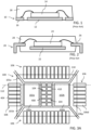
- the known Quad Flat No-Lead (QFN) package type shown in Figure 1
- the exposed device contacts of the package are provided in the form of conductive pads 16 flush with the bottom and side edges of the package housing 18 that are electrically connected to the integrated circuit die 14 through bonding wires.
- the known Quad Flat Package (QFP) package type shown in Figure 2
- the exposed device contacts of the package are provided in the form of conductive leads 26 that project from the sides of the package housing 28 that are electrically connected to the integrated circuit die 24 through bonding wires.
- the leadframe is provided with a corresponding number of dies pads and typically with a larger number of device contacts.
- Increasing the number of die pads can introduce a number of problems such as: difficulty in clamping the leadframe in order to flatten the die pads to ensure a successful bonding of the integrated circuit dies; and inability to provide a sufficient number of device contacts to handle the increased input/output complexity of supporting multiple integrated circuit dies in a single package.
- a hybrid Quad Flat No-Lead (QFN) and Quad Flat Package (QFP) integrated circuit package comprises: a leadframe including a first die pad, a second die pad, a plurality of first QFN conductive pads and a plurality of QFP conductive leads; a first integrated circuit mounted to the first die pad; a second integrated circuit mounted to the second die pad; and a package housing encapsulating the first die pad, the first integrated circuit mounted thereto, the second die pad, the second integrated circuit mounted thereto, the plurality of first QFN conductive pads, and proximal ends of the plurality of QFP conductive leads; wherein distal ends of the plurality of QFP conductive leads extend away from side edges of the package housing; and wherein bottom surfaces of the plurality of first QFN conductive pads are exposed at a bottom surface of the package housing; and wherein said plurality of first QFN conductive pads are located between the first and second die pads.
- a method of manufacturing a hybrid QFN and QFP integrated circuit package comprises: processing a metal plate to provide a proto-leadframe structure that includes a base plate and a plurality of lead structures; forming, in an upper surface of the base plate, a first die pad opening, a second die pad opening, and recesses surrounding pad structures positioned between the first and second die pad openings; mounting a first integrated circuit at the first die pad opening; mounting a second integrated circuit at the second die pad opening; encapsulating the base plate, the first integrated circuit mounted at the first die pad opening, the second integrated circuit mounted at the second die pad opening, and proximal ends of the plurality of lead structures; thinning the base plate from a backside thereof to remove material of the base plate until reaching the recesses surrounding pad structures and producing a plurality of QFN conductive pads; and processing distal ends of the lead structures to produce a plurality of QFP conductive leads.
- a hybrid QFN and QFP leadframe comprises: a base plate and a plurality of lead structures; a first die pad opening formed in an upper surface of the base plate; a second die pad opening formed in an upper surface of the base plate; and recesses formed in an upper surface of the base plate that surround pad structures positioned between the first and second die pad openings.
- Said first and second die pad openings have a first depth from a front surface of the base plate.
- Said recesses have a second depth from the front surface of the base plate. Wherein, said second depth is deeper than said first depth.
- FIGS 3A , 3B and 3C show plan (top) views of a hybrid Quad Flat No-Lead (QFN)-Quad Flat Package (QFP) leadframe 100 supporting multiple integrated circuit dies.
- the leadframe 100 includes tie bar structures 101a extending from the corners of a central region 101b.
- the leadframe 100 in Figures 3A and 3C includes two die pads 102a, 102b, a plurality of QFN conductive pads 104 and a plurality of QFP conductive leads 106.
- the leadframe 100 in Figure 3B includes three die pads 102a, 102b, 102c, a plurality of QFN conductive pads 104 and a plurality of QFP conductive leads 106.
- Each QFP conductive lead 106 includes a proximal end 106p located within the boundary of the package designated by the dotted perimeter line 110 and a distal end 106d located outside the boundary of the package. Wirebonding of the integrated circuit dies is made to the upper surfaces at the proximal ends 106p of the QFP conductive leads 106. Wirebonding of the integrated circuit dies is further made to the upper surfaces of the QFN conductive pads 104.
- the plurality of QFN conductive pads 104 are positioned between adjacent die pads 102.
- the embodiments of Figures 3A and 3B do not show the use of QFN conductive pads 104 at the boundary of the package designated by the dotted perimeter line 110.
- such placement of QFN conductive pads 104 at the package boundary in addition to placement between die pads 102a and 102b in the central region 101b, may be supported as shown, for example, in Figure 3C .
- FIG. 4 shows a cross-section of a hybrid multi-die QFP-QFN package 200.
- the cross-section of Figure 4 is taken along line 112 in Figure 3A .
- the leadframe 100 includes a first die pad 102a supporting a first integrated circuit die 224a and a second die pad 102b supporting a second integrated circuit die 224b.
- the exposed device contacts for the package 200 include QFN conductive pads 104 flush with the bottom of the package housing 218 that are electrically connected to the integrated circuit dies 224a, 224b through bonding wires and QFP conductive leads 106 that project from the sides of the package housing 228 that are electrically connected to the integrated circuit dies 224a, 224b through bonding wires.
- the bottom surfaces of the first second die pads 102a and 102b are exposed flush with the bottom of the package housing 218 in support of making electrical and/or thermal contact.
- FIG. 5 shows a cross-section of a hybrid multi-die QFP-QFN package 300.
- the cross-section of Figure 5 is taken along line 113 in Figure 3C .
- the leadframe 100 includes a first die pad 102a supporting a first integrated circuit die 224a and a second die pad 102b supporting a second integrated circuit die 224b.
- the exposed device contacts for the package 200 include QFN conductive pads 104a flush with the bottom of the package housing 218 as well as QFN conductive pads 104b flush with the bottom and side edges of the package housing 218; wherein the pads 104a, 104b are electrically connected to the integrated circuit dies 224a, 224b through bonding wires.
- the exposed device contacts for the package 200 further include QFP conductive leads 106 that project from the sides of the package housing 228; wherein the leads 106 are electrically connected to the integrated circuit dies 224a, 224b through bonding wires. It will also be noted that the bottom surfaces of the first second die pads 102a and 102b are exposed flush with the bottom of the package housing 218 in support of making electrical and/or thermal contact.
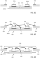
- Figures 6A-6G show steps in a method for manufacturing the hybrid multi-die QFP-QFN package.
- Figure 6A - a metal plate, for example made of copper, is processed using etching, stamping, patterning, etc., techniques as known in the art to provide a proto-leadframe structure 400 that includes a base plate 402 and a plurality of lead structures 404.
- the stamping or patterning process may be is used to define the peripheral shapes of the base plate 402 and lead structures 404.
- An etching process is used to form, in the upper surface of the base plate 402, a first die pad opening 406a, a second die pad opening 406b, and recesses 408 surrounding pad structures 410. It will be noted that the stamping process may further introduce a vertical offset of the lead structures 404 relative to the base plate 402.
- the top views of the leadframe 100 shown in Figures 3A-3C are illustrative of the leadframe configuration at this step of the process.
- Figure 6C - a die attach process is then performed to mount the first and second integrated circuit dies 224a, 224b to the base plate 402 within the first die pad opening 406a and the second die pad opening 406b, respectively.
- Figure 6D - wire bonding is then performed to electrically connect, via bonding wires 416, pads of the first and second integrated circuit dies 224a, 224b to each other, pads of the first and second integrated circuit dies 224a, 224b to the solder layer 412 at the proximal ends of the lead structures 404 and pads of the first and second integrated circuit dies 224a, 224b to the solder layer 412 at the upper surface of the pad structures 410.
- the bonding wires 416 between the first and second integrated circuit dies 224a, 224b pass over one or more of the pad structures 410.
- FIG. 6F - an etching and/or grinding process is then applied to the backside of the base plate 402 of the proto-leadframe structure 400 (and perhaps also, if needed, to the bottom portion of the package housing 228) in order to reduce the thickness of the base plate 402.
- This backside etch/grind process performed on the base plate 402 continues removing material of the base plate 402 until reaching the encapsulant material filled recesses 408 surrounding pad structures 410.
- the backside etch/grind process is continued until the insulating later 414 present at the bottom of the recesses 408 is reached and removed.
- the pad structures 410 become individually isolated to form the plurality of QFN conductive pads 104 and portions of the base plate 403 become individually isolated to form the first and second die pad 102a and 102b.
- FIG. 6G - a trimming and forming process is then performed at the distal ends 420 of the lead structures 404 to individually isolate and shape the lead structures 404 to form the plurality of QFP conductive leads 106. At this stage, the exposed ends of the tie bars 101a are also severed.
Landscapes
- Lead Frames For Integrated Circuits (AREA)
- Engineering & Computer Science (AREA)
- Microelectronics & Electronic Packaging (AREA)
Abstract
Description
- This application claims priority from
United States Provisional Application for Patent No. 63/449,366, filed March 2, 2023 - The present invention generally relates to semiconductor packaging and, more particularly, to a combined Quad Flat No-Lead (QFN) and Quad Flat Package (QFP) semiconductor package supporting multiple integrated circuit dies.
- Various kinds of packages are known in the art for semiconductor devices. The known Quad Flat No-Lead (QFN) package type, shown in
Figure 1 , is based on the use of aleadframe 10 including adie pad 12 supporting an integrated circuit die 14. The exposed device contacts of the package are provided in the form ofconductive pads 16 flush with the bottom and side edges of thepackage housing 18 that are electrically connected to the integratedcircuit die 14 through bonding wires. The known Quad Flat Package (QFP) package type, shown inFigure 2 , is also based on the use of aleadframe 20 including adie pad 22 supporting an integrated circuit die 24. However, here the exposed device contacts of the package are provided in the form of conductive leads 26 that project from the sides of thepackage housing 28 that are electrically connected to the integrated circuit die 24 through bonding wires. - It is recognized that some applications require the use of multiple integrated circuit dies within a single package. In such a case, the leadframe is provided with a corresponding number of dies pads and typically with a larger number of device contacts. Increasing the number of die pads can introduce a number of problems such as: difficulty in clamping the leadframe in order to flatten the die pads to ensure a successful bonding of the integrated circuit dies; and inability to provide a sufficient number of device contacts to handle the increased input/output complexity of supporting multiple integrated circuit dies in a single package.
- There is accordingly a need in the art to address the foregoing issues. There would be an advantage to have a semiconductor package that supports multiple integrated circuit dies and combines the use of QFN conductive pads and QFP conductive leads to provide for increased input/output complexity.
- In an embodiment, a hybrid Quad Flat No-Lead (QFN) and Quad Flat Package (QFP) integrated circuit package comprises: a leadframe including a first die pad, a second die pad, a plurality of first QFN conductive pads and a plurality of QFP conductive leads; a first integrated circuit mounted to the first die pad; a second integrated circuit mounted to the second die pad; and a package housing encapsulating the first die pad, the first integrated circuit mounted thereto, the second die pad, the second integrated circuit mounted thereto, the plurality of first QFN conductive pads, and proximal ends of the plurality of QFP conductive leads; wherein distal ends of the plurality of QFP conductive leads extend away from side edges of the package housing; and wherein bottom surfaces of the plurality of first QFN conductive pads are exposed at a bottom surface of the package housing; and wherein said plurality of first QFN conductive pads are located between the first and second die pads.
- In an embodiment, a method of manufacturing a hybrid QFN and QFP integrated circuit package comprises: processing a metal plate to provide a proto-leadframe structure that includes a base plate and a plurality of lead structures; forming, in an upper surface of the base plate, a first die pad opening, a second die pad opening, and recesses surrounding pad structures positioned between the first and second die pad openings; mounting a first integrated circuit at the first die pad opening; mounting a second integrated circuit at the second die pad opening; encapsulating the base plate, the first integrated circuit mounted at the first die pad opening, the second integrated circuit mounted at the second die pad opening, and proximal ends of the plurality of lead structures; thinning the base plate from a backside thereof to remove material of the base plate until reaching the recesses surrounding pad structures and producing a plurality of QFN conductive pads; and processing distal ends of the lead structures to produce a plurality of QFP conductive leads.
- In an embodiment, a hybrid QFN and QFP leadframe comprises: a base plate and a plurality of lead structures; a first die pad opening formed in an upper surface of the base plate; a second die pad opening formed in an upper surface of the base plate; and recesses formed in an upper surface of the base plate that surround pad structures positioned between the first and second die pad openings. Said first and second die pad openings have a first depth from a front surface of the base plate. Said recesses have a second depth from the front surface of the base plate. Wherein, said second depth is deeper than said first depth.
- For a better understanding of the embodiments, reference will now be made by way of example only to the accompanying figures in which:
-
Figure 1 shows a cross-section of a Quad Flat No-Lead (QFN) package; -
Figure 2 shows a cross-section of a Quad Flat Package (QFP) package; -
Figures 3A ,3B and 3C show plan views of a hybrid QFN-QFP leadframe supporting multiple integrated circuit dies; -
Figures 4 and 5 show cross-sections of a hybrid multi-die QFP-QFN package utilizing the leadframe shown inFigures 3A ,3B and 3C ; and -
Figures 6A-6G show steps in a method for manufacturing the hybrid multi-die QFP-QFN package. - Reference is made to
Figures 3A ,3B and 3C which show plan (top) views of a hybrid Quad Flat No-Lead (QFN)-Quad Flat Package (QFP)leadframe 100 supporting multiple integrated circuit dies. Theleadframe 100 includestie bar structures 101a extending from the corners of acentral region 101b. Theleadframe 100 inFigures 3A and3C includes twodie pads conductive pads 104 and a plurality of QFPconductive leads 106. Theleadframe 100 inFigure 3B includes threedie pads conductive pads 104 and a plurality of QFPconductive leads 106. Each QFPconductive lead 106 includes aproximal end 106p located within the boundary of the package designated by the dottedperimeter line 110 and adistal end 106d located outside the boundary of the package. Wirebonding of the integrated circuit dies is made to the upper surfaces at theproximal ends 106p of the QFPconductive leads 106. Wirebonding of the integrated circuit dies is further made to the upper surfaces of the QFNconductive pads 104. - It will be noted that in the
central region 101b for theleadframes 100 the plurality of QFNconductive pads 104 are positioned between adjacent die pads 102. For example, between diepads Figure 3A , and between diepads pads pads Figure 3B . The embodiments ofFigures 3A and3B do not show the use of QFNconductive pads 104 at the boundary of the package designated by the dottedperimeter line 110. However, it will be understood that such placement of QFNconductive pads 104 at the package boundary, in addition to placement betweendie pads central region 101b, may be supported as shown, for example, inFigure 3C . - Reference is now made to
Figure 4 which shows a cross-section of a hybrid multi-die QFP-QFN package 200. The cross-section ofFigure 4 is taken alongline 112 inFigure 3A . Theleadframe 100 includes afirst die pad 102a supporting a first integrated circuit die 224a and asecond die pad 102b supporting a second integrated circuit die 224b. The exposed device contacts for thepackage 200 include QFNconductive pads 104 flush with the bottom of thepackage housing 218 that are electrically connected to the integrated circuit dies 224a, 224b through bonding wires and QFP conductive leads 106 that project from the sides of thepackage housing 228 that are electrically connected to the integrated circuit dies 224a, 224b through bonding wires. It will also be noted that the bottom surfaces of the firstsecond die pads package housing 218 in support of making electrical and/or thermal contact. - Reference is now made to
Figure 5 which shows a cross-section of a hybrid multi-die QFP-QFN package 300. The cross-section ofFigure 5 is taken alongline 113 inFigure 3C . Theleadframe 100 includes afirst die pad 102a supporting a first integrated circuit die 224a and asecond die pad 102b supporting a second integrated circuit die 224b. The exposed device contacts for thepackage 200 include QFNconductive pads 104a flush with the bottom of thepackage housing 218 as well as QFNconductive pads 104b flush with the bottom and side edges of thepackage housing 218; wherein thepads package 200 further include QFP conductive leads 106 that project from the sides of thepackage housing 228; wherein theleads 106 are electrically connected to the integrated circuit dies 224a, 224b through bonding wires. It will also be noted that the bottom surfaces of the firstsecond die pads package housing 218 in support of making electrical and/or thermal contact. -
Figures 6A-6G show steps in a method for manufacturing the hybrid multi-die QFP-QFN package. -
Figure 6A - a metal plate, for example made of copper, is processed using etching, stamping, patterning, etc., techniques as known in the art to provide a proto-leadframe structure 400 that includes abase plate 402 and a plurality oflead structures 404. The stamping or patterning process may be is used to define the peripheral shapes of thebase plate 402 andlead structures 404. An etching process is used to form, in the upper surface of thebase plate 402, a first die pad opening 406a, a second die pad opening 406b, and recesses 408 surroundingpad structures 410. It will be noted that the stamping process may further introduce a vertical offset of thelead structures 404 relative to thebase plate 402. The top views of theleadframe 100 shown inFigures 3A-3C are illustrative of the leadframe configuration at this step of the process. -
Figure 6B - asolder layer 412 is applied at the bottom of the first die pad opening 406a, at the bottom of the second die pad opening 406b, to the upper surface of thepad structures 410, and to the upper surface oflead structures 404 at the ends thereof which are proximate to thebase plate 402. An insulating later 414 is applied at the bottom of therecesses 408. -
Figure 6C - a die attach process is then performed to mount the first and second integrated circuit dies 224a, 224b to thebase plate 402 within the first die pad opening 406a and the second die pad opening 406b, respectively. -
Figure 6D - wire bonding is then performed to electrically connect, viabonding wires 416, pads of the first and second integrated circuit dies 224a, 224b to each other, pads of the first and second integrated circuit dies 224a, 224b to thesolder layer 412 at the proximal ends of thelead structures 404 and pads of the first and second integrated circuit dies 224a, 224b to thesolder layer 412 at the upper surface of thepad structures 410. It will be noted that thebonding wires 416 between the first and second integrated circuit dies 224a, 224b pass over one or more of thepad structures 410. -
Figure 6E - the proto-leadframe structure 400 with the mounted and wire bonded first and second integrated circuit dies 224a, 224b is then placed within a molding cavity and an encapsulation material (such as a curable resin) is injected in the molding cavity to produce thepackage housing 228. This transfer molding process is well known in the art. The distal ends 420 of thelead structures 404 are clamped by the molding apparatus and thus are not encapsulated so that they will extend from the outer peripheral sides of thepackage housing 228. Thebase plate 402 of the proto-leadframe structure 400 is only partially encapsulated within thepackage housing 228; wherein a bottom portion of thebase plate 402 is exposed from thepackage housing 228. -
Figure 6F - an etching and/or grinding process is then applied to the backside of thebase plate 402 of the proto-leadframe structure 400 (and perhaps also, if needed, to the bottom portion of the package housing 228) in order to reduce the thickness of thebase plate 402. This backside etch/grind process performed on thebase plate 402 continues removing material of thebase plate 402 until reaching the encapsulant material filledrecesses 408 surroundingpad structures 410. In particular, the backside etch/grind process is continued until the insulating later 414 present at the bottom of therecesses 408 is reached and removed. At this point, thepad structures 410 become individually isolated to form the plurality of QFNconductive pads 104 and portions of the base plate 403 become individually isolated to form the first andsecond die pad -
Figure 6G - a trimming and forming process is then performed at the distal ends 420 of thelead structures 404 to individually isolate and shape thelead structures 404 to form the plurality of QFP conductive leads 106. At this stage, the exposed ends of thetie bars 101a are also severed. - While the invention has been illustrated and described in detail in the drawings and foregoing description, such illustration and description are considered illustrative or exemplary and not restrictive; the invention is not limited to the disclosed embodiments. Other variations to the disclosed embodiments can be understood and effected by those skilled in the art in practicing the claimed invention, from a study of the drawings, the disclosure, and the appended claims.
Claims (23)
- A hybrid Quad Flat No-Lead (QFN) and Quad Flat Package (QFP) integrated circuit package, comprising:a leadframe including a first die pad, a second die pad, a plurality of first QFN conductive pads and a plurality of QFP conductive leads;a first integrated circuit mounted to the first die pad;a second integrated circuit mounted to the second die pad; anda package housing encapsulating the first die pad, the first integrated circuit mounted thereto, the second die pad, the second integrated circuit mounted thereto, the plurality of first QFN conductive pads, and proximal ends of the plurality of QFP conductive leads;wherein distal ends of the plurality of QFP conductive leads extend away from side edges of the package housing; andwherein bottom surfaces of the plurality of first QFN conductive pads are exposed at a bottom surface of the package housing; andwherein said plurality of first QFN conductive pads are located between the first and second die pads.
- The hybrid QFN and QFP integrated circuit package of claim 1, wherein said leadframe further includes a plurality of second QFN conductive pads, wherein the package housing further encapsulates the plurality of second QFN conductive pads, and wherein said plurality of second QFN conductive pads are exposed at the bottom surface and at least one side edge of the package housing.
- The hybrid QFN and QFP integrated circuit package of claim 1, wherein said leadframe further includes a third die pad, further including a third integrated circuit mounted to the third die pad, wherein the package housing further encapsulates the third die pad and the third integrated circuit mounted thereto, and wherein said plurality of first QFN conductive pads are further located between the first and third die pads and between the second and third die pads.
- The hybrid QFN and QFP integrated circuit package of claim 1, further comprising wirebonds between each of the first and second integrated circuits and proximal ends of the plurality of QFP conductive leads.
- The hybrid QFN and QFP integrated circuit package of claim 4, further comprising a solder layer at upper surfaces of the plurality of first QFP conductive leads at the proximal ends thereof; wherein said wirebonds are connected to said solder layer.
- The hybrid QFN and QFP integrated circuit package of claim 1, further comprising wirebonds between each of the first and second integrated circuits and upper surfaces of the plurality of first QFN conductive pads.
- The hybrid QFN and QFP integrated circuit package of claim 6, further comprising a solder layer at upper surfaces of the plurality of first QFN conductive pads; wherein said wirebonds are connected to said solder layer.
- The hybrid QFN and QFP integrated circuit package of claim 1, further comprising wirebonds between the first and second integrated circuits that pass over on or more of the plurality of first QFN conductive pads located between the first and second die pads.
- The hybrid QFN and QFP integrated circuit package of claim 1, further comprising solder layers at surfaces of the first and second die pads; wherein said first and second integrated circuits are mounted to the solder layers.
- A method of manufacturing a hybrid Quad Flat No-Lead (QFN) and Quad Flat Package (QFP) integrated circuit package, comprising:processing a metal plate to provide a proto-leadframe structure that includes a base plate and a plurality of lead structures;forming, in an upper surface of the base plate, a first die pad opening, a second die pad opening, and recesses surrounding pad structures positioned between the first and second die pad openings;mounting a first integrated circuit at the first die pad opening;mounting a second integrated circuit at the second die pad opening;encapsulating the base plate, the first integrated circuit mounted at the first die pad opening, the second integrated circuit mounted at the second die pad opening, and proximal ends of the plurality of lead structures;thinning the base plate from a backside thereof to remove material of the base plate until reaching the recesses surrounding pad structures and producing a plurality of QFN conductive pads; andprocessing distal ends of the lead structures to produce a plurality of QFP conductive leads.
- The method of claim 10, further comprising:applying a solder layer to upper surfaces of the plurality of lead structures at the proximal ends thereof; andwirebonding one or more of the first and second integrated circuits to the solder layer at the proximal ends of the plurality of lead structures.
- The method of claim 10, further comprising:applying a solder layer to upper surfaces of the pad structures; andwirebonding one or more of the first and second integrated circuits to the solder layer at the upper surfaces of the pad structures.
- The method of claim 10, further comprising:applying a solder layer to bottoms of the first and second die pad openings; andwherein mounting the first and second integrated circuits comprises mounting to the solder layer.
- The method of claim 10, further comprising, after forming the recesses surrounding pad structures and before encapsulating the base plate, applying an insulating layer to bottoms of the recesses surrounding pad structures.
- The method of claim 14, wherein thinning the base plate is continued until the insulating layer at the bottoms of the recesses surrounding pad structures is reached.
- A hybrid Quad Flat No-Lead (QFN) and Quad Flat Package (QFP) leadframe, comprising:a base plate and a plurality of lead structures;a first die pad opening formed in an upper surface of the base plate;a second die pad opening formed in an upper surface of the base plate; andrecesses formed in an upper surface of the base plate that surround pad structures positioned between the first and second die pad openings.
- The hybrid QFN and QFP leadframe of claim 16, wherein said first and second die pad openings have a first depth from a front surface of the base plate, and wherein said recesses have a second depth from the front surface of the base plate, said second depth being deeper than said first depth.
- The hybrid QFN and QFP leadframe of claim 16, further comprising a solder layer at upper surfaces of the plurality of lead structures at proximal ends thereof.
- The hybrid QFN and QFP leadframe of claim 16, further comprising a solder layer at upper surfaces of the pad structures.
- The hybrid QFN and QFP leadframe of claim 16, further comprising a solder layer at bottoms of the first and second die pad openings.
- The hybrid QFN and QFP leadframe of claim 16, further comprising an insulating layer at bottoms of the recesses surrounding pad structures.
- The hybrid QFN and QFP leadframe of claim 16, wherein said plurality of lead structures include QFP leads and QFN pads.
- The hybrid QFN and QFP leadframe of claim 16, wherein said pad structures are configured to form QFN pads.
Applications Claiming Priority (2)
| Application Number | Priority Date | Filing Date | Title |
|---|---|---|---|
| US202363449366P | 2023-03-02 | 2023-03-02 | |
| US18/441,210 US20240297147A1 (en) | 2023-03-02 | 2024-02-14 | Hybrid multi-die qfp-qfn package |
Publications (2)
| Publication Number | Publication Date |
|---|---|
| EP4425537A2 true EP4425537A2 (en) | 2024-09-04 |
| EP4425537A3 EP4425537A3 (en) | 2024-09-25 |
Family
ID=90097449
Family Applications (1)
| Application Number | Title | Priority Date | Filing Date |
|---|---|---|---|
| EP24159904.2A Pending EP4425537A3 (en) | 2023-03-02 | 2024-02-27 | Hybrid multi-die qfp-qfn package |
Country Status (3)
| Country | Link |
|---|---|
| US (1) | US20240297147A1 (en) |
| EP (1) | EP4425537A3 (en) |
| CN (1) | CN222720429U (en) |
Families Citing this family (1)
| Publication number | Priority date | Publication date | Assignee | Title |
|---|---|---|---|---|
| US20240006278A1 (en) * | 2022-07-01 | 2024-01-04 | Mediatek Inc. | Multi-die qfn hybrid package |
Family Cites Families (1)
| Publication number | Priority date | Publication date | Assignee | Title |
|---|---|---|---|---|
| US8455988B2 (en) * | 2008-07-07 | 2013-06-04 | Stats Chippac Ltd. | Integrated circuit package system with bumped lead and nonbumped lead |
-
2024
- 2024-02-14 US US18/441,210 patent/US20240297147A1/en active Pending
- 2024-02-27 EP EP24159904.2A patent/EP4425537A3/en active Pending
- 2024-03-01 CN CN202420400965.9U patent/CN222720429U/en active Active
Also Published As
| Publication number | Publication date |
|---|---|
| US20240297147A1 (en) | 2024-09-05 |
| CN222720429U (en) | 2025-04-04 |
| EP4425537A3 (en) | 2024-09-25 |
Similar Documents
| Publication | Publication Date | Title |
|---|---|---|
| US8836101B2 (en) | Multi-chip semiconductor packages and assembly thereof | |
| TWI474455B (en) | Advanced quad flat no-lead package | |
| CN100490140C (en) | Double gauge lead frame | |
| KR100927319B1 (en) | Stamped Leadframe and Manufacturing Method Thereof | |
| US7339259B2 (en) | Semiconductor device | |
| CN100576524C (en) | Lead frame, semiconductor package and manufacturing method thereof | |
| JP2002076228A (en) | Resin-sealed semiconductor device | |
| US10707158B2 (en) | Package with vertical interconnect between carrier and clip | |
| US20050051877A1 (en) | Semiconductor package having high quantity of I/O connections and method for fabricating the same | |
| CN117558699A (en) | SMD integration on QFN via 3D stacking solution | |
| US20080188039A1 (en) | Method of fabricating chip package structure | |
| US20020149090A1 (en) | Lead frame and semiconductor package | |
| US20240297147A1 (en) | Hybrid multi-die qfp-qfn package | |
| US20150294929A1 (en) | Semiconductor die package and method of assembling same | |
| KR20040108582A (en) | Seniconductor device and method for fabricating the same | |
| US20230068748A1 (en) | Leaded semiconductor device package | |
| JPH11330314A (en) | Semiconductor device manufacturing method and structure, and lead frame used in the method | |
| CN114981940A (en) | Packaged electronic device with split die pads in a rugged package substrate | |
| JP5971531B2 (en) | Resin-sealed semiconductor device and manufacturing method thereof | |
| US10079162B1 (en) | Method for making lead frames for integrated circuit packages | |
| US20020048851A1 (en) | Process for making a semiconductor package | |
| JP2003068962A (en) | Frame for manufacturing semiconductor device and method for manufacturing semiconductor device | |
| CN119230487A (en) | QFN packaged semiconductor device and method for manufacturing the same | |
| CN118588675A (en) | Hybrid Multi-die QFP-QFN Package | |
| JP4475785B2 (en) | Manufacturing method of resin-encapsulated semiconductor device |
Legal Events
| Date | Code | Title | Description |
|---|---|---|---|
| PUAI | Public reference made under article 153(3) epc to a published international application that has entered the european phase |
Free format text: ORIGINAL CODE: 0009012 |
|
| STAA | Information on the status of an ep patent application or granted ep patent |
Free format text: STATUS: REQUEST FOR EXAMINATION WAS MADE |
|
| PUAL | Search report despatched |
Free format text: ORIGINAL CODE: 0009013 |
|
| 17P | Request for examination filed |
Effective date: 20240227 |
|
| AK | Designated contracting states |
Kind code of ref document: A2 Designated state(s): AL AT BE BG CH CY CZ DE DK EE ES FI FR GB GR HR HU IE IS IT LI LT LU LV MC ME MK MT NL NO PL PT RO RS SE SI SK SM TR |
|
| AK | Designated contracting states |
Kind code of ref document: A3 Designated state(s): AL AT BE BG CH CY CZ DE DK EE ES FI FR GB GR HR HU IE IS IT LI LT LU LV MC ME MK MT NL NO PL PT RO RS SE SI SK SM TR |
|
| RIC1 | Information provided on ipc code assigned before grant |
Ipc: H01L 23/495 20060101ALI20240821BHEP Ipc: H01L 21/48 20060101AFI20240821BHEP |