EP4425527A1 - Fuse and method for manufacturing same - Google Patents
Fuse and method for manufacturing same Download PDFInfo
- Publication number
- EP4425527A1 EP4425527A1 EP22887413.7A EP22887413A EP4425527A1 EP 4425527 A1 EP4425527 A1 EP 4425527A1 EP 22887413 A EP22887413 A EP 22887413A EP 4425527 A1 EP4425527 A1 EP 4425527A1
- Authority
- EP
- European Patent Office
- Prior art keywords
- conductive pattern
- fuse
- disposed
- film
- pcb
- Prior art date
- Legal status (The legal status is an assumption and is not a legal conclusion. Google has not performed a legal analysis and makes no representation as to the accuracy of the status listed.)
- Pending
Links
Images



Classifications
-
- H—ELECTRICITY
- H01—ELECTRIC ELEMENTS
- H01H—ELECTRIC SWITCHES; RELAYS; SELECTORS; EMERGENCY PROTECTIVE DEVICES
- H01H85/00—Protective devices in which the current flows through a part of fusible material and this current is interrupted by displacement of the fusible material when this current becomes excessive
- H01H85/02—Details
- H01H85/04—Fuses, i.e. expendable parts of the protective device, e.g. cartridges
-
- H—ELECTRICITY
- H01—ELECTRIC ELEMENTS
- H01H—ELECTRIC SWITCHES; RELAYS; SELECTORS; EMERGENCY PROTECTIVE DEVICES
- H01H85/00—Protective devices in which the current flows through a part of fusible material and this current is interrupted by displacement of the fusible material when this current becomes excessive
- H01H85/02—Details
- H01H85/04—Fuses, i.e. expendable parts of the protective device, e.g. cartridges
- H01H85/041—Fuses, i.e. expendable parts of the protective device, e.g. cartridges characterised by the type
- H01H85/046—Fuses formed as printed circuits
-
- H—ELECTRICITY
- H01—ELECTRIC ELEMENTS
- H01H—ELECTRIC SWITCHES; RELAYS; SELECTORS; EMERGENCY PROTECTIVE DEVICES
- H01H69/00—Apparatus or processes for the manufacture of emergency protective devices
- H01H69/02—Manufacture of fuses
-
- H—ELECTRICITY
- H01—ELECTRIC ELEMENTS
- H01H—ELECTRIC SWITCHES; RELAYS; SELECTORS; EMERGENCY PROTECTIVE DEVICES
- H01H69/00—Apparatus or processes for the manufacture of emergency protective devices
- H01H69/02—Manufacture of fuses
- H01H69/022—Manufacture of fuses of printed circuit fuses
-
- H—ELECTRICITY
- H05—ELECTRIC TECHNIQUES NOT OTHERWISE PROVIDED FOR
- H05K—PRINTED CIRCUITS; CASINGS OR CONSTRUCTIONAL DETAILS OF ELECTRIC APPARATUS; MANUFACTURE OF ASSEMBLAGES OF ELECTRICAL COMPONENTS
- H05K1/00—Printed circuits
- H05K1/02—Details
- H05K1/0286—Programmable, customizable or modifiable circuits
- H05K1/0293—Individual printed conductors which are adapted for modification, e.g. fusable or breakable conductors, printed switches
-
- H—ELECTRICITY
- H01—ELECTRIC ELEMENTS
- H01H—ELECTRIC SWITCHES; RELAYS; SELECTORS; EMERGENCY PROTECTIVE DEVICES
- H01H85/00—Protective devices in which the current flows through a part of fusible material and this current is interrupted by displacement of the fusible material when this current becomes excessive
- H01H85/02—Details
- H01H85/38—Means for extinguishing or suppressing arc
- H01H2085/383—Means for extinguishing or suppressing arc with insulating stationary parts
-
- H—ELECTRICITY
- H05—ELECTRIC TECHNIQUES NOT OTHERWISE PROVIDED FOR
- H05K—PRINTED CIRCUITS; CASINGS OR CONSTRUCTIONAL DETAILS OF ELECTRIC APPARATUS; MANUFACTURE OF ASSEMBLAGES OF ELECTRICAL COMPONENTS
- H05K2201/00—Indexing scheme relating to printed circuits covered by H05K1/00
- H05K2201/01—Dielectrics
- H05K2201/0104—Properties and characteristics in general
- H05K2201/012—Flame-retardant; Preventing of inflammation
-
- H—ELECTRICITY
- H05—ELECTRIC TECHNIQUES NOT OTHERWISE PROVIDED FOR
- H05K—PRINTED CIRCUITS; CASINGS OR CONSTRUCTIONAL DETAILS OF ELECTRIC APPARATUS; MANUFACTURE OF ASSEMBLAGES OF ELECTRICAL COMPONENTS
- H05K2201/00—Indexing scheme relating to printed circuits covered by H05K1/00
- H05K2201/03—Conductive materials
- H05K2201/0332—Structure of the conductor
- H05K2201/0364—Conductor shape
-
- H—ELECTRICITY
- H05—ELECTRIC TECHNIQUES NOT OTHERWISE PROVIDED FOR
- H05K—PRINTED CIRCUITS; CASINGS OR CONSTRUCTIONAL DETAILS OF ELECTRIC APPARATUS; MANUFACTURE OF ASSEMBLAGES OF ELECTRICAL COMPONENTS
- H05K2201/00—Indexing scheme relating to printed circuits covered by H05K1/00
- H05K2201/05—Flexible printed circuits [FPCs]
-
- H—ELECTRICITY
- H05—ELECTRIC TECHNIQUES NOT OTHERWISE PROVIDED FOR
- H05K—PRINTED CIRCUITS; CASINGS OR CONSTRUCTIONAL DETAILS OF ELECTRIC APPARATUS; MANUFACTURE OF ASSEMBLAGES OF ELECTRICAL COMPONENTS
- H05K2201/00—Indexing scheme relating to printed circuits covered by H05K1/00
- H05K2201/10—Details of components or other objects attached to or integrated in a printed circuit board
- H05K2201/10007—Types of components
- H05K2201/10181—Fuse
Definitions
- Embodiments disclosed herein relate to a fuse and a method of fabricating the same.
- the secondary battery refers to a rechargeable battery, and encompasses both a conventional battery such as a Ni/Cd battery and a Ni/MH battery, and a recent battery such as a lithium-ion battery.
- the lithium-ion battery has the advantage of having much higher energy density than the conventional battery such as the Ni/Cd battery and the Ni/MH battery.
- the lithium-ion battery is used as a power source for a mobile device because it can be made small and lightweight, and has recently attracted attention as a next-generation energy storage medium because its use range has been extended even to power sources for electric vehicles.
- a fuse In a battery sensing line, a fuse is used to prevent fire and the like problems that may occur due to high voltage.
- a sensing line on a printed circuit board (PCB) employs a conductive pattern in the form of accumulating heat, a burn mark is generated in an upper film at a temperature where the conductive pattern works and may make it difficult to secure sufficient insulation resistance even after the conductive pattern is broken.
- An aspect of embodiments disclosed herein is to provide a fuse, in which a burn mark is less generated in a film on a conductive pattern, and a method of fabricating the same.
- An aspect of embodiments disclosed herein is to provide a fuse, in which a film on a conductive pattern is opened to prevent a phenomenon that insulation resistance decreases and to prevent a phenomenon that the conductive pattern swells up in its upper portion by gas generated therein when working, and a method of fabricating the same.
- a fuse according to an embodiment disclosed herein includes a printed circuit board (PCB); a conductive pattern disposed on the PCB; a film disposed at opposite lateral sides of the conductive pattern or on the conductive pattern to open at least a partial region above the conductive pattern; and a coating disposed on the conductive pattern and the film.
- PCB printed circuit board
- a conductive pattern disposed on the PCB
- a film disposed at opposite lateral sides of the conductive pattern or on the conductive pattern to open at least a partial region above the conductive pattern
- a coating disposed on the conductive pattern and the film.
- the coating may include a flame-retardant material.
- the flame-retardant material may contain a flam-retardant substance of a V0 rating.
- the at least a partially opened region may have a rectangular or circular shape.
- the conductive pattern may be formed in zigzags on the PCB to accumulate heat.
- the film may be disposed being spaced at a distance from the conductive pattern at opposite lateral sides of the conductive pattern.
- the film may be disposed to at least partially cover opposite upper portions of the conductive pattern.
- the coating may have adhesive strength set to be physically spaced apart from the conductive pattern upon generating gas between the conductive pattern and the coating.
- the fuse may further include a dummy region disposed on the film and limiting heat dissipation.
- the dummy region may contain copper.
- the dummy region may be disposed in a region other than a region above a melting and breaking portion of the conductive pattern.
- a method of fabricating a fuse includes forming a conductive pattern disposed on a printed circuit board (PCB); forming a film disposed at opposite lateral sides of the conductive pattern or on the conductive pattern to open at least a partial region above the conductive pattern; and forming a coating disposed on the conductive pattern and the film.
- PCB printed circuit board
- a partial region above a conductive pattern is opened to prevent a phenomenon that a burn mark is generated in a film and insulation resistance decreases.
- an opened region above a conductive pattern is minimized to provide a stable structure for preventing the conductive pattern from moving.
- a coating having a high flame-retardant rating is used to prevent a fire from breaking out in a PCB when a conductive pattern works.
- the adhesive strength of a coating is set to physically space the conductive pattern and the coating from each other when the conductive pattern works.
- a dummy is used on the film to minimize heat dissipation in a region desired to be broken.
- FIG. 1 illustrates a fuse according to an embodiment disclosed herein.
- the fuse 100 may include a printed circuit board (PCB) 110, a conductive pattern 120, a film 130, and a coating 140.
- PCB printed circuit board
- the PCB 110 may include a PCB or a flexible printed circuit board (FPCB).
- FPCB flexible printed circuit board
- the conductive pattern 120 may be disposed on the PCB 110.
- the conductive pattern 120 may be formed in zigzags on the PCB 110 so as to accumulate heat.
- the conductive pattern 120 may contain copper.
- the conductive pattern 120 may work at a temperature of 1,040 degrees or higher.
- the conductive pattern 120 may be melt at a set temperature or higher.
- the film 130 may be disposed at opposite lateral sides of the conductive pattern 120 or disposed on the conductive pattern 120.
- the film 130 may be disposed to open at least a partial region above the conductive pattern 120.
- the film 130 may be disposed being spaced at a distance from the conductive pattern 120 at both lateral sides of the conductive pattern 120.
- the film 130 is disposed to open at least a partial region above the conductive pattern 120, a burn mark may not be formed even when high heat is generated while the conductive pattern 120 is being broken.
- at least a partial region opened on the conductive pattern 120 may be shaped like any one of a quadrangle, a circle, and a polygon.
- the coating 140 may be disposed on the conductive pattern 120 and the film 130.
- the coating 140 may contain a flame-retardant material.
- the flame-retardant material may include a flame-retardant substance of a V0 rating.
- the coating 140 can prevent fire (or flame) even though high heat is generated while the conductive pattern 120 is working.
- the coating 140 can cover at least a partial region, opened by the film 130, on the conductive pattern 120
- the coating 140 may contain a material having low heat-absorption properties.
- the coating 140 may employ a material having low heat-absorption properties so that the conductive pattern 120 can be easily broken in a region where the coating 140 is in contact with the conductive pattern 120.
- an upper portion of the conductive pattern 120 may swell up due to gas generated therein.
- the coating 140 covering the upper portion of the conductive pattern 120 may prevent the upper portion of the conductive pattern 120 from swelling up.
- the coating 140 may have adhesive strength set to be physically spaced apart from the conductive pattern 120 when gas is generated between the conductive pattern 120 and the coating 140. For example, when an overcurrent flows in the conductive pattern 120, heat may be transferred to the film 130 and adhesive, thereby generating gas and causing a space between the conductive pattern 120 and the coating 140. To prevent the space due to the gas, the conductive pattern 120 needs to work quickly, and thus the adhesive strength of the coating 140 is set to physically space the coating 140 from the conductive pattern 120 when the overcurrent flows in the conductive pattern 120.
- the film 130 or the coating 140 may cover the upper portion of the conductive pattern 120, thereby providing a stable structure for preventing the conductive pattern 120 from moving.
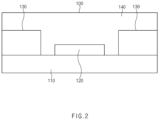
- FIG. 2 is a block diagram illustrating a cross-section of a fuse according to an embodiment disclosed herein.
- the PCB 110 may be disposed beneath the fuse 100.
- the conductive pattern 120 may be disposed on the PCB 110. According to an embodiment, the film or the adhesive may be further provided between the PCB 110 and the conductive pattern 120.
- the film 130 may be attached to the top of the PCB 110, and disposed to open at least a partial region above the conductive pattern 120.
- FIG. 2 shows an example that the film 130 is disposed to open the whole region above the conductive pattern 120, but the embodiment is not limited thereto.
- the film 130 may be disposed at both lateral sides of the conductive pattern 120.
- the film 130 may be disposed being spaced at a distance from the conductive pattern 120 at both lateral sides of the conductive pattern 120.
- the coating 140 may be disposed to cover the upper portion of the conductive pattern 120 and the film 130.
- the coating 140 may cover the upper portion of the conductive pattern 120 in the region where the upper portion of the conductive pattern 120 is not covered with the film 130.
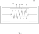
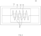
- FIGS. 3 to 5 are views illustrating an example that an upper portion of a fuse according to an embodiment disclosed herein is opened.
- the film 130 included in the fuse 100 may be disposed to open at least a partial region 10 above the conductive pattern 120.
- the film 130 may be disposed to open at least a partial region 10 above the conductive pattern 120, and the coating 140 may be disposed to cover the film 130 and the conductive pattern 120.
- the partially opened region 10 above the conductive pattern 120 has a rectangular shape.
- the conductive pattern 120 may move and short-circuit again even after the conductive pattern 120 works to be broken. Therefore, it is required to minimize the partially opened region 10.
- the film 130 included in the fuse 100 may open at least a partial region 20 above the conductive pattern 120.
- the at least a partial region 20 may have a quadrangular shape.
- the at least partially opened regions 20 may include a plurality of rectangular regions.
- the film 130 may open a partial region above the conductive pattern 120 through the plurality of rectangular regions.
- the film 130 included in the fuse 100 may open at least a partial region 20 above the conductive pattern 120.
- the at least a partial region 20 may have a circular shape.
- the at least partially opened regions 20 may include a plurality of circular regions.
- the film 130 may open a partial region above the conductive pattern 120 through the plurality of circular regions.
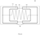
- FIG. 6 is a view illustrating a dummy region of a fuse according to an embodiment disclosed herein.
- the fuse 100 may further include a dummy region 150.
- the dummy region 150 may be disposed on the film 130.
- the dummy region 150 may be disposed on the film 130 to limit heat dissipation.
- the dummy region 150 may be disposed on the film 130 to minimize the heat dissipation.
- the film 130 may be disposed on the conductive pattern 120, and the dummy region 150 may be disposed on the film 130 and protect the film 130 because the film 130 alone is weak and easy to tear.
- the dummy region 150 may contain copper.
- the dummy region 150 may be disposed in a region other than a region above a melting and breaking portion of the conductive pattern 120.
- the dummy region 150 may be deleted or minimized above the melting and breaking portion of the conductive pattern 120, thereby minimizing heat dissipation. Therefore, the melting and breaking portion of the conductive pattern 120 is highly likely to be broken.
- the dummy region 150 may have a shape as shown in FIG. 6 .
- the dummy region 150 is not limited to this shape, but may have various shapes as long as it is disposed on the film 130 and not disposed above the melting and breaking portion of the conductive pattern 120.
- FIG. 7 illustrates a cross-section of a fuse according to another embodiment disclosed herein.
- a fuse 200 may include a PCB 210, a conductive pattern 220, a film 230, and a coating 240.
- the PCB 210, the conductive pattern 220, the film 230, and the coating 240 may be substantially the same as the PCB 110, the conductive pattern 120, the film 130 and the coating 140 shown in FIG. 1 .
- the film 230 may be disposed on the conductive pattern 220 to open a least a partial region above the conductive pattern 220.
- the film 230 may be disposed to cover opposite upper portions of the conductive pattern 220.
- the coating 240 may cover the film 230 and the conductive pattern 220.
- At least a partial region above the conductive pattern 220 of the fuse 200 shown in FIG. 7 may be opened by the film 230 like that shown in FIGS. 3 to 5 .
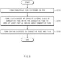
- FIG. 8 is a flowchart showing a method of fabricating a fuse according to an embodiment disclosed herein.
- the method of fabricating the fuse 100 may include steps of forming a conductive pattern disposed on the PCB (S110), forming a film disposed at opposite lateral sides of the conductive pattern or on the conductive pattern to open at least a partial region above the conductive pattern (S120), and forming a coating disposed on the conductive pattern and the film (S130).
- the conductive pattern 120 may be formed to be disposed on the PCB 110.
- the conductive pattern 120 may be formed in zigzags on the PCB 110 so as to accumulate heat of the PCB 110.
- the film 130 may be formed to open at least a partial region above the conductive pattern 120.
- the film 130 may be disposed at both lateral sides of the conductive pattern 120 or on the conductive pattern 120.
- the film 130 may open at least a partial region above the conductive pattern 120 in a rectangular or circular shape.
- the coating 140 may be formed on the conductive pattern 120 and the film 130.
- the coating 140 may include a flame-retardant material, and the flame-retardant material may include a flame-retardant substance of a V0 rating.
- the coating 140 may have adhesive strength set to be physically spaced apart from the conductive pattern 120 when gas is generated between the conductive pattern 120 and the coating 140
Landscapes
- Engineering & Computer Science (AREA)
- Manufacturing & Machinery (AREA)
- Microelectronics & Electronic Packaging (AREA)
- Fuses (AREA)
Abstract
Description
- This application claims the priority benefit of the priority based on
Korean Patent Application No. 10-2021-0147220, filed October 29, 2021 - Embodiments disclosed herein relate to a fuse and a method of fabricating the same.
- Recently, research and development on secondary batteries has been actively conducted. Here, the secondary battery refers to a rechargeable battery, and encompasses both a conventional battery such as a Ni/Cd battery and a Ni/MH battery, and a recent battery such as a lithium-ion battery. Among the secondary batteries, the lithium-ion battery has the advantage of having much higher energy density than the conventional battery such as the Ni/Cd battery and the Ni/MH battery. Further, the lithium-ion battery is used as a power source for a mobile device because it can be made small and lightweight, and has recently attracted attention as a next-generation energy storage medium because its use range has been extended even to power sources for electric vehicles.
- In a battery sensing line, a fuse is used to prevent fire and the like problems that may occur due to high voltage. When a sensing line on a printed circuit board (PCB) employs a conductive pattern in the form of accumulating heat, a burn mark is generated in an upper film at a temperature where the conductive pattern works and may make it difficult to secure sufficient insulation resistance even after the conductive pattern is broken.
- An aspect of embodiments disclosed herein is to provide a fuse, in which a burn mark is less generated in a film on a conductive pattern, and a method of fabricating the same.
- An aspect of embodiments disclosed herein is to provide a fuse, in which a film on a conductive pattern is opened to prevent a phenomenon that insulation resistance decreases and to prevent a phenomenon that the conductive pattern swells up in its upper portion by gas generated therein when working, and a method of fabricating the same.
- Technical problems of embodiments disclosed herein are not limited to the forementioned technical problems, and other unmentioned technical problems can be clearly understood from the following descriptions by those skilled in art.
- A fuse according to an embodiment disclosed herein includes a printed circuit board (PCB); a conductive pattern disposed on the PCB; a film disposed at opposite lateral sides of the conductive pattern or on the conductive pattern to open at least a partial region above the conductive pattern; and a coating disposed on the conductive pattern and the film.
- According to an embodiment, the coating may include a flame-retardant material.
- According to an embodiment, the flame-retardant material may contain a flam-retardant substance of a V0 rating.
- According to an embodiment, the at least a partially opened region may have a rectangular or circular shape.
- According to an embodiment, the conductive pattern may be formed in zigzags on the PCB to accumulate heat.
- According to an embodiment, the film may be disposed being spaced at a distance from the conductive pattern at opposite lateral sides of the conductive pattern.
- According to an embodiment, the film may be disposed to at least partially cover opposite upper portions of the conductive pattern.
- According to an embodiment, the coating may have adhesive strength set to be physically spaced apart from the conductive pattern upon generating gas between the conductive pattern and the coating.
- According to an embodiment, the fuse may further include a dummy region disposed on the film and limiting heat dissipation.
- According to an embodiment, the dummy region may contain copper.
- According to an embodiment, the dummy region may be disposed in a region other than a region above a melting and breaking portion of the conductive pattern.
- A method of fabricating a fuse according to an embodiment disclosed herein includes forming a conductive pattern disposed on a printed circuit board (PCB); forming a film disposed at opposite lateral sides of the conductive pattern or on the conductive pattern to open at least a partial region above the conductive pattern; and forming a coating disposed on the conductive pattern and the film.
- In a fuse and a method of fabricating the same according to an embodiment disclosed herein, a partial region above a conductive pattern is opened to prevent a phenomenon that a burn mark is generated in a film and insulation resistance decreases.
- In a fuse and a method of fabricating the same according to an embodiment disclosed herein, it is possible to prevent a phenomenon that an upper portion of a conductive pattern swells up due to gas generated therein when the conductive pattern works.
- In a fuse and a method of fabricating the same according to an embodiment disclosed herein, an opened region above a conductive pattern is minimized to provide a stable structure for preventing the conductive pattern from moving.
- In a fuse and a method of fabricating the same according to an embodiment disclosed herein, a coating having a high flame-retardant rating is used to prevent a fire from breaking out in a PCB when a conductive pattern works.
- In a fuse and a method of fabricating the same according to an embodiment disclosed herein, the adhesive strength of a coating is set to physically space the conductive pattern and the coating from each other when the conductive pattern works.
- In a fuse and a method of fabricating the same according to an embodiment disclosed herein, a dummy is used on the film to minimize heat dissipation in a region desired to be broken.
- Besides, various effects directly or indirectly ascertained through the disclosure may be provided.
-
-
FIG. 1 illustrates a fuse according to an embodiment disclosed herein. -
FIG. 2 is a block diagram illustrating a cross-section of a fuse according to an embodiment disclosed herein. -
FIGS. 3 to 5 are views illustrating an example that an upper portion of a fuse according to an embodiment disclosed herein is opened. -
FIG. 6 is a view illustrating a dummy region of a fuse according to an embodiment disclosed herein. -
FIG. 7 is a view illustrating a cross-section of a fuse according to another embodiment disclosed herein. -
FIG. 8 is a flowchart showing a method of fabricating a fuse according to an embodiment disclosed herein. - Hereinafter, embodiments disclosed herein will be described in detail with reference to the accompanying drawings. It should be noted that, in adding reference numerals to the elements in the drawings, like reference numerals designate like elements, even though the elements are shown in different drawings. Further, in describing the embodiments disclosed herein, a detailed description of related well-known features or functions herein may be omitted to avoid obscuring the embodiments disclosed herein.
- In describing the elements of the embodiments disclosed herein, terms such as first, second, A, B, (a), (b), and the like may be used. These terms are merely intended to distinguish one element from another element, and the terms do not limit the nature, sequence or order of the elements. Unless otherwise defined, all terms used herein, including technical or scientific terms, have the same meanings as those generally understood by a person having ordinary knowledge in the art to which the embodiments disclosed herein pertain. Such terms as those defined in a generally used dictionary are to be interpreted as having meanings equal to the contextual meanings in the relevant field of art, and are not to be interpreted as having ideal or excessively formal meanings unless clearly defined as having such in the present application.
-
FIG. 1 illustrates a fuse according to an embodiment disclosed herein. - Referring to
FIG. 1 , thefuse 100 according to an embodiment disclosed herein may include a printed circuit board (PCB) 110, aconductive pattern 120, afilm 130, and acoating 140. - The PCB 110 may include a PCB or a flexible printed circuit board (FPCB).
- The
conductive pattern 120 may be disposed on thePCB 110. For example, theconductive pattern 120 may be formed in zigzags on thePCB 110 so as to accumulate heat. As another example, theconductive pattern 120 may contain copper. In this case, theconductive pattern 120 may work at a temperature of 1,040 degrees or higher. As another example, theconductive pattern 120 may be melt at a set temperature or higher. - The
film 130 may be disposed at opposite lateral sides of theconductive pattern 120 or disposed on theconductive pattern 120. Thefilm 130 may be disposed to open at least a partial region above theconductive pattern 120. For example, thefilm 130 may be disposed being spaced at a distance from theconductive pattern 120 at both lateral sides of theconductive pattern 120. According to an embodiment, thefilm 130 is disposed to open at least a partial region above theconductive pattern 120, a burn mark may not be formed even when high heat is generated while theconductive pattern 120 is being broken. According to an embodiment, at least a partial region opened on theconductive pattern 120 may be shaped like any one of a quadrangle, a circle, and a polygon. - The
coating 140 may be disposed on theconductive pattern 120 and thefilm 130. For example, thecoating 140 may contain a flame-retardant material. According to an embodiment, the flame-retardant material may include a flame-retardant substance of a V0 rating. In other words, thecoating 140 can prevent fire (or flame) even though high heat is generated while theconductive pattern 120 is working. Thecoating 140 can cover at least a partial region, opened by thefilm 130, on theconductive pattern 120 - The
coating 140 may contain a material having low heat-absorption properties. For example, thecoating 140 may employ a material having low heat-absorption properties so that theconductive pattern 120 can be easily broken in a region where thecoating 140 is in contact with theconductive pattern 120. - When the
conductive pattern 120 works, an upper portion of theconductive pattern 120 may swell up due to gas generated therein. At this time, thecoating 140 covering the upper portion of theconductive pattern 120 may prevent the upper portion of theconductive pattern 120 from swelling up. - According to an embodiment, the
coating 140 may have adhesive strength set to be physically spaced apart from theconductive pattern 120 when gas is generated between theconductive pattern 120 and thecoating 140. For example, when an overcurrent flows in theconductive pattern 120, heat may be transferred to thefilm 130 and adhesive, thereby generating gas and causing a space between theconductive pattern 120 and thecoating 140. To prevent the space due to the gas, theconductive pattern 120 needs to work quickly, and thus the adhesive strength of thecoating 140 is set to physically space thecoating 140 from theconductive pattern 120 when the overcurrent flows in theconductive pattern 120. - According to an embodiment, the
film 130 or thecoating 140 may cover the upper portion of theconductive pattern 120, thereby providing a stable structure for preventing theconductive pattern 120 from moving. -
FIG. 2 is a block diagram illustrating a cross-section of a fuse according to an embodiment disclosed herein. - Referring to
FIG. 2 , thePCB 110 may be disposed beneath thefuse 100. - The
conductive pattern 120 may be disposed on thePCB 110. According to an embodiment, the film or the adhesive may be further provided between thePCB 110 and theconductive pattern 120. - The
film 130 may be attached to the top of thePCB 110, and disposed to open at least a partial region above theconductive pattern 120.FIG. 2 shows an example that thefilm 130 is disposed to open the whole region above theconductive pattern 120, but the embodiment is not limited thereto. - The
film 130 may be disposed at both lateral sides of theconductive pattern 120. For example, thefilm 130 may be disposed being spaced at a distance from theconductive pattern 120 at both lateral sides of theconductive pattern 120. - The
coating 140 may be disposed to cover the upper portion of theconductive pattern 120 and thefilm 130. For example, thecoating 140 may cover the upper portion of theconductive pattern 120 in the region where the upper portion of theconductive pattern 120 is not covered with thefilm 130. -
FIGS. 3 to 5 are views illustrating an example that an upper portion of a fuse according to an embodiment disclosed herein is opened. - Referring to
FIG. 3 , thefilm 130 included in thefuse 100 according to an embodiment disclosed herein may be disposed to open at least apartial region 10 above theconductive pattern 120. For example, thefilm 130 may be disposed to open at least apartial region 10 above theconductive pattern 120, and thecoating 140 may be disposed to cover thefilm 130 and theconductive pattern 120. - The partially opened
region 10 above theconductive pattern 120 has a rectangular shape. The larger the partially openedregion 10, the more difficult it is to fix and stabilize theconductive pattern 120. In other words, when the partially openedregion 10 is large, theconductive pattern 120 may move and short-circuit again even after theconductive pattern 120 works to be broken. Therefore, it is required to minimize the partially openedregion 10. - Referring to
FIG. 4 , thefilm 130 included in thefuse 100 according to an embodiment disclosed herein may open at least apartial region 20 above theconductive pattern 120. For example, the at least apartial region 20 may have a quadrangular shape. - There may be a plurality of at least partially opened
regions 20 above theconductive pattern 120. For example, as shown inFIG. 4 , the at least partially openedregions 20 may include a plurality of rectangular regions. As another example, to minimize the partially openedregion 20 above theconductive pattern 120, thefilm 130 may open a partial region above theconductive pattern 120 through the plurality of rectangular regions. - Referring to
FIG. 5 , thefilm 130 included in thefuse 100 according to an embodiment disclosed herein may open at least apartial region 20 above theconductive pattern 120. For example, the at least apartial region 20 may have a circular shape. - There may be a plurality of at least partially opened
regions 20 above theconductive pattern 120. For example, as shown inFIG. 4 , the at least partially openedregions 20 may include a plurality of circular regions. As another example, to minimize the partially openedregion 20 above theconductive pattern 120, thefilm 130 may open a partial region above theconductive pattern 120 through the plurality of circular regions. -
FIG. 6 is a view illustrating a dummy region of a fuse according to an embodiment disclosed herein. - Referring to
FIG. 6 , thefuse 100 according to an embodiment disclosed herein may further include adummy region 150. - The
dummy region 150 may be disposed on thefilm 130. For example, thedummy region 150 may be disposed on thefilm 130 to limit heat dissipation. As another example, thedummy region 150 may be disposed on thefilm 130 to minimize the heat dissipation. Thefilm 130 may be disposed on theconductive pattern 120, and thedummy region 150 may be disposed on thefilm 130 and protect thefilm 130 because thefilm 130 alone is weak and easy to tear. According to an embodiment, thedummy region 150 may contain copper. - The
dummy region 150 may be disposed in a region other than a region above a melting and breaking portion of theconductive pattern 120. For example, thedummy region 150 may be deleted or minimized above the melting and breaking portion of theconductive pattern 120, thereby minimizing heat dissipation. Therefore, the melting and breaking portion of theconductive pattern 120 is highly likely to be broken. - According to an embodiment, the
dummy region 150 may have a shape as shown inFIG. 6 . However, thedummy region 150 is not limited to this shape, but may have various shapes as long as it is disposed on thefilm 130 and not disposed above the melting and breaking portion of theconductive pattern 120. -
FIG. 7 illustrates a cross-section of a fuse according to another embodiment disclosed herein. - Referring to
FIG. 7 , afuse 200 according to another embodiment disclosed herein may include aPCB 210, aconductive pattern 220, afilm 230, and acoating 240. According to an embodiment, thePCB 210, theconductive pattern 220, thefilm 230, and thecoating 240 may be substantially the same as thePCB 110, theconductive pattern 120, thefilm 130 and thecoating 140 shown inFIG. 1 . - The
film 230 may be disposed on theconductive pattern 220 to open a least a partial region above theconductive pattern 220. For example, thefilm 230 may be disposed to cover opposite upper portions of theconductive pattern 220. - The
coating 240 may cover thefilm 230 and theconductive pattern 220. - According to an embodiment, at least a partial region above the
conductive pattern 220 of thefuse 200 shown inFIG. 7 may be opened by thefilm 230 like that shown inFIGS. 3 to 5 . -
FIG. 8 is a flowchart showing a method of fabricating a fuse according to an embodiment disclosed herein. - Referring to
FIG. 8 , the method of fabricating thefuse 100 according to an embodiment disclosed herein may include steps of forming a conductive pattern disposed on the PCB (S110), forming a film disposed at opposite lateral sides of the conductive pattern or on the conductive pattern to open at least a partial region above the conductive pattern (S120), and forming a coating disposed on the conductive pattern and the film (S130). - In step S110 of forming the conductive pattern disposed on the PCB, the
conductive pattern 120 may be formed to be disposed on thePCB 110. For example, theconductive pattern 120 may be formed in zigzags on thePCB 110 so as to accumulate heat of thePCB 110. - In step S120 of forming the film disposed at both lateral sides of the conductive pattern or on the conductive pattern to open at least a partial region above the conductive pattern, the
film 130 may be formed to open at least a partial region above theconductive pattern 120. For example, thefilm 130 may be disposed at both lateral sides of theconductive pattern 120 or on theconductive pattern 120. As another example, thefilm 130 may open at least a partial region above theconductive pattern 120 in a rectangular or circular shape. - In step S130 of forming a coating disposed on the conductive pattern and the film, the
coating 140 may be formed on theconductive pattern 120 and thefilm 130. For example, thecoating 140 may include a flame-retardant material, and the flame-retardant material may include a flame-retardant substance of a V0 rating. As another example, thecoating 140 may have adhesive strength set to be physically spaced apart from theconductive pattern 120 when gas is generated between theconductive pattern 120 and thecoating 140 - The foregoing description is merely illustrative of the technical idea disclosed herein, and various modifications and variations will be possible without departing from the essential characteristics of the embodiments disclosed herein by a person having ordinary knowledge in the art to which the embodiments disclosed herein pertain.
- Therefore, the embodiments disclosed herein are intended for description rather than limitation of the technical spirit of the embodiments disclosed herein and the scope of the technical spirit disclosed herein is not limited by these embodiments. The protection scope of the technical spirit disclosed herein should be interpreted by the following claims, and all technical spirits within the same range should be understood to be included in the range of this document.
Claims (13)
- A fuse comprising:a printed circuit board (PCB);a conductive pattern disposed on the PCB;a film disposed at opposite lateral sides of the conductive pattern or on the conductive pattern to open at least a partial region above the conductive pattern; anda coating disposed on the conductive pattern and the film.
- The fuse of claim 1, wherein the coating comprises a flame-retardant material.
- The fuse of claim 2, wherein the flame-retardant material contains a flam-retardant substance of a V0 rating.
- The fuse of claim 1, wherein the at least a partially opened region has a rectangular or circular shape.
- The fuse of claim 1, wherein the conductive pattern is formed in zigzags on the PCB to accumulate heat.
- The fuse of claim 1, wherein the film is disposed being spaced at a distance from the conductive pattern at opposite lateral sides of the conductive pattern.
- The fuse of claim 1, wherein the film is disposed to at least partially cover opposite upper portions of the conductive pattern.
- The fuse of claim 1, wherein the coating has adhesive strength set to be physically spaced apart from the conductive pattern upon generating gas between the conductive pattern and the coating.
- The fuse of claim 1, further comprising a dummy region disposed on the film and limiting heat dissipation.
- The fuse of claim 9, wherein the dummy region contains copper.
- The fuse of claim 9, wherein the dummy region is disposed in a region other than a region above a melting and breaking portion of the conductive pattern.
- The fuse of claim 1, wherein the PCB comprises a PCB or a flexible printed circuit board (FPCB).
- A method of fabricating a fuse, comprising:forming a conductive pattern disposed on a printed circuit board (PCB);forming a film disposed at opposite lateral sides of the conductive pattern or on the conductive pattern to open at least a partial region above the conductive pattern; andforming a coating disposed on the conductive pattern and the film.
Applications Claiming Priority (2)
| Application Number | Priority Date | Filing Date | Title |
|---|---|---|---|
| KR1020210147220A KR102940890B1 (en) | 2021-10-29 | 2021-10-29 | Fuse and manufacturing method of the same |
| PCT/KR2022/015309 WO2023075210A1 (en) | 2021-10-29 | 2022-10-11 | Fuse and method for manufacturing same |
Publications (2)
| Publication Number | Publication Date |
|---|---|
| EP4425527A1 true EP4425527A1 (en) | 2024-09-04 |
| EP4425527A4 EP4425527A4 (en) | 2025-01-22 |
Family
ID=86158055
Family Applications (1)
| Application Number | Title | Priority Date | Filing Date |
|---|---|---|---|
| EP22887413.7A Pending EP4425527A4 (en) | 2021-10-29 | 2022-10-11 | SECURITY AND METHOD FOR PRODUCING SAME |
Country Status (6)
| Country | Link |
|---|---|
| US (1) | US20240429013A1 (en) |
| EP (1) | EP4425527A4 (en) |
| JP (1) | JP7855821B2 (en) |
| KR (1) | KR102940890B1 (en) |
| CN (1) | CN117882166A (en) |
| WO (1) | WO2023075210A1 (en) |
Cited By (1)
| Publication number | Priority date | Publication date | Assignee | Title |
|---|---|---|---|---|
| EP4319501A4 (en) * | 2022-02-16 | 2024-11-13 | Lg Energy Solution, Ltd. | PATTERN FUSE COMPRISING AN OPENING, AND BATTERY MODULE COMPRISING SAME |
Family Cites Families (22)
| Publication number | Priority date | Publication date | Assignee | Title |
|---|---|---|---|---|
| JPS60143544A (en) * | 1983-12-29 | 1985-07-29 | 松下電器産業株式会社 | Chip-shaped fuse |
| JPH09115413A (en) * | 1995-10-18 | 1997-05-02 | Matsushita Electric Ind Co Ltd | Chip type fuse resistor and method of manufacturing the same |
| JPH10302605A (en) * | 1997-04-25 | 1998-11-13 | Hitachi Chem Co Ltd | Chip fuse and manufacture thereof |
| US7489229B2 (en) * | 2001-06-11 | 2009-02-10 | Wickmann-Werke Gmbh | Fuse component |
| KR101361828B1 (en) * | 2007-09-03 | 2014-02-12 | 삼성전자주식회사 | Semiconductor device, Semiconductor package, stacked module, card, system and method of the semiconductor device |
| KR101050007B1 (en) * | 2008-11-03 | 2011-07-19 | 율촌화학 주식회사 | Cell packaging material and manufacturing method |
| JP5212994B2 (en) * | 2010-09-02 | 2013-06-19 | 大東通信機株式会社 | Current fuse |
| JP5546406B2 (en) * | 2010-09-28 | 2014-07-09 | 京セラ株式会社 | Ceramic fuse and ceramic fuse substrate |
| KR20120047516A (en) * | 2010-11-04 | 2012-05-14 | 에스케이하이닉스 주식회사 | Fuse in semiconductor device and method for manufacturing the same |
| DE102010063832B4 (en) * | 2010-12-22 | 2020-08-13 | Tridonic Gmbh & Co Kg | Circuit protection, circuit board and operating circuit for lamps with the circuit protection |
| CN203761658U (en) * | 2014-03-31 | 2014-08-06 | 厦门赛尔特电子有限公司 | Optical controller with surge protecting function |
| JP6453720B2 (en) * | 2015-06-24 | 2019-01-16 | 住友電気工業株式会社 | Flexible printed wiring board |
| EP3389077B1 (en) * | 2017-04-10 | 2020-01-29 | Fibar Group S.A. | Printed circuit fuse and method for use of the same |
| CN107464732B (en) * | 2017-09-11 | 2020-01-03 | 南京萨特科技发展有限公司 | PCB matrix fuse and manufacturing method thereof |
| KR102187077B1 (en) * | 2018-12-28 | 2020-12-04 | 주식회사 유라코퍼레이션 | Printed Circuit Board |
| KR102274251B1 (en) * | 2019-01-22 | 2021-07-07 | 주식회사 아모그린텍 | Thermal fusible Heating element and heater unit including the same |
| JP6887696B2 (en) * | 2019-11-12 | 2021-06-16 | ジンヨングローバル カンパニーリミテッド | Fuse element, flexible wiring board and battery pack |
| KR20210081819A (en) * | 2019-12-24 | 2021-07-02 | 한국단자공업 주식회사 | Pattern fuse and circuit board having the same |
| JP2021111523A (en) * | 2020-01-10 | 2021-08-02 | 株式会社豊田自動織機 | Power storage module and manufacturing method of flexible printed circuit board |
| KR20210147220A (en) | 2020-05-28 | 2021-12-07 | 주식회사 우진산전 | System and automatical operation method of Micro-grid connected to weak grid |
| WO2023075200A1 (en) * | 2021-10-28 | 2023-05-04 | 주식회사 엘지에너지솔루션 | Pattern fuse and method for manufacturing same |
| KR102755809B1 (en) * | 2022-02-16 | 2025-01-21 | 주식회사 엘지에너지솔루션 | Pattern fuse including opening and battery module including same |
-
2021
- 2021-10-29 KR KR1020210147220A patent/KR102940890B1/en active Active
-
2022
- 2022-10-11 EP EP22887413.7A patent/EP4425527A4/en active Pending
- 2022-10-11 CN CN202280058654.2A patent/CN117882166A/en active Pending
- 2022-10-11 US US18/689,115 patent/US20240429013A1/en active Pending
- 2022-10-11 JP JP2024518529A patent/JP7855821B2/en active Active
- 2022-10-11 WO PCT/KR2022/015309 patent/WO2023075210A1/en not_active Ceased
Cited By (2)
| Publication number | Priority date | Publication date | Assignee | Title |
|---|---|---|---|---|
| EP4319501A4 (en) * | 2022-02-16 | 2024-11-13 | Lg Energy Solution, Ltd. | PATTERN FUSE COMPRISING AN OPENING, AND BATTERY MODULE COMPRISING SAME |
| US12437951B2 (en) | 2022-02-16 | 2025-10-07 | Lg Energy Solution, Ltd. | Pattern fuse including opening and battery module including the same |
Also Published As
| Publication number | Publication date |
|---|---|
| CN117882166A (en) | 2024-04-12 |
| US20240429013A1 (en) | 2024-12-26 |
| WO2023075210A1 (en) | 2023-05-04 |
| KR102940890B1 (en) | 2026-03-18 |
| EP4425527A4 (en) | 2025-01-22 |
| JP2024533688A (en) | 2024-09-12 |
| KR20230062202A (en) | 2023-05-09 |
| JP7855821B2 (en) | 2026-05-11 |
Similar Documents
| Publication | Publication Date | Title |
|---|---|---|
| KR101121282B1 (en) | Safety element for battery and battery with the same | |
| JP5723925B2 (en) | Secondary battery protection circuit and secondary battery having the same | |
| KR101619925B1 (en) | Battery Pack Having PCM Fixing Tape | |
| US20120129014A1 (en) | Battery pack | |
| KR102561195B1 (en) | Enhanced safety electrode lead for secondary battery and secondary battery including the same | |
| US8697268B2 (en) | Secondary battery | |
| CN114243223A (en) | Electrical connector for portable multi-cell electrical energy storage devices | |
| KR100782101B1 (en) | Protective circuit and battery pack including same | |
| JP2011519124A (en) | Electrochemical cell with irreversible fuse | |
| JP7704460B2 (en) | Pattern fuse including opening and battery module including same | |
| JP2007266000A (en) | Batteries and personal digital assistants | |
| US20240429013A1 (en) | Fuse and Method of Fabricating the Same | |
| KR20000038817A (en) | Secondary lithium battery | |
| KR101050306B1 (en) | Secondary battery | |
| KR101082498B1 (en) | Pouched-type battery | |
| KR100702800B1 (en) | Secondary battery improves safety | |
| KR101948626B1 (en) | Hollow shaped battery protective circuit module and battery having the same | |
| KR20040037547A (en) | Secondary battery pack | |
| KR100502354B1 (en) | Pouched-type lithium secondary battery | |
| KR102549117B1 (en) | Gas exhaust device for secondary battery | |
| KR100655636B1 (en) | Secondary battery including positive lead of automatic cutting part | |
| KR200302619Y1 (en) | Secondary battery pack | |
| KR20240174547A (en) | Electrode tab for secondary battery, electrode assembly, secondary battery, battery pack and vehicle | |
| JP2024544470A (en) | Intermodule busbar capable of delaying thermal runaway transition and battery pack including same |
Legal Events
| Date | Code | Title | Description |
|---|---|---|---|
| STAA | Information on the status of an ep patent application or granted ep patent |
Free format text: STATUS: THE INTERNATIONAL PUBLICATION HAS BEEN MADE |
|
| PUAI | Public reference made under article 153(3) epc to a published international application that has entered the european phase |
Free format text: ORIGINAL CODE: 0009012 |
|
| STAA | Information on the status of an ep patent application or granted ep patent |
Free format text: STATUS: REQUEST FOR EXAMINATION WAS MADE |
|
| 17P | Request for examination filed |
Effective date: 20240208 |
|
| AK | Designated contracting states |
Kind code of ref document: A1 Designated state(s): AL AT BE BG CH CY CZ DE DK EE ES FI FR GB GR HR HU IE IS IT LI LT LU LV MC ME MK MT NL NO PL PT RO RS SE SI SK SM TR |
|
| A4 | Supplementary search report drawn up and despatched |
Effective date: 20241220 |
|
| RIC1 | Information provided on ipc code assigned before grant |
Ipc: H01H 69/02 20060101ALI20241216BHEP Ipc: H01H 85/04 20060101AFI20241216BHEP |
|
| DAV | Request for validation of the european patent (deleted) | ||
| DAX | Request for extension of the european patent (deleted) | ||
| STAA | Information on the status of an ep patent application or granted ep patent |
Free format text: STATUS: EXAMINATION IS IN PROGRESS |
|
| 17Q | First examination report despatched |
Effective date: 20250812 |