EP4425497A1 - Ram test with parity error detection and handling - Google Patents
Ram test with parity error detection and handling Download PDFInfo
- Publication number
- EP4425497A1 EP4425497A1 EP24159195.7A EP24159195A EP4425497A1 EP 4425497 A1 EP4425497 A1 EP 4425497A1 EP 24159195 A EP24159195 A EP 24159195A EP 4425497 A1 EP4425497 A1 EP 4425497A1
- Authority
- EP
- European Patent Office
- Prior art keywords
- parity error
- ram
- ram parity
- byte
- error handler
- Prior art date
- Legal status (The legal status is an assumption and is not a legal conclusion. Google has not performed a legal analysis and makes no representation as to the accuracy of the status listed.)
- Granted
Links
Images


Classifications
-
- G—PHYSICS
- G06—COMPUTING OR CALCULATING; COUNTING
- G06F—ELECTRIC DIGITAL DATA PROCESSING
- G06F11/00—Error detection; Error correction; Monitoring
- G06F11/07—Responding to the occurrence of a fault, e.g. fault tolerance
- G06F11/0703—Error or fault processing not based on redundancy, i.e. by taking additional measures to deal with the error or fault not making use of redundancy in operation, in hardware, or in data representation
- G06F11/0793—Remedial or corrective actions
-
- G—PHYSICS
- G06—COMPUTING OR CALCULATING; COUNTING
- G06F—ELECTRIC DIGITAL DATA PROCESSING
- G06F11/00—Error detection; Error correction; Monitoring
- G06F11/07—Responding to the occurrence of a fault, e.g. fault tolerance
- G06F11/0703—Error or fault processing not based on redundancy, i.e. by taking additional measures to deal with the error or fault not making use of redundancy in operation, in hardware, or in data representation
- G06F11/0766—Error or fault reporting or storing
- G06F11/0775—Content or structure details of the error report, e.g. specific table structure, specific error fields
-
- G—PHYSICS
- G11—INFORMATION STORAGE
- G11C—STATIC STORES
- G11C29/00—Checking stores for correct operation ; Subsequent repair; Testing stores during standby or offline operation
- G11C29/04—Detection or location of defective memory elements, e.g. cell constructio details, timing of test signals
- G11C29/08—Functional testing, e.g. testing during refresh, power-on self testing [POST] or distributed testing
- G11C29/12—Built-in arrangements for testing, e.g. built-in self testing [BIST] or interconnection details
- G11C29/18—Address generation devices; Devices for accessing memories, e.g. details of addressing circuits
-
- G—PHYSICS
- G11—INFORMATION STORAGE
- G11C—STATIC STORES
- G11C29/00—Checking stores for correct operation ; Subsequent repair; Testing stores during standby or offline operation
- G11C29/04—Detection or location of defective memory elements, e.g. cell constructio details, timing of test signals
- G11C29/08—Functional testing, e.g. testing during refresh, power-on self testing [POST] or distributed testing
- G11C29/12—Built-in arrangements for testing, e.g. built-in self testing [BIST] or interconnection details
- G11C29/38—Response verification devices
- G11C29/42—Response verification devices using error correcting codes [ECC] or parity check
-
- G—PHYSICS
- G11—INFORMATION STORAGE
- G11C—STATIC STORES
- G11C29/00—Checking stores for correct operation ; Subsequent repair; Testing stores during standby or offline operation
- G11C29/52—Protection of memory contents; Detection of errors in memory contents
-
- G—PHYSICS
- G11—INFORMATION STORAGE
- G11C—STATIC STORES
- G11C29/00—Checking stores for correct operation ; Subsequent repair; Testing stores during standby or offline operation
- G11C29/70—Masking faults in memories by using spares or by reconfiguring
- G11C29/76—Masking faults in memories by using spares or by reconfiguring using address translation or modifications
-
- G—PHYSICS
- G06—COMPUTING OR CALCULATING; COUNTING
- G06F—ELECTRIC DIGITAL DATA PROCESSING
- G06F11/00—Error detection; Error correction; Monitoring
- G06F11/07—Responding to the occurrence of a fault, e.g. fault tolerance
- G06F11/08—Error detection or correction by redundancy in data representation, e.g. by using checking codes
- G06F11/10—Adding special bits or symbols to the coded information, e.g. parity check, casting out 9's or 11's
- G06F11/1004—Adding special bits or symbols to the coded information, e.g. parity check, casting out 9's or 11's to protect a block of data words, e.g. CRC or checksum
-
- G—PHYSICS
- G11—INFORMATION STORAGE
- G11C—STATIC STORES
- G11C29/00—Checking stores for correct operation ; Subsequent repair; Testing stores during standby or offline operation
- G11C29/04—Detection or location of defective memory elements, e.g. cell constructio details, timing of test signals
- G11C2029/0409—Online test
-
- G—PHYSICS
- G11—INFORMATION STORAGE
- G11C—STATIC STORES
- G11C29/00—Checking stores for correct operation ; Subsequent repair; Testing stores during standby or offline operation
- G11C29/04—Detection or location of defective memory elements, e.g. cell constructio details, timing of test signals
- G11C2029/0411—Online error correction
-
- G—PHYSICS
- G11—INFORMATION STORAGE
- G11C—STATIC STORES
- G11C29/00—Checking stores for correct operation ; Subsequent repair; Testing stores during standby or offline operation
- G11C29/04—Detection or location of defective memory elements, e.g. cell constructio details, timing of test signals
- G11C29/08—Functional testing, e.g. testing during refresh, power-on self testing [POST] or distributed testing
- G11C29/12—Built-in arrangements for testing, e.g. built-in self testing [BIST] or interconnection details
- G11C2029/4402—Internal storage of test result, quality data, chip identification, repair information
Definitions
- Embodiments of the present disclosure are related to RAM operations in computer systems and, more particular, to a system and method for detecting and handling RAM parity errors in the context of a RAM test.
- a computer system may include a parity RAM that stores data bits, as well as parity bits which can be used to detect errors in data.
- RAM parity errors are handled using an RAM parity error interrupt handler routine implemented in a microprocessor.
- a parity fault line is connected to an interrupt input pin of the microprocessor.
- the parity fault line is asserted (i.e., a signal is sent over the parity fault line), which triggers a RAM parity interrupt at the microprocessor.
- the RAM parity error interrupt handler handles the parity error by either restarting the system or by halting the system, both of which result in a disruption of services. There is therefore a need to handle parity bit errors without having to restart/halt the computer system.
- a method of detecting and handling a RAM parity error includes creating a lookup table with a plurality of entries, each entry including a data location and a RAM parity error handler type, obtaining an address of a faulty byte detected during a RAM test on the parity RAM, searching the lookup table for an entry that matches the faulty byte based on the address of the faulty byte, obtaining the RAM parity error handler type from the entry, and fixing a data field impacted by the faulty byte based on the RAM parity error handler type.
- each entry further includes a RAM parity error handler associated with the RAM parity error handler type
- the method further comprises obtaining the RAM parity error handler corresponding to the RAM parity error handler type and fixing the data field impacted by the faulty byte using the RAM parity error handler.
- the RAM parity error handler includes at least one of: (i) a default value; (ii) a tied variable; (iii) a faulty byte refresh; and (iv) a specialized RAM parity error handler.
- the method further comprises searching the lookup table for the entry that matches the faulty byte based on the address of the faulty byte, the address and the size of the data field in the lookup table.
- the RAM parity error handler type in an entry of the lookup table is determined by a developer of the RAM parity error handler and is based on an application for which a data field in the entry is used.
- fixing the data field impacted by the faulty byte further comprises one of: (i) overwriting the faulty byte with a default value; (ii) overwriting the faulty byte with a tied variable; (iii) refreshing the faulty byte with a value read from the faulty byte; (iv) calling a specialized RAM parity error handler; and (v) use of a default RAM parity error handler.
- the RAM parity error handler type is one of: (i) OVERWRITE_WITH DEFAULT_VALUE; (ii) OVERWRITE_WITH_TIED_VARIABLE; (iii) REFRESH_FAULTY_BYTE; (iv) SPECIALIZED HANDLER; and (v) FALLBACK_TO DEFAULT HANDLER.
- the method further includes writing 0 to the faulty byte when the faulty byte is not found in the lookup table.
- the faulty byte is a padding byte between the data fields in this case.
- a computer system includes a memory storing therein a lookup table, the lookup table having a plurality of entries, each entry including a data location and a RAM parity error handler type, and a processor configured to obtain an address of a faulty byte detected during a RAM test on the parity RAM, search the lookup table for an entry that contains the faulty byte based on the address of the faulty byte, obtain the RAM parity error handler type from the entry, and fix a data field impacted by the faulty byte based on the RAM parity error handler type.
- each entry further includes a parity handler associated with the RAM parity error handler type
- the processor is further configured to obtain the RAM parity error handler corresponding to the RAM parity error handler type and fix the data field impacted by the faulty byte using the RAM parity error handler.
- the RAM parity error handler includes at least one of: (i) a default value; (ii) a tied variable; (iii) a faulty byte refresh; and (iv) a specialized RAM parity error handler.
- the RAM parity error handler type in the lookup table is determined by a developer of the RAM parity error handler and is based on an application for which a data field in the entry is used.
- the processor is further configured to fix the data field impacted by the faulty byte by performing one of (i) overwriting the faulty byte with a default value; (ii) overwriting the faulty byte with a tied variable; (iii) refreshing the faulty byte with a value read from the faulty byte; (iv) calling a specialized RAM parity error handler; and (v) use of a default RAM parity error handler.
- the RAM parity error handler type includes at least one of: (i) OVERWRITE_WITH DEFAULT_VALUE; (ii) OVERWRITE WITH_TIED_VARIABLE; (iii) REFRESH_FAULTY_BYTE; (iv) SPECIALIZED_HANDLER; and (v) FALLBACK_TO DEFAULT HANDLER.
- the processor is further configured to write 0 to the faulty byte when the faulty byte is not found in the lookup table.
- the faulty byte is a padding byte between the data fields in this case.
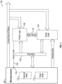
- the computer system 100 includes a microprocessor 102, a parity RAM 104, a Parity Logic component (Parity Logic 106) and a data bus 108.
- the Parity Logic 106 includes a piece of hardware that performs the calculation and comparison of the parity bits to detect RAM parity error.
- the microprocessor 102 includes a flash ROM 110 and an internal RAM 112.
- the flash ROM 110 holds non-volatile instructions and data, such as software code for a RAM test, RAM parity error detection and handling, and a RAM parity error handling lookup table.
- the internal RAM 112 holds temporary data. To simplify the processing performed using the methods disclosed herein, memory used for variables specifically created for RAM testing and RAM parity detection and handling as well as stack memory are allocated in the internal RAM. Use of the internal RAM provides better protection than parity RAM.
- the microprocessor 102 reads/writes data from/to the parity RAM 104 through the data bus 108.
- the data bus 108 provides a data communication path to the microprocessor 102, the parity RAM 104 and the Parity Logic 106.
- the Parity RAM 104 has Data Input/Output pins (D i/o ) and Parity Input/Output pins (P i/o ).
- the parity Input/Output pins are associated with the data Input/Output pins. Commonly, a P i/o is associated with eight D i/o .
- a single P i/o is associated with the 8 D i/o
- two P i/o are used, as follows: the first parity I/O pin P 0i/o is associated with the first group of 8 data I/O pins (i.e., from D 0i/o to D 7i/o ) and a second parity I/O pin P 1i/o is associated with a second group of 8 data I/O pins (i.e., from D 8i/o to D 15i/o ).
- parity RAM with 32 D i/o , 4 P i/o are used, as follows: the first parity pin P 0i/o is associated with the first group of 8 data I/O (i.e., from D 0i/o to D 7i/o ), the second parity pin P 1i/o is associated with the second group of 8 data I/O (i.e., from D 8i/o to D 15i/o ,), the third parity pin P 2i/o is associated with the third group of 8 data I/O (i.e., from D 16i/o to D 23i/o ), and a fourth parity pin P 3i/o is associated with a fourth group of 8 data I/O (from D 24i/o to D 31i/o ). Parity RAM with high numbers of data I/O pins have corresponding parity I/O pins following this same pattern.
- a parity bus 114 runs between the parity RAM 104 and the Parity Logic 106.
- Parity Logic 106 is used to calculate and set parity bits on the parity bus 114 based on data bits from the data bus 108, or to verify parity bits received from Parity RAM 104 via the parity bus 114.
- Parity Logic 106 calculates parity bits based on data bits from the data bus 108 and outputs the calculated parity bits to the parity bus 114.
- the parity bits on the parity bus 114 are written into the parity RAM 104 along with their corresponding data bits on the data bus 108.
- the parity RAM 104 outputs data bits to the data bus 108 and parity bits to the parity bus 114.
- Parity Logic 106 calculates parity bits based on the data bits on the data bus 108 and compares the calculated parity bits with their corresponding parity bits on the parity bus 114.
- a Parity Fault line 116 can be connected from Parity Logic 106 to an interrupt input pin 118 of the microprocessor 102. An interrupt can occur if a parity comparison fails while reading the parity RAM 104. In such instances, the Parity Fault line 116 is asserted by the Parity Logic 106, which triggers the interrupt at the microprocessor 102.
- FIG. 2 shows a flowchart 200 of a RAM test process with "RAM_ParityErrorFilter” module, in an embodiment.
- the RAM test provides an environment for the method of RAM parity error detection/handling disclosed herein.
- TEST_DATA1 and TEST_DATA2 are used for the RAM test. Examples of rules to set TEST_DATA1 value and TEST_DATA2 value are detailed here.
- TEST_DATA1 is equal to binary 01010101 (or 0x55 in hexadecimal notation) and TEST_DATA 2 is equal to binary 10101010 (or 0xAA in hexadecimal notation.
- the sizes of TEST_DATA1 and TEST_DATA2 can be set according to the size of the RAM test (0x5555 and 0xAAAA, respectively, for a 16-bit RAM test, 0x55555555 and 0xAAAAAAAA, respectively, for a 32-bit RAM test, etc.)
- cache and interrupts are disabled to ensure that the test is performed on RAM instead of on cache and to ensure that control does not switch to the interrupt handler in the middle of the RAM test while the RAM cell under test may be filled with a test value.
- the RAM test begins in box 202 when the RAM Test process is called.
- a local variable test status is initialized and is set to an initial value TEST_SUCCESS(0) and a local variable current address is set equal to Start_Address.
- a test is run to determine whether to continue the RAM test or to end the RAM test. If the current_adresss is greater than the End_Address or if test status is equal to TEST_FAIL(1), the method proceeds to box 208 in which the RAM test is ended and a test status is returned. Returning to box 206, if current address is less than or equal to the End_Address and test status is not equal to TEST_FAIL(1), the method proceeds to box 210.
- a RAM parity filter process is performed (i.e., a call is made to a RAM parity filter process, which is discussed in detail with respect to FIG. 3 ).
- TEST_DATA1 (e.g., 0x55555555 for a 32-bit RAM test) is written into the RAM cell at current address.
- the content value of the RAM cell at current address is read and checked against TEST_DATA1. If the value is not equal to TEST_DATA1, the method proceeds to box 220.
- test status is set to TEST_FAIL(1) and the content of a passed out parameter Fail_Address is set equal to current_addresss. From box 220, the method proceeds to box 226.
- TEST_DATA2 (e.g., 0xAAAAAAAA for a 32-bit RAM test) is written into the RAM cell at current address.
- TEST_DATA2 e.g., 0xAAAAAAAA for a 32-bit RAM test
- the content value of the RAM cell at current address is read and checked against TEST_DATA2. If the value is not equal to TEST_DATA2, the method proceeds to box 220. Otherwise, the method proceeds to box 226.
- hold_data is written back into the RAM cell at current address to restore its original value.
- the current address is then incremented to the next RAM cell address.
- the cache and interrupts are enabled. From box 228, the method returns to box 206.
- FIG. 3 shows a flowchart 300 of a RAM parity filter process. This process is called at box 214 of flowchart 200 ( FIG. 2 ). Since the filter is being run while interrupts are disabled, control does not go to the RAM parity error interrupt handler if a RAM parity error occurs.
- a RAM parity error interrupt status bit i.e., the bit corresponding to the RAM parity error event in the microprocessor interrupt status register
- the RAM parity error interrupt status bit is not set (i.e., read 0) and the process ends.
- the RAM parity error interrupt status bit is set to 1 and the filter checks each 8-bit data byte and its paired parity bit in the RAM cell and handles parity errors if present. In case of a parity error, the process ends when all the data bytes and parity bits in the RAM cell have been checked, the parity errors in the cell have been handled, and the content of the cell under test is read and saved to hold data.
- the RAM parity filter process begins at box 302.
- box 304 a check is performed on a RAM parity error interrupt status bit. If the RAM parity error interrupt status bit is not set, the method proceeds to box 306 in which the RAM parity filter procedure ends. Returning to box 304, if the RAM parity error interrupt status bit is set, the method proceeds to box 308.
- a local variable byteindex is set equal to 0.
- the byteIndex is compared to a value RAM_CELL_SIZE_IN_BYTE.
- RAM_CELL_SIZE_IN_BYTE specifies the number of data bytes in a RAM cell under test. It may be set to 1 for an 8-bit RAM test, to 2 for a 16-bit RAM test, to 4 for a 32-bit RAM test, or to 8 for a 64-bit RAM test. If byteindex is equal to or greater than RAM_CELL_SIZE_IN_BYTE, the method proceeds to box 312. In box 312, the contents of current address are read and saved to hold data. The method then proceeds to box 306 where the RAM parity filter method ends.
- the method proceeds to box 314.
- the RAM parity interrupt status bit is cleared (i.e., set to 0).
- a byte whose index is byteindex to the content of the RAM cell at the current address is read, and the byte is stored in local variable tempByte.
- a check is performed on the RAM parity error interrupt status bit. If the RAM parity error interrupt status bit is not set (i.e., read 0), the method proceeds to box 322. In box 322, the byteindex is incremented by 1. Returning to box 318, if the RAM parity error interrupt status bit is set, the method proceeds to box 320.
- box 320 a call is made to a RAM Parity Error Handler process, the contents of which are described with respect to FIG. 5 . From box 320, the method proceeds to box 322, in which the byteindex is incremented by 1. From box 320, the method returns to box 310.
- FIG. 4 is an example of a lookup table 400 that can be used by the RAM Parity Error Handler process of FIG. 5 .
- the RAM Parity Error Handler process searches the lookup table 400 to find an entry whose data field includes a faulty byte (i.e., a byte with a parity error) and to handle the parity error based on a parity error handler type found in the lookup table.
- the lookup table 400 can include multiple RAM parity error handler types. It is understood the lookup table 400 is only an illustrative example. The selection of each RAM parity error handler type in the lookup table depends on how the data field in Parity RAM is used in the application.
- the lookup table can have any size, any number of RAM parity error handler types.
- the RAM parity error handler types may be collectively defined in the following enumeration data structure in C programming language.
- SpecializedParityErrorHandler is a pointer pointing to a specialized parity error handler.
- Parameter errorPtr is a passed-in pointer, the address of the faulty byte.
- Parameter dataPtr is a passed-in pointer, the address of the data field impacted by the faulty byte.
- Parameter size is the size of the impacted data field.
- Data structure HDL_TYPE and RAM_ParityErrorHdlStruct are used to build the lookup table 400 for the simulation test.
- the lookup table 400 includes columns for data address or location 402, a size of the data field 404, a RAM parity error handler type 406, a default value 408, an address of a tied variable 410 and a specialized parity error handler 412.
- the data address may be denoted by &(data field name) and its size by sizeof(data field name), as shown in the first column (location 402) and the second column (size of the data field 404) of the lookup table 400.
- NULL(0, meaning Not Apply), PNULL(0, meaning Not Apply) are used to fill most of fields DefaultValue, *TiedVariable and *SpecializedParityErrorHandler() that are not accessed by the RAM parity error handling procedures.
- the first entry or row in the lookup table 400 is an entry for a merged data block used for a lab test and is inactive during normal operation.
- the RAM parity error handler type e.g, REFRESH_FAULT_BYTE
- REFRESH_FAULT_BYTE REFRESH_FAULT_BYTE
- the second entry or row is another merged data block, left for the default RAM parity error handler in the simulation test.
- the third entry or row is for variable SS8_1, and it is overwritten with default value 0x12 if it contains a byte with parity error.
- the fourth entry or row is for variable SS8_2, and it is overwritten with variable SS8_1 if it contains a byte with parity error.
- the fifth and sixth entries are more examples for overwrite with default value and overwrite with a tied variable, respectively.
- the seventh entry (RequestCfifo1) and eighth entry (RequestCfifo2) are for circular FIFO, whose parity error is handled by a specialized handler (e.g., CfifoRamParityErrorHandler()).
- the ninth entry is for a ProtectedQueue whose parity error is handled by simply refreshing the faulty byte.
- the tenth entry is for ST_State, whose parity error is handled by reinitializing the ST state machine.
- the last entry is for FD_Block, another instance left for the default RAM parity error handler in the simulation test.
- the lookup table 400 can be created by obtaining the data field name and address (column 1) from a software build map file.
- the data fields are normally sorted as per their memory addresses in the map file. If not sorted in the map file, they can be easily sorted using their numeric addresses from the map file before being used to populate the lookup table.
- a binary search method may be used to speed up the searching of the sorted lookup table.
- the lookup table can be assembled so with the start address and data block size for an entry in the lookup table with parity error handler type REFRESH FAULTY BYTE or FALLBACK_TO_DEFAULT_HANDLER. Doing so reduces the number of entries in the lookup table and allows for a catch-all of names and sizes of the data fields in the data block.
- FIG. 5 shows a flowchart 500 for the RAM parity error handler process, in an embodiment.
- a RAM parity error is handled depends on the application for which the RAM byte is being used. For instance, a data variable with a faulty byte (short for byte with parity error in this disclosure) may be corrected using its tied data variable because it is periodically set by the tied data variable or is used to set the tied data variable. In another instance, a data variable with a faulty byte may be corrected and set to its default safe value, which is a similar technique used to set a corrupted parameter received in a communication system.
- the RAM parity error handler may refresh the faulty byte (i.e., read the faulty byte and write the read value back to the faulty byte in RAM) to get rid of the parity error and let a built-in error correction correct the faulty byte later.
- the RAM parity error handler may also refresh the faulty byte in an inactive RAM block, such as the RAM blocks used for certain tests that are inactive, and data in the RAM block is never used at the operation.
- Specialized RAM parity error handlings may be used for some parity RAM applications. For instance, when a parity error occurs in a CFIFO (Circular-buffer-based FIFO) control field, it may make sense to reinitialize the CFIFO. When a parity error occurs in a CFIFO enqueued record, it may make sense to remove the faulty record from the CFIFO enqueued record list and set 0 to the faulty byte to clear the parity error with the faulty byte. When a parity error occurs in a CFIFO free record, the faulty byte may be set to 0 to clear the parity error with the faulty byte. For another instance of specialized RAM parity error handlings, when a parity error occurs in a critical data field of a component, it may make sense to reinitialize the component for the error recovery without restarting the system.
- CFIFO Cirrcular-buffer-based FIFO
- a data variable with a faulty byte may be correct using a FALLBACK_TO_DEFAULT_HANDLER.
- This type allows flexibility and extensibility of RAM parity error handling.
- a software release may include accurate RAM parity error handlings (overwrite with default value, overwrite with tied variable, refresh faulty byte and specialized handler types) for certain data fields and/or parity RAM blocks and leave the rest for the default RAM parity error handler, and future software releases may include accurate RAM parity error handlings for more data fields and/or parity RAM blocks.
- the RAM parity error handler process begins at box 502 in FIG. 5 .
- the lookup table 400 is searched for an entry that has the faulty byte with the parity error based on the address of the faulty byte.
- a decision is made based on whether the entry is found in the lookup table. If no entry is found, the method proceeds to box 508.
- the faulty byte is overwritten with 0.
- the RAM parity error interrupt register status bit is cleared, and the parity error may be logged if desired. From box 510, the method proceeds to box 542 where the RAM parity error handler procedure ends.
- box 512 a check is made whether the RAM Parity Error Handler type is OVERWRITE_WITH_DEFAULT_VALUE. If the Parity Error Handler type is OVERWRITE WITH DEFAULT VALUE, the method proceeds to box 514. In box 514, the impacted data field is overwritten with its default value. (For example, in the third entry of lookup table 400, the Parity Error Handler type is equal to OVERWRITE WITH DEFAULT VALUE, and the default value is 0x12.) In box 516, the RAM Parity Error Interrupt Status bit is cleared the parity error may be logged. From box 516, the method proceeds to box 542 where the RAM parity error handler process ends.
- the method proceeds to box 518.
- a check is made on the Parity Error Handler Type. If the Parity Error Handler Type is equal to OVERWRITE WITH_TIED_VARIABLE, the method proceeds to box 520. In box 520, the impacted data field is overwritten with its tied variable.
- the Parity Error Handler type is equal to OVERWRITE WITH_TIED_VARIABLE, and the tied variable is SS8_1.
- the RAM Parity Error Interrupt Status bit is cleared, and the parity error may be logged. From box 522, the method proceeds to box 542 where the RAM parity error handler process ends.
- the method proceeds to box 524.
- a check is made on whether the Parity Error Handler Type is equal to REFRESH FAULTY BYTE. If the Parity Error Handler Type is equal to REFRESH_FAULTY_BYTE, the method proceeds to box 526. In box 526, the faulty byte is read and written back to correct the parity bit.
- the RAM Parity Error Handler type is equal to REFRESH_FAULTY_BYTE.
- the RAM Parity Error Interrupt Status bit is cleared, and the parity error may be logged. From box 528, the method proceeds to box 542 where the RAM parity error handler process ends.
- Parity Error Handler Type is not equal to REFRESH_FAULTY_BYTE, the method proceeds to box 530.
- a check is made on whether the Parity Error Handler Type is equal to SPECIALIZED_HANDLER. If the Parity Error Handler Type is equal to SPECIALIZED_HANDLER, the method proceeds to box 532.
- a call is made to a Specialized RAM Parity Error Handler process. Note the RAM parity error is fixed, the error logged, and the RAM parity error interrupt status bit cleared in the specialized RAM parity error handler. From box 532, the method proceeds to box 542 where the RAM parity error handler process ends.
- Parity Error Handler Type is not equal to SPECIALIZED_HANDLER, the method proceeds to box 534.
- box 534 a check is made on whether the Parity Error Handler Type is equal to FALLBACK_TO DEFAULT _HANDLER. If the Parity Error Handler Type is equal to FALLBACK TO DEFAULT HANDLER, the method proceeds to box 536. In box 536, the parity error may be logged. From box 536, the method proceeds to box 542 where the process ends. In this case, the RAM parity error handling falls back to the default RAM parity error handler, and the RAM parity error will be handled there.
- the method proceeds to box 540.
- Box 540 is reserved for possibly additional RAM parity error handler types to be added in the future. From box 534, the method proceeds to box 542 where the process ends.
- FIG. 6 shows a flowchart 600 of a RAM Parity Error Interrupt Handler procedure (It is also referred to herein as the default RAM parity error handler), in an embodiment.
- the RAM Parity Error Interrupt Handler procedure begins at box 602 when it is called.
- the method disclosed herein runs in the context of a RAM test, detecting and handling RAM parity errors that occur in a RAM cell under test.
- the method runs only when there is a parity error with a RAM cell under test. Therefore, the method does not interfere with the RAM test in cases where there are no parity errors in the RAM cell under test.
Landscapes
- Engineering & Computer Science (AREA)
- Theoretical Computer Science (AREA)
- Quality & Reliability (AREA)
- Physics & Mathematics (AREA)
- General Engineering & Computer Science (AREA)
- General Physics & Mathematics (AREA)
- Techniques For Improving Reliability Of Storages (AREA)
Abstract
Description
- Embodiments of the present disclosure are related to RAM operations in computer systems and, more particular, to a system and method for detecting and handling RAM parity errors in the context of a RAM test.
- A computer system may include a parity RAM that stores data bits, as well as parity bits which can be used to detect errors in data. Conventionally, RAM parity errors are handled using an RAM parity error interrupt handler routine implemented in a microprocessor. A parity fault line is connected to an interrupt input pin of the microprocessor. When a parity error occurs while reading the parity RAM, the parity fault line is asserted (i.e., a signal is sent over the parity fault line), which triggers a RAM parity interrupt at the microprocessor. The RAM parity error interrupt handler handles the parity error by either restarting the system or by halting the system, both of which result in a disruption of services. There is therefore a need to handle parity bit errors without having to restart/halt the computer system.
- According to an embodiment, a method of detecting and handling a RAM parity error is disclosed. The method includes creating a lookup table with a plurality of entries, each entry including a data location and a RAM parity error handler type, obtaining an address of a faulty byte detected during a RAM test on the parity RAM, searching the lookup table for an entry that matches the faulty byte based on the address of the faulty byte, obtaining the RAM parity error handler type from the entry, and fixing a data field impacted by the faulty byte based on the RAM parity error handler type.
- In addition to one or more of the features described above, wherein each entry further includes a RAM parity error handler associated with the RAM parity error handler type, the method further comprises obtaining the RAM parity error handler corresponding to the RAM parity error handler type and fixing the data field impacted by the faulty byte using the RAM parity error handler.
- In addition to one or more of the features described above, the RAM parity error handler includes at least one of: (i) a default value; (ii) a tied variable; (iii) a faulty byte refresh; and (iv) a specialized RAM parity error handler.
- In addition to one or more of the features described above, wherein the entry includes a size of a data field, the method further comprises searching the lookup table for the entry that matches the faulty byte based on the address of the faulty byte, the address and the size of the data field in the lookup table.
- In addition to one or more of the features described above, the RAM parity error handler type in an entry of the lookup table is determined by a developer of the RAM parity error handler and is based on an application for which a data field in the entry is used.
- In addition to one or more of the features described above, fixing the data field impacted by the faulty byte further comprises one of: (i) overwriting the faulty byte with a default value; (ii) overwriting the faulty byte with a tied variable; (iii) refreshing the faulty byte with a value read from the faulty byte; (iv) calling a specialized RAM parity error handler; and (v) use of a default RAM parity error handler.
- In addition to one or more of the features described above, the RAM parity error handler type is one of: (i) OVERWRITE_WITH DEFAULT_VALUE; (ii) OVERWRITE_WITH_TIED_VARIABLE; (iii) REFRESH_FAULTY_BYTE; (iv) SPECIALIZED HANDLER; and (v) FALLBACK_TO DEFAULT HANDLER.
- In addition to one or more of the features described above, the method further includes writing 0 to the faulty byte when the faulty byte is not found in the lookup table. The faulty byte is a padding byte between the data fields in this case.
- According to another embodiment, a computer system is disclosed. The computer system includes a memory storing therein a lookup table, the lookup table having a plurality of entries, each entry including a data location and a RAM parity error handler type, and a processor configured to obtain an address of a faulty byte detected during a RAM test on the parity RAM, search the lookup table for an entry that contains the faulty byte based on the address of the faulty byte, obtain the RAM parity error handler type from the entry, and fix a data field impacted by the faulty byte based on the RAM parity error handler type.
- In addition to one or more of the features described above, wherein each entry further includes a parity handler associated with the RAM parity error handler type, the processor is further configured to obtain the RAM parity error handler corresponding to the RAM parity error handler type and fix the data field impacted by the faulty byte using the RAM parity error handler.
- In addition to one or more of the features described above, the RAM parity error handler includes at least one of: (i) a default value; (ii) a tied variable; (iii) a faulty byte refresh; and (iv) a specialized RAM parity error handler.
- In addition to one or more of the features described above, the RAM parity error handler type in the lookup table is determined by a developer of the RAM parity error handler and is based on an application for which a data field in the entry is used.
- In addition to one or more of the features described above, the processor is further configured to fix the data field impacted by the faulty byte by performing one of (i) overwriting the faulty byte with a default value; (ii) overwriting the faulty byte with a tied variable; (iii) refreshing the faulty byte with a value read from the faulty byte; (iv) calling a specialized RAM parity error handler; and (v) use of a default RAM parity error handler.
- In addition to one or more of the features described above, the RAM parity error handler type includes at least one of: (i) OVERWRITE_WITH DEFAULT_VALUE; (ii) OVERWRITE WITH_TIED_VARIABLE; (iii) REFRESH_FAULTY_BYTE; (iv) SPECIALIZED_HANDLER; and (v) FALLBACK_TO DEFAULT HANDLER.
- In addition to one or more of the features described above, the processor is further configured to write 0 to the faulty byte when the faulty byte is not found in the lookup table. The faulty byte is a padding byte between the data fields in this case.
- The following descriptions should not be considered limiting in any way. With reference to the accompanying drawings, like elements are numbered alike:
-
FIG. 1 shows a block diagram of a computer system in an illustrative embodiment; -
FIG. 2 shows a flowchart of a RAM test process with a "RAM_ParityErrorFilter" module, in an embodiment. -
FIG. 3 shows a flowchart of a RAM parity filter process; -
FIG. 4 is an example of a lookup table that can be used by the RAM Parity Error Handling process; -
FIG. 5 shows a flowchart for the RAM parity error handler process, in an embodiment; and -
FIG. 6 shows a flowchart of a RAM Parity Error Interrupt Handler procedure used as a RAM parity error default handler in this disclosure, in an embodiment. - A detailed description of one or more embodiments of the disclosed apparatus and method are presented herein by way of exemplification and not limitation with reference to the Figures.
- With reference now to
FIG. 1 , a block diagram of acomputer system 100 is shown in an illustrative embodiment. For ease of illustration, the block diagram only shows major components working with parity RAM and RAM parity handling. Thecomputer system 100 includes amicroprocessor 102, aparity RAM 104, a Parity Logic component (Parity Logic 106) and adata bus 108. The Parity Logic 106 includes a piece of hardware that performs the calculation and comparison of the parity bits to detect RAM parity error. Themicroprocessor 102 includes aflash ROM 110 and aninternal RAM 112. Theflash ROM 110 holds non-volatile instructions and data, such as software code for a RAM test, RAM parity error detection and handling, and a RAM parity error handling lookup table. Theinternal RAM 112 holds temporary data. To simplify the processing performed using the methods disclosed herein, memory used for variables specifically created for RAM testing and RAM parity detection and handling as well as stack memory are allocated in the internal RAM. Use of the internal RAM provides better protection than parity RAM. Themicroprocessor 102 reads/writes data from/to theparity RAM 104 through thedata bus 108. Thedata bus 108 provides a data communication path to themicroprocessor 102, theparity RAM 104 and the ParityLogic 106. - The
Parity RAM 104 has Data Input/Output pins (Di/o) and Parity Input/Output pins (Pi/o). The parity Input/Output pins are associated with the data Input/Output pins. Commonly, a Pi/o is associated with eight Di/o. For example, for a parity RAM with 8 Di/o, a single Pi/o is associated with the 8 Di/o For a parity RAM with 16 Di/o, two Pi/o are used, as follows: the first parity I/O pin P0i/o is associated with the first group of 8 data I/O pins (i.e., from D0i/o to D7i/o) and a second parity I/O pin P1i/o is associated with a second group of 8 data I/O pins (i.e., from D8i/o to D15i/o). For a parity RAM with 32 Di/o, 4 Pi/o are used, as follows: the first parity pin P0i/o is associated with the first group of 8 data I/O (i.e., from D0i/o to D7i/o), the second parity pin P1i/o is associated with the second group of 8 data I/O (i.e., from D8i/o to D15i/o,), the third parity pin P2i/o is associated with the third group of 8 data I/O (i.e., from D16i/o to D23i/o), and a fourth parity pin P3i/o is associated with a fourth group of 8 data I/O (from D24i/o to D31i/o). Parity RAM with high numbers of data I/O pins have corresponding parity I/O pins following this same pattern. - A
parity bus 114 runs between theparity RAM 104 and the Parity Logic 106. Parity Logic 106 is used to calculate and set parity bits on theparity bus 114 based on data bits from thedata bus 108, or to verify parity bits received from ParityRAM 104 via theparity bus 114. - For a write procedure at
parity RAM 104,Parity Logic 106 calculates parity bits based on data bits from thedata bus 108 and outputs the calculated parity bits to theparity bus 114. The parity bits on theparity bus 114 are written into theparity RAM 104 along with their corresponding data bits on thedata bus 108. For a read procedure at theparity RAM 104, theparity RAM 104 outputs data bits to thedata bus 108 and parity bits to theparity bus 114. ParityLogic 106 calculates parity bits based on the data bits on thedata bus 108 and compares the calculated parity bits with their corresponding parity bits on theparity bus 114. - A Parity
Fault line 116 can be connected from Parity Logic 106 to aninterrupt input pin 118 of themicroprocessor 102. An interrupt can occur if a parity comparison fails while reading theparity RAM 104. In such instances, the Parity Faultline 116 is asserted by the ParityLogic 106, which triggers the interrupt at themicroprocessor 102. -
FIG. 2 shows aflowchart 200 of a RAM test process with "RAM_ParityErrorFilter" module, in an embodiment. As shown inFIG. 2 , the RAM test provides an environment for the method of RAM parity error detection/handling disclosed herein. - Test data patterns TEST_DATA1 and TEST_DATA2 are used for the RAM test. Examples of rules to set TEST_DATA1 value and TEST_DATA2 value are detailed here. For an 8-bit RAM test, TEST_DATA1 is equal to binary 01010101 (or 0x55 in hexadecimal notation) and TEST_DATA 2 is equal to binary 10101010 (or 0xAA in hexadecimal notation. The sizes of TEST_DATA1 and TEST_DATA2 can be set according to the size of the RAM test (0x5555 and 0xAAAA, respectively, for a 16-bit RAM test, 0x55555555 and 0xAAAAAAAA, respectively, for a 32-bit RAM test, etc.)
- During the RAM test process, cache and interrupts are disabled to ensure that the test is performed on RAM instead of on cache and to ensure that control does not switch to the interrupt handler in the middle of the RAM test while the RAM cell under test may be filled with a test value.
- The RAM test begins in
box 202 when the RAM Test process is called. Inbox 204, a local variable test status is initialized and is set to an initial value TEST_SUCCESS(0) and a local variable current address is set equal to Start_Address. Inbox 206, a test is run to determine whether to continue the RAM test or to end the RAM test. If the current_adresss is greater than the End_Address or if test status is equal to TEST_FAIL(1), the method proceeds tobox 208 in which the RAM test is ended and a test status is returned. Returning tobox 206, if current address is less than or equal to the End_Address and test status is not equal to TEST_FAIL(1), the method proceeds tobox 210. - In
box 210, cache and interrupts are disabled. Inbox 212, the content of the RAM cell at current address is read and saved to a local variable hold data for temporary storage. Inbox 214, a RAM parity filter process is performed (i.e., a call is made to a RAM parity filter process, which is discussed in detail with respect toFIG. 3 ). - In
box 216, TEST_DATA1 (e.g., 0x55555555 for a 32-bit RAM test) is written into the RAM cell at current address. Inbox 218, the content value of the RAM cell at current address is read and checked against TEST_DATA1. If the value is not equal to TEST_DATA1, the method proceeds tobox 220. Inbox 220, test status is set to TEST_FAIL(1) and the content of a passed out parameter Fail_Address is set equal to current_addresss. Frombox 220, the method proceeds tobox 226. - Returning to
box 218 if the value read from the RAM cell at current address is equal to TEST_DATA1, the method proceeds tobox 222. Inbox 222, TEST_DATA2 (e.g., 0xAAAAAAAA for a 32-bit RAM test) is written into the RAM cell at current address. Inbox 224, the content value of the RAM cell at current address is read and checked against TEST_DATA2. If the value is not equal to TEST_DATA2, the method proceeds tobox 220. Otherwise, the method proceeds tobox 226. - In
box 226, hold_data is written back into the RAM cell at current address to restore its original value. The current address is then incremented to the next RAM cell address. Inbox 228, the cache and interrupts are enabled. Frombox 228, the method returns tobox 206. -
FIG. 3 shows aflowchart 300 of a RAM parity filter process. This process is called atbox 214 of flowchart 200 (FIG. 2 ). Since the filter is being run while interrupts are disabled, control does not go to the RAM parity error interrupt handler if a RAM parity error occurs. When theParity Fault line 116 is asserted (after a RAM cell with parity error is read), a RAM parity error interrupt status bit (i.e., the bit corresponding to the RAM parity error event in the microprocessor interrupt status register) is set to 1. If no RAM parity error is present in the RAM cell under test, the RAM parity error interrupt status bit is not set (i.e., read 0) and the process ends. If the RAM cell contains a parity error, the RAM parity error interrupt status bit is set to 1 and the filter checks each 8-bit data byte and its paired parity bit in the RAM cell and handles parity errors if present. In case of a parity error, the process ends when all the data bytes and parity bits in the RAM cell have been checked, the parity errors in the cell have been handled, and the content of the cell under test is read and saved to hold data. - The RAM parity filter process begins at
box 302. Inbox 304, a check is performed on a RAM parity error interrupt status bit. If the RAM parity error interrupt status bit is not set, the method proceeds tobox 306 in which the RAM parity filter procedure ends. Returning tobox 304, if the RAM parity error interrupt status bit is set, the method proceeds tobox 308. - In
box 308, a local variable byteindex is set equal to 0. Inbox 310, the byteIndex is compared to a value RAM_CELL_SIZE_IN_BYTE. RAM_CELL_SIZE_IN_BYTE specifies the number of data bytes in a RAM cell under test. It may be set to 1 for an 8-bit RAM test, to 2 for a 16-bit RAM test, to 4 for a 32-bit RAM test, or to 8 for a 64-bit RAM test. If byteindex is equal to or greater than RAM_CELL_SIZE_IN_BYTE, the method proceeds tobox 312. Inbox 312, the contents of current address are read and saved to hold data. The method then proceeds tobox 306 where the RAM parity filter method ends. - Returning to
box 310, if byteindex is less than RAM_CELL SIZE IN BYTE, the method proceeds tobox 314. Inbox 314, the RAM parity interrupt status bit is cleared (i.e., set to 0). In box 316, a byte whose index is byteindex to the content of the RAM cell at the current address is read, and the byte is stored in local variable tempByte. Inbox 318, a check is performed on the RAM parity error interrupt status bit. If the RAM parity error interrupt status bit is not set (i.e., read 0), the method proceeds tobox 322. Inbox 322, the byteindex is incremented by 1. Returning tobox 318, if the RAM parity error interrupt status bit is set, the method proceeds tobox 320. - In
box 320, a call is made to a RAM Parity Error Handler process, the contents of which are described with respect toFIG. 5 . Frombox 320, the method proceeds tobox 322, in which the byteindex is incremented by 1. Frombox 320, the method returns tobox 310. -
FIG. 4 is an example of a lookup table 400 that can be used by the RAM Parity Error Handler process ofFIG. 5 . The RAM Parity Error Handler process searches the lookup table 400 to find an entry whose data field includes a faulty byte (i.e., a byte with a parity error) and to handle the parity error based on a parity error handler type found in the lookup table. The lookup table 400 can include multiple RAM parity error handler types. It is understood the lookup table 400 is only an illustrative example. The selection of each RAM parity error handler type in the lookup table depends on how the data field in Parity RAM is used in the application. The lookup table can have any size, any number of RAM parity error handler types. - In an embodiment, The RAM parity error handler types may be collectively defined in the following enumeration data structure in C programming language.
       typedef enum HDL_TPYE ENUM
       {
          OVERWRITE WITH DEFAULT_VALUE = 1,
          OVERWRITE WITH_TIED_VARIABLE,
          REFRESH FAULTY BYTE,
          SPECIALIZED_HANDLER,
          FALLBACK_TO DEFAULT HANDLER
       } HDL_TYPE;
A major data structure may be defined below in C programming language

Claims (15)
- A method of detecting and handling a RAM parity error, comprising:creating a lookup table with a plurality of entries, each entry including a data location and a RAM parity error handler type;obtaining an address of a faulty byte detected during a RAM test on the parity RAM;searching the lookup table for an entry that matches the faulty byte based on the address of the faulty byte;obtaining the RAM parity error handler type from the entry; andfixing a data field impacted by the faulty byte based on the RAM parity error handler type.
- The method of claim 1, wherein each entry further includes a RAM parity error handler associated with the RAM parity error handler type, further comprising obtaining the RAM parity error handler corresponding to the RAM parity error handler type and fixing the data field impacted by the faulty byte using the RAM parity error handler.
- The method of claim 2, wherein the RAM parity error handler includes at least one of: (i) a default value; (ii) a tied variable; (iii) a faulty byte refresh; and (iv) a specialized RAM parity error handler.
- The method of claim 1, 2 or 3, wherein the entry includes a size of a data field, further comprising searching the lookup table for the entry that matches the faulty byte based on the address of the faulty byte, the address and the size of the data field in the lookup table.
- The method of any preceding claim, wherein the RAM parity error handler type in an entry of the lookup table is determined by a developer of the RAM parity error handler and is based on an application for which a data field in the entry is used.
- The method of any preceding claim, wherein fixing the data field impacted by the faulty byte further comprises one of: (i) overwriting the faulty byte with a default value; (ii) overwriting the faulty byte with a tied variable; (iii) refreshing the faulty byte with a value read from the faulty byte; (iv) calling a specialized RAM parity error handler; and (v) use of a default RAM parity error handler.
- The method of any preceding claim, wherein the RAM parity error handler type is at of: (i) OVERWRITE_WITH_DEFAULT_VALUE; (ii) OVERWRITE WITH_TIED VARIABLE; (iii) REFRESH_FAULTY_BYTE; (iv) SPECIALIZED_HANDLER; and (v) FALLBACK_TO_DEFAULT_HANDLER.
- The method of any preceding claim, further comprising writing 0 to the faulty byte when the faulty byte is not found in the lookup table.
- A computer system, comprising:a memory storing therein a lookup table, the lookup table having a plurality of entries, each entry including a data location and a RAM parity error handler type;a processor configured to:obtain an address of a faulty byte detected during a RAM test on the parity RAM;search the lookup table for an entry that contains the faulty byte based on the address of the faulty byte;obtain the RAM parity error handler type from the entry; andfix a data field impacted by the faulty byte based on the RAM parity error handler type.
- The computer system of claim 9, wherein each entry further includes a parity handler associated with the RAM parity error handler type, and the processor is further configured to obtain the RAM parity error handler corresponding to the RAM parity error handler type and fix the data field impacted by the faulty byte using the RAM parity error handler.
- The computer system of claim 10, wherein the RAM parity error handler includes at least one of: (i) a default value; (ii) a tied variable; (iii) a faulty byte refresh; and (iv) a specialized RAM parity error handler.
- The computer system of claim 9, 10 or 11, wherein the RAM parity error handler type in the lookup table is determined by a developer of the RAM parity error handler and is based on an application for which a data field in the entry is used.
- The computer system of any of claims 9 to 12, wherein the processor is further configured to fix the data field impacted by the faulty byte by performing one of: (i) overwriting the faulty byte with a default value; (ii) overwriting the faulty byte with a tied variable; (iii) refreshing the faulty byte with a value read from the faulty byte; (iv) calling a specialized RAM parity error handler; and (v) use of a default RAM parity error handler.
- The computer system of any of claims 9 to 13, wherein the RAM parity error handler types includes at least one of (i) OVERWRITE_WITH DEFAULT_VALUE; (ii) OVERWRITE WITH_TIED_VARIABLE; (iii) REFRESH_FAULTY_BYTE; (iv) SPECIALIZED_HANDLER; and (v) FALLBACK_TO DEFAULT HANDLER.
- The computer system of any of claims 9 to 14, wherein the processor is further configured to write 0 to the faulty byte when the faulty byte is not found in the lookup table.
Applications Claiming Priority (1)
| Application Number | Priority Date | Filing Date | Title |
|---|---|---|---|
| US18/177,336 US12130700B2 (en) | 2023-03-02 | 2023-03-02 | RAM test with parity error detection and handling |
Publications (2)
| Publication Number | Publication Date |
|---|---|
| EP4425497A1 true EP4425497A1 (en) | 2024-09-04 |
| EP4425497B1 EP4425497B1 (en) | 2025-12-31 |
Family
ID=90054199
Family Applications (1)
| Application Number | Title | Priority Date | Filing Date |
|---|---|---|---|
| EP24159195.7A Active EP4425497B1 (en) | 2023-03-02 | 2024-02-22 | RAM testing with parity error detection and handling |
Country Status (2)
| Country | Link |
|---|---|
| US (1) | US12130700B2 (en) |
| EP (1) | EP4425497B1 (en) |
Citations (2)
| Publication number | Priority date | Publication date | Assignee | Title |
|---|---|---|---|---|
| US20200301776A1 (en) * | 2018-01-25 | 2020-09-24 | Samsung Electronics Co., Ltd. | Semiconductor memory devices, memory systems and methods of operating semiconductor memory devices |
| US20210265002A1 (en) * | 2020-02-26 | 2021-08-26 | Taiwan Semiconductor Manufacturing Co., Ltd. | Method and system for replacement of memory cells |
Family Cites Families (16)
| Publication number | Priority date | Publication date | Assignee | Title |
|---|---|---|---|---|
| IT1202527B (en) | 1987-02-12 | 1989-02-09 | Honeywell Inf Systems | MEMORY SYSTEM AND RELATED ERROR DETECTION-CORRECTION APPARATUS |
| WO1993004432A2 (en) | 1991-08-16 | 1993-03-04 | Multichip Technology | High-performance dynamic memory system |
| US6041426A (en) | 1995-04-07 | 2000-03-21 | National Semiconductor Corporation | Built in self test BIST for RAMS using a Johnson counter as a source of data |
| US6332181B1 (en) | 1998-05-04 | 2001-12-18 | International Business Machines Corporation | Recovery mechanism for L1 data cache parity errors |
| US7251755B2 (en) * | 2004-02-13 | 2007-07-31 | Intel Corporation | Apparatus and method for maintaining data integrity following parity error detection |
| US7594158B2 (en) | 2005-08-26 | 2009-09-22 | Hewlett-Packard Development Company, L.P. | Parity error checking and compare using shared logic circuitry in a ternary content addressable memory |
| US20120260138A1 (en) * | 2011-04-05 | 2012-10-11 | Downing Iii Robert L | Error logging in a storage device |
| US8467914B2 (en) | 2011-08-01 | 2013-06-18 | Hamilton Sunstrand Corporation | Bit transmission verification in an ARINC-based system |
| KR20130098039A (en) * | 2012-02-27 | 2013-09-04 | 삼성전자주식회사 | Semiconductor device capable of rescuing defective characteristics after packaging |
| US9223665B2 (en) * | 2013-03-15 | 2015-12-29 | Micron Technology, Inc. | Apparatuses and methods for memory testing and repair |
| CN105608027B (en) | 2015-12-18 | 2018-10-19 | 华为技术有限公司 | Non-volatile memory apparatus and the method for accessing non-volatile memory apparatus |
| IT201800003233A1 (en) * | 2018-03-02 | 2019-09-02 | Stmicroelectronics Application Gmbh | PROCESSING SYSTEM, RELATED INTEGRATED CIRCUIT AND PROCEDURE |
| US11145336B2 (en) * | 2019-10-30 | 2021-10-12 | Micron Technology, Inc. | Program pulse control using environmental parameters |
| WO2022028209A1 (en) * | 2020-08-05 | 2022-02-10 | 华为技术有限公司 | Memory failure processing method and apparatus |
| US12379991B2 (en) * | 2021-01-22 | 2025-08-05 | Micron Technology, Inc. | Error detection event mechanism |
| KR102922695B1 (en) * | 2021-04-15 | 2026-02-04 | 매그나칩 반도체 유한회사 | Apparatus and Method for repairing Static Random Access Memory |
-
2023
- 2023-03-02 US US18/177,336 patent/US12130700B2/en active Active
-
2024
- 2024-02-22 EP EP24159195.7A patent/EP4425497B1/en active Active
Patent Citations (2)
| Publication number | Priority date | Publication date | Assignee | Title |
|---|---|---|---|---|
| US20200301776A1 (en) * | 2018-01-25 | 2020-09-24 | Samsung Electronics Co., Ltd. | Semiconductor memory devices, memory systems and methods of operating semiconductor memory devices |
| US20210265002A1 (en) * | 2020-02-26 | 2021-08-26 | Taiwan Semiconductor Manufacturing Co., Ltd. | Method and system for replacement of memory cells |
Also Published As
| Publication number | Publication date |
|---|---|
| US12130700B2 (en) | 2024-10-29 |
| US20240296087A1 (en) | 2024-09-05 |
| EP4425497B1 (en) | 2025-12-31 |
Similar Documents
| Publication | Publication Date | Title |
|---|---|---|
| JP4617405B2 (en) | Electronic device for detecting defective memory, defective memory detecting method, and program therefor | |
| EP0227749B1 (en) | Fault tolerant data processing system and method therefor | |
| US8261140B2 (en) | Uninitialized memory detection using error correction codes and built-in self test | |
| US7117348B2 (en) | Method and system for detecting the validity of configuration data | |
| US4710866A (en) | Method and apparatus for validating prefetched instruction | |
| US4483003A (en) | Fast parity checking in cache tag memory | |
| JP2519286B2 (en) | Address line test method | |
| CN116382958B (en) | A memory error processing method and computing device | |
| EP0321793A2 (en) | Apparatus for forcing a reload from main memory upon cache memory error | |
| US4805095A (en) | Circuit and a method for the selection of original data from a register log containing original and modified data | |
| US20110320911A1 (en) | Computer System and Method of Protection for the System's Marking Store | |
| US5357521A (en) | Address sensitive memory testing | |
| US4368532A (en) | Memory checking method | |
| JPH04220744A (en) | Function testing method of cache tag ram in limited access processor system | |
| CN121646813A (en) | Systems and methods for testing error correction code (ECC) logic faults in automotive safety systems. | |
| US6539338B1 (en) | Self-diagnostic testing of a network interface adapter | |
| EP4425497B1 (en) | RAM testing with parity error detection and handling | |
| US6035436A (en) | Method and apparatus for fault on use data error handling | |
| US6799285B2 (en) | Self-checking multi-threaded processor | |
| US5996062A (en) | Method and apparatus for controlling an instruction pipeline in a data processing system | |
| US7596036B2 (en) | Memory control circuit, microcomputer, and data rewriting method | |
| GB2292470A (en) | Rom patching | |
| US20010052114A1 (en) | Data processing apparatus | |
| KR102389534B1 (en) | Back-up and restoration of register data | |
| US20070226471A1 (en) | Data processing apparatus |
Legal Events
| Date | Code | Title | Description |
|---|---|---|---|
| PUAI | Public reference made under article 153(3) epc to a published international application that has entered the european phase |
Free format text: ORIGINAL CODE: 0009012 |
|
| STAA | Information on the status of an ep patent application or granted ep patent |
Free format text: STATUS: THE APPLICATION HAS BEEN PUBLISHED |
|
| AK | Designated contracting states |
Kind code of ref document: A1 Designated state(s): AL AT BE BG CH CY CZ DE DK EE ES FI FR GB GR HR HU IE IS IT LI LT LU LV MC ME MK MT NL NO PL PT RO RS SE SI SK SM TR |
|
| STAA | Information on the status of an ep patent application or granted ep patent |
Free format text: STATUS: REQUEST FOR EXAMINATION WAS MADE |
|
| 17P | Request for examination filed |
Effective date: 20250303 |
|
| GRAP | Despatch of communication of intention to grant a patent |
Free format text: ORIGINAL CODE: EPIDOSNIGR1 |
|
| STAA | Information on the status of an ep patent application or granted ep patent |
Free format text: STATUS: GRANT OF PATENT IS INTENDED |
|
| RIC1 | Information provided on ipc code assigned before grant |
Ipc: G11C 29/42 20060101AFI20250728BHEP Ipc: G11C 29/00 20060101ALI20250728BHEP Ipc: G06F 11/07 20060101ALI20250728BHEP Ipc: G11C 29/52 20060101ALI20250728BHEP Ipc: G11C 29/04 20060101ALN20250728BHEP Ipc: G06F 11/10 20060101ALN20250728BHEP |
|
| INTG | Intention to grant announced |
Effective date: 20250811 |
|
| GRAS | Grant fee paid |
Free format text: ORIGINAL CODE: EPIDOSNIGR3 |
|
| GRAA | (expected) grant |
Free format text: ORIGINAL CODE: 0009210 |
|
| STAA | Information on the status of an ep patent application or granted ep patent |
Free format text: STATUS: THE PATENT HAS BEEN GRANTED |
|
| AK | Designated contracting states |
Kind code of ref document: B1 Designated state(s): AL AT BE BG CH CY CZ DE DK EE ES FI FR GB GR HR HU IE IS IT LI LT LU LV MC ME MK MT NL NO PL PT RO RS SE SI SK SM TR |
|
| REG | Reference to a national code |
Ref country code: CH Ref legal event code: F10 Free format text: ST27 STATUS EVENT CODE: U-0-0-F10-F00 (AS PROVIDED BY THE NATIONAL OFFICE) Effective date: 20251231 Ref country code: GB Ref legal event code: FG4D |
|
| REG | Reference to a national code |
Ref country code: DE Ref legal event code: R096 Ref document number: 602024001855 Country of ref document: DE |
|
| REG | Reference to a national code |
Ref country code: IE Ref legal event code: FG4D |
|
| REG | Reference to a national code |
Ref country code: LT Ref legal event code: MG9D |
|
| PG25 | Lapsed in a contracting state [announced via postgrant information from national office to epo] |
Ref country code: NO Free format text: LAPSE BECAUSE OF FAILURE TO SUBMIT A TRANSLATION OF THE DESCRIPTION OR TO PAY THE FEE WITHIN THE PRESCRIBED TIME-LIMIT Effective date: 20260331 |
|
| PG25 | Lapsed in a contracting state [announced via postgrant information from national office to epo] |
Ref country code: HR Free format text: LAPSE BECAUSE OF FAILURE TO SUBMIT A TRANSLATION OF THE DESCRIPTION OR TO PAY THE FEE WITHIN THE PRESCRIBED TIME-LIMIT Effective date: 20251231 Ref country code: FI Free format text: LAPSE BECAUSE OF FAILURE TO SUBMIT A TRANSLATION OF THE DESCRIPTION OR TO PAY THE FEE WITHIN THE PRESCRIBED TIME-LIMIT Effective date: 20251231 |
|
| PGFP | Annual fee paid to national office [announced via postgrant information from national office to epo] |
Ref country code: AT Payment date: 20260301 Year of fee payment: 3 |
|
| PG25 | Lapsed in a contracting state [announced via postgrant information from national office to epo] |
Ref country code: RS Free format text: LAPSE BECAUSE OF FAILURE TO SUBMIT A TRANSLATION OF THE DESCRIPTION OR TO PAY THE FEE WITHIN THE PRESCRIBED TIME-LIMIT Effective date: 20260331 |
|
| PGFP | Annual fee paid to national office [announced via postgrant information from national office to epo] |
Ref country code: FR Payment date: 20260121 Year of fee payment: 3 |
|
| PG25 | Lapsed in a contracting state [announced via postgrant information from national office to epo] |
Ref country code: LV Free format text: LAPSE BECAUSE OF FAILURE TO SUBMIT A TRANSLATION OF THE DESCRIPTION OR TO PAY THE FEE WITHIN THE PRESCRIBED TIME-LIMIT Effective date: 20251231 |
|
| PG25 | Lapsed in a contracting state [announced via postgrant information from national office to epo] |
Ref country code: BG Free format text: LAPSE BECAUSE OF FAILURE TO SUBMIT A TRANSLATION OF THE DESCRIPTION OR TO PAY THE FEE WITHIN THE PRESCRIBED TIME-LIMIT Effective date: 20251231 |
|
| REG | Reference to a national code |
Ref country code: NL Ref legal event code: MP Effective date: 20251231 |