EP4425189A1 - Capacitive mems device - Google Patents
Capacitive mems device Download PDFInfo
- Publication number
- EP4425189A1 EP4425189A1 EP23159362.5A EP23159362A EP4425189A1 EP 4425189 A1 EP4425189 A1 EP 4425189A1 EP 23159362 A EP23159362 A EP 23159362A EP 4425189 A1 EP4425189 A1 EP 4425189A1
- Authority
- EP
- European Patent Office
- Prior art keywords
- electrode
- static
- movable
- layer
- comb
- Prior art date
- Legal status (The legal status is an assumption and is not a legal conclusion. Google has not performed a legal analysis and makes no representation as to the accuracy of the status listed.)
- Pending
Links
Images


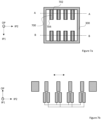

Classifications
-
- B—PERFORMING OPERATIONS; TRANSPORTING
- B81—MICROSTRUCTURAL TECHNOLOGY
- B81B—MICROSTRUCTURAL DEVICES OR SYSTEMS, e.g. MICROMECHANICAL DEVICES
- B81B3/00—Devices comprising flexible or deformable elements, e.g. comprising elastic tongues or membranes
- B81B3/0018—Structures acting upon the moving or flexible element for transforming energy into mechanical movement or vice versa, i.e. actuators, sensors, generators
- B81B3/0021—Transducers for transforming electrical into mechanical energy or vice versa
-
- G—PHYSICS
- G01—MEASURING; TESTING
- G01P—MEASURING LINEAR OR ANGULAR SPEED, ACCELERATION, DECELERATION, OR SHOCK; INDICATING PRESENCE, ABSENCE, OR DIRECTION, OF MOVEMENT
- G01P15/00—Measuring acceleration; Measuring deceleration; Measuring shock, i.e. sudden change of acceleration
- G01P15/02—Measuring acceleration; Measuring deceleration; Measuring shock, i.e. sudden change of acceleration by making use of inertia forces using solid seismic masses
- G01P15/08—Measuring acceleration; Measuring deceleration; Measuring shock, i.e. sudden change of acceleration by making use of inertia forces using solid seismic masses with conversion into electric or magnetic values
- G01P15/125—Measuring acceleration; Measuring deceleration; Measuring shock, i.e. sudden change of acceleration by making use of inertia forces using solid seismic masses with conversion into electric or magnetic values by capacitive pick-up
-
- B—PERFORMING OPERATIONS; TRANSPORTING
- B81—MICROSTRUCTURAL TECHNOLOGY
- B81B—MICROSTRUCTURAL DEVICES OR SYSTEMS, e.g. MICROMECHANICAL DEVICES
- B81B7/00—Microstructural systems ; Auxiliary parts of microstructural devices or systems
- B81B7/02—Microstructural systems ; Auxiliary parts of microstructural devices or systems containing distinct electrical or optical devices of particular relevance for their function, e.g. microelectro-mechanical systems [MEMS]
-
- B—PERFORMING OPERATIONS; TRANSPORTING
- B81—MICROSTRUCTURAL TECHNOLOGY
- B81C—PROCESSES OR APPARATUS SPECIALLY ADAPTED FOR THE MANUFACTURE OR TREATMENT OF MICROSTRUCTURAL DEVICES OR SYSTEMS
- B81C3/00—Assembling of devices or systems from individually processed components
- B81C3/002—Aligning microparts
-
- G—PHYSICS
- G01—MEASURING; TESTING
- G01P—MEASURING LINEAR OR ANGULAR SPEED, ACCELERATION, DECELERATION, OR SHOCK; INDICATING PRESENCE, ABSENCE, OR DIRECTION, OF MOVEMENT
- G01P15/00—Measuring acceleration; Measuring deceleration; Measuring shock, i.e. sudden change of acceleration
- G01P15/02—Measuring acceleration; Measuring deceleration; Measuring shock, i.e. sudden change of acceleration by making use of inertia forces using solid seismic masses
- G01P15/08—Measuring acceleration; Measuring deceleration; Measuring shock, i.e. sudden change of acceleration by making use of inertia forces using solid seismic masses with conversion into electric or magnetic values
- G01P15/0802—Details
-
- B—PERFORMING OPERATIONS; TRANSPORTING
- B81—MICROSTRUCTURAL TECHNOLOGY
- B81B—MICROSTRUCTURAL DEVICES OR SYSTEMS, e.g. MICROMECHANICAL DEVICES
- B81B2201/00—Specific applications of microelectromechanical systems
- B81B2201/02—Sensors
- B81B2201/0228—Inertial sensors
- B81B2201/0235—Accelerometers
-
- B—PERFORMING OPERATIONS; TRANSPORTING
- B81—MICROSTRUCTURAL TECHNOLOGY
- B81B—MICROSTRUCTURAL DEVICES OR SYSTEMS, e.g. MICROMECHANICAL DEVICES
- B81B2201/00—Specific applications of microelectromechanical systems
- B81B2201/03—Microengines and actuators
- B81B2201/033—Comb drives
-
- B—PERFORMING OPERATIONS; TRANSPORTING
- B81—MICROSTRUCTURAL TECHNOLOGY
- B81B—MICROSTRUCTURAL DEVICES OR SYSTEMS, e.g. MICROMECHANICAL DEVICES
- B81B2203/00—Basic microelectromechanical structures
- B81B2203/05—Type of movement
- B81B2203/051—Translation according to an axis parallel to the substrate
-
- B—PERFORMING OPERATIONS; TRANSPORTING
- B81—MICROSTRUCTURAL TECHNOLOGY
- B81C—PROCESSES OR APPARATUS SPECIALLY ADAPTED FOR THE MANUFACTURE OR TREATMENT OF MICROSTRUCTURAL DEVICES OR SYSTEMS
- B81C2203/00—Forming microstructural systems
- B81C2203/03—Bonding two components
- B81C2203/033—Thermal bonding
- B81C2203/036—Fusion bonding
-
- G—PHYSICS
- G01—MEASURING; TESTING
- G01P—MEASURING LINEAR OR ANGULAR SPEED, ACCELERATION, DECELERATION, OR SHOCK; INDICATING PRESENCE, ABSENCE, OR DIRECTION, OF MOVEMENT
- G01P15/00—Measuring acceleration; Measuring deceleration; Measuring shock, i.e. sudden change of acceleration
- G01P15/02—Measuring acceleration; Measuring deceleration; Measuring shock, i.e. sudden change of acceleration by making use of inertia forces using solid seismic masses
- G01P15/08—Measuring acceleration; Measuring deceleration; Measuring shock, i.e. sudden change of acceleration by making use of inertia forces using solid seismic masses with conversion into electric or magnetic values
- G01P2015/0862—Measuring acceleration; Measuring deceleration; Measuring shock, i.e. sudden change of acceleration by making use of inertia forces using solid seismic masses with conversion into electric or magnetic values being provided with particular means being integrated into a MEMS accelerometer structure for providing particular additional functionalities to those of a spring mass system
Definitions
- the present disclosure relates to microelectromechanical devices, and more particularly to microelectromechanical devices detecting or actuating motions capacitively in an in-plane direction.
- MEMS microelectromechanical system
- a MEMS includes mechanical or electromechanical elements, configured to implement a mechanical functionality in response to a detected phenomenon.
- a signal that corresponds with the detection may be generated by means of structural parts that are movable or structural parts that dynamically damp movement of parts that are movable in response to a detected phenomenon.
- Capacitance is widely used in MEMS to convert induced movements to electrical signals or to convert input voltage to induced motion.
- a conductive part that is movable and a static conductive part can be electrically isolated by an intermediate nonconductive part.
- the movable and static parts When the movable and static parts are connected into different potentials, they form a capacitive transducer, a capacitor.
- the static and movable conductive parts are typically arranged to have opposing planar surfaces and changes in capacitance relate to a change in overlapping area of the opposing surfaces, or a change in the distance between the opposing surfaces.
- FIG. 1a illustrates a sensing arrangement where capacitance of the parallel plate capacitor varies according to change in distance d between the plates.
- the shown capacitor includes a movable plate 100 and a static plate 102 that extend parallel to a plane along the two in-plane directions IP1 and IP2.
- the plates are separated by a distance d, and the movable plate 100 is able to move in the out-of-plane direction OP in response to a detected phenomenon so that the area A of overlap remains static, but the distance d-x varies with the change in displacement x.
- the capacitance change of this type of capacitor is not constant but varies with distance between the plates.
- the response can be approximately linear over a small range of displacements of the movable plate, but with larger motions, it is nonlinear.
- Figure 1b illustrates a sensing arrangement where capacitance of the parallel plate capacitor varies according to change in the area A of overlap between the plates.
- the movable plate 100 can move in the in-plane direction IP2 in response to a detected phenomenon so that the distance d between the plates remains static, the length I of the area of overlap remains static, but the width w+x of the area of overlap varies accordingly with the change in displacement x.
- the capacitance is directly proportional to the structural variable w.
- An object of the present disclosure is to describe a MEMS structure and a method for manufacturing the MEMS structure so as to address the above-described disadvantages.
- the disclosure is based on the idea of forming a static electrode and a movable electrode into a mechanical layer that includes a first and a second silicon layer.
- the gap between the static and movable electrodes for capacitive detection is arranged to the interface between the silicon layers, and their peripheries are closed by direct bonding to each other.
- the generated signal is arranged to vary according to overlap of the static and movable electrodes.
- the gap that separates static and movable electrodes is very accurately dimensioned, because it can be patterned into the interface between two directly bonded wafer layers.
- the accurate dimensioning enables accurate detection of overlap area of comb fingers over the gap, and use of area modulation enables linear signal response and large rotor motion.
- the schematic drawing of Figure 2 illustrates basic semiconducting layers of an example MEMS structure.
- the MEMS structure 200 includes a substrate layer 202 and a mechanical layer 204.
- the mechanical layer is patterned to include electromechanical elements applicable for implementing a mechanical function of the MEMS structure.
- the mechanical layer typically includes a cavity in which the electromechanical elements can move. The cavity may be enclosed between the substrate layer 202 and a further capping layer 220, and peripheral regions of the mechanical layer 204.
- the term layer refers here to a mainly planar thickness of a material.
- the substrate layer and the mechanical layer are wafer layers that may be formed of a single wafer, or two or more wafers bonded to each other.
- Wafer layers in MEMS structures may be patterned to include local recesses and/or protrusions, but due to their original wafer disc form, wafer layers include planar forms that in the total MEMS structure align to identifiable layer planes, each of which can be considered to be parallel to a reference device plane 206.
- the reference plane 206 extends into two mutually orthogonal in-plane directions IP1 and IP2.
- Figure 2 provides a side view to a section of the MEMS structure.
- the substrate layer 202 is described herein to be in the bottom of the MEMS structure so that a surface of each layer on the side of the substrate is called a bottom surface and a surface opposite it a top surface.
- the substrate layer 202 includes a bottom surface 210 facing outwards of the structure and a top surface 212 towards the next layer of the structure, and both surfaces are parallel to the reference plane 206.
- Surfaces of the layers may include local patterned sections, like cavities, recesses or protrusions, as shown with the mechanical layer 204 of Figure 2 , but in each layer, it is possible to identify planar forms that align to a plane that is parallel to the reference device plane 206.
- the substrate layer 202 and the mechanical layer 204 layer are electrically separated by an electrical insulator layer 208.
- Electrical separation means here that in parts where the substrate layer 202 and the mechanical layer 204 are in mechanical contact, the electrical insulator layer 208 is between them and electrically isolates one from another.
- the structure may include parts in which the mechanical layer has been etched off and there is thus no mechanical connection between the substrate layer 202 and the mechanical layer 204. In those parts, also the electrical insulator layer 208 may be removed from. In the example of Figure 2 , parts of the top surface 212 of the substrate layer 202 are not covered by the mechanical layer 204 and material of the electrical insulator layer 208 has been removed from those parts.
- the mechanical layer includes a first silicon layer 204-1 and a second silicon layer 204-2. At least parts of the first silicon layer 204-1 and the second silicon layer 204-2 are directly bonded to each other.
- Direct bonding also referred to as silicon direct bonding or silicon fusion bonding refers here to a wafer bonding process wherein two silicon wafers are bonded to each other without an added intermediate layer or elements.
- wafer surfaces may be pre-processed flat, clean and smooth so that when brought into contact, they stick together and form a weak bonding by physical forces. After this, adhesion based on intermolecular interactions including van der Waals forces, hydrogen bonds and strong covalent bonds may be increased by annealing.
- the type of created bonding is determined by the chemical species on the surfaces. In the case of silicon, hydrophilic and hydrophobic bonding is possible.
- the mechanical layer 204 is patterned to include at least one static electrode and at least one movable electrode.
- the static electrode and the movable electrode are capacitively connected to generate a signal that varies according to movement of the movable electrode in relation to the static electrode parallel to the device plane.
- static electrodes and movable electrodes of area modulated capacitors have been implemented in form of a device layer comb structures wherein comb fingers of static electrodes and movable electrodes are interdigitated in a same wafer layer and move parallel to the reference device plane so that the areas of overlap of the comb fingers correspond to overlap of their projections in the out-of-plane direction OP.
- static electrodes and movable electrodes of area modulated capacitors have in some alternative plans been formed into wafers interconnected through high temperature eutectic metal bonds controlled by oxide standoffs.
- an out-of-plane gap between static and movable electrodes extends in the out-of-plane direction OP and the areas of overlap area between static and movable electrodes corresponds to overlap of their projections to the reference device plane 206.
- the structure of Figure 2 shows a static electrode 214 and a movable electrode 216.
- the movable electrode 214 is in the first silicon layer 204-1 (the top part of the mechanical layer) and the static electrode 216 is in the second silicon layer 204-2 (the bottom part of the mechanical layer).
- the static electrode 214 and the movable electrode 216 are capacitively connected to generate a signal that varies according to movement of the movable electrode 216 in relation to the static electrode 214 parallel to the reference device plane. Provision of capacitive connection, for example, by electrically coupling the static electrode 214 to an external voltage source (not shown) is well known to a person skilled in the art.
- the signal varies according to movements of the movable electrode 216 in relation to the static electrode 214 in the second in-plane direction IP2.
- This variation corresponds to area of overlap of the movable electrode 216 and the static electrode 214 and can be determined from projections of the movable electrode 216 and the static electrode 214 into the reference device plane 206.
- the out-of-plane gap 218 between the static electrode 214 and the movable electrode 216 is a void space formed between the first silicon layer 204-1 and the second silicon layer 204-2.
- the out-of-plane gap is patterned inside the mechanical layer 204 before the first silicon layer 204-1 and the second silicon layer 204-2 are directly bonded to each other.
- bottom surface of the movable electrode 216 may be above a plane that is parallel to a bonding interface between bonded parts of the first silicon layer 204-1 and the second silicon layer 204-2.
- Figure 2 illustrates an example wherein the structure includes a plurality of static and movable comb fingers and bottom surfaces of the movable electrodes align to a plane that is parallel to the reference device plane 206 and above the bonding interface between the first silicon layer 204-1 and the second silicon layer 204-2.
- top surfaces of the movable electrodes align to a plane that is parallel to the reference device plane 206 and below the bonding interface between the first silicon layer 204-1 and the capping layer 220.
- Top surfaces of the static electrodes align to the bonding interface between the first silicon layer 204-1 and the second silicon layer 204-2.
- Bottom surfaces of the static electrodes are electrically insulated from the substrate layer by the electrical insulator layer 208.
- the second silicon layer may be patterned to include one or more anchors that are supported on the substrate layer though the electrical insulator layer 208 and dimensioned to provide a common point of support to the static electrodes.
- anchors may be released from the substrate layer by processing away thinner regions of the electrical insulator layer underneath the static electrodes.
- the substrate layer 202 may alternatively (cf. Figures 8a to 8h ) include a cavity from which one or more anchors supporting the static electrodes protrude.
- Figure 3 illustrates a section of the MEMS structure described with Figure 2 , taken along the reference device plane 206 drawn to Figure 2 .
- the section is in the first silicon layer 204-1 and shows exemplary movable electrodes formed into this layer.
- a bonding frame 304 surrounds a cavity 302 that encloses elements necessary to implement electromechanical functions of the MEMS structure.
- a rotor frame 300 Inside the cavity 302 is a rotor frame 300, here a rectangular frame of four beams.
- the movable electrodes are comb fingers formed of cantilevers supported on one end to a beam of the rotor frame 300.
- the rotor frame 300 is supported on the substrate layer by means of anchor elements 306-1, 306-2 and spring structures 308-1, 308-2 that enable motion of the rotor frame, and thus motion of the movable electrodes along the second in-plane direction IP2.
- the rotor frame 300 can be suspended from the bonding frame 304 or from the capping layer 220.
- Figure 4 provides another side view section of the MEMS structure of Figure 2 , taken along line A-A of the structure in Figure 3 .
- the section shows the first silicon layer 204-1 and the second silicon layer 204-2.
- the second silicon layer 204-2 includes the static electrodes that are supported on the substrate layer 202, separated from it by the insulator layer 208.
- the first silicon layer 204-1 includes the movable electrodes that extend parallel to the reference plane from the rotor frame 300.
- the rotor frame 300 is connected to two anchor elements 306-1, 306-2 via respective spring elements 308-1, 308-2 that enable back and forth movement of the rotor frame 300, and thus of the beams supporting the comb fingers in the second in-plane direction IP2.
- the anchor elements are patterned to extend in the out-of-plane direction OP from the substrate layer 202 through the insulator layer 208 and the second silicon layer 204-2 to the first silicon layer 204-1 so that it can be coupled to the in-plane extending spring elements 308-1, 308-2 (here in the second in-plane direction IP2).
- Peripheral regions in the interface between the first silicon layer 204-1 and the second silicon layer 204-2 are closed by direct bonding so that a closed cavity 310 is formed inside the mechanical layer between the substrate layer 202 and the cap layer 220.
- FIG. 5 illustrates the principle of capacitive detection with a simplified exemplary electrode comb combination.
- a first comb structure 500 includes one or more movable comb fingers 216 that extend in the first in-plane direction from the rotor frame 300.
- the rotor frame 300 is suspended from the substrate layer with a spring system that allows the rotor frame and thus the comb fingers of the first comb structure 500 to move in the second in-plane direction IP2 in response to acceleration.
- Top surfaces and bottom surfaces of the comb fingers align with a plane that is parallel to the reference device plane of the structure.
- a second comb structure 502 includes one or more static comb fingers 214 that in this example are supported or anchored on the substrate layer.
- the area of overlap of the static and movable comb fingers on the reference device plane becomes smaller and capacitance between the first comb structure 500 and the second comb structure 502 decreases correspondingly.
- the change in capacitance corresponds to the detected acceleration in the second in-plane direction IP2.
- the first comb structure 500 and the second comb structure 502 form an area modulated capacitor, which provides a linear response over a range of displacements of the inertial mass. Capacitive actuation is based on this principle, only the other way round by using applied voltage to create a force that displaces the movable electrode.
- Figures 6a to 6c illustrate an exemplary configuration for capacitive detection that corresponds to the structure of Figure 2 to 4 .
- This exemplary structure is applicable to differential detection of acceleration. MEMS packages tend to bend or deflect which changes in ambient conditions, specifically with varying temperatures, which causes unwanted error to measurements. These measurement errors can be reduced by measuring one detected motion with two oppositely oriented structures and subtracting the measured signals. The subtraction eliminates a common error factor from the measurement, so a more accurate measurement result is achieved.
- Figure 6a illustrates an electrode configuration for the rotor frame 300 and two electrode comb sets 600, 602.
- the rotor frame is a rectangular frame of four beams, wherein one beam of the frame supports movable comb fingers of a first electrode comb set 600 and opposite beam of the frame supports movable comb fingers of a second electrode comb set 602.
- the drawing illustrates a top view so that movable comb fingers that extend from the rotor frame 300 show in the front and static comb fingers that are supported or anchored on the substrate layer as behind them.
- Figure 6b shows a side view of a first electrode comb set 600 taken along line A-A
- Figure 6c shows a side view of a second electrode comb set 602 taken along line B-B in Figure 6a .
- the first electrode comb set 600 includes movable comb fingers 610 and static comb fingers 612.
- the side view of Figure 6c shows the second electrode comb set 602 that includes movable comb fingers 620 and static comb fingers 622.
- the static comb fingers 612 of the first electrode comb set 600 and the static comb fingers 622 of the second electrode comb set 602 form separate measurable capacitances with the movable comb fingers 610 and with the movable comb fingers 620 and thus form two capacitors that are suitable for differential detection.
- the rotor frame 300, the movable comb fingers 610 of the first electrode comb set 600 and the movable comb fingers 620 of the second electrode comb set 602 are patterned to the first silicon layer and form a unified structure, a rotor, that can move back and forth in the second in-plane direction IP2.
- capacity of the first electrode comb set 600 increases and capacity of the second electrode comb set 602 decreases.
- a signal corresponding to a capacity measured from the first electrode comb set 600 is deducted from a signal corresponding to a capacity measured from the second electrode comb set 602
- effect of parasitic offset is eliminated or at least significantly reduced, and the resulting signal represents the detected acceleration.
- Figures 7a and 7b illustrate another exemplary configuration for differential detection.
- Figure 7a illustrates an electrode configuration for the rotor frame 300 and two electrode comb sets suitable for differential detection.
- the drawing illustrates a top view so that movable comb fingers that extend from the rotor frame 300 show in the front and static comb fingers that are supported or anchored on the substrate layer as behind them.
- Figure 7b shows a side view of electrode combs taken along line A-A.
- the electrode comb configuration is similar along lines A-A and B-B.
- a rotor includes the rotor frame 300 and movable comb fingers 700 that move with the rotor frame.
- the movable comb fingers 700 are capacitively connected to two sets of static comb fingers 702, 704.
- Each movable comb finger 700 is positioned opposite two static comb fingers so that when the rotor frame moves, the movable finger 700 is enabled to overlap both.
- the two static comb fingers 702, 704 are adjacent to each other in the first silicon layer but electrically separate so that two capacitors that respond in opposite phase to the motion of the rotor frame 300 are formed.
- the resulting signal represents the detected acceleration and effect of unwanted offset is eliminated or at least significantly reduced.
- rotor size of Figures 6a to 6c can provide a stronger signal.
- the stators of the two capacitors are relatively close to each other, which means that external stress affects them quite similarly and can be even more effectively eliminated with differential detection.
- the structure is also very symmetric and thus less sensitive to external vibrations and can also provide more accurate measurements results.
- the gap that separates static and movable electrodes is very accurately dimensioned, because it has been patterned into the interface between two directly bonded wafer layers.
- This structure enables accurate detection of overlap area of comb fingers over the gap, which enables larger motion for the rotor and more linear signal response that conventional configurations.
- Figures 8a to 8h illustrate schematically a process for fabricating structures described with Figures 2 to 7 .
- the process relates to the structures of Figures 2 to 4 , but the modifications for structures of Figures 6 and 7 are straightforward.
- the drawings illustrate only elementary features necessary to understand novel aspects of the process, for a person skilled in the art, various known grinding, masking and etching stages applicable to implement the process are well known and can be varied in many ways.
- Figures 8a to 8h illustrate fabrication of one MEMS structure, but the method is naturally applicable to fabrication processes in wafer level.
- Figure 8a shows a first silicon wafer and the process begins by patterning into a first silicon wafer a recess ( Figure 8b ).
- the recess is formed to provide a gap, a void space that in the resulting MEMS structure extends in the out-of-plane direction between movable electrodes and static electrodes.
- the gap can be patterned on a wafer surface with accurate microfabrication processes, its dimensions are very exact.
- the first silicon wafer can be bonded to the second silicon wafer with a direct bonding process ( Figure 8c ).
- one or more static electrodes can be patterned from the bottom surface side to the second silicon wafer.
- the second silicon wafer can be first thinned ( Figure 8d ) and the static electrode structure(s) then patterned ( Figure 8e ) to the thinned second silicon wafer.
- the side of the second silicon wafer can then be bonded ( Figure 8f ) to a handle wafer.
- the handle wafer may include a silicon substrate and an insulating layer to which the second silicon wafer is bonded ( Figure 8f ), for example by fusion bonding.
- the handle wafer is shown as a planar silicon-on-insulator wafer (SOI), but the handle wafer can naturally include built-in sealed cavities for functions of the resulting MEMS structure (cavity-silicon-on-insulator, C-SOI).
- the process can then continue from the top surface of the mechanical layer, from the side of the first silicon wafer, by patterning ( Figure 8g ) to it one or more movable electrodes and spring structures that elastically suspend the movable electrode(s) from to the first silicon wafer or from the handle wafer.
- a cavity enclosing the movable and static electrodes and the gap between them can be closed by bonding ( Figure 8h ) a capping wafer to the first silicon wafer.
Landscapes
- Physics & Mathematics (AREA)
- General Physics & Mathematics (AREA)
- Engineering & Computer Science (AREA)
- Microelectronics & Electronic Packaging (AREA)
- Computer Hardware Design (AREA)
- Chemical & Material Sciences (AREA)
- Analytical Chemistry (AREA)
- Pressure Sensors (AREA)
Abstract
Description
- The present disclosure relates to microelectromechanical devices, and more particularly to microelectromechanical devices detecting or actuating motions capacitively in an in-plane direction.
- The term microelectromechanical system (MEMS) refers here to a miniaturised element that is manufactured using semiconductor microfabrication technologies. Mechanical dimensions in MEMS elements typically range from values below one micron to some millimeters. A MEMS includes mechanical or electromechanical elements, configured to implement a mechanical functionality in response to a detected phenomenon. A signal that corresponds with the detection may be generated by means of structural parts that are movable or structural parts that dynamically damp movement of parts that are movable in response to a detected phenomenon.
- Capacitance is widely used in MEMS to convert induced movements to electrical signals or to convert input voltage to induced motion. To implement capacitive conversion, a conductive part that is movable and a static conductive part can be electrically isolated by an intermediate nonconductive part. When the movable and static parts are connected into different potentials, they form a capacitive transducer, a capacitor. The static and movable conductive parts are typically arranged to have opposing planar surfaces and changes in capacitance relate to a change in overlapping area of the opposing surfaces, or a change in the distance between the opposing surfaces.
- These two transduction modes can be modelled with a parallel plate capacitor, wherein two conductive plates are isolated by a dielectric and coupled to a voltage source V. The capacitance C of the parallel plate capacitor is:

Figures 1a and 1b . - As an example of capacitive transduction,
Figure 1a illustrates a sensing arrangement where capacitance of the parallel plate capacitor varies according to change in distance d between the plates. The shown capacitor includes amovable plate 100 and astatic plate 102 that extend parallel to a plane along the two in-plane directions IP1 and IP2. The plates are separated by a distance d, and themovable plate 100 is able to move in the out-of-plane direction OP in response to a detected phenomenon so that the area A of overlap remains static, but the distance d-x varies with the change in displacement x. Capacitance change dC with respect to displacement x is thus
- Accordingly, the capacitance change of this type of capacitor is not constant but varies with distance between the plates. The response can be approximately linear over a small range of displacements of the movable plate, but with larger motions, it is nonlinear.
-
Figure 1b illustrates a sensing arrangement where capacitance of the parallel plate capacitor varies according to change in the area A of overlap between the plates. In this structure, themovable plate 100 can move in the in-plane direction IP2 in response to a detected phenomenon so that the distance d between the plates remains static, the length I of the area of overlap remains static, but the width w+x of the area of overlap varies accordingly with the change in displacement x. Already from equation (1) can be seen that the capacitance is directly proportional to the structural variable w. Capacitance change of the capacitor is
- The response of this this type of capacitor is thus linear over a broad range of displacements and sensitivity of the capacitor depends on the length I and distance d between the plates.
- Linear response and broader range of displacements would be preferred in many MEMS structures, but some practical aspects related to area modulated capacitances remain. The common way to maximise capacitive effect is to implement a MEMS structure by patterning into a device layer a plurality of electrically isolated comb structures wherein comb fingers of static and movable combs are interdigitated. For linear response, the comb fingers of the movable comb can be arranged to move parallel to the comb fingers and between comb fingers of the static comb. However, in order to avoid the risk that ends of comb fingers of the moveable comb hit and stick to the static comb, a lot of room needs to be left into the structures. This means that use of the available surface area in MEMS element designs is not efficiently optimised.
- Document "Hewlett Packard's seismic grade MEMS accelerometer" of Homeijer, Lazaroff, Milligan, Alley, Wu, Szepesi, Bicknell, Zhang, Walmsley, and Hartwell from 2011 IEEE 24th International Conference on Micro Electro Mechanical System in 23-27 January 2011 describes plans for a sensor wherein an array of electrodes located on the proof mass moves relative to a stationary array of electrodes across a fixed gap between two separately processed wafers. The wafers are closed with a high temperature metal eutectic bond, and the electrode-to-electrode gap is set with oxide standoffs surrounding the metal interconnects. It is, however, easily understood that tolerances typical for wafer-level alignment are unlikely to enable adequately controlled overlap of minuscule structural features, like desired dimensions applied in comb fingers of MEMS structures, over the gap. Furthermore, even if the oxide standoffs would be fabricated with thin film processes, for many applications, they do not tend to provide adequate accuracy and consistency for dimensions of the electrode-to-electrode gap.
- An object of the present disclosure is to describe a MEMS structure and a method for manufacturing the MEMS structure so as to address the above-described disadvantages.
- This object is achieved by the MEMS structure and the method for manufacturing the MEMS structure which are defined by features of the independent claims. Some advantageous embodiments are disclosed in the dependent claims.
- The disclosure is based on the idea of forming a static electrode and a movable electrode into a mechanical layer that includes a first and a second silicon layer. The gap between the static and movable electrodes for capacitive detection is arranged to the interface between the silicon layers, and their peripheries are closed by direct bonding to each other. The generated signal is arranged to vary according to overlap of the static and movable electrodes.
- Due to the novel structure, the gap that separates static and movable electrodes is very accurately dimensioned, because it can be patterned into the interface between two directly bonded wafer layers. The accurate dimensioning enables accurate detection of overlap area of comb fingers over the gap, and use of area modulation enables linear signal response and large rotor motion.
- In the following the disclosure will be described in greater detail by means of exemplary embodiments with reference to the accompanying drawings, in which
-
Figure 1a illustrates a sensing arrangement where capacitance of the parallel plate capacitor varies according to change in distance d between the plates; -
Figure 1b illustrates a sensing arrangement where capacitance of the parallel plate capacitor varies according to change in the area A of overlap between the plates; -
Figure 2 illustrates basic semiconducting layers of an example MEMS structure; -
Figure 3 illustrates a section of the MEMS structure described withFigure 2 ; -
Figure 4 provides another side view section of the MEMS structure ofFigure 2 ; -
Figure 5 illustrates the principle of capacitive detection; -
Figures 6a to 6c illustrate an exemplary configuration for capacitive detection; -
Figures 7a and 7b illustrate another exemplary configuration for differential detection; -
Figures 8a to 8h illustrate schematically an exemplary process for fabricating a MEMS structure. - The schematic drawing of
Figure 2 illustrates basic semiconducting layers of an example MEMS structure. TheMEMS structure 200 includes asubstrate layer 202 and amechanical layer 204. The mechanical layer is patterned to include electromechanical elements applicable for implementing a mechanical function of the MEMS structure. The mechanical layer typically includes a cavity in which the electromechanical elements can move. The cavity may be enclosed between thesubstrate layer 202 and afurther capping layer 220, and peripheral regions of themechanical layer 204. The term layer refers here to a mainly planar thickness of a material. The substrate layer and the mechanical layer are wafer layers that may be formed of a single wafer, or two or more wafers bonded to each other. Wafer layers in MEMS structures may be patterned to include local recesses and/or protrusions, but due to their original wafer disc form, wafer layers include planar forms that in the total MEMS structure align to identifiable layer planes, each of which can be considered to be parallel to areference device plane 206. - As shown in
Figure 2 , thereference plane 206 extends into two mutually orthogonal in-plane directions IP1 and IP2.Figure 2 provides a side view to a section of the MEMS structure. Thesubstrate layer 202 is described herein to be in the bottom of the MEMS structure so that a surface of each layer on the side of the substrate is called a bottom surface and a surface opposite it a top surface. Accordingly, in the example ofFigure 2 , thesubstrate layer 202 includes abottom surface 210 facing outwards of the structure and atop surface 212 towards the next layer of the structure, and both surfaces are parallel to thereference plane 206. Surfaces of the layers may include local patterned sections, like cavities, recesses or protrusions, as shown with themechanical layer 204 ofFigure 2 , but in each layer, it is possible to identify planar forms that align to a plane that is parallel to thereference device plane 206. - The
substrate layer 202 and themechanical layer 204 layer are electrically separated by anelectrical insulator layer 208. Electrical separation means here that in parts where thesubstrate layer 202 and themechanical layer 204 are in mechanical contact, theelectrical insulator layer 208 is between them and electrically isolates one from another. The structure may include parts in which the mechanical layer has been etched off and there is thus no mechanical connection between thesubstrate layer 202 and themechanical layer 204. In those parts, also theelectrical insulator layer 208 may be removed from. In the example ofFigure 2 , parts of thetop surface 212 of thesubstrate layer 202 are not covered by themechanical layer 204 and material of theelectrical insulator layer 208 has been removed from those parts. - In the disclosed examples, the mechanical layer includes a first silicon layer 204-1 and a second silicon layer 204-2. At least parts of the first silicon layer 204-1 and the second silicon layer 204-2 are directly bonded to each other. Direct bonding (also referred to as silicon direct bonding or silicon fusion bonding) refers here to a wafer bonding process wherein two silicon wafers are bonded to each other without an added intermediate layer or elements. For the direct bonding wafer surfaces may be pre-processed flat, clean and smooth so that when brought into contact, they stick together and form a weak bonding by physical forces. After this, adhesion based on intermolecular interactions including van der Waals forces, hydrogen bonds and strong covalent bonds may be increased by annealing. The type of created bonding is determined by the chemical species on the surfaces. In the case of silicon, hydrophilic and hydrophobic bonding is possible.
- The
mechanical layer 204 is patterned to include at least one static electrode and at least one movable electrode. The static electrode and the movable electrode are capacitively connected to generate a signal that varies according to movement of the movable electrode in relation to the static electrode parallel to the device plane. In most conventional structures, static electrodes and movable electrodes of area modulated capacitors have been implemented in form of a device layer comb structures wherein comb fingers of static electrodes and movable electrodes are interdigitated in a same wafer layer and move parallel to the reference device plane so that the areas of overlap of the comb fingers correspond to overlap of their projections in the out-of-plane direction OP. In order to improve linearity of the structure, static electrodes and movable electrodes of area modulated capacitors have in some alternative plans been formed into wafers interconnected through high temperature eutectic metal bonds controlled by oxide standoffs. For improved accuracy and larger rotor motion, in the novel structures disclosed herein, an out-of-plane gap between static and movable electrodes extends in the out-of-plane direction OP and the areas of overlap area between static and movable electrodes corresponds to overlap of their projections to thereference device plane 206. The improved linearity of the latter proposed solution is thus applied, but for further improvement, an out-of-plane gap 218 that separates the static and movable electrodes is formed into themechanical layer 204, between electrode structures that have been patterned into the first silicon layer 204-1 and the second silicon layer 204-2. - The structure of
Figure 2 shows astatic electrode 214 and amovable electrode 216. Themovable electrode 214 is in the first silicon layer 204-1 (the top part of the mechanical layer) and thestatic electrode 216 is in the second silicon layer 204-2 (the bottom part of the mechanical layer). Thestatic electrode 214 and themovable electrode 216 are capacitively connected to generate a signal that varies according to movement of themovable electrode 216 in relation to thestatic electrode 214 parallel to the reference device plane. Provision of capacitive connection, for example, by electrically coupling thestatic electrode 214 to an external voltage source (not shown) is well known to a person skilled in the art. In the example ofFigure 2 , the signal varies according to movements of themovable electrode 216 in relation to thestatic electrode 214 in the second in-plane direction IP2. This variation corresponds to area of overlap of themovable electrode 216 and thestatic electrode 214 and can be determined from projections of themovable electrode 216 and thestatic electrode 214 into thereference device plane 206. - The out-of-
plane gap 218 between thestatic electrode 214 and themovable electrode 216 is a void space formed between the first silicon layer 204-1 and the second silicon layer 204-2. As will be described in more detail with the manufacturing process later on, the out-of-plane gap is patterned inside themechanical layer 204 before the first silicon layer 204-1 and the second silicon layer 204-2 are directly bonded to each other. To be movable, bottom surface of themovable electrode 216 may be above a plane that is parallel to a bonding interface between bonded parts of the first silicon layer 204-1 and the second silicon layer 204-2.Figure 2 illustrates an example wherein the structure includes a plurality of static and movable comb fingers and bottom surfaces of the movable electrodes align to a plane that is parallel to thereference device plane 206 and above the bonding interface between the first silicon layer 204-1 and the second silicon layer 204-2. Correspondingly, top surfaces of the movable electrodes align to a plane that is parallel to thereference device plane 206 and below the bonding interface between the first silicon layer 204-1 and thecapping layer 220. Top surfaces of the static electrodes align to the bonding interface between the first silicon layer 204-1 and the second silicon layer 204-2. Bottom surfaces of the static electrodes are electrically insulated from the substrate layer by theelectrical insulator layer 208. In the example ofFigure 2 , parts of theelectrical insulator layer 208 are under each static electrode. As an alternative, the second silicon layer may be patterned to include one or more anchors that are supported on the substrate layer though theelectrical insulator layer 208 and dimensioned to provide a common point of support to the static electrodes. In substrate layer forms ofFigure 2 , anchors may be released from the substrate layer by processing away thinner regions of the electrical insulator layer underneath the static electrodes. Thesubstrate layer 202 may alternatively (cf.Figures 8a to 8h ) include a cavity from which one or more anchors supporting the static electrodes protrude. -
Figure 3 illustrates a section of the MEMS structure described withFigure 2 , taken along thereference device plane 206 drawn toFigure 2 . The section is in the first silicon layer 204-1 and shows exemplary movable electrodes formed into this layer. In the first silicon layer of the example ofFigures 2 and 3 , abonding frame 304 surrounds acavity 302 that encloses elements necessary to implement electromechanical functions of the MEMS structure. Inside thecavity 302 is arotor frame 300, here a rectangular frame of four beams. The movable electrodes are comb fingers formed of cantilevers supported on one end to a beam of therotor frame 300. In this example, therotor frame 300 is supported on the substrate layer by means of anchor elements 306-1, 306-2 and spring structures 308-1, 308-2 that enable motion of the rotor frame, and thus motion of the movable electrodes along the second in-plane direction IP2. Alternatively, therotor frame 300 can be suspended from thebonding frame 304 or from thecapping layer 220. -
Figure 4 provides another side view section of the MEMS structure ofFigure 2 , taken along line A-A of the structure inFigure 3 . The section shows the first silicon layer 204-1 and the second silicon layer 204-2. The second silicon layer 204-2 includes the static electrodes that are supported on thesubstrate layer 202, separated from it by theinsulator layer 208. - The first silicon layer 204-1 includes the movable electrodes that extend parallel to the reference plane from the
rotor frame 300. Therotor frame 300 is connected to two anchor elements 306-1, 306-2 via respective spring elements 308-1, 308-2 that enable back and forth movement of therotor frame 300, and thus of the beams supporting the comb fingers in the second in-plane direction IP2. The anchor elements are patterned to extend in the out-of-plane direction OP from thesubstrate layer 202 through theinsulator layer 208 and the second silicon layer 204-2 to the first silicon layer 204-1 so that it can be coupled to the in-plane extending spring elements 308-1, 308-2 (here in the second in-plane direction IP2). Peripheral regions in the interface between the first silicon layer 204-1 and the second silicon layer 204-2 are closed by direct bonding so that a closed cavity 310 is formed inside the mechanical layer between thesubstrate layer 202 and thecap layer 220. - As an example of capacitive transduction,
Figure 5 illustrates the principle of capacitive detection with a simplified exemplary electrode comb combination. Afirst comb structure 500 includes one or moremovable comb fingers 216 that extend in the first in-plane direction from therotor frame 300. Therotor frame 300 is suspended from the substrate layer with a spring system that allows the rotor frame and thus the comb fingers of thefirst comb structure 500 to move in the second in-plane direction IP2 in response to acceleration. Top surfaces and bottom surfaces of the comb fingers align with a plane that is parallel to the reference device plane of the structure. Asecond comb structure 502 includes one or morestatic comb fingers 214 that in this example are supported or anchored on the substrate layer. In an initial state, when there is no induced acceleration, bottom surfaces of themovable comb fingers 216 and top surfaces of thestatic comb fingers 214 are parallel and separated by the out-of-plane gap 218. Projection of themovable comb finger 216 and projection of thestatic comb finger 218 on the reference device plane overlap to some extent. In this example configuration ofFigure 5 , the projections overlap in full and the capacitance between thefirst comb structure 500 and thesecond comb structure 502 reaches its largest value. Under external acceleration that has a component in the second in-plane direction IP2, therotor frame 300 and thefirst comb structure 500 act as an inertial mass and become displaced in the IP2 direction while thesecond comb structure 502 remains in place. The area of overlap of the static and movable comb fingers on the reference device plane becomes smaller and capacitance between thefirst comb structure 500 and thesecond comb structure 502 decreases correspondingly. The change in capacitance corresponds to the detected acceleration in the second in-plane direction IP2. As discussed earlier, thefirst comb structure 500 and thesecond comb structure 502 form an area modulated capacitor, which provides a linear response over a range of displacements of the inertial mass. Capacitive actuation is based on this principle, only the other way round by using applied voltage to create a force that displaces the movable electrode. - In view of
Figure 5 ,Figures 6a to 6c illustrate an exemplary configuration for capacitive detection that corresponds to the structure ofFigure 2 to 4 . This exemplary structure is applicable to differential detection of acceleration. MEMS packages tend to bend or deflect which changes in ambient conditions, specifically with varying temperatures, which causes unwanted error to measurements. These measurement errors can be reduced by measuring one detected motion with two oppositely oriented structures and subtracting the measured signals. The subtraction eliminates a common error factor from the measurement, so a more accurate measurement result is achieved.Figure 6a illustrates an electrode configuration for therotor frame 300 and two electrode comb sets 600, 602. The rotor frame is a rectangular frame of four beams, wherein one beam of the frame supports movable comb fingers of a first electrode comb set 600 and opposite beam of the frame supports movable comb fingers of a second electrode comb set 602. The drawing illustrates a top view so that movable comb fingers that extend from therotor frame 300 show in the front and static comb fingers that are supported or anchored on the substrate layer as behind them.Figure 6b shows a side view of a first electrode comb set 600 taken along line A-A, andFigure 6c shows a side view of a second electrode comb set 602 taken along line B-B inFigure 6a . - As shown in
Figure 6b , the first electrode comb set 600 includesmovable comb fingers 610 andstatic comb fingers 612. The side view ofFigure 6c shows the second electrode comb set 602 that includesmovable comb fingers 620 andstatic comb fingers 622. Thestatic comb fingers 612 of the first electrode comb set 600 and thestatic comb fingers 622 of the second electrode comb set 602 form separate measurable capacitances with themovable comb fingers 610 and with themovable comb fingers 620 and thus form two capacitors that are suitable for differential detection. Therotor frame 300, themovable comb fingers 610 of the first electrode comb set 600 and themovable comb fingers 620 of the second electrode comb set 602 are patterned to the first silicon layer and form a unified structure, a rotor, that can move back and forth in the second in-plane direction IP2. When the rotor moves in the positive IP2 direction, capacity of the first electrode comb set 600 increases and capacity of the second electrode comb set 602 decreases. When a signal corresponding to a capacity measured from the first electrode comb set 600 is deducted from a signal corresponding to a capacity measured from the second electrode comb set 602, effect of parasitic offset is eliminated or at least significantly reduced, and the resulting signal represents the detected acceleration. -
Figures 7a and 7b illustrate another exemplary configuration for differential detection.Figure 7a illustrates an electrode configuration for therotor frame 300 and two electrode comb sets suitable for differential detection. The drawing illustrates a top view so that movable comb fingers that extend from therotor frame 300 show in the front and static comb fingers that are supported or anchored on the substrate layer as behind them.Figure 7b shows a side view of electrode combs taken along line A-A. In this example, the electrode comb configuration is similar along lines A-A and B-B. A rotor includes therotor frame 300 andmovable comb fingers 700 that move with the rotor frame. Themovable comb fingers 700 are capacitively connected to two sets ofstatic comb fingers movable comb finger 700 is positioned opposite two static comb fingers so that when the rotor frame moves, themovable finger 700 is enabled to overlap both. The twostatic comb fingers rotor frame 300 are formed. - When the rotor moves in the positive second in-plane direction IP2, capacitance between a
movable comb finger 700 and astatic comb finger 702 of a first set of static comb fingers increases and capacitance between themovable comb finger 700 and astatic comb finger 704 of a second set of static comb fingers decreases. Correspondingly, when the rotor moves in the negative second in-plane direction IP2, capacitance between amovable comb finger 700 and astatic comb finger 702 of a first set of static comb fingers decreases and capacitance between themovable comb finger 700 and astatic comb finger 704 of a second set of static comb fingers increases. When a signal corresponding to a capacity measured withmovable comb fingers 700 and the first set of static comb fingers is deducted from a signal corresponding to a capacity measured with movable comb fingers and the second set of static comb fingers, the resulting signal represents the detected acceleration and effect of unwanted offset is eliminated or at least significantly reduced. As one movable comb finger can be applied in two capacitors, rotor size ofFigures 6a to 6c can provide a stronger signal. Furthermore, the stators of the two capacitors are relatively close to each other, which means that external stress affects them quite similarly and can be even more effectively eliminated with differential detection. The structure is also very symmetric and thus less sensitive to external vibrations and can also provide more accurate measurements results. - In the disclosed structures, the gap that separates static and movable electrodes is very accurately dimensioned, because it has been patterned into the interface between two directly bonded wafer layers. This structure enables accurate detection of overlap area of comb fingers over the gap, which enables larger motion for the rotor and more linear signal response that conventional configurations.
-
Figures 8a to 8h illustrate schematically a process for fabricating structures described withFigures 2 to 7 . The process relates to the structures ofFigures 2 to 4 , but the modifications for structures ofFigures 6 and7 are straightforward. The drawings illustrate only elementary features necessary to understand novel aspects of the process, for a person skilled in the art, various known grinding, masking and etching stages applicable to implement the process are well known and can be varied in many ways.Figures 8a to 8h illustrate fabrication of one MEMS structure, but the method is naturally applicable to fabrication processes in wafer level. - The method illustrated with
Figures 8a to 8h is suitable for manufacturing a MEMS structure wherein a static electrode and a movable electrode are configured to generate a signal that varies according to movement of the movable electrode in relation to the static electrode parallel to a reference device plane.Figure 8a shows a first silicon wafer and the process begins by patterning into a first silicon wafer a recess (Figure 8b ). The recess is formed to provide a gap, a void space that in the resulting MEMS structure extends in the out-of-plane direction between movable electrodes and static electrodes. As the gap can be patterned on a wafer surface with accurate microfabrication processes, its dimensions are very exact. It is clear that at this stage, some other functional elements and their parts may be patterned on the surface of the first silicon wafer, but these structures are not as such relevant for the disclosure and will not be shown or discussed in more detail herein. When the gap is formed, the first silicon wafer can be bonded to the second silicon wafer with a direct bonding process (Figure 8c ). - When the mechanical layer with this internal gap is now formed, one or more static electrodes can be patterned from the bottom surface side to the second silicon wafer. For this, the second silicon wafer can be first thinned (
Figure 8d ) and the static electrode structure(s) then patterned (Figure 8e ) to the thinned second silicon wafer. The side of the second silicon wafer can then be bonded (Figure 8f ) to a handle wafer. The handle wafer may include a silicon substrate and an insulating layer to which the second silicon wafer is bonded (Figure 8f ), for example by fusion bonding. In this simplified example, the handle wafer is shown as a planar silicon-on-insulator wafer (SOI), but the handle wafer can naturally include built-in sealed cavities for functions of the resulting MEMS structure (cavity-silicon-on-insulator, C-SOI). The process can then continue from the top surface of the mechanical layer, from the side of the first silicon wafer, by patterning (Figure 8g ) to it one or more movable electrodes and spring structures that elastically suspend the movable electrode(s) from to the first silicon wafer or from the handle wafer. When the movable parts have been released and free to move, a cavity enclosing the movable and static electrodes and the gap between them can be closed by bonding (Figure 8h ) a capping wafer to the first silicon wafer.
Claims (11)
- A MEMS structure including a mechanical layer, which extends parallel to a reference device plane; whereinthe mechanical layer is patterned to include a static electrode and a movable electrode enabled to move in relation to the static electrode parallel to the reference device plane;the static electrode and the movable electrode are connected to form a capacitor wherein capacitance of the capacitor varies according to an overlap of the static electrode and the movable electrode ;the mechanical layer includes a first silicon layer and a second silicon layer;parts of the first silicon layer and the second silicon layer are directly bonded to each other;the movable electrode is in the first silicon layer and the static electrode is in the second silicon layer;the movable electrode is separated from the static electrode by a first gap in the interface between the first silicon layer and the second silicon layer.
- A MEMS structure according to claim 1, wherein the overlap of the static electrode and the movable electrode corresponds to projections of the static electrode and the movable electrode onto the reference device plane.
- A MEMS structure according to any of the preceding claims, wherein the movable electrode and the static electrode include one or more comb fingers that extend parallel to the reference plane.
- A MEMS structure according to any of the preceding claims, whereinthe MEMS structure includes a substrate layer, electrically isolated from the mechanical layer by an insulating layer; andcomb fingers of the movable electrode extend from one or more beams suspended from the substrate layer or the mechanical layer by one or more spring elements that enable back and forth movement of the beam parallel to the reference plane.
- A MEMS structure according to claim 4, wherein the beams are part of a rectangular frame of four beams, wherein one beam of the frame supports movable comb fingers of a first electrode comb set and opposite beam of the frame supports movable comb fingers of a second electrode comb set.
- A MEMS structure according to claim 5, wherein static comb fingers of the first electrode comb set and static comb fingers of the second electrode comb set are separately coupled to a voltage source and are separated from opposing movable comb fingers by the first gap to form two capacitors for differential detection.
- A MEMS structure according to claim 6, wherein each movable movable comb finger is enabled to overlap two static comb fingers to form two capacitors that respond in opposite phase to motions of the frame.
- A MEMS structure according to any of the preceding claims, wherein the MEMS structure includes a cap layer bonded to the second silicon layer and the movable electrode is separated from the cap layer by a second gap patterned into the interface between the second silicon layer and the cap layer.
- A MEMS structure according to any of the preceding claims, wherein capacitance of the capacitor is used to detect acceleration parallel to the reference device plane.
- A MEMS structure according to any of the preceding claims 1 to 8, wherein capacitance of the capacitor is used to actuate the movable electrode into motion parallel to the reference device plane
- A method for manufacturing a MEMS structure wherein a static electrode and a movable electrode are configured to form a capacitor, capacitance of which varies according to movement of the movable electrode in relation to the static electrode parallel to a reference device plane, the method including:patterning recess to a first silicon wafer;direct bonding the first silicon wafer to a second silicon wafer;patterning static electrodes to the second silicon wafer;bonding the second silicon wafer to a handle wafer;patterning movable electrodes to the first silicon wafer;bonding a capping wafer to the first silicon wafer.
Priority Applications (3)
| Application Number | Priority Date | Filing Date | Title |
|---|---|---|---|
| EP23159362.5A EP4425189A1 (en) | 2023-03-01 | 2023-03-01 | Capacitive mems device |
| US18/583,130 US20240295582A1 (en) | 2023-03-01 | 2024-02-21 | Capacitive mems device |
| CN202410214493.2A CN118579716A (en) | 2023-03-01 | 2024-02-27 | MEMS structure and method of manufacturing MEMS structure |
Applications Claiming Priority (1)
| Application Number | Priority Date | Filing Date | Title |
|---|---|---|---|
| EP23159362.5A EP4425189A1 (en) | 2023-03-01 | 2023-03-01 | Capacitive mems device |
Publications (1)
| Publication Number | Publication Date |
|---|---|
| EP4425189A1 true EP4425189A1 (en) | 2024-09-04 |
Family
ID=85415229
Family Applications (1)
| Application Number | Title | Priority Date | Filing Date |
|---|---|---|---|
| EP23159362.5A Pending EP4425189A1 (en) | 2023-03-01 | 2023-03-01 | Capacitive mems device |
Country Status (3)
| Country | Link |
|---|---|
| US (1) | US20240295582A1 (en) |
| EP (1) | EP4425189A1 (en) |
| CN (1) | CN118579716A (en) |
Citations (3)
| Publication number | Priority date | Publication date | Assignee | Title |
|---|---|---|---|---|
| US20100252898A1 (en) * | 2009-04-06 | 2010-10-07 | Denso Corporation | Semiconductor device and method of manufacturing the same |
| US20120171836A1 (en) * | 2009-07-06 | 2012-07-05 | Imec | Method for Forming MEMS Variable Capacitors |
| EP2848586A1 (en) * | 2013-09-13 | 2015-03-18 | Teknologian Tutkimuskeskus VTT | Wafer level encapsulation structure and fabrication method thereof |
Family Cites Families (16)
| Publication number | Priority date | Publication date | Assignee | Title |
|---|---|---|---|---|
| USRE34741E (en) * | 1986-04-04 | 1994-09-27 | Mitutoyo Corporation | Electrode structure for capacitance-type measurement transducers |
| JPH1194873A (en) * | 1997-09-18 | 1999-04-09 | Mitsubishi Electric Corp | Acceleration sensor and method of manufacturing the same |
| US6504385B2 (en) * | 2001-05-31 | 2003-01-07 | Hewlett-Pakcard Company | Three-axis motion sensor |
| US7142500B2 (en) * | 2002-01-11 | 2006-11-28 | Hewlett-Packard Development Company, L.P. | Sensor with varying capacitance based on relative position between objects |
| JP5305797B2 (en) * | 2008-09-11 | 2013-10-02 | 日本信号株式会社 | Electrostatic induction power generation device and manufacturing method thereof |
| EP2409163A4 (en) * | 2009-03-19 | 2012-08-29 | Hewlett Packard Development Co | Three phase capacitance-based sensing |
| US7736931B1 (en) * | 2009-07-20 | 2010-06-15 | Rosemount Aerospace Inc. | Wafer process flow for a high performance MEMS accelerometer |
| WO2011130941A1 (en) * | 2010-04-20 | 2011-10-27 | 浙江大学 | Area-variable capacitor structure, comb grid capacitor accelerometer and comb grid capacitor gyroscope |
| US8656778B2 (en) * | 2010-12-30 | 2014-02-25 | Rosemount Aerospace Inc. | In-plane capacitive mems accelerometer |
| DE102013007593B4 (en) * | 2013-05-02 | 2022-12-29 | Northrop Grumman Litef Gmbh | ACCELERATION SENSOR AND METHOD FOR MANUFACTURING ACCELERATION SENSOR |
| FI126199B (en) * | 2013-06-28 | 2016-08-15 | Murata Manufacturing Co | CAPACITIVE MICROMECHANICAL SENSOR STRUCTURE AND MICROMECHANICAL ACCELEROMETER |
| ITUB20154667A1 (en) * | 2015-10-14 | 2017-04-14 | St Microelectronics Srl | MICROELETTROMECHANICAL SENSOR DEVICE WITH REDUCED SENSITIVITY TO STRESS |
| US10816568B2 (en) * | 2017-12-26 | 2020-10-27 | Physical Logic Ltd. | Closed loop accelerometer |
| JP2020137337A (en) * | 2019-02-22 | 2020-08-31 | 株式会社鷺宮製作所 | Vibration power generation element and manufacturing method of vibration power generation element |
| CN111077344B (en) * | 2019-12-30 | 2021-03-26 | 华中科技大学 | an acceleration sensor |
| CN117490732B (en) * | 2022-07-25 | 2024-09-06 | 准懋(杭州)科技有限公司 | MEMS device |
-
2023
- 2023-03-01 EP EP23159362.5A patent/EP4425189A1/en active Pending
-
2024
- 2024-02-21 US US18/583,130 patent/US20240295582A1/en active Pending
- 2024-02-27 CN CN202410214493.2A patent/CN118579716A/en active Pending
Patent Citations (3)
| Publication number | Priority date | Publication date | Assignee | Title |
|---|---|---|---|---|
| US20100252898A1 (en) * | 2009-04-06 | 2010-10-07 | Denso Corporation | Semiconductor device and method of manufacturing the same |
| US20120171836A1 (en) * | 2009-07-06 | 2012-07-05 | Imec | Method for Forming MEMS Variable Capacitors |
| EP2848586A1 (en) * | 2013-09-13 | 2015-03-18 | Teknologian Tutkimuskeskus VTT | Wafer level encapsulation structure and fabrication method thereof |
Non-Patent Citations (1)
| Title |
|---|
| HOMEIJERLAZAROFFMILLIGANALLEYWUSZEPESIBICKNELLZHANGWALMSLEYHARTWELL: "Hewlett Packard's seismic grade MEMS accelerometer", 2011 IEEE 24TH INTERNATIONAL CONFERENCE ON MICRO ELECTRO MECHANICAL SYSTEM, 23 January 2011 (2011-01-23) |
Also Published As
| Publication number | Publication date |
|---|---|
| CN118579716A (en) | 2024-09-03 |
| US20240295582A1 (en) | 2024-09-05 |
Similar Documents
| Publication | Publication Date | Title |
|---|---|---|
| CN103827673B (en) | Improved detection structure for Z-axis resonant accelerometer | |
| US5495761A (en) | Integrated accelerometer with a sensitive axis parallel to the substrate | |
| US5447067A (en) | Acceleration sensor and method for manufacturing same | |
| US6167757B1 (en) | Single-side microelectromechanical capacitive accelerometer and method of making same | |
| US9335240B2 (en) | Method of measuring an interaction force | |
| CN103213934B (en) | Micromechanical structure and method for manufacturing a micromechanical structure | |
| US6718605B2 (en) | Single-side microelectromechanical capacitive accelerometer and method of making same | |
| FI81915B (en) | KAPACITIV ACCELERATIONSGIVARE OCH FOERFARANDE FOER FRAMSTAELLNING DAERAV. | |
| US9535086B2 (en) | Interface of a microfabricated scanning force sensor for combined force and position sensing | |
| CN111186810B (en) | Micromechanical structural elements | |
| US20190146003A1 (en) | Micromechanical inertial sensor | |
| JP2003240798A (en) | Capacitive dynamic quantity sensor | |
| JP4362877B2 (en) | Angular velocity sensor | |
| US12486161B2 (en) | Detection structure for a MEMS accelerometer having improved performances and manufacturing process thereof | |
| US7046028B2 (en) | Method of inspecting a semiconductor dynamic quantity sensor | |
| US20190271717A1 (en) | Accelerometer sensor | |
| EP4425189A1 (en) | Capacitive mems device | |
| CN113218540B (en) | Micro-electromechanical resonance type pressure sensitive structure and pressure measuring method | |
| JP2004170145A (en) | Capacitive dynamic quantity sensor | |
| Rödjegård et al. | Capacitive slanted-beam three-axis accelerometer: I. Modelling and design | |
| JPH09318656A (en) | Capacitive acceleration sensor | |
| CN216593886U (en) | Micro-electromechanical resonance type pressure sensitive structure | |
| Parmar et al. | Characterization of SOI technology based MEMS differential capacitive accelerometer and its estimation of resolution by near vertical tilt angle measurements | |
| US20230305036A1 (en) | Accelerometer element for detecting out-of-plane accelerations | |
| JPH11248733A (en) | Angular velocity sensor and method of manufacturing the same |
Legal Events
| Date | Code | Title | Description |
|---|---|---|---|
| PUAI | Public reference made under article 153(3) epc to a published international application that has entered the european phase |
Free format text: ORIGINAL CODE: 0009012 |
|
| STAA | Information on the status of an ep patent application or granted ep patent |
Free format text: STATUS: REQUEST FOR EXAMINATION WAS MADE |
|
| 17P | Request for examination filed |
Effective date: 20230301 |
|
| AK | Designated contracting states |
Kind code of ref document: A1 Designated state(s): AL AT BE BG CH CY CZ DE DK EE ES FI FR GB GR HR HU IE IS IT LI LT LU LV MC ME MK MT NL NO PL PT RO RS SE SI SK SM TR |
|
| REG | Reference to a national code |
Ref country code: DE Ref legal event code: R079 Free format text: PREVIOUS MAIN CLASS: G01P0015125000 Ipc: B81B0003000000 |
|
| RIC1 | Information provided on ipc code assigned before grant |
Ipc: B81B 3/00 20060101AFI20260326BHEP Ipc: G01P 15/125 20060101ALI20260326BHEP Ipc: G01P 15/08 20060101ALI20260326BHEP |