EP4421980A1 - Electronic device - Google Patents
Electronic device Download PDFInfo
- Publication number
- EP4421980A1 EP4421980A1 EP22882854.7A EP22882854A EP4421980A1 EP 4421980 A1 EP4421980 A1 EP 4421980A1 EP 22882854 A EP22882854 A EP 22882854A EP 4421980 A1 EP4421980 A1 EP 4421980A1
- Authority
- EP
- European Patent Office
- Prior art keywords
- metal layer
- metal
- resonant cavity
- electronic device
- antenna
- Prior art date
- Legal status (The legal status is an assumption and is not a legal conclusion. Google has not performed a legal analysis and makes no representation as to the accuracy of the status listed.)
- Pending
Links
Images






Classifications
-
- H—ELECTRICITY
- H05—ELECTRIC TECHNIQUES NOT OTHERWISE PROVIDED FOR
- H05K—PRINTED CIRCUITS; CASINGS OR CONSTRUCTIONAL DETAILS OF ELECTRIC APPARATUS; MANUFACTURE OF ASSEMBLAGES OF ELECTRICAL COMPONENTS
- H05K9/00—Screening of apparatus or components against electric or magnetic fields
- H05K9/0007—Casings
- H05K9/002—Casings with localised screening
- H05K9/0022—Casings with localised screening of components mounted on printed circuit boards [PCB]
- H05K9/0024—Shield cases mounted on a PCB, e.g. cans or caps or conformal shields
-
- H—ELECTRICITY
- H01—ELECTRIC ELEMENTS
- H01Q—ANTENNAS, i.e. RADIO AERIALS
- H01Q1/00—Details of, or arrangements associated with, antennas
- H01Q1/36—Structural form of radiating elements, e.g. cone, spiral, umbrella; Particular materials used therewith
- H01Q1/38—Structural form of radiating elements, e.g. cone, spiral, umbrella; Particular materials used therewith formed by a conductive layer on an insulating support
-
- H—ELECTRICITY
- H01—ELECTRIC ELEMENTS
- H01Q—ANTENNAS, i.e. RADIO AERIALS
- H01Q1/00—Details of, or arrangements associated with, antennas
- H01Q1/50—Structural association of antennas with earthing switches, lead-in devices or lightning protectors
-
- H—ELECTRICITY
- H01—ELECTRIC ELEMENTS
- H01Q—ANTENNAS, i.e. RADIO AERIALS
- H01Q1/00—Details of, or arrangements associated with, antennas
- H01Q1/52—Means for reducing coupling between antennas; Means for reducing coupling between an antenna and another structure
- H01Q1/526—Electromagnetic shields
-
- H—ELECTRICITY
- H01—ELECTRIC ELEMENTS
- H01Q—ANTENNAS, i.e. RADIO AERIALS
- H01Q13/00—Waveguide horns or mouths; Slot antennas; Leaky-waveguide antennas; Equivalent structures causing radiation along the transmission path of a guided wave
- H01Q13/10—Resonant slot antennas
- H01Q13/18—Resonant slot antennas the slot being backed by, or formed in boundary wall of, a resonant cavity ; Open cavity antennas
-
- H—ELECTRICITY
- H05—ELECTRIC TECHNIQUES NOT OTHERWISE PROVIDED FOR
- H05K—PRINTED CIRCUITS; CASINGS OR CONSTRUCTIONAL DETAILS OF ELECTRIC APPARATUS; MANUFACTURE OF ASSEMBLAGES OF ELECTRICAL COMPONENTS
- H05K9/00—Screening of apparatus or components against electric or magnetic fields
- H05K9/0007—Casings
-
- H—ELECTRICITY
- H01—ELECTRIC ELEMENTS
- H01Q—ANTENNAS, i.e. RADIO AERIALS
- H01Q1/00—Details of, or arrangements associated with, antennas
- H01Q1/12—Supports; Mounting means
- H01Q1/22—Supports; Mounting means by structural association with other equipment or articles
- H01Q1/24—Supports; Mounting means by structural association with other equipment or articles with receiving set
- H01Q1/241—Supports; Mounting means by structural association with other equipment or articles with receiving set used in mobile communications, e.g. GSM
Definitions
- This application belongs to the field of terminal technologies, and in particular relates to an electronic device.
- the antennas are arranged around the mobile terminal in an extremely crowded manner, and a plurality of problems such as isolation between antennas occur, which directly affects antenna performance. Therefore, in a case that space for an entire mobile terminal is not changed, it is particularly important to fully use the space.
- a shielding cover is used only as a separate shielding structure, and space above the shielding cover cannot be used, so that the space for the entire mobile terminal cannot be fully used.
- Embodiments of this application are intended to provide an electronic device, to resolve a problem that space above a shielding cover cannot be fully used by an antenna.
- An embodiment of this application provides an electronic device, including:
- the metal member extends in a circumferential direction of the second metal layer; or there are a plurality of metal members, and the plurality of metal members are spaced apart from each other in a circumferential direction of the second metal layer.
- the metal member includes:
- the second metal members are distributed on two sides of the slot.
- a dielectric layer is filled between the first metal layer and the second metal layer.
- the second metal layer is provided with a plurality of slots, and the plurality of slots are distributed at intervals; and/or
- a length of the slot is half an operating wavelength of a radio frequency signal in a medium in the slot.
- the slot is strip-shaped, and a ratio of a length of the slot to a width of the slot is greater than or equal to 10.
- the slot may extend inwardly from one side edge of the second metal layer and penetrate from the other side edge of the second metal layer.
- the electronic device further includes: a third metal layer, where the third metal layer is disposed between the first metal layer and the second metal layer and is located in the resonant cavity, the third metal layer is spaced apart from the first metal layer and the second metal layer separately, and an edge of the third metal layer is electrically connected to the metal member.
- the metal member extends in a circumferential direction of the second metal layer, the third metal layer is rectangular-shaped, and two adjacent edges of the third metal layer are both electrically connected to the metal member.
- each shielding cover there are a plurality of shielding covers, there are a plurality of second metal layers, and a first metal layer of each shielding cover and one corresponding second metal layer form one of the first resonant cavity antennas.
- first metal layers on the plurality of shielding covers are all disposed corresponding to the second metal layer to form the first resonant cavity antennas.
- a plurality of the resonant cavities are formed between the first metal layer and the second metal layer, and the slots are respectively disposed at positions, corresponding to the resonant cavities, on the second metal layer.
- the electronic device further includes a feeding structure.
- the feeding structure is configured to feed the resonant cavity.
- the electronic device further includes a tuning element.
- the feeding structure feeds the resonant cavity through the tuning element.
- the electronic device further includes a main board.
- the shielding cover is disposed on the main board.
- the electronic device further includes a first antenna.
- the first antenna is disposed on the second metal layer.
- the electronic device further includes a second antenna.
- the second antenna is disposed at an edge area of the electronic device.
- the electronic device further includes a battery and a back cover.
- the battery and the back cover are spaced apart in a thickness direction of the battery, and a second resonant cavity antenna is disposed between the battery and the back cover.
- the electronic device further includes a display screen and a frame.
- the display screen is disposed on the frame, and a third resonant cavity antenna is disposed between the display screen and the frame.
- the electronic device in embodiments of this application includes: the shielding cover, where the shielding cover is provided with the first metal layer; the second metal layer, where the second metal layer is spaced apart from the first metal layer, the slot is provided on the second metal layer, and the second metal layer is disposed outside the shielding cover; and the metal member, where the metal member is disposed between the first metal layer and the second metal layer, the metal member forms the resonant cavity in a manner of enclosing, the metal member is electrically connected to the first metal layer and the second metal layer separately, and the first metal layer and the second metal layer form the first resonant cavity antenna; and the feeding structure, where the feeding structure is configured to feed the resonant cavity.
- the metal member is disposed between the first metal layer of the shielding cover and the second metal layer, and the metal member forms the resonant cavity in a manner of enclosing.
- the slot is provided on the second metal layer, and the first metal layer and the second metal layer form the first resonant cavity antenna, so that an antenna with high radiation efficiency may be disposed above the shielding cover.
- An additional high-performance antenna is provided by using space above the shielding cover, and the space above the shielding cover is fully used.
- the first metal layer in the shielding cover is used as a part of the first resonant cavity antenna.
- the shielding cover is integrated with the resonant cavity antenna, to provide extremely good structure consistency.
- An upper edge area of the second metal layer in the resonant cavity antenna may be used as a support for another antenna, for example, may be used as a support for a near field communication (Near Field Communication, NFC) antenna, an ultra wide band (Ultra Wide Band, UWB) antenna, or a millimeter wave antenna, so that space is fully used.
- NFC Near Field Communication
- UWB Ultra Wide Band
- the electronic device in the embodiments of this application includes a shielding cover 10, a second metal layer 20, a metal member 30, and a feeding structure 40.
- the shielding cover 10 is provided with a first metal layer 11, and the first metal layer 11 may include at least one surface of the shielding cover 10.
- the shielding cover 10 may be soldered on a main grounding layer of a main board, and may perform electromagnetic shielding on a chip module or a discrete power amplifier component on the main board, which has a shielding function.
- the first metal layer 11 may be located at the top of the shielding cover 10, that is, a side away from the main board.
- the second metal layer 20 may be spaced apart from the first metal layer 11, and the second metal layer 20 and the first metal layer 11 may be disposed in parallel.
- the thickness of the second metal layer 20 may be 0.5 mm-2 mm.
- the second metal layer 20 is disposed outside the shielding cover 10.
- the second metal layer 20 may be provided with a slot 21.
- a quantity of the slots 21 may be one or more. The quantity, a shape, and positions of the slots 21 may be selected based on an actual situation.
- the metal member 30 may be disposed between the first metal layer 11 and the second metal layer 20, and the metal member 30 may form a resonant cavity in a manner of enclosing.
- the slot 21 may be disposed at a position that is on the second metal layer 20 and that is corresponding to the resonant cavity.
- the metal member 30 may extend in a circumferential direction of the second metal layer 20, and the metal member 30 may extend in an edge area of the second metal layer 20.
- the metal member 30 may be circular or arc-shaped, and the metal member 30 may be electrically connected to the second metal layer 20 and the first metal layer 11 respectively.
- the first metal layer 11 and the second metal layer 20 may form a first resonant cavity antenna.
- the feeding structure 40 may be configured to feed the resonant cavity, and a signal may be fed to the resonant cavity by using the feeding structure 40.
- a radio frequency signal may be radiated from the slot 21 after being subj ect to resonance of the resonant cavity, and an antenna with high radiation efficiency may be implemented above the shielding cover 10.
- the metal member 30 is disposed between the first metal layer 11 of the shielding cover 10 and the second metal layer 20, and the metal member 30 may form the resonant cavity in a manner of enclosing.
- the slot 21 is provided on the second metal layer 20, and the first metal layer 11 and the second metal layer 20 form the first resonant cavity antenna, so that an antenna with high radiation efficiency may be disposed above the shielding cover 10.
- An additional high-performance antenna is provided by using space above the shielding cover 10, and the space above the shielding cover 10 is fully used.
- the first metal layer 11 in the shielding cover 10 is used as a part of the first resonant cavity antenna.
- the shielding cover 10 is integrated with the resonant cavity antenna, to provide extremely good structure consistency.
- An upper edge area of the second metal layer 20 in the resonant cavity antenna may be used as a support for another antenna, for example, may be used as a support for a near field communication (NFC) antenna, an ultra wide band (UWB) antenna, or a millimeter wave antenna, so that space is fully used.
- NFC near field communication
- UWB ultra wide band
- the resonant cavity antenna is implemented near the shielding cover 10 (with 0 clearance, low profile), so that extremely high radiation performance is provided, space for the entire electronic device is fully used, and more antennas are implemented.
- the metal member 30 may extend in the circumferential direction of the second metal layer 20, and the metal member 30 may be located in an edge area of the first metal layer 11 and the edge area of the second metal layer 20.
- the metal member 30 may be circular or arc-shaped.
- the resonant cavity may be formed by the metal member 30 between the first metal layer 11 and the second metal layer 20 in a manner of enclosing.
- the resonant cavity may be cylindrical, rectangular-cuboid-shaped, or cube-shaped.
- the plurality of metal members 30 may be spaced apart from each other in a circumferential direction of the second metal layer 20, or may be evenly spaced apart from each other.
- the resonant cavity may be enclosed by the plurality of metal members 30 in a manner of enclosing.
- the metal member 30 may be a non-closed annular metal sheet. As shown in a dashed line a in FIG. 6a , an opening may be provided on a part of a surface of the metal member 30, to implement mode adjustment and control of an antenna.
- the first metal layer 11, the second metal layer 20, and the metal member 30 may not be formed integrally.
- the metal member 30 may be a metal elastic piece or a screw post.
- the first metal layer 11 and the second metal layer 20 may be two discrete structural members.
- a position of the elastic piece may be flexibly adjusted based on an actual debugging condition, and a resonance frequency of the resonant cavity antenna is controlled. Debugging is performed efficiently for a short period, which avoids a problem that debugging is not easy to perform because of the integrated antenna structure, that the antenna structure needs to be replaced entirely, and that a sample is made for a long period.
- the metal member 30 may include a first metal member and a second metal member 32.
- the first metal member may be electrically connected to the first metal layer 11 and the second metal layer 20 respectively.
- the first metal member may be disposed in a circumferential direction of the second metal layer 20, and forms a first resonant cavity in a manner of enclosing.
- the first metal member may extend in the circumferential direction of the second metal layer 20.
- the first metal member may be located in the edge area of the first metal layer 11 and the edge area of the second metal layer 20.
- the first metal member may be circular or arc-shaped.
- the first resonant cavity may be formed in a manner of enclosing by the first metal member between the first metal layer 11 and the second metal layer 20.
- the first resonant cavity may be cylindrical, rectangular-cuboid-shaped, or cube-shaped.
- the plurality of first metal members may be spaced apart from each other in the circumferential direction of the second metal layer 20, or may be evenly spaced apart from each other.
- the first resonant cavity may be formed by the plurality of first metal members in a manner of enclosing.
- the second metal member 32 is electrically connected to the first metal layer 11 and the second metal layer 20 respectively.
- the second metal member 32 is disposed in the circumferential direction of the second metal layer 20 and forms a second resonant cavity in a manner of enclosing.
- the second resonant cavity is located in the first resonant cavity.
- the second metal member 32 may extend in the circumferential direction of the second metal layer 20.
- the second metal member 32 may be circular or arc-shaped.
- the second resonant cavity may be formed in a manner of enclosing by the second metal member 32 between the first metal layer 11 and the second metal layer 20.
- the second resonant cavity may be cylindrical, rectangular-cuboid-shaped, or cube-shaped.
- the second metal member 32 may be cylindrical or arc-shaped.
- the plurality of second metal members 32 may be spaced apart from each other in the circumferential direction of the second metal layer 20, or may be evenly spaced apart from each other.
- the second resonant cavity may be formed by the plurality of second metal members 32 in a manner of enclosing. A plurality of high-order modes may be excited by using the first resonant cavity and the second resonant cavity, so that a frequency band covered by an antenna is expanded.
- the second metal members 32 there may be a plurality of second metal members 32, and the second metal members 32 may be distributed on two sides of the slot 21.
- the second metal member 32 may be an elastic piece or a metal cylinder.
- the second metal member 32 is connected to the first metal layer 11 and the second metal layer 20, to implement antenna mode control and implement broadband coverage.
- the second metal member 32 is distributed on the two sides of the slot 21, so that the plurality of higher-order modes are excited for the antenna, and the frequency band covered by the antenna may be expanded.
- a dielectric layer 12 is filled between the first metal layer 11 and the second metal layer 20.
- the dielectric layer 12 may be filled or partially filled in the resonant cavity, to reduce a resonance frequency of an antenna and reduce a length and width required for a cavity.
- a loss tangent factor of the dielectric layer 12 may be less than 0.005.
- the second metal layer 20 may be provided with a plurality slots 21.
- the plurality of slots 21 may be distributed at intervals. Specific intervals may be selected based on an actual condition.
- the slot 21 may be strip-shaped, arc-shaped, annular, or L-shaped, and a plurality of slots 21 cross each other to form cross-shaped slots.
- a plurality of slots 21 cross each other to form cross-shaped slots.
- two strip-shaped slots 21 cross each other to form a cross shape, which may be specifically selected based on an actual situation.
- the slot 21 is used as a radiation caliber of an antenna, and a shape of the slot 21 is not limited to the foregoing shape.
- the slot 21 may be located at an edge area of the second metal layer 20, to facilitate radiation of the antenna.
- Another antenna may be easily disposed at a central area of the second metal layer 20.
- the central area may be reserved to be used by a UWB antenna or millimeter wave antenna. Therefore, layout is more proper.
- the resonant cavity may be cylindrical, elliptic-cylinder-shaped, or polyhedron-shaped, and the resonant cavity may be a cavity of another shape formed by an arc line and a straight line.
- the resonant cavity may be rectangular-cuboid-shaped, or cube-shaped, which may be specifically selected based on an actual situation, and may be correspondingly designed and adjusted based on an actual antenna mode, a bandwidth, and the like.
- a length of the slot 21 may be half an operating wavelength of a radio frequency signal in a medium in the slot 21.
- the slot 21 is strip-shaped, and a ratio of the length of the slot 21 to a width of the slot 21 may be greater than or equal to 10.
- the slot 21 may extend inwardly from one side edge of the second metal layer 20 and penetrate from the other side edge of the second metal layer 20.
- the second metal layer 20 may extend to an edge, and the second metal layer 20 may be separated into two parts, so that a resonant cavity is divided into two half cavities. Sizes of the two half cavities may be equal or different, so that multi-frequency resonance may be implemented, and antenna impedance tuning may be performed.
- the electronic device may further include a third metal layer 33.
- the third metal layer 33 may be disposed between the first metal layer 11 and the second metal layer 20, and the third metal layer 33 is located in the resonant cavity.
- the third metal layer 33 may be spaced apart from the first metal layer 11 and the second metal layer 20 separately.
- the third metal layer 33 may be parallel to the first metal layer 11 and the second metal layer 20 separately.
- An edge of the third metal layer 33 may be electrically connected to the metal member 30.
- the metal member 30 may extend in the circumferential direction of the second metal layer 20.
- the third metal layer 33 may be rectangular-shaped.
- the first metal layer 11, the second metal layer 20, and the third metal layer 33 each may be rectangular-shaped.
- the resonant cavity may be rectangular-cuboid-shaped. Both of two adjacent edges of the third metal layer 33 may be electrically connected to the metal member 30, and the other two adjacent edges of the third metal layer 33 are not electrically connected to the metal member 30, and may be spaced apart from the metal member 30.
- the third metal layer 33 is parallel to the first metal layer 11 and the second metal layer 20, and the third metal layer 33 may be connected to two surfaces of the resonant cavity, and is not connected to the other two surfaces, to form an L-shaped cavity part.
- One third metal layer 33 may be added to the inside of the resonant cavity, to implement folding of the resonant cavity, reduce an antenna resonance frequency, and reduce a length and width required for the cavity.
- each shielding cover 10 and there may be a plurality of second metal layers 20 there may be a plurality of shielding covers 10, and there may be a plurality of second metal layers 20.
- the first metal layer 11 of each shielding cover 10 and one corresponding second metal layer 20 form the first resonant cavity antenna.
- the first metal layer 11 of each shielding cover 10 and one corresponding second metal layer 20 form the first resonant cavity antenna, that is, four first resonant cavity antennas are formed.
- the metal member 30 is disposed between the first metal layer 11 of each shielding cover 10 and the corresponding second metal layer 20, and the metal member 30 may form a resonant cavity in a manner of enclosing.
- the slot 21 is provided on the second metal layer 20, and the first metal layer 11 of each shielding cover 10 and the second metal layer 20 form the first resonant cavity antennas respectively, so that an antenna with high radiation efficiency may be disposed above the shielding cover 10.
- a resonant cavity antenna is integrally designed above each shielding cover 10, and a plurality of shielding covers 10 may be corresponding to a plurality of resonant cavity antennas. These resonant cavity antennas may operate in a same frequency band to implement a multiple input multiple output (Multiple Input Multiple Output, MIMO) antenna function, or operate in different frequency bands for a diversity antenna or MIMO antenna function with antennas of another type.
- MIMO Multiple Input Multiple Output
- the second metal layer 20 may be rectangular-shaped.
- the four shielding covers 10 may be respectively located at corners of the second metal layer 20.
- the first metal layers 11 on the four shielding covers 10 and the second metal layers 20 are disposed correspondingly, to form the first resonant cavity antennas.
- the first metal layers 11 on the plurality of shielding covers 10 are jointly corresponding to one large second metal layer 20, to cope with a situation in which an operation frequency of an antenna needs to be relatively low.
- the metal members 30, such as metal elastic pieces, may be disposed above the plurality of shielding covers 10.
- the metal member 30 may be electrically connected to the second metal layer 20 to form one first resonant cavity antenna, to cope with the situation in which the operation frequency of the antenna needs to be relatively low. In this implementation, debugging is relatively more flexible.
- the metal member 30 may be a screw post, and the first metal layer 11 on the shielding cover 10 may be electrically connected to the second metal layer 20 in a screw locking manner.
- a plurality of resonant cavities may be formed between the first metal layer 11 and the second metal layer 20, for example, three resonant cavities.
- Slots 21 are respectively disposed at positions, corresponding to the resonant cavities, of the second metal layer 20, to implement flexible layout of the plurality of antennas.
- the metal members 30 may be disposed above the plurality of shielding covers 10, and the metal members 30 may be metal elastic pieces. Through reasonable layout of the elastic pieces, the first metal layer 11 is electrically connected to the second metal layer 20, and different resonant cavities are formed by division.
- Three slots 21 may be provided on the second metal layer 20 to be respectively corresponding to antenna radiation calibers of the resonant cavities, thereby implementing flexible layout of the plurality of antennas.
- the second metal layer 20 may be rectangular-shaped.
- the four shielding covers 10 may be respectively located at corners of the second metal layer 20.
- Three resonant cavities are formed between the first metal layers 11 on the four shielding covers 10 and the second metal layer 20 respectively, and a slot 21 may be disposed at a position, corresponding to each resonant cavity, on the second metal layer 20, to implement flexible layout of the plurality of antennas.
- the electronic device may further include a feeding structure 40.
- the feeding structure 40 is configured to feed the resonant cavity.
- the feeding structure 40 may include a coaxial line.
- the resonant cavity may be fed by using one coaxial line.
- One end of the coaxial line may be connected to a baseband and the radio frequency module 61.
- An inner core of the other end of the coaxial line may be connected to one side of the slot 21, and an outer grounding layer may be connected to the other side of the slot 21.
- the slot 21 of the resonant cavity antenna may perform feeding in a coupling feeding manner by using a flexible circuit board 51, or the second metal layer 20 may be fed in a coupling feeding manner through the flexible circuit board 51.
- the coaxial line in the feeding structure 40 may be connected to the flexible circuit board 51, and an end of the flexible circuit board 51 may be electrically connected to one end of a tuning element 50, and the other end of the tuning element 50 is connected to one side of the slot 21, so that an antenna adjustment freedom can be increased.
- a shape of the flexible circuit board 51 and a value of an electronic element are modified, to implement multi-frequency tuning and optimize antenna impedance, making debugging more flexible.
- the electronic device may further include the tuning element 50.
- the feeding structure 40 feeds the resonant cavity by using the tuning element 50.
- the tuning element may include the electronic element.
- the electronic element may be a capacitor, an inductor, or a switch component. There are no less than two electronic elements. Multi-frequency tuning can be implemented by using the tuning element, and antenna impedance can be optimized.
- the electronic device may further include a main board 60.
- the shielding cover 10 may be disposed on the main board 60.
- the shielding cover 10 may be soldered on a main grounding layer of the main board 60, and may perform electromagnetic shielding on a chip module or a discrete power amplifier component on the main board 60.
- the first metal layer 11 may be located at the top of the shielding cover 10, that is, a side away from the main board.
- the electronic device may further include a first antenna 70.
- the first antenna 70 may be disposed on the second metal layer 20.
- the shielding cover 10 may be located in a middle of the main board 60, and may be located at a position at which a chip shielding cover is located. Because a radiation caliber (at a slot) is on an edge of the second metal layer 20, actual occupied space is extremely small, and it may be considered that the entire structure is reused.
- the second metal layer 20 may further be used as a support.
- the second metal layer 20 may be used as a support for the first antenna 70.
- the first antenna 70 may include at least one of a UWB antenna, an NFC antenna, and a millimeter wave antenna. In this way, an antenna may be additionally disposed at an area in which a conventional antenna design is forbidden, thereby improving spatial utilization.
- the electronic device may further include second antennas 80.
- the second antenna 80 may be disposed at an edge area of the electronic device.
- the second antenna 80 may include an antenna in a frequency band less than 6 GHz such as a cellular (cellular) antenna and a WiFi (WIFI) antenna.
- the second antenna 80 is arranged at an edge position of the electronic device to facilitate radiation, thereby improving antenna performance.
- the electronic device may further include a flexible circuit board 81. For example, the second antenna 80 may be fed through the flexible circuit board 81.
- the electronic device may further include a battery 90 and a back cover.
- the battery 90 and the back cover may be spaced apart from each other in a thickness direction of the battery 90.
- a second resonant cavity antenna may be disposed between the battery 90 and the back cover, and a metal layer on the battery 90 may be used to form the second resonant cavity antenna. Space between the battery 90 and the back cover may be fully used, thereby improving space utilization, increasing a quantity of antennas, and improving entire antenna performance.
- the electronic device may further include a display screen and a frame.
- the display screen may be disposed on the frame, and a third resonant cavity antenna may be disposed between the display screen and the frame, so that space between the display screen and the frame may be fully used, space utilization is improved, a quantity of antennas may be increased, and the overall antenna performance can be enhanced.
Landscapes
- Engineering & Computer Science (AREA)
- Microelectronics & Electronic Packaging (AREA)
- Physics & Mathematics (AREA)
- Electromagnetism (AREA)
- Computer Networks & Wireless Communication (AREA)
- Details Of Aerials (AREA)
- Waveguide Aerials (AREA)
- Support Of Aerials (AREA)
Abstract
Description
- This application claims priority to
Chinese Patent Application No. 202111220072.3, filed on October 20, 2021 - This application belongs to the field of terminal technologies, and in particular relates to an electronic device.
- In related technologies, there are an increasing number of antennas and an increasing number of frequency bands for the antennas in mobile terminals in a fifth generation mobile communication (5th Generation, 5G). The antennas are arranged around the mobile terminal in an extremely crowded manner, and a plurality of problems such as isolation between antennas occur, which directly affects antenna performance. Therefore, in a case that space for an entire mobile terminal is not changed, it is particularly important to fully use the space. Generally, a shielding cover is used only as a separate shielding structure, and space above the shielding cover cannot be used, so that the space for the entire mobile terminal cannot be fully used.
- Embodiments of this application are intended to provide an electronic device, to resolve a problem that space above a shielding cover cannot be fully used by an antenna.
- An embodiment of this application provides an electronic device, including:
- a shielding cover, provided with a first metal layer;
- a second metal layer, spaced apart from the first metal layer, where a slot is provided on the second metal layer, and the second metal layer is disposed outside the shielding cover; and
- a metal member, where the metal member is disposed between the first metal layer and the second metal layer, the metal member forms a resonant cavity in a manner of enclosing, the metal member is electrically connected to the first metal layer and the second metal layer separately, and the first metal layer and the second metal layer form a first resonant cavity antenna; and
- a feeding structure, where the feeding structure is configured to feed the resonant cavity.
- Optionally, the metal member extends in a circumferential direction of the second metal layer; or
there are a plurality of metal members, and the plurality of metal members are spaced apart from each other in a circumferential direction of the second metal layer. - Optionally, the metal member includes:
- a first metal member, where the first metal member is electrically connected to the first metal layer and the second metal layer separately, and the first metal member is disposed in a circumferential direction of the second metal layer, and forms a first resonant cavity in a manner of enclosing; and
- a second metal member, where the second metal member is electrically connected to the first metal layer and the second metal layer separately, the second metal member is disposed in the circumferential direction of the second metal layer and forms a second resonant cavity in a manner of enclosing, and the second resonant cavity is located in the first resonant cavity.
- Optionally, there are a plurality of second metal members, and the second metal members are distributed on two sides of the slot.
- Optionally, a dielectric layer is filled between the first metal layer and the second metal layer.
- Optionally, the second metal layer is provided with a plurality of slots, and the plurality of slots are distributed at intervals; and/or
- the slot is strip-shaped, arc-shaped, annular, or L-shaped; and/or
- the slot is located at an edge area of the second metal layer; and/or
- the resonant cavity is cylindrical, elliptic-cylinder-shaped, or polyhedron-shaped.
- Optionally, a length of the slot is half an operating wavelength of a radio frequency signal in a medium in the slot.
- Optionally, the slot is strip-shaped, and a ratio of a length of the slot to a width of the slot is greater than or equal to 10.
- Optionally, the slot may extend inwardly from one side edge of the second metal layer and penetrate from the other side edge of the second metal layer.
- Optionally, the electronic device further includes:
a third metal layer, where the third metal layer is disposed between the first metal layer and the second metal layer and is located in the resonant cavity, the third metal layer is spaced apart from the first metal layer and the second metal layer separately, and an edge of the third metal layer is electrically connected to the metal member. - Optionally, the metal member extends in a circumferential direction of the second metal layer, the third metal layer is rectangular-shaped, and two adjacent edges of the third metal layer are both electrically connected to the metal member.
- Optionally, there are a plurality of shielding covers, there are a plurality of second metal layers, and a first metal layer of each shielding cover and one corresponding second metal layer form one of the first resonant cavity antennas.
- Optionally, there are a plurality of shielding covers, there is one second metal layer, and first metal layers on the plurality of shielding covers are all disposed corresponding to the second metal layer to form the first resonant cavity antennas.
- Optionally, a plurality of the resonant cavities are formed between the first metal layer and the second metal layer, and the slots are respectively disposed at positions, corresponding to the resonant cavities, on the second metal layer.
- Optionally, the electronic device further includes a feeding structure. The feeding structure is configured to feed the resonant cavity.
- Optionally, the electronic device further includes a tuning element. The feeding structure feeds the resonant cavity through the tuning element.
- Optionally, the electronic device further includes a main board. The shielding cover is disposed on the main board.
- Optionally, the electronic device further includes a first antenna. The first antenna is disposed on the second metal layer.
- Optionally, the electronic device further includes a second antenna. The second antenna is disposed at an edge area of the electronic device.
- Optionally, the electronic device further includes a battery and a back cover. The battery and the back cover are spaced apart in a thickness direction of the battery, and a second resonant cavity antenna is disposed between the battery and the back cover.
- Optionally, the electronic device further includes a display screen and a frame. The display screen is disposed on the frame, and a third resonant cavity antenna is disposed between the display screen and the frame.
- The electronic device in embodiments of this application includes: the shielding cover, where the shielding cover is provided with the first metal layer; the second metal layer, where the second metal layer is spaced apart from the first metal layer, the slot is provided on the second metal layer, and the second metal layer is disposed outside the shielding cover; and the metal member, where the metal member is disposed between the first metal layer and the second metal layer, the metal member forms the resonant cavity in a manner of enclosing, the metal member is electrically connected to the first metal layer and the second metal layer separately, and the first metal layer and the second metal layer form the first resonant cavity antenna; and the feeding structure, where the feeding structure is configured to feed the resonant cavity. In the electronic device in the embodiments of this application, the metal member is disposed between the first metal layer of the shielding cover and the second metal layer, and the metal member forms the resonant cavity in a manner of enclosing. The slot is provided on the second metal layer, and the first metal layer and the second metal layer form the first resonant cavity antenna, so that an antenna with high radiation efficiency may be disposed above the shielding cover. An additional high-performance antenna is provided by using space above the shielding cover, and the space above the shielding cover is fully used. The first metal layer in the shielding cover is used as a part of the first resonant cavity antenna. The shielding cover is integrated with the resonant cavity antenna, to provide extremely good structure consistency. An upper edge area of the second metal layer in the resonant cavity antenna may be used as a support for another antenna, for example, may be used as a support for a near field communication (Near Field Communication, NFC) antenna, an ultra wide band (Ultra Wide Band, UWB) antenna, or a millimeter wave antenna, so that space is fully used.
-
-
FIG. 1a is a schematic structural diagram of an electronic device according to an embodiment of this application; -
FIG. 1b is a side view of an electronic device according to an embodiment of this application; -
FIG. 1c is another schematic structural diagram of an electronic device according to an embodiment of this application; -
FIG. 1d is another side view of an electronic device according to an embodiment of this application; -
FIG. 2a is a schematic diagram of a shape of a resonant cavity; -
FIG. 2b is another schematic diagram of a shape of a resonant cavity; -
FIG. 2c is still another schematic diagram of a shape of a resonant cavity; -
FIG. 3 is still another schematic structural diagram of an electronic device according to an embodiment of this application; -
FIG. 4 is a schematic diagram of a filled dielectric layer; -
FIG. 5a is a schematic diagram of disposing of a third metal layer; -
FIG. 5b is another schematic diagram of disposing of a third metal layer; -
FIG. 6a is a schematic diagram of a metal member that is not closed; -
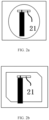
FIG. 6b is a schematic diagram of a slot that penetrates; -
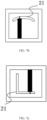
FIG. 7a is a schematic diagram of disposing of a slot; -
FIG. 7b is another schematic diagram of disposing of a slot; -
FIG. 7c is still another schematic diagram of disposing of a slot; -
FIG. 8 is a schematic diagram of connection between a tuning element and a feeding structure; -
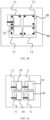
FIG. 9a is a schematic diagram when there are a plurality of shielding covers; -
FIG. 9b is another schematic diagram when there are a plurality of shielding covers; -
FIG. 9c is still another schematic diagram when there are a plurality of shielding covers; -
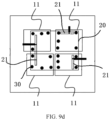
FIG. 9d is yet another schematic diagram when there are a plurality of shielding covers; and -
FIG. 10 is yet another schematic structural diagram of an electronic device according to an embodiment of this application. -
- shielding
cover 10;first metal layer 11;dielectric layer 12; -
second metal layer 20;slot 21; -
metal member 30;second metal member 32;third metal layer 33; - feeding
structure 40;flexible circuit board 51; - tuning
element 50;main board 60;radio frequency module 61; -
first antenna 70;second antenna 80;flexible circuit board 81; -
battery 90. - The following clearly and completely describes technical solutions in embodiments of this application with reference to accompanying drawings in the embodiments of this application. Apparently, the described embodiments are some but not all of the embodiments of this application. All other embodiments obtained by a person of ordinary skill in the art based on the embodiments of this application without creative efforts shall fall within the protection scope of this application.
- The terms "first", "second", and the like in this specification and claims of this application are used to distinguish between similar objects instead of describing a specific order or sequence. It should be understood that the data used in such a way is interchangeable in proper circumstances so that the embodiments of this application can be implemented in an order other than the order illustrated or described herein. In addition, in this specification and the claims, "and/or" represents at least one of connected objects, and a character "/" generally represents an "or" relationship between associated objects.
- With reference to
FIG. 1a to FIG. 10 , an electronic device provided in embodiments of this application is described in detail by using specific embodiments and application scenarios for the embodiments. - As shown in
FIG. 1a to FIG. 10 , the electronic device in the embodiments of this application includes a shieldingcover 10, asecond metal layer 20, ametal member 30, and a feedingstructure 40. The shieldingcover 10 is provided with afirst metal layer 11, and thefirst metal layer 11 may include at least one surface of the shieldingcover 10. The shieldingcover 10 may be soldered on a main grounding layer of a main board, and may perform electromagnetic shielding on a chip module or a discrete power amplifier component on the main board, which has a shielding function. Thefirst metal layer 11 may be located at the top of the shieldingcover 10, that is, a side away from the main board. - The
second metal layer 20 may be spaced apart from thefirst metal layer 11, and thesecond metal layer 20 and thefirst metal layer 11 may be disposed in parallel. The thickness of thesecond metal layer 20 may be 0.5 mm-2 mm. Thesecond metal layer 20 is disposed outside the shieldingcover 10. Thesecond metal layer 20 may be provided with aslot 21. A quantity of theslots 21 may be one or more. The quantity, a shape, and positions of theslots 21 may be selected based on an actual situation. Themetal member 30 may be disposed between thefirst metal layer 11 and thesecond metal layer 20, and themetal member 30 may form a resonant cavity in a manner of enclosing. Theslot 21 may be disposed at a position that is on thesecond metal layer 20 and that is corresponding to the resonant cavity. Themetal member 30 may extend in a circumferential direction of thesecond metal layer 20, and themetal member 30 may extend in an edge area of thesecond metal layer 20. Themetal member 30 may be circular or arc-shaped, and themetal member 30 may be electrically connected to thesecond metal layer 20 and thefirst metal layer 11 respectively. Thefirst metal layer 11 and thesecond metal layer 20 may form a first resonant cavity antenna. The feedingstructure 40 may be configured to feed the resonant cavity, and a signal may be fed to the resonant cavity by using the feedingstructure 40. A radio frequency signal may be radiated from theslot 21 after being subj ect to resonance of the resonant cavity, and an antenna with high radiation efficiency may be implemented above the shieldingcover 10. - In the electronic device in the embodiments of this application, the
metal member 30 is disposed between thefirst metal layer 11 of the shieldingcover 10 and thesecond metal layer 20, and themetal member 30 may form the resonant cavity in a manner of enclosing. Theslot 21 is provided on thesecond metal layer 20, and thefirst metal layer 11 and thesecond metal layer 20 form the first resonant cavity antenna, so that an antenna with high radiation efficiency may be disposed above the shieldingcover 10. An additional high-performance antenna is provided by using space above the shieldingcover 10, and the space above the shieldingcover 10 is fully used. Thefirst metal layer 11 in the shieldingcover 10 is used as a part of the first resonant cavity antenna. The shieldingcover 10 is integrated with the resonant cavity antenna, to provide extremely good structure consistency. An upper edge area of thesecond metal layer 20 in the resonant cavity antenna may be used as a support for another antenna, for example, may be used as a support for a near field communication (NFC) antenna, an ultra wide band (UWB) antenna, or a millimeter wave antenna, so that space is fully used. The resonant cavity antenna is implemented near the shielding cover 10 (with 0 clearance, low profile), so that extremely high radiation performance is provided, space for the entire electronic device is fully used, and more antennas are implemented. - In some embodiments, as shown in
FIG. 1b , themetal member 30 may extend in the circumferential direction of thesecond metal layer 20, and themetal member 30 may be located in an edge area of thefirst metal layer 11 and the edge area of thesecond metal layer 20. Themetal member 30 may be circular or arc-shaped. The resonant cavity may be formed by themetal member 30 between thefirst metal layer 11 and thesecond metal layer 20 in a manner of enclosing. The resonant cavity may be cylindrical, rectangular-cuboid-shaped, or cube-shaped. As shown inFIG. 1d , there may be a plurality ofmetal members 30, and themetal members 30 may be columnar or arc-shaped. The plurality ofmetal members 30 may be spaced apart from each other in a circumferential direction of thesecond metal layer 20, or may be evenly spaced apart from each other. The resonant cavity may be enclosed by the plurality ofmetal members 30 in a manner of enclosing. Themetal member 30 may be a non-closed annular metal sheet. As shown in a dashed line a inFIG. 6a , an opening may be provided on a part of a surface of themetal member 30, to implement mode adjustment and control of an antenna. - The
first metal layer 11, thesecond metal layer 20, and themetal member 30 may not be formed integrally. Themetal member 30 may be a metal elastic piece or a screw post. Thefirst metal layer 11 and thesecond metal layer 20 may be two discrete structural members. A position of the elastic piece may be flexibly adjusted based on an actual debugging condition, and a resonance frequency of the resonant cavity antenna is controlled. Debugging is performed efficiently for a short period, which avoids a problem that debugging is not easy to perform because of the integrated antenna structure, that the antenna structure needs to be replaced entirely, and that a sample is made for a long period. - In some other embodiments, as shown in
FIG. 3 , themetal member 30 may include a first metal member and asecond metal member 32. The first metal member may be electrically connected to thefirst metal layer 11 and thesecond metal layer 20 respectively. The first metal member may be disposed in a circumferential direction of thesecond metal layer 20, and forms a first resonant cavity in a manner of enclosing. The first metal member may extend in the circumferential direction of thesecond metal layer 20. The first metal member may be located in the edge area of thefirst metal layer 11 and the edge area of thesecond metal layer 20. The first metal member may be circular or arc-shaped. The first resonant cavity may be formed in a manner of enclosing by the first metal member between thefirst metal layer 11 and thesecond metal layer 20. The first resonant cavity may be cylindrical, rectangular-cuboid-shaped, or cube-shaped. There may be a plurality of first metal members, and the first metal members may be columnar or arc-shaped. The plurality of first metal members may be spaced apart from each other in the circumferential direction of thesecond metal layer 20, or may be evenly spaced apart from each other. The first resonant cavity may be formed by the plurality of first metal members in a manner of enclosing. - The
second metal member 32 is electrically connected to thefirst metal layer 11 and thesecond metal layer 20 respectively. Thesecond metal member 32 is disposed in the circumferential direction of thesecond metal layer 20 and forms a second resonant cavity in a manner of enclosing. The second resonant cavity is located in the first resonant cavity. Thesecond metal member 32 may extend in the circumferential direction of thesecond metal layer 20. Thesecond metal member 32 may be circular or arc-shaped. The second resonant cavity may be formed in a manner of enclosing by thesecond metal member 32 between thefirst metal layer 11 and thesecond metal layer 20. The second resonant cavity may be cylindrical, rectangular-cuboid-shaped, or cube-shaped. There may be a plurality ofsecond metal members 32. Thesecond metal member 32 may be cylindrical or arc-shaped. The plurality ofsecond metal members 32 may be spaced apart from each other in the circumferential direction of thesecond metal layer 20, or may be evenly spaced apart from each other. The second resonant cavity may be formed by the plurality ofsecond metal members 32 in a manner of enclosing. A plurality of high-order modes may be excited by using the first resonant cavity and the second resonant cavity, so that a frequency band covered by an antenna is expanded. - In an embodiment of this application, there may be a plurality of
second metal members 32, and thesecond metal members 32 may be distributed on two sides of theslot 21. Thesecond metal member 32 may be an elastic piece or a metal cylinder. Thesecond metal member 32 is connected to thefirst metal layer 11 and thesecond metal layer 20, to implement antenna mode control and implement broadband coverage. Thesecond metal member 32 is distributed on the two sides of theslot 21, so that the plurality of higher-order modes are excited for the antenna, and the frequency band covered by the antenna may be expanded. - In some embodiments, as shown in
FIG. 4 , adielectric layer 12 is filled between thefirst metal layer 11 and thesecond metal layer 20. Thedielectric layer 12 may be filled or partially filled in the resonant cavity, to reduce a resonance frequency of an antenna and reduce a length and width required for a cavity. Optionally, a loss tangent factor of thedielectric layer 12 may be less than 0.005. - In an embodiment of this application, as shown in
FIG. 9d , thesecond metal layer 20 may be provided with aplurality slots 21. The plurality ofslots 21 may be distributed at intervals. Specific intervals may be selected based on an actual condition. - Optionally, as shown in
FIG. 7a to FIG. 7c , theslot 21 may be strip-shaped, arc-shaped, annular, or L-shaped, and a plurality ofslots 21 cross each other to form cross-shaped slots. For example, as shown inFIG. 7a , two strip-shapedslots 21 cross each other to form a cross shape, which may be specifically selected based on an actual situation. Theslot 21 is used as a radiation caliber of an antenna, and a shape of theslot 21 is not limited to the foregoing shape. - Optionally, the
slot 21 may be located at an edge area of thesecond metal layer 20, to facilitate radiation of the antenna. Another antenna may be easily disposed at a central area of thesecond metal layer 20. For example, the central area may be reserved to be used by a UWB antenna or millimeter wave antenna. Therefore, layout is more proper. - Optionally, as shown in
FIG. 2a to FIG. 2c , the resonant cavity may be cylindrical, elliptic-cylinder-shaped, or polyhedron-shaped, and the resonant cavity may be a cavity of another shape formed by an arc line and a straight line. For example, the resonant cavity may be rectangular-cuboid-shaped, or cube-shaped, which may be specifically selected based on an actual situation, and may be correspondingly designed and adjusted based on an actual antenna mode, a bandwidth, and the like. - In some embodiments, a length of the
slot 21 may be half an operating wavelength of a radio frequency signal in a medium in theslot 21. - Optionally, the
slot 21 is strip-shaped, and a ratio of the length of theslot 21 to a width of theslot 21 may be greater than or equal to 10. - Optionally, as shown in
FIG. 6b , theslot 21 may extend inwardly from one side edge of thesecond metal layer 20 and penetrate from the other side edge of thesecond metal layer 20. Apart, provided with a slot, of thesecond metal layer 20 may extend to an edge, and thesecond metal layer 20 may be separated into two parts, so that a resonant cavity is divided into two half cavities. Sizes of the two half cavities may be equal or different, so that multi-frequency resonance may be implemented, and antenna impedance tuning may be performed. - In some embodiments, as shown in
FIG. 5a andFIG. 5b , the electronic device may further include athird metal layer 33. Thethird metal layer 33 may be disposed between thefirst metal layer 11 and thesecond metal layer 20, and thethird metal layer 33 is located in the resonant cavity. Thethird metal layer 33 may be spaced apart from thefirst metal layer 11 and thesecond metal layer 20 separately. Thethird metal layer 33 may be parallel to thefirst metal layer 11 and thesecond metal layer 20 separately. An edge of thethird metal layer 33 may be electrically connected to themetal member 30. Themetal member 30 may extend in the circumferential direction of thesecond metal layer 20. Thethird metal layer 33 may be rectangular-shaped. Thefirst metal layer 11, thesecond metal layer 20, and thethird metal layer 33 each may be rectangular-shaped. The resonant cavity may be rectangular-cuboid-shaped. Both of two adjacent edges of thethird metal layer 33 may be electrically connected to themetal member 30, and the other two adjacent edges of thethird metal layer 33 are not electrically connected to themetal member 30, and may be spaced apart from themetal member 30. Thethird metal layer 33 is parallel to thefirst metal layer 11 and thesecond metal layer 20, and thethird metal layer 33 may be connected to two surfaces of the resonant cavity, and is not connected to the other two surfaces, to form an L-shaped cavity part. Onethird metal layer 33 may be added to the inside of the resonant cavity, to implement folding of the resonant cavity, reduce an antenna resonance frequency, and reduce a length and width required for the cavity. - In some embodiments, as shown in
FIG. 9c , there may be a plurality of shielding covers 10, and there may be a plurality of second metal layers 20. Thefirst metal layer 11 of each shieldingcover 10 and one correspondingsecond metal layer 20 form the first resonant cavity antenna. For example, there may be four shielding covers 10, and there may be four second metal layers 20. Thefirst metal layer 11 of each shieldingcover 10 and one correspondingsecond metal layer 20 form the first resonant cavity antenna, that is, four first resonant cavity antennas are formed. Themetal member 30 is disposed between thefirst metal layer 11 of each shieldingcover 10 and the correspondingsecond metal layer 20, and themetal member 30 may form a resonant cavity in a manner of enclosing. Theslot 21 is provided on thesecond metal layer 20, and thefirst metal layer 11 of each shieldingcover 10 and thesecond metal layer 20 form the first resonant cavity antennas respectively, so that an antenna with high radiation efficiency may be disposed above the shieldingcover 10. A resonant cavity antenna is integrally designed above each shieldingcover 10, and a plurality of shielding covers 10 may be corresponding to a plurality of resonant cavity antennas. These resonant cavity antennas may operate in a same frequency band to implement a multiple input multiple output (Multiple Input Multiple Output, MIMO) antenna function, or operate in different frequency bands for a diversity antenna or MIMO antenna function with antennas of another type. - In some other embodiments, as shown in
FIG. 9a andFIG. 9b , there may be a plurality of shielding covers 10, for example, four, and there may be onesecond metal layer 20. All first metal layers on the plurality of shielding covers 10 and the second metal layers 20 are disposed correspondingly, to form the first resonant cavity antenna. For example, there are four shielding covers 10, and there is onesecond metal layer 20. Thesecond metal layer 20 may be rectangular-shaped. The four shielding covers 10 may be respectively located at corners of thesecond metal layer 20. The first metal layers 11 on the four shielding covers 10 and the second metal layers 20 are disposed correspondingly, to form the first resonant cavity antennas. - As shown in
FIG. 9a andFIG. 9b , the first metal layers 11 on the plurality of shielding covers 10 are jointly corresponding to one largesecond metal layer 20, to cope with a situation in which an operation frequency of an antenna needs to be relatively low. Themetal members 30, such as metal elastic pieces, may be disposed above the plurality of shielding covers 10. Themetal member 30 may be electrically connected to thesecond metal layer 20 to form one first resonant cavity antenna, to cope with the situation in which the operation frequency of the antenna needs to be relatively low. In this implementation, debugging is relatively more flexible. Themetal member 30 may be a screw post, and thefirst metal layer 11 on the shieldingcover 10 may be electrically connected to thesecond metal layer 20 in a screw locking manner. - In an embodiment of this application, as shown in
FIG. 9d , a plurality of resonant cavities may be formed between thefirst metal layer 11 and thesecond metal layer 20, for example, three resonant cavities.Slots 21 are respectively disposed at positions, corresponding to the resonant cavities, of thesecond metal layer 20, to implement flexible layout of the plurality of antennas. Themetal members 30 may be disposed above the plurality of shielding covers 10, and themetal members 30 may be metal elastic pieces. Through reasonable layout of the elastic pieces, thefirst metal layer 11 is electrically connected to thesecond metal layer 20, and different resonant cavities are formed by division. Threeslots 21 may be provided on thesecond metal layer 20 to be respectively corresponding to antenna radiation calibers of the resonant cavities, thereby implementing flexible layout of the plurality of antennas. For example, there are four shielding covers 10, and there is onesecond metal layer 20. Thesecond metal layer 20 may be rectangular-shaped. The four shielding covers 10 may be respectively located at corners of thesecond metal layer 20. Three resonant cavities are formed between the first metal layers 11 on the four shielding covers 10 and thesecond metal layer 20 respectively, and aslot 21 may be disposed at a position, corresponding to each resonant cavity, on thesecond metal layer 20, to implement flexible layout of the plurality of antennas. - In some embodiments, as shown in
FIG. 1a to FIG. 1d , the electronic device may further include a feedingstructure 40. The feedingstructure 40 is configured to feed the resonant cavity. The feedingstructure 40 may include a coaxial line. The resonant cavity may be fed by using one coaxial line. One end of the coaxial line may be connected to a baseband and theradio frequency module 61. An inner core of the other end of the coaxial line may be connected to one side of theslot 21, and an outer grounding layer may be connected to the other side of theslot 21. - The
slot 21 of the resonant cavity antenna may perform feeding in a coupling feeding manner by using aflexible circuit board 51, or thesecond metal layer 20 may be fed in a coupling feeding manner through theflexible circuit board 51. As shown inFIG. 8 , the coaxial line in the feedingstructure 40 may be connected to theflexible circuit board 51, and an end of theflexible circuit board 51 may be electrically connected to one end of atuning element 50, and the other end of thetuning element 50 is connected to one side of theslot 21, so that an antenna adjustment freedom can be increased. A shape of theflexible circuit board 51 and a value of an electronic element are modified, to implement multi-frequency tuning and optimize antenna impedance, making debugging more flexible. - In some embodiments, as shown in
FIG. 8 , the electronic device may further include thetuning element 50. The feedingstructure 40 feeds the resonant cavity by using thetuning element 50. The tuning element may include the electronic element. The electronic element may be a capacitor, an inductor, or a switch component. There are no less than two electronic elements. Multi-frequency tuning can be implemented by using the tuning element, and antenna impedance can be optimized. - Optionally, as shown in
FIG. 1a ,FIG. 1c , andFIG. 10 , the electronic device may further include amain board 60. The shieldingcover 10 may be disposed on themain board 60. The shieldingcover 10 may be soldered on a main grounding layer of themain board 60, and may perform electromagnetic shielding on a chip module or a discrete power amplifier component on themain board 60. Thefirst metal layer 11 may be located at the top of the shieldingcover 10, that is, a side away from the main board. - In some embodiments, as shown in
FIG. 10 , the electronic device may further include afirst antenna 70. Thefirst antenna 70 may be disposed on thesecond metal layer 20. The shieldingcover 10 may be located in a middle of themain board 60, and may be located at a position at which a chip shielding cover is located. Because a radiation caliber (at a slot) is on an edge of thesecond metal layer 20, actual occupied space is extremely small, and it may be considered that the entire structure is reused. In addition, thesecond metal layer 20 may further be used as a support. Thesecond metal layer 20 may be used as a support for thefirst antenna 70. Thefirst antenna 70 may include at least one of a UWB antenna, an NFC antenna, and a millimeter wave antenna. In this way, an antenna may be additionally disposed at an area in which a conventional antenna design is forbidden, thereby improving spatial utilization. - In some other embodiments, as shown in
FIG. 10 , the electronic device may further includesecond antennas 80. Thesecond antenna 80 may be disposed at an edge area of the electronic device. Thesecond antenna 80 may include an antenna in a frequency band less than 6 GHz such as a cellular (cellular) antenna and a WiFi (WIFI) antenna. Thesecond antenna 80 is arranged at an edge position of the electronic device to facilitate radiation, thereby improving antenna performance. The electronic device may further include aflexible circuit board 81. For example, thesecond antenna 80 may be fed through theflexible circuit board 81. - In some embodiments, as shown in
FIG. 10 , the electronic device may further include abattery 90 and a back cover. Thebattery 90 and the back cover may be spaced apart from each other in a thickness direction of thebattery 90. A second resonant cavity antenna may be disposed between thebattery 90 and the back cover, and a metal layer on thebattery 90 may be used to form the second resonant cavity antenna. Space between thebattery 90 and the back cover may be fully used, thereby improving space utilization, increasing a quantity of antennas, and improving entire antenna performance. - In some other embodiments, the electronic device may further include a display screen and a frame. The display screen may be disposed on the frame, and a third resonant cavity antenna may be disposed between the display screen and the frame, so that space between the display screen and the frame may be fully used, space utilization is improved, a quantity of antennas may be increased, and the overall antenna performance can be enhanced.
- The embodiments of this application are described above with reference to the accompanying drawings, but this application is not limited to the foregoing implementations, and the foregoing specific implementations are only illustrative and not restrictive. Under the enlightenment of this application, a person of ordinary skill in the art can make many forms without departing from the purpose of this application and the protection scope of the claims, all of which fall within the protection of this application.
Claims (14)
- An electronic device, comprising:a shielding cover, wherein the shielding cover is provided with a first metal layer;a second metal layer, wherein the second metal layer is spaced apart from the first metal layer, a slot is provided on the second metal layer, and the second metal layer is disposed outside the shielding cover;a metal member, wherein the metal member is disposed between the first metal layer and the second metal layer, the metal member forms a resonant cavity in a manner of enclosing, the metal member is electrically connected to the first metal layer and the second metal layer separately, and the first metal layer and the second metal layer form a first resonant cavity antenna; anda feeding structure, wherein the feeding structure is configured to feed the resonant cavity.
- The electronic device according to claim 1, wherein the metal member extends in a circumferential direction of the second metal layer; or
there are a plurality of metal members, and the plurality of metal members are spaced apart from each other in a circumferential direction of the second metal layer. - The electronic device according to claim 1, wherein the metal member comprises:a first metal member, wherein the first metal member is electrically connected to the first metal layer and the second metal layer separately, and the first metal member is disposed in a circumferential direction of the second metal layer, and forms a first resonant cavity in a manner of enclosing; anda second metal member, wherein the second metal member is electrically connected to the first metal layer and the second metal layer separately, the second metal member is disposed in the circumferential direction of the second metal layer and forms a second resonant cavity in a manner of enclosing, and the second resonant cavity is located in the first resonant cavity.
- The electronic device according to claim 3, wherein there are a plurality of second metal members, and the second metal members are distributed on two sides of the slot.
- The electronic device according to claim 1, wherein a dielectric layer is filled between the first metal layer and the second metal layer.
- The electronic device according to claim 1, wherein the slot is strip-shaped, and a ratio of a length of the slot to a width of the slot is greater than or equal to 10.
- The electronic device according to claim 1, further comprising:
a third metal layer, wherein the third metal layer is disposed between the first metal layer and the second metal layer and is located in the resonant cavity, the third metal layer is spaced apart from the first metal layer and the second metal layer separately, and an edge of the third metal layer is electrically connected to the metal member. - The electronic device according to claim 7, wherein the metal member extends in a circumferential direction of the second metal layer, the third metal layer is rectangular-shaped, and two adjacent edges of the third metal layer are both electrically connected to the metal member.
- The electronic device according to claim 1, wherein there are a plurality of shielding covers, there are a plurality of second metal layers, and a first metal layer of each shielding cover and one corresponding second metal layer form one of the first resonant cavity antennas.
- The electronic device according to claim 1, wherein there are a plurality of shielding covers, there is one second metal layer, and first metal layers on the plurality of shielding covers are all disposed corresponding to the second metal layer to form the first resonant cavity antennas respectively.
- The electronic device according to claim 1 or 10, wherein a plurality of the resonant cavities are formed between the first metal layer and the second metal layer, and the slots are respectively disposed at positions, corresponding to the resonant cavities, on the second metal layer.
- The electronic device according to claim 1, further comprising:
a tuning element, wherein the feeding structure feeds the resonant cavity by using the tuning element. - The electronic device according to claim 1, further comprising:
a main board, wherein the shielding cover is disposed on the main board. - The electronic device according to claim 1, further comprising:
a first antenna, wherein the first antenna is disposed on the second metal layer.
Applications Claiming Priority (2)
| Application Number | Priority Date | Filing Date | Title |
|---|---|---|---|
| CN202111220072.3A CN113964483B (en) | 2021-10-20 | 2021-10-20 | electronic devices |
| PCT/CN2022/125923 WO2023066249A1 (en) | 2021-10-20 | 2022-10-18 | Electronic device |
Publications (2)
| Publication Number | Publication Date |
|---|---|
| EP4421980A1 true EP4421980A1 (en) | 2024-08-28 |
| EP4421980A4 EP4421980A4 (en) | 2025-03-05 |
Family
ID=79465494
Family Applications (1)
| Application Number | Title | Priority Date | Filing Date |
|---|---|---|---|
| EP22882854.7A Pending EP4421980A4 (en) | 2021-10-20 | 2022-10-18 | Electronic device |
Country Status (4)
| Country | Link |
|---|---|
| US (1) | US20240266747A1 (en) |
| EP (1) | EP4421980A4 (en) |
| CN (1) | CN113964483B (en) |
| WO (1) | WO2023066249A1 (en) |
Families Citing this family (8)
| Publication number | Priority date | Publication date | Assignee | Title |
|---|---|---|---|---|
| CN113964483B (en) * | 2021-10-20 | 2025-10-31 | 维沃移动通信有限公司 | electronic devices |
| CN115377664B (en) * | 2022-08-31 | 2025-05-02 | 维沃移动通信有限公司 | An electronic device |
| TWI844221B (en) * | 2023-01-05 | 2024-06-01 | 啟碁科技股份有限公司 | Antenna structure and mobile device having the same |
| CN116742333A (en) * | 2023-04-14 | 2023-09-12 | 维沃移动通信有限公司 | Electronic equipment |
| CN116315644A (en) * | 2023-04-21 | 2023-06-23 | 北京小米移动软件有限公司 | Antennas and Electronics |
| CN116598750B (en) * | 2023-06-19 | 2026-04-21 | 维沃移动通信有限公司 | Antenna modules and electronic devices |
| CN116581519A (en) * | 2023-06-30 | 2023-08-11 | 维沃移动通信有限公司 | Electronic equipment |
| CN116914420A (en) * | 2023-08-23 | 2023-10-20 | 维沃移动通信有限公司 | Antenna device |
Family Cites Families (14)
| Publication number | Priority date | Publication date | Assignee | Title |
|---|---|---|---|---|
| JP2004015160A (en) * | 2002-06-04 | 2004-01-15 | Tdk Corp | Module with antenna |
| US20070080864A1 (en) * | 2005-10-11 | 2007-04-12 | M/A-Com, Inc. | Broadband proximity-coupled cavity backed patch antenna |
| US8847842B2 (en) * | 2011-11-14 | 2014-09-30 | Continental Automotive Systems, Inc. | GPS antenna on-shield/housing with grounding |
| US9716307B2 (en) * | 2012-11-08 | 2017-07-25 | Htc Corporation | Mobile device and antenna structure |
| CN105449355A (en) * | 2015-12-26 | 2016-03-30 | 昆山联滔电子有限公司 | Antenna device |
| US10854953B2 (en) * | 2017-09-27 | 2020-12-01 | Apple Inc. | Electronic devices having housing-integrated antennas |
| CN110544822B (en) * | 2018-11-16 | 2020-08-25 | 西安电子科技大学 | Ka-band miniaturized filtering antenna based on SIW structure |
| CN210040545U (en) * | 2019-06-27 | 2020-02-07 | 昆山昕芮特电子科技有限公司 | GPRS dual-band PIFA antenna |
| KR102721294B1 (en) * | 2019-11-08 | 2024-10-23 | 엘지전자 주식회사 | Slot Antenna |
| US11303039B2 (en) * | 2020-05-28 | 2022-04-12 | The Boeing Company | Electromagnetic radiators with ground planes having discontinuities |
| CN213936550U (en) * | 2020-09-09 | 2021-08-10 | 深圳市信维通信股份有限公司 | Medium-loaded miniaturized ultra-wideband antenna structure and electronic equipment |
| CN112993579B (en) * | 2021-02-08 | 2023-07-25 | Oppo广东移动通信有限公司 | Antenna devices and electronic equipment |
| CN113054425B (en) * | 2021-03-17 | 2022-10-14 | 东南大学 | Millimeter wave dual-frequency dual-polarization filtering antenna |
| CN113964483B (en) * | 2021-10-20 | 2025-10-31 | 维沃移动通信有限公司 | electronic devices |
-
2021
- 2021-10-20 CN CN202111220072.3A patent/CN113964483B/en active Active
-
2022
- 2022-10-18 EP EP22882854.7A patent/EP4421980A4/en active Pending
- 2022-10-18 WO PCT/CN2022/125923 patent/WO2023066249A1/en not_active Ceased
-
2024
- 2024-04-18 US US18/639,490 patent/US20240266747A1/en active Pending
Also Published As
| Publication number | Publication date |
|---|---|
| CN113964483A (en) | 2022-01-21 |
| WO2023066249A1 (en) | 2023-04-27 |
| EP4421980A4 (en) | 2025-03-05 |
| CN113964483B (en) | 2025-10-31 |
| US20240266747A1 (en) | 2024-08-08 |
Similar Documents
| Publication | Publication Date | Title |
|---|---|---|
| US20240266747A1 (en) | Electronic device | |
| EP3767742B1 (en) | Antenna device and mobile terminal | |
| US9123990B2 (en) | Multi-feed antenna apparatus and methods | |
| EP4152517B1 (en) | Terminal antenna and terminal electronic device | |
| EP3035442B1 (en) | Antenna and mobile terminal | |
| US8866689B2 (en) | Multi-band antenna and methods for long term evolution wireless system | |
| US10062949B2 (en) | Integrated multi-band bandpass filters based on dielectric resonators for mobile and other communication devices and applications | |
| US8164537B2 (en) | Multiband folded dipole transmission line antenna | |
| EP3246989B1 (en) | Multi-frequency antenna and terminal device | |
| US20180183132A1 (en) | Multi-antenna communication device | |
| EP3300170B1 (en) | Antenna and user equipment | |
| EP3852194B1 (en) | Terminal device antenna | |
| EP3910737A1 (en) | Antenna structure | |
| CN107078387B (en) | A kind of multi-frequency antenna and terminal equipment | |
| EP3852195B1 (en) | Terminal device antenna | |
| EP2760079B1 (en) | Pcb applied in wireless terminal and wireless terminal | |
| EP4697497A1 (en) | Electronic device | |
| EP4557515A1 (en) | Antenna assembly and electronic device | |
| Al-Tamimi | Design of elliptical shaped multiband antenna for application in wireless communication | |
| US11955712B2 (en) | Self-decoupled compact cavity antenna | |
| US11095320B2 (en) | Communication system and communication method | |
| Awan et al. | Reconfigurable antenna for 4G LTE and 5G applications | |
| Sarsamba et al. | T-slot reconfigurable micro-strip patch antenna with capacitive loading technique for wimax and s-band application | |
| EP4195411B1 (en) | Communication device | |
| Singh et al. | A hexa-band frequency reconfigurable patch antenna for wireless applications |
Legal Events
| Date | Code | Title | Description |
|---|---|---|---|
| STAA | Information on the status of an ep patent application or granted ep patent |
Free format text: STATUS: THE INTERNATIONAL PUBLICATION HAS BEEN MADE |
|
| PUAI | Public reference made under article 153(3) epc to a published international application that has entered the european phase |
Free format text: ORIGINAL CODE: 0009012 |
|
| STAA | Information on the status of an ep patent application or granted ep patent |
Free format text: STATUS: REQUEST FOR EXAMINATION WAS MADE |
|
| 17P | Request for examination filed |
Effective date: 20240515 |
|
| AK | Designated contracting states |
Kind code of ref document: A1 Designated state(s): AL AT BE BG CH CY CZ DE DK EE ES FI FR GB GR HR HU IE IS IT LI LT LU LV MC ME MK MT NL NO PL PT RO RS SE SI SK SM TR |
|
| DAV | Request for validation of the european patent (deleted) | ||
| DAX | Request for extension of the european patent (deleted) | ||
| REG | Reference to a national code |
Ref country code: DE Ref legal event code: R079 Free format text: PREVIOUS MAIN CLASS: H01Q0001240000 Ipc: H01Q0013180000 |
|
| A4 | Supplementary search report drawn up and despatched |
Effective date: 20250204 |
|
| RIC1 | Information provided on ipc code assigned before grant |
Ipc: H01Q 1/52 20060101ALI20250129BHEP Ipc: H05K 9/00 20060101ALI20250129BHEP Ipc: H01Q 13/18 20060101AFI20250129BHEP |