EP4421876A1 - Thyristor and method for manufacturing same - Google Patents
Thyristor and method for manufacturing same Download PDFInfo
- Publication number
- EP4421876A1 EP4421876A1 EP22877674.6A EP22877674A EP4421876A1 EP 4421876 A1 EP4421876 A1 EP 4421876A1 EP 22877674 A EP22877674 A EP 22877674A EP 4421876 A1 EP4421876 A1 EP 4421876A1
- Authority
- EP
- European Patent Office
- Prior art keywords
- type semiconductor
- semiconductor layer
- layer
- thyristor
- junction
- Prior art date
- Legal status (The legal status is an assumption and is not a legal conclusion. Google has not performed a legal analysis and makes no representation as to the accuracy of the status listed.)
- Pending
Links
- 238000004519 manufacturing process Methods 0.000 title claims description 12
- 238000000034 method Methods 0.000 title description 6
- 239000004065 semiconductor Substances 0.000 claims abstract description 320
- 239000012535 impurity Substances 0.000 claims abstract description 40
- 230000035945 sensitivity Effects 0.000 abstract description 20
- 230000007257 malfunction Effects 0.000 description 7
- VYPSYNLAJGMNEJ-UHFFFAOYSA-N Silicium dioxide Chemical compound O=[Si]=O VYPSYNLAJGMNEJ-UHFFFAOYSA-N 0.000 description 6
- 230000002159 abnormal effect Effects 0.000 description 6
- 238000000151 deposition Methods 0.000 description 5
- 229910052681 coesite Inorganic materials 0.000 description 3
- 229910052906 cristobalite Inorganic materials 0.000 description 3
- 230000000694 effects Effects 0.000 description 3
- 238000002161 passivation Methods 0.000 description 3
- 239000000377 silicon dioxide Substances 0.000 description 3
- 229910052682 stishovite Inorganic materials 0.000 description 3
- 229910052905 tridymite Inorganic materials 0.000 description 3
- 238000010586 diagram Methods 0.000 description 2
- 239000011521 glass Substances 0.000 description 2
- 238000002955 isolation Methods 0.000 description 2
- 238000005192 partition Methods 0.000 description 1
Images


Classifications
-
- H—ELECTRICITY
- H10—SEMICONDUCTOR DEVICES; ELECTRIC SOLID-STATE DEVICES NOT OTHERWISE PROVIDED FOR
- H10D—INORGANIC ELECTRIC SEMICONDUCTOR DEVICES
- H10D62/00—Semiconductor bodies, or regions thereof, of devices having potential barriers
- H10D62/10—Shapes, relative sizes or dispositions of the regions of the semiconductor bodies; Shapes of the semiconductor bodies
- H10D62/124—Shapes, relative sizes or dispositions of the regions of semiconductor bodies or of junctions between the regions
- H10D62/126—Top-view geometrical layouts of the regions or the junctions
-
- H—ELECTRICITY
- H10—SEMICONDUCTOR DEVICES; ELECTRIC SOLID-STATE DEVICES NOT OTHERWISE PROVIDED FOR
- H10D—INORGANIC ELECTRIC SEMICONDUCTOR DEVICES
- H10D18/00—Thyristors
- H10D18/01—Manufacture or treatment
-
- H—ELECTRICITY
- H10—SEMICONDUCTOR DEVICES; ELECTRIC SOLID-STATE DEVICES NOT OTHERWISE PROVIDED FOR
- H10D—INORGANIC ELECTRIC SEMICONDUCTOR DEVICES
- H10D18/00—Thyristors
-
- H—ELECTRICITY
- H10—SEMICONDUCTOR DEVICES; ELECTRIC SOLID-STATE DEVICES NOT OTHERWISE PROVIDED FOR
- H10D—INORGANIC ELECTRIC SEMICONDUCTOR DEVICES
- H10D18/00—Thyristors
- H10D18/60—Gate-turn-off devices
-
- H—ELECTRICITY
- H10—SEMICONDUCTOR DEVICES; ELECTRIC SOLID-STATE DEVICES NOT OTHERWISE PROVIDED FOR
- H10D—INORGANIC ELECTRIC SEMICONDUCTOR DEVICES
- H10D62/00—Semiconductor bodies, or regions thereof, of devices having potential barriers
- H10D62/10—Shapes, relative sizes or dispositions of the regions of the semiconductor bodies; Shapes of the semiconductor bodies
- H10D62/13—Semiconductor regions connected to electrodes carrying current to be rectified, amplified or switched, e.g. source or drain regions
- H10D62/141—Anode or cathode regions of thyristors; Collector or emitter regions of gated bipolar-mode devices, e.g. of IGBTs
- H10D62/148—Cathode regions of thyristors
-
- H—ELECTRICITY
- H10—SEMICONDUCTOR DEVICES; ELECTRIC SOLID-STATE DEVICES NOT OTHERWISE PROVIDED FOR
- H10D—INORGANIC ELECTRIC SEMICONDUCTOR DEVICES
- H10D62/00—Semiconductor bodies, or regions thereof, of devices having potential barriers
- H10D62/10—Shapes, relative sizes or dispositions of the regions of the semiconductor bodies; Shapes of the semiconductor bodies
- H10D62/17—Semiconductor regions connected to electrodes not carrying current to be rectified, amplified or switched, e.g. channel regions
- H10D62/192—Base regions of thyristors
- H10D62/206—Cathode base regions of thyristors
-
- H—ELECTRICITY
- H10—SEMICONDUCTOR DEVICES; ELECTRIC SOLID-STATE DEVICES NOT OTHERWISE PROVIDED FOR
- H10D—INORGANIC ELECTRIC SEMICONDUCTOR DEVICES
- H10D62/00—Semiconductor bodies, or regions thereof, of devices having potential barriers
- H10D62/60—Impurity distributions or concentrations
-
- H—ELECTRICITY
- H10—SEMICONDUCTOR DEVICES; ELECTRIC SOLID-STATE DEVICES NOT OTHERWISE PROVIDED FOR
- H10D—INORGANIC ELECTRIC SEMICONDUCTOR DEVICES
- H10D62/00—Semiconductor bodies, or regions thereof, of devices having potential barriers
- H10D62/10—Shapes, relative sizes or dispositions of the regions of the semiconductor bodies; Shapes of the semiconductor bodies
- H10D62/113—Isolations within a component, i.e. internal isolations
- H10D62/114—PN junction isolations
-
- H—ELECTRICITY
- H10—SEMICONDUCTOR DEVICES; ELECTRIC SOLID-STATE DEVICES NOT OTHERWISE PROVIDED FOR
- H10D—INORGANIC ELECTRIC SEMICONDUCTOR DEVICES
- H10D62/00—Semiconductor bodies, or regions thereof, of devices having potential barriers
- H10D62/10—Shapes, relative sizes or dispositions of the regions of the semiconductor bodies; Shapes of the semiconductor bodies
- H10D62/113—Isolations within a component, i.e. internal isolations
- H10D62/115—Dielectric isolations, e.g. air gaps
Definitions
- the present invention relates to a thyristor and a method for manufacturing the same.
- a conventional thyristor is used in a protection circuit to prevent an inrush current when an LED light is turned on.
- Various aspects of the present invention have an object to provide a thyristor with desensitized gate sensitivity and a method for manufacturing the same.
- the third P-type semiconductor layer which is connected to the gate electrode and has an impurity concentration higher than that of the second P-type semiconductor layer
- the fourth P-type semiconductor layer which is in contact with each of the second P-type semiconductor layer and the second N-type semiconductor layer, is disposed below the cathode electrode, and has an impurity concentration higher than that of the second P-type semiconductor layer, are provided, it is possible to desensitize the gate sensitivity of the thyristor.
- the fourth P-type semiconductor layer is disposed on the third P-type semiconductor layer side in plan view, it is possible to further desensitize the gate sensitivity of the thyristor.
- the first PN junction is located closer to the gate electrode side than the second PN junction in plan view, it is possible to further desensitize the gate sensitivity of the thyristor.
- the fourth P-type semiconductor layer is disposed so as to cover a part of the bottom portion of the second N-type semiconductor layer and the side portion of the second N-type semiconductor layer on the gate electrode side, it is possible to further desensitize the gate sensitivity of the thyristor.
- Fig. 1 is a cross-sectional view showing a thyristor according to one aspect of the invention.
- Fig. 2A is a plan view of a fourth P-type semiconductor layer (second second base layer: P ++ ) 15b on the surface side of the thyristor shown in Fig. 1
- Fig. 2B is a plan view showing a second N-type semiconductor layer (emitter layer: N + ) 14 on the surface side of the thyristor shown in Fig. 1 .
- N + N-type semiconductor layer
- the thyristor of the above [1] includes: a first P-type semiconductor layer (P + ) 11; a first N-type semiconductor layer (N - ) 12 that is disposed in contact with the first P-type semiconductor layer (P + ) 11 and is separated from the first P-type semiconductor layer (P + ) 11; a second P-type semiconductor layer (P + ) 13 disposed in contact with the first N-type semiconductor layer (N - ) 12; a second N-type semiconductor layer (N + ) 14 disposed in contact with the second P-type semiconductor layer 13; a third P-type semiconductor layer (P ++ ) 15a that is disposed in contact with the second P-type semiconductor layer (P + ) 13 and has an impurity concentration higher than that of the second P-type semiconductor layer (P + ) 13; a gate electrode G electrically connected to the third P-type semiconductor layer (P ++ ) 15a; a cathode electrode K electrically connected to the second N-type semiconductor
- the third P-type semiconductor layer (P ++ ) 15a and the fourth P-type semiconductor layer (P ++ ) 15b are separated from each other by the second P-type semiconductor layer (P + ) 13, and the third P-type semiconductor layer (P ++ ) 15a and the second N-type semiconductor layer (N + ) 14 are separated from each other by the second P-type semiconductor layer (P + ) 13.
- the thyristor shown in Fig. 1 has an N-type semiconductor wafer 9, and the N-type semiconductor wafer 9 has the first P-type semiconductor layer (P + ) 11.
- Figs. 1, 2A and 2B show one thyristor chip after the N-type semiconductor wafer 9 is cut by dicing.
- the first N-type semiconductor layer (N - ) 12 is disposed so as to be in contact with the first P-type semiconductor layer (P + ) 11.
- the second P-type semiconductor layer (first base layer: P + ) 13 is disposed so as to be in contact with the first N-type semiconductor layer (N - ) 12.
- the concentrations of the first P-type semiconductor layer (P + ) 11 and the second P-type semiconductor layer (P + ) 13 may be the same, or either may be higher.
- the concentration range of each of the first P-type semiconductor layer (P + ) 11 and the second P-type semiconductor layer (P + ) 13 may be between 1 ⁇ 10 16 atoms ⁇ cm -3 and 5 ⁇ 10 18 atoms ⁇ cm -3 .
- the second N-type semiconductor layer (emitter layer: N + ) 14 is disposed so as to be in contact with the second P-type semiconductor layer (first base layer: P + ) 13.
- the planar shape of the emitter layer (N + ) 14 is shown in Fig. 2B .
- the third P-type semiconductor layer (first second base layer: P ++ ) 15a is disposed so as to be in contact with the second P-type semiconductor layer (first base layer: P + ) 13.
- the first second base layer (P ++ ) 15a has a higher impurity concentration than the first base layer (P + ) 13.
- a gate electrode G is electrically connected on the third P-type semiconductor layer (P ++ ) 15a.
- the gate electrode G is preferably formed of Al.
- a cathode electrode K is electrically connected on the second N-type semiconductor layer (N + ) 14.
- the cathode electrode K is preferably formed of Al.
- the fourth P-type semiconductor layer (second second base layer: P ++ ) 15b in contact with each of the first base layer 13 and the second N-type semiconductor layer (emitter layer: N + ) 14 is disposed.
- the second second base layer (P ++ ) 15b is disposed below the cathode electrode K (see Figs. 2A, 2B and 3 ).
- the second second base layer (P ++ ) 15 b has a higher impurity concentration than the first base layer (P + ) 13.
- the planar shape of the second second base layer (P ++ ) 15b is shown in Fig. 2A .
- the third P-type semiconductor layer (first second base layer: P ++ ) 15a and the fourth P-type semiconductor layer (second second base layer: P ++ ) 15b are separated from each other by the second P-type semiconductor layer (first base layer: P + ) 13.
- the first second base layer (P ++ ) 15a and the second N-type semiconductor layer (emitter layer: N + ) 14 are separated from each other by the first base layer (P + ) 13.
- an SiO 2 film 21 is formed on the emitter layer (N + ) 14, the first base layer (P + ) 13, and the first second base layer (P ++ ) 15a.
- the cathode electrode K is formed on the emitter layer (N + ) 14 and the SiO 2 film 21.
- the gate electrode G is formed on the first second base layer (P ++ ) 15a and the SiO 2 film 21.
- a glass passivation film 22 is formed at each end of the first N-type semiconductor layer (N - ) 12, the first base layer (P + ) 13, the emitter layer (N + ) 14, and the first second base layer (P ++ ) 15a.
- the glass passivation film 22a is formed between the cathode electrode K and the gate electrode G.
- the first second base layer (P ++ ) 15a which is connected to the gate electrode G and has an impurity concentration higher than that of the first base layer (P + ) 13, and the second second base layer (P ++ ) 15b, which is in contact with each of the first base layer (P + ) 13 and the emitter layer (N + ) 14, is disposed below the cathode electrode K, and has an impurity concentration higher than that of the first base layer (P + ) 13, are provided, it is possible to desensitize the gate sensitivity of the thyristor.
- first second base layer (P ++ ) 15a and the second second base layer (P ++ ) 15b are separated from each other by the first base layer 13, it is possible to further desensitize the gate sensitivity of the thyristor.
- a thyristor requires a G (gate) current to turn on between A and K (between the anode A and the cathode K).
- G gate
- a depletion layer at a junction between the first N-type semiconductor layer (N - ) 12 and the first base layer (P + ) 13 shown in Fig. 1 expands. This is the capacitance C of a condenser. Electrons move inside the thyristor to charge the capacitance C of the condenser. This charge current behaves the same as the G current.
- Fig. 6 is a diagram showing the dv/dt resistance of each thyristor sample of a structure 1 of the invention, a structure 2 of the invention, and a conventional structure.
- the structure 1 of the invention and the structure 2 of the invention are thyristors having the structure shown in Fig. 1 .
- the structure 2 of the invention is only different from the structure 1 of the invention in that the ratio of the area of the second second base layer (P ++ ) 15b shown in Fig. 2A in contact with the emitter layer (N + ) 14 to the area of the emitter layer (N + ) 14 shown in Fig. 2B in the thyristor according to one aspect of the invention shown in Fig.
- the conventional structure is different from the structure 1 of the invention and the structure 2 of the invention in that there is no second second base layer (P ++ ) 15b shown in Fig. 1 , and the other points are the same.
- the fourth P-type semiconductor layer (second second base layer: P ++ ) 15b is disposed on the third P-type semiconductor layer (first second base layer: P ++ ) 15a side (see Figs. 1, 2A, 2B , 3, 4A and 4B ). In this manner, it is possible to further desensitize the gate sensitivity of the thyristor.
- a first PN junction is formed between the fourth P-type semiconductor layer (second second base layer: P ++ ) 15b and a part 14a of a bottom portion of the second N-type semiconductor layer (emitter layer: N + ) 14.
- a second PN junction is formed between the second P-type semiconductor layer (first base layer: P + ) 13 and a bottom portion 14c of the emitter layer (N + ) 14 other than the part 14a of the bottom portion.
- the first PN junction is located closer to the gate electrode G side than the second PN junction (see Fig. 1 ). In this manner, it is possible to further desensitize the gate sensitivity of the thyristor. As a result, even when this thyristor is used in a protection circuit for preventing an inrush current when an LED light is turned on, for example, it is possible to suppress an abnormal operation of the protection circuit for preventing an inrush current or the occurrence of malfunction due to minute noise. In addition to this, the critical off-voltage rise rate dv/dt resistance also increases.
- the fourth P-type semiconductor layer (second second base layer: P ++ ) 15b is disposed so as to cover the part 14a of the bottom portion of the second N-type semiconductor layer (emitter layer: N + ) 14 and a side portion 14b on the gate electrode G side. In this manner, it is possible to further desensitize the gate sensitivity of the thyristor. Therefore, even when this thyristor is used in a protection circuit for preventing an inrush current when an LED light is turned on, for example, it is possible to suppress an abnormal operation of the protection circuit for preventing an inrush current or the occurrence of malfunction due to minute noise. In addition to this, the critical off-voltage rise rate dv/dt resistance also increases.
- Fig. 5 is a partial cross-sectional view of the vicinity of the emitter layer (N + ) 14 enlarged to explain the impurity concentration of the second N-type semiconductor layer (emitter layer: N + ) 14 in the thyristor shown in Fig. 1 .
- the impurity concentration of the second N-type semiconductor layer (emitter layer: N + ) 14 is higher in a portion in contact with the fourth P-type semiconductor layer (second second base layer: P ++ ) 15b than in a portion not in contact with the fourth P-type semiconductor layer (second second base layer: P ++ ) 15b.
- the impurity concentration of the second N-type semiconductor layer (N ++ ) 14 located on the second second base layer (P ++ ) 15b is higher than the impurity concentration of the second N-type semiconductor layer (N + ) 14 below which the second second base layer (P ++ ) 15b is not present.
- this semiconductor device has a structure including the second N-type semiconductor layer (N ++ ) 14, the second second base layer (P ++ ) 15b, and an NPN-Tr at a junction between the second P-type semiconductor layer (first base layer: P + ) 13 and the first N-type semiconductor layer (N - ) 12.
- the ratio of the area of the fourth P-type semiconductor layer (second second base layer: P ++ ) 15b in contact with the second N-type semiconductor layer (N + ) 14 to the area of the second N-type semiconductor layer (emitter layer: N + ) 14 is preferably 10% or more and 99% or less.
- this thyristor is used in a protection circuit for preventing an inrush current when an LED light is turned on, for example, it is possible to suppress an abnormal operation of the protection circuit for preventing an inrush current or the occurrence of malfunction due to minute noise.
- the critical off-voltage rise rate dv/dt resistance also increases.
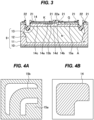
- Fig. 3 is a cross-sectional view showing a thyristor according to one aspect of the invention, and the same parts as in Fig. 1 are denoted by the same reference numerals and explanations thereof will be omitted.
- a first PN junction is formed between a fourth P-type semiconductor layer (P ++ ) 15b and a part (N ++ ) 14a of a bottom portion of a second N-type semiconductor layer (N + ) 14.
- a second PN junction is formed between a second P-type semiconductor layer (P + ) 13 and a first bottom portion (N + ) 14c of the second N-type semiconductor layer (N + ) 14 other than the part 14a of bottom portion.
- a third PN junction is formed between the second P-type semiconductor layer (P + ) 13 and a second bottom portion (N + ) 14d of the second N-type semiconductor layer (N + ) 14 other than the part 14a of bottom portion.
- the impurity concentration of the part (N ++ ) 14a of the bottom portion of the second N-type semiconductor layer (N + ) 14 is higher than that of each of the first and second bottom portions (N + ) 14c and 14d.
- the first PN junction is located closer to the gate electrode G side than the second PN junction
- the third PN junction is located closer to the gate electrode G side than the first PN junction.
- a first PN junction is formed between the fourth P-type semiconductor layer (second second base layer: P ++ ) 15b and the part (N ++ ) 14a of the bottom portion of the second N-type semiconductor layer (emitter layer: N + ) 14.
- a second PN junction is formed between the second P-type semiconductor layer (first base layer: P + ) 13 and the first bottom portion (N + ) 14c of the emitter layer (N + ) 14 other than the part 14a of the bottom portion.
- a third PN junction is formed between the first base layer (P + ) 13 and the second bottom portion (N + ) 14d of the emitter layer (N + ) 14 other than the part 14a of the bottom portion.
- the impurity concentration of the part (N ++ ) 14a of the bottom portion of the second N-type semiconductor layer (N + ) 14 is higher than that of each of the first and second bottom portions (N + ) 14c and 14d (see Figs. 3 and 5 ). This is because the manufacturing is based on a manufacturing method described in a third embodiment, which will be described later.
- reference numeral 15b in Fig. 5 corresponds to reference numeral 15b in Fig. 1 .
- the first PN junction is located closer to the gate electrode G side than the second PN junction (see Fig. 3 ). With such a structure, it is possible to adjust the gate characteristics.
- the fourth P-type semiconductor layer (second second base layer: P ++ ) 15b shown in Fig. 3 is disposed so as to cover the part 14a of the bottom portion of the second N-type semiconductor layer (emitter layer: N + ) 14 and so as not to cover the side portion 14b on the gate electrode G side.
- the second second base layer (P ++ ) 15b covers the part 14a of the bottom portion of the emitter layer (N + ) 14, it is possible to further desensitize the gate sensitivity of the thyristor. Therefore, even when this thyristor is used in a protection circuit for preventing an inrush current when an LED light is turned on, for example, it is possible to suppress an abnormal operation of the protection circuit for preventing an inrush current or the occurrence of malfunction due to minute noise. In addition to this, the critical off-voltage rise rate dv/dt resistance also increases.
- the thyristor manufacturing method of the above [9] includes: a step of forming a first P-type semiconductor layer (P + ) 11 below a first N-type semiconductor layer (N - ) 12 and forming a second P-type semiconductor layer (P + ) 13 on the first N-type semiconductor layer (N - ) 12; a step of forming a third P-type semiconductor layer (P ++ ) 15a and a fourth P-type semiconductor layer (P ++ ) 15b on a surface side of the second P-type semiconductor layer (P + ) 13; a step of forming a second N-type semiconductor layer (N + , N ++ ) 14 on the surface side of the second P-type semiconductor layer (P + ) 13 so as to partially overlap the fourth P-type semiconductor layer (P ++ ) 15b; and a step of forming a gate electrode G on the third P-type semiconductor layer (P ++ ) 15a and forming a cathode electrode K on
- the N-type semiconductor wafer 9 is prepared.
- isolation regions regions on both sides of the first N-type semiconductor layer (N - ) 12 are formed to partition the N-type semiconductor wafer 9 into a plurality of thyristor forming regions.
- Figs. 1 and 3 show one thyristor chip after the N-type semiconductor wafer 9 is cut by dicing.
- the N-type semiconductor wafer 9 includes the first N-type semiconductor layer (N - ) 12.
- the method for forming the isolation regions described above is to introduce P + -type impurities from both surfaces of the N-type semiconductor wafer 9 (a surface on the second N-type semiconductor layer (emitter layer: N + ) 14 side and a surface on the opposite side thereof) by using a deposition method and diffuse the P + -type impurities.
- P + -type impurities are introduced from both the surfaces of the N-type semiconductor wafer 9 described above by using a deposition method and diffused.
- the first P-type semiconductor layer (P + ) 11 is formed below the first N-type semiconductor layer (N - ) 12, and the second P-type semiconductor layer (first base layer: P + ) 13 is formed on the first N-type semiconductor layer (N - ) 12.
- the third P-type semiconductor layer (first second base layer: P ++ ) 15a and the fourth P-type semiconductor layer (second second base layer: P ++ ) 15b are formed on the surface side of the first base layer (P + ) 13, and a fifth P-type semiconductor layer (P ++ ) 10 is formed on the back side of the first P-type semiconductor layer (P + ) 11.
- N-type impurities are introduced into the first base layer (P + ) 13 by using a deposition method and diffused.
- the second N-type semiconductor layer (emitter layer: N + ) 14 is formed on the surface side of the first base layer (P + ) 13 so as to partially overlap the fourth P-type semiconductor layer (second second base layer: P ++ ) 15b (see Figs. 1, 2A, and 2B ).
- the above-described mask is removed, and a mask (not shown) is formed on the surface of the first base layer (P + ) 13.
- This mask has an opening in the second second base layer 15b except for the fourth P-type semiconductor layer (first second base layer: P ++ ) 15a side.
- N-type impurities are introduced into the first base layer (P + ) 13 by using a deposition method and diffused.
- the second N-type semiconductor layer (emitter layer: N ++ ) 14 is formed on the surface side of the second second base layer (P ++ ) 15b.
- the second N-type semiconductor layer (N + , N ++ ) 14 can be formed on the surface side of the first base layer (P + ) 13 so as to partially overlap the second second base layer 15b.
- the emitter layer (N ++ ) 14 on the surface side of the second second base layer (P ++ ) 15b becomes a region with excessive N-type impurities, and the depth of this region should not be larger than that of the second second base layer (P ++ ) 15b. That is, a boundary portion 14a between the emitter layer (N ++ ) 14 and the second second base layer (P ++ ) 15b is slightly shallower than the second second base layer (P ++ ) 15b (see Fig. 5 ) .
- the gate electrode G is formed on the third P-type semiconductor layer (first second base layer: P ++ ) 15a.
- This gate electrode is electrically connected to the first second base layer (P ++ ) 15a.
- first second base layer (P ++ ) 15a and the second second base layer (P ++ ) 15b can be formed on the surface side of the first base layer (P + ) 13 in the same process.
- the third P-type semiconductor layer (first second base layer: P ++ ) 15a has an impurity concentration higher than that of the second P-type semiconductor layer (P + ) 13.
- the fourth P-type semiconductor layer (second second base layer: P ++ ) 15b is formed below the cathode electrode K and has an impurity concentration higher than that of the second P-type semiconductor layer (P + ) 13.
- the third P-type semiconductor layer (first second base layer: P ++ ) 15a and the fourth P-type semiconductor layer (second second base layer: P ++ ) 15b are separated from each other by the second P-type semiconductor layer (first base layer: P + ) 13, and the first second base layer (P ++ ) 15a and the second N-type semiconductor layer (emitter layer: N + ) 14 are separated from each other by the first base layer (P + ) 13.
- the first second base layer (P ++ ) 15a which is connected to the gate electrode G and has an impurity concentration higher than that of the first base layer (P + ) 13, and the second second base layer (P ++ ) 15b, which is in contact with each of the first base layer (P + ) 13 and the emitter layer (N + ) 14, is disposed below the cathode electrode K, and has an impurity concentration higher than that of the first base layer (P + ) 13, are provided, it is possible to desensitize the gate sensitivity of the thyristor.
Landscapes
- Thyristors (AREA)
Abstract
Description
- This patent application claims the benefit and priority of
Japanese Patent Application No. 2021-171705 filed on October 20, 2021 - The present invention relates to a thyristor and a method for manufacturing the same.
- A conventional thyristor is used in a protection circuit to prevent an inrush current when an LED light is turned on.
- However, there are cases where gate sensitivity increases when changing to highly reliable passivation. In a protection circuit for preventing an inrush current using such a thyristor, there is a possibility that an abnormal operation may occur or malfunction may occur due to minute noise. For this reason, a thyristor with low gate sensitivity is required. A technique related to this is disclosed in
Japanese Patent Application Publication No. 2005-142518 - Various aspects of the present invention have an object to provide a thyristor with desensitized gate sensitivity and a method for manufacturing the same.
- Hereinafter, various aspects of the invention will be described.
- [1] A thyristor, including:
- a first P-type semiconductor layer;
- a first N-type semiconductor layer disposed in contact with the first P-type semiconductor layer;
- a second P-type semiconductor layer that is disposed in contact with the first N-type semiconductor layer and is separated from the first P-type semiconductor layer;
- a second N-type semiconductor layer disposed in contact with the second P-type semiconductor layer;
- a third P-type semiconductor layer that is disposed in contact with the second P-type semiconductor layer and has an impurity concentration higher than that of the second P-type semiconductor layer;
- a gate electrode electrically connected to the third P-type semiconductor layer;
- a cathode electrode electrically connected to the second N-type semiconductor layer; and
- a fourth P-type semiconductor layer that is in contact with each of the second P-type semiconductor layer and the second N-type semiconductor layer, is disposed below the cathode electrode, and has an impurity concentration higher than that of the second P-type semiconductor layer,
- wherein the third P-type semiconductor layer and the fourth P-type semiconductor layer are separated from each other by the second P-type semiconductor layer, and
- the third P-type semiconductor layer and the second N-type semiconductor layer are separated from each other by the second P-type semiconductor layer.
- [2] The thyristor according to [1] described above, in which the fourth P-type semiconductor layer is disposed on the third P-type semiconductor layer side in plan view.
- [3] The thyristor according to [1] or [2] described above, in which a first PN junction is formed between the fourth P-type semiconductor layer and a part of a bottom portion of the second N-type semiconductor layer, a second PN junction is formed between the second P-type semiconductor layer and a first bottom portion of the second N-type semiconductor layer other than the part of the bottom portion, and the first PN junction is located closer to the gate electrode side than the second PN junction in plan view.
- [4] The thyristor according to any one of [1] to [3] described above, in which the fourth P-type semiconductor layer is disposed so as to cover a part of a bottom portion of the second N-type semiconductor layer and a side portion of the second N-type semiconductor layer on the gate electrode side.
- [5] The thyristor according to [1] or [2] described above, in which a first PN junction is formed between the fourth P-type semiconductor layer and a part of a bottom portion of the second N-type semiconductor layer, a second PN junction is formed between the second P-type semiconductor layer and a first bottom portion of the second N-type semiconductor layer other than the part of the bottom portion, a third PN junction is formed between the second P-type semiconductor layer and a second bottom portion of the second N-type semiconductor layer other than the part of the bottom portion, an impurity concentration of the part of the bottom portion of the second N-type semiconductor layer is higher than that of each of the first and second bottom portions, and in plan view, the first PN junction is located closer to the gate electrode side than the second PN junction, and the third PN junction is located closer to the gate electrode side than the first PN junction.
- [6] The thyristor according to any one of [1], [2], and [5] described above, in which the fourth P-type semiconductor layer is disposed so as to cover a part of a bottom portion of the second N-type semiconductor layer and so as not to cover a side portion of the second N-type semiconductor layer on the gate electrode side.
- [7] The thyristor according to any one of [1] to [6] described above, in which an impurity concentration of the second N-type semiconductor layer is higher in a portion in contact with the fourth P-type semiconductor layer than in a portion not in contact with the fourth P-type semiconductor layer.
- [8] The thyristor according to any one of [1] to [7] described above, in which a ratio of an area of the fourth P-type semiconductor layer in contact with the second N-type semiconductor layer to an area of the second N-type semiconductor layer in plan view is 10% or more and 99% or less.
- [9] A thyristor manufacturing method, including:
- a step of forming a first P-type semiconductor layer below a first N-type semiconductor layer and forming a second P-type semiconductor layer on the first N-type semiconductor layer;
- a step of forming a third P-type semiconductor layer and a fourth P-type semiconductor layer on a surface side of the second P-type semiconductor layer;
- a step of forming a second N-type semiconductor layer on the surface side of the second P-type semiconductor layer so as to partially overlap the fourth P-type semiconductor layer; and
- a step of forming a gate electrode on the third P-type semiconductor layer and forming a cathode electrode on the second N-type semiconductor layer.
- [10] The thyristor manufacturing method according to [9] described above, in which the third P-type semiconductor layer has an impurity concentration higher than that of the second P-type semiconductor layer, the fourth P-type semiconductor layer is formed below the cathode electrode and has an impurity concentration higher than that of the second P-type semiconductor layer, the third P-type semiconductor layer and the fourth P-type semiconductor layer are separated from each other by the second P-type semiconductor layer, and the third P-type semiconductor layer and the second N-type semiconductor layer are separated from each other by the second P-type semiconductor layer.
- According to various aspects of the invention, it is possible to provide a thyristor with desensitized gate sensitivity and a method of manufacturing the same.
- Details will be described below.
- According to the thyristor of the above [1] of the invention, since the third P-type semiconductor layer, which is connected to the gate electrode and has an impurity concentration higher than that of the second P-type semiconductor layer, and the fourth P-type semiconductor layer, which is in contact with each of the second P-type semiconductor layer and the second N-type semiconductor layer, is disposed below the cathode electrode, and has an impurity concentration higher than that of the second P-type semiconductor layer, are provided, it is possible to desensitize the gate sensitivity of the thyristor.
- According to the thyristor of the above [2] of the invention, since the fourth P-type semiconductor layer is disposed on the third P-type semiconductor layer side in plan view, it is possible to further desensitize the gate sensitivity of the thyristor.
- According to the thyristor of the above [3] of the invention, since the first PN junction is located closer to the gate electrode side than the second PN junction in plan view, it is possible to further desensitize the gate sensitivity of the thyristor.
- According to the thyristor of the above [4] of the invention, since the fourth P-type semiconductor layer is disposed so as to cover a part of the bottom portion of the second N-type semiconductor layer and the side portion of the second N-type semiconductor layer on the gate electrode side, it is possible to further desensitize the gate sensitivity of the thyristor.
-
-
Fig. 1 is a cross-sectional view showing a thyristor according to one aspect of the invention; -
Fig. 2A is a plan view of a fourth P-type semiconductor layer (second second base layer: P++) 15b on the surface side of the thyristor shown inFig. 1, and Fig. 2B is a plan view showing a second N-type semiconductor layer (emitter layer: N+) 14 on the surface side of the thyristor shown inFig. 1 ; -
Fig. 3 is a cross-sectional view showing a thyristor according to one aspect of the invention; -
Fig. 4A is a plan view of a fourth P-type semiconductor layer (second second base layer: P++) 15b on the surface side of the thyristor shown inFig. 3, and Fig. 4B is a plan view showing a second N-type semiconductor layer (emitter layer: N+) 14 on the surface side of the thyristor shown inFig. 3 ; -
Fig. 5 is a partial cross-sectional view of the vicinity of the emitter layer (N+) 14 enlarged to explain the impurity concentration of the second N-type semiconductor layer (emitter layer: N+) 14 in the thyristor shown inFig. 1 ; and -
Fig. 6 is a diagram showing the dv/dt resistance of each thyristor sample of astructure 1 of the invention, astructure 2 of the invention, and a conventional structure. - Hereinafter, embodiments of the invention will be described in detail with reference to the drawings. However, the invention is not limited to the following description, and those skilled in the art will readily understand that various changes in forms and details can be made without departing from the spirit and scope of the invention. Therefore, the invention should not be construed as being limited to the descriptions of the embodiments below.
-
Fig. 1 is a cross-sectional view showing a thyristor according to one aspect of the invention.Fig. 2A is a plan view of a fourth P-type semiconductor layer (second second base layer: P++) 15b on the surface side of the thyristor shown inFig. 1, and Fig. 2B is a plan view showing a second N-type semiconductor layer (emitter layer: N+) 14 on the surface side of the thyristor shown inFig. 1 . In plan view in which the thyristor shown inFig. 1 is viewed from above, a plurality of layers overlap each other. Therefore, in order to makeFigs. 2A and 2B easier to understand, a case of a plan view of a specific layer is shown. - The thyristor of the above [1] according to one aspect of the invention includes: a first P-type semiconductor layer (P+) 11; a first N-type semiconductor layer (N-) 12 that is disposed in contact with the first P-type semiconductor layer (P+) 11 and is separated from the first P-type semiconductor layer (P+) 11; a second P-type semiconductor layer (P+) 13 disposed in contact with the first N-type semiconductor layer (N-) 12; a second N-type semiconductor layer (N+) 14 disposed in contact with the second P-type semiconductor layer 13; a third P-type semiconductor layer (P++) 15a that is disposed in contact with the second P-type semiconductor layer (P+) 13 and has an impurity concentration higher than that of the second P-type semiconductor layer (P+) 13; a gate electrode G electrically connected to the third P-type semiconductor layer (P++) 15a; a cathode electrode K electrically connected to the second N-type semiconductor layer (N+) 14; and a fourth P-type semiconductor layer (P++) 15b that is in contact with each of the second P-type semiconductor layer (P+) 13 and the second N-type semiconductor layer (N+) 14, is disposed below the cathode electrode K, and has an impurity concentration higher than that of the second P-type semiconductor layer (P+) 13. The third P-type semiconductor layer (P++) 15a and the fourth P-type semiconductor layer (P++) 15b are separated from each other by the second P-type semiconductor layer (P+) 13, and the third P-type semiconductor layer (P++) 15a and the second N-type semiconductor layer (N+) 14 are separated from each other by the second P-type semiconductor layer (P+) 13.
- Details will be described below.
- The thyristor shown in
Fig. 1 has an N-type semiconductor wafer 9, and the N-type semiconductor wafer 9 has the first P-type semiconductor layer (P+) 11. In addition,Figs. 1, 2A and 2B show one thyristor chip after the N-type semiconductor wafer 9 is cut by dicing. - As shown in
Fig. 1 , on the first P-type semiconductor layer (P+) 11, the first N-type semiconductor layer (N-) 12 is disposed so as to be in contact with the first P-type semiconductor layer (P+) 11. - On the first N-type semiconductor layer (N-) 12, the second P-type semiconductor layer (first base layer: P+) 13 is disposed so as to be in contact with the first N-type semiconductor layer (N-) 12. In addition, the concentrations of the first P-type semiconductor layer (P+) 11 and the second P-type semiconductor layer (P+) 13 may be the same, or either may be higher. In addition, the concentration range of each of the first P-type semiconductor layer (P+) 11 and the second P-type semiconductor layer (P+) 13 may be between 1 × 10¹⁶ atoms·cm-3 and 5 × 10¹⁸ atoms·cm-3.
- On the second P-type semiconductor layer (first base layer: P+) 13, the second N-type semiconductor layer (emitter layer: N+) 14 is disposed so as to be in contact with the second P-type semiconductor layer (first base layer: P+) 13. The planar shape of the emitter layer (N+) 14 is shown in
Fig. 2B . - In addition, on the second P-type semiconductor layer (first base layer: P+) 13, the third P-type semiconductor layer (first second base layer: P++) 15a is disposed so as to be in contact with the second P-type semiconductor layer (first base layer: P+) 13. The first second base layer (P++) 15a has a higher impurity concentration than the first base layer (P+) 13.
- A gate electrode G is electrically connected on the third P-type semiconductor layer (P++) 15a. The gate electrode G is preferably formed of Al.
- A cathode electrode K is electrically connected on the second N-type semiconductor layer (N+) 14. The cathode electrode K is preferably formed of Al.
- On the second P-type semiconductor layer (first base layer: P+) 13, the fourth P-type semiconductor layer (second second base layer: P++) 15b in contact with each of the
first base layer 13 and the second N-type semiconductor layer (emitter layer: N+) 14 is disposed. The second second base layer (P++) 15b is disposed below the cathode electrode K (seeFigs. 2A, 2B and3 ). In addition, the second second base layer (P++) 15 b has a higher impurity concentration than the first base layer (P+) 13. The planar shape of the second second base layer (P++) 15b is shown inFig. 2A . - The third P-type semiconductor layer (first second base layer: P++) 15a and the fourth P-type semiconductor layer (second second base layer: P++) 15b are separated from each other by the second P-type semiconductor layer (first base layer: P+) 13. In addition, the first second base layer (P++) 15a and the second N-type semiconductor layer (emitter layer: N+) 14 are separated from each other by the first base layer (P+) 13.
- In addition, as shown in
Fig. 1 , an SiO2 film 21 is formed on the emitter layer (N+) 14, the first base layer (P+) 13, and the first second base layer (P++) 15a. The cathode electrode K is formed on the emitter layer (N+) 14 and the SiO2 film 21. The gate electrode G is formed on the first second base layer (P++) 15a and the SiO2 film 21. In addition, aglass passivation film 22 is formed at each end of the first N-type semiconductor layer (N-) 12, the first base layer (P+) 13, the emitter layer (N+) 14, and the first second base layer (P++) 15a. In addition, theglass passivation film 22a is formed between the cathode electrode K and the gate electrode G. - According to the present embodiment, since the first second base layer (P++) 15a, which is connected to the gate electrode G and has an impurity concentration higher than that of the first base layer (P+) 13, and the second second base layer (P++) 15b, which is in contact with each of the first base layer (P+) 13 and the emitter layer (N+) 14, is disposed below the cathode electrode K, and has an impurity concentration higher than that of the first base layer (P+) 13, are provided, it is possible to desensitize the gate sensitivity of the thyristor. As a result, even when this thyristor is used in a protection circuit for preventing an inrush current when an LED light is turned on, for example, it is possible to suppress an abnormal operation of the protection circuit for preventing an inrush current or the occurrence of malfunction due to minute noise. In addition to this, the critical off-voltage rise rate dv/dt resistance also increases. Details thereof will be described later.
- In addition, by separating the first second base layer (P++) 15a and the second second base layer (P++) 15b from each other by the
first base layer 13, it is possible to further desensitize the gate sensitivity of the thyristor. - The reason why the above-described dv/dt resistance also increases is as follows.
- A thyristor requires a G (gate) current to turn on between A and K (between the anode A and the cathode K). When a positive voltage is applied to the anode A without turning on the thyristor, a depletion layer at a junction between the first N-type semiconductor layer (N-) 12 and the first base layer (P+) 13 shown in
Fig. 1 expands. This is the capacitance C of a condenser. Electrons move inside the thyristor to charge the capacitance C of the condenser. This charge current behaves the same as the G current. This current i is determined by the following equation.
- Therefore, since the current increases as the dv/dt value increases, the on operation (malfunction) is likely to occur even if the G current is not supplied.
- Therefore, by desensitizing the gate sensitivity, it is possible to realize a structure that has a high dv/dt value and is difficult to turn on even when a large charge current flows.
-
Fig. 6 is a diagram showing the dv/dt resistance of each thyristor sample of astructure 1 of the invention, astructure 2 of the invention, and a conventional structure. Thestructure 1 of the invention and thestructure 2 of the invention are thyristors having the structure shown inFig. 1 . Thestructure 2 of the invention is only different from thestructure 1 of the invention in that the ratio of the area of the second second base layer (P++) 15b shown inFig. 2A in contact with the emitter layer (N+) 14 to the area of the emitter layer (N+) 14 shown inFig. 2B in the thyristor according to one aspect of the invention shown inFig. 1 is larger than that in thestructure 1 of the invention, and the other points are the same. The conventional structure is different from thestructure 1 of the invention and thestructure 2 of the invention in that there is no second second base layer (P++) 15b shown inFig. 1 , and the other points are the same. - As shown in
Fig. 6 , it was confirmed that the presence of the second second base layer (P++) 15b increased the dv/dt resistance, and it was confirmed that the dv/dt resistance increased as the area of the second second base layer (P++) 15b in contact with the emitter layer (N+) 14 increased. - In addition, in plan view, the fourth P-type semiconductor layer (second second base layer: P++) 15b is disposed on the third P-type semiconductor layer (first second base layer: P++) 15a side (see
Figs. 1, 2A, 2B ,3, 4A and 4B ). In this manner, it is possible to further desensitize the gate sensitivity of the thyristor. - As shown in
Fig. 1 , a first PN junction is formed between the fourth P-type semiconductor layer (second second base layer: P++) 15b and apart 14a of a bottom portion of the second N-type semiconductor layer (emitter layer: N+) 14. In addition, a second PN junction is formed between the second P-type semiconductor layer (first base layer: P+) 13 and abottom portion 14c of the emitter layer (N+) 14 other than thepart 14a of the bottom portion. - In plan view, the first PN junction is located closer to the gate electrode G side than the second PN junction (see
Fig. 1 ). In this manner, it is possible to further desensitize the gate sensitivity of the thyristor. As a result, even when this thyristor is used in a protection circuit for preventing an inrush current when an LED light is turned on, for example, it is possible to suppress an abnormal operation of the protection circuit for preventing an inrush current or the occurrence of malfunction due to minute noise. In addition to this, the critical off-voltage rise rate dv/dt resistance also increases. - The fourth P-type semiconductor layer (second second base layer: P++) 15b is disposed so as to cover the
part 14a of the bottom portion of the second N-type semiconductor layer (emitter layer: N+) 14 and aside portion 14b on the gate electrode G side. In this manner, it is possible to further desensitize the gate sensitivity of the thyristor. Therefore, even when this thyristor is used in a protection circuit for preventing an inrush current when an LED light is turned on, for example, it is possible to suppress an abnormal operation of the protection circuit for preventing an inrush current or the occurrence of malfunction due to minute noise. In addition to this, the critical off-voltage rise rate dv/dt resistance also increases. -
Fig. 5 is a partial cross-sectional view of the vicinity of the emitter layer (N+) 14 enlarged to explain the impurity concentration of the second N-type semiconductor layer (emitter layer: N+) 14 in the thyristor shown inFig. 1 . - The impurity concentration of the second N-type semiconductor layer (emitter layer: N+) 14 is higher in a portion in contact with the fourth P-type semiconductor layer (second second base layer: P++) 15b than in a portion not in contact with the fourth P-type semiconductor layer (second second base layer: P++) 15b. Specifically, the impurity concentration of the second N-type semiconductor layer (N++) 14 located on the second second base layer (P++) 15b is higher than the impurity concentration of the second N-type semiconductor layer (N+) 14 below which the second second base layer (P++) 15b is not present. In addition, as shown in
Fig. 5 , this semiconductor device (thyristor) has a structure including the second N-type semiconductor layer (N++) 14, the second second base layer (P++) 15b, and an NPN-Tr at a junction between the second P-type semiconductor layer (first base layer: P+) 13 and the first N-type semiconductor layer (N-) 12. By adopting such a structure shown inFig. 5 , it is possible to change the NPN-Tr current gain. Therefore, after desensitizing the gate sensitivity, it becomes easier to adjust the sensitivity. - In plan view, as shown in
Figs. 2A and 2B , the ratio of the area of the fourth P-type semiconductor layer (second second base layer: P++) 15b in contact with the second N-type semiconductor layer (N+) 14 to the area of the second N-type semiconductor layer (emitter layer: N+) 14 is preferably 10% or more and 99% or less. In this manner, it is possible to further desensitize the gate sensitivity of the thyristor. As a result, even when this thyristor is used in a protection circuit for preventing an inrush current when an LED light is turned on, for example, it is possible to suppress an abnormal operation of the protection circuit for preventing an inrush current or the occurrence of malfunction due to minute noise. In addition to this, the critical off-voltage rise rate dv/dt resistance also increases. -
Fig. 3 is a cross-sectional view showing a thyristor according to one aspect of the invention, and the same parts as inFig. 1 are denoted by the same reference numerals and explanations thereof will be omitted. - A first PN junction is formed between a fourth P-type semiconductor layer (P++) 15b and a part (N++) 14a of a bottom portion of a second N-type semiconductor layer (N+) 14. In addition, a second PN junction is formed between a second P-type semiconductor layer (P+) 13 and a first bottom portion (N+) 14c of the second N-type semiconductor layer (N+) 14 other than the
part 14a of bottom portion. In addition, a third PN junction is formed between the second P-type semiconductor layer (P+) 13 and a second bottom portion (N+) 14d of the second N-type semiconductor layer (N+) 14 other than thepart 14a of bottom portion. The impurity concentration of the part (N++) 14a of the bottom portion of the second N-type semiconductor layer (N+) 14 is higher than that of each of the first and second bottom portions (N+) 14c and 14d. In plan view, the first PN junction is located closer to the gate electrode G side than the second PN junction, and the third PN junction is located closer to the gate electrode G side than the first PN junction. - Details will be described below.
- As shown in
Fig. 3 , a first PN junction is formed between the fourth P-type semiconductor layer (second second base layer: P++) 15b and the part (N++) 14a of the bottom portion of the second N-type semiconductor layer (emitter layer: N+) 14. In addition, a second PN junction is formed between the second P-type semiconductor layer (first base layer: P+) 13 and the first bottom portion (N+) 14c of the emitter layer (N+) 14 other than thepart 14a of the bottom portion. In addition, a third PN junction is formed between the first base layer (P+) 13 and the second bottom portion (N+) 14d of the emitter layer (N+) 14 other than thepart 14a of the bottom portion. - The impurity concentration of the part (N++) 14a of the bottom portion of the second N-type semiconductor layer (N+) 14 is higher than that of each of the first and second bottom portions (N+) 14c and 14d (see
Figs. 3 and5 ). This is because the manufacturing is based on a manufacturing method described in a third embodiment, which will be described later. In addition,reference numeral 15b inFig. 5 corresponds to reference numeral 15b inFig. 1 . - Also in the present embodiment, it is possible to obtain the same effects as in the first embodiment.
- In addition, in plan view, the first PN junction is located closer to the gate electrode G side than the second PN junction (see
Fig. 3 ). With such a structure, it is possible to adjust the gate characteristics. - The fourth P-type semiconductor layer (second second base layer: P++) 15b shown in
Fig. 3 is disposed so as to cover thepart 14a of the bottom portion of the second N-type semiconductor layer (emitter layer: N+) 14 and so as not to cover theside portion 14b on the gate electrode G side. - According to the present embodiment, since the second second base layer (P++) 15b covers the
part 14a of the bottom portion of the emitter layer (N+) 14, it is possible to further desensitize the gate sensitivity of the thyristor. Therefore, even when this thyristor is used in a protection circuit for preventing an inrush current when an LED light is turned on, for example, it is possible to suppress an abnormal operation of the protection circuit for preventing an inrush current or the occurrence of malfunction due to minute noise. In addition to this, the critical off-voltage rise rate dv/dt resistance also increases. - (Third embodiment: thyristor manufacturing method)
- The thyristor manufacturing method of the above [9] according to one aspect of the invention includes: a step of forming a first P-type semiconductor layer (P+) 11 below a first N-type semiconductor layer (N-) 12 and forming a second P-type semiconductor layer (P+) 13 on the first N-type semiconductor layer (N-) 12; a step of forming a third P-type semiconductor layer (P++) 15a and a fourth P-type semiconductor layer (P++) 15b on a surface side of the second P-type semiconductor layer (P+) 13; a step of forming a second N-type semiconductor layer (N+, N++) 14 on the surface side of the second P-type semiconductor layer (P+) 13 so as to partially overlap the fourth P-type semiconductor layer (P++) 15b; and a step of forming a gate electrode G on the third P-type semiconductor layer (P++) 15a and forming a cathode electrode K on the second N-type semiconductor layer (N+) 14.
- Details will be described below.
- First, as shown in
Fig. 1 , the N-type semiconductor wafer 9 is prepared. - Then, isolation regions (regions on both sides of the first N-type semiconductor layer (N-) 12) are formed to partition the N-
type semiconductor wafer 9 into a plurality of thyristor forming regions. In addition,Figs. 1 and3 show one thyristor chip after the N-type semiconductor wafer 9 is cut by dicing. In addition, the N-type semiconductor wafer 9 includes the first N-type semiconductor layer (N-) 12. - Here, the method for forming the isolation regions described above is to introduce P+-type impurities from both surfaces of the N-type semiconductor wafer 9 (a surface on the second N-type semiconductor layer (emitter layer: N+) 14 side and a surface on the opposite side thereof) by using a deposition method and diffuse the P+-type impurities.
- Then, P+-type impurities are introduced from both the surfaces of the N-
type semiconductor wafer 9 described above by using a deposition method and diffused. As a result, the first P-type semiconductor layer (P+) 11 is formed below the first N-type semiconductor layer (N-) 12, and the second P-type semiconductor layer (first base layer: P+) 13 is formed on the first N-type semiconductor layer (N-) 12. - Then, after forming a mask (not shown) on the second P-type semiconductor layer (P+) 13, P-type impurities are introduced into both the surfaces of the
semiconductor wafer 9 by using a deposition method and diffused. As a result, the third P-type semiconductor layer (first second base layer: P++) 15a and the fourth P-type semiconductor layer (second second base layer: P++) 15b are formed on the surface side of the first base layer (P+) 13, and a fifth P-type semiconductor layer (P++) 10 is formed on the back side of the first P-type semiconductor layer (P+) 11. - Then, after removing the above-described mask and forming a mask (not shown) on the surface of the second P-type semiconductor layer (first base layer: P+) 13, N-type impurities are introduced into the first base layer (P+) 13 by using a deposition method and diffused. As a result, the second N-type semiconductor layer (emitter layer: N+) 14 is formed on the surface side of the first base layer (P+) 13 so as to partially overlap the fourth P-type semiconductor layer (second second base layer: P++) 15b (see
Figs. 1, 2A, and 2B ). - Then, the above-described mask is removed, and a mask (not shown) is formed on the surface of the first base layer (P+) 13. This mask has an opening in the second
second base layer 15b except for the fourth P-type semiconductor layer (first second base layer: P++) 15a side. Then, N-type impurities are introduced into the first base layer (P+) 13 by using a deposition method and diffused. As a result, as shown inFig. 5 , the second N-type semiconductor layer (emitter layer: N++) 14 is formed on the surface side of the second second base layer (P++) 15b. In this manner, the second N-type semiconductor layer (N+, N++) 14 can be formed on the surface side of the first base layer (P+) 13 so as to partially overlap the secondsecond base layer 15b. After forming the second second base layer (P++) 15b as described above, in order to make the surface side of the second second base layer (P++) 15b into the opposite conductivity type emitter layer (N++) 14, the emitter layer (N++) 14 on the surface side of the second second base layer (P++) 15b becomes a region with excessive N-type impurities, and the depth of this region should not be larger than that of the second second base layer (P++) 15b. That is, aboundary portion 14a between the emitter layer (N++) 14 and the second second base layer (P++) 15b is slightly shallower than the second second base layer (P++) 15b (seeFig. 5 ) . - Then, the above-described mask is removed, and the gate electrode G is formed on the third P-type semiconductor layer (first second base layer: P++) 15a. This gate electrode is electrically connected to the first second base layer (P++) 15a.
- Also in the present embodiment, it is possible to obtain the same effects as in the first embodiment.
- In addition, according to the present embodiment, the first second base layer (P++) 15a and the second second base layer (P++) 15b can be formed on the surface side of the first base layer (P+) 13 in the same process.
- In addition, the third P-type semiconductor layer (first second base layer: P++) 15a has an impurity concentration higher than that of the second P-type semiconductor layer (P+) 13.
- In addition, the fourth P-type semiconductor layer (second second base layer: P++) 15b is formed below the cathode electrode K and has an impurity concentration higher than that of the second P-type semiconductor layer (P+) 13.
- In addition, the third P-type semiconductor layer (first second base layer: P++) 15a and the fourth P-type semiconductor layer (second second base layer: P++) 15b are separated from each other by the second P-type semiconductor layer (first base layer: P+) 13, and the first second base layer (P++) 15a and the second N-type semiconductor layer (emitter layer: N+) 14 are separated from each other by the first base layer (P+) 13.
- According to the present embodiment, since the first second base layer (P++) 15a, which is connected to the gate electrode G and has an impurity concentration higher than that of the first base layer (P+) 13, and the second second base layer (P++) 15b, which is in contact with each of the first base layer (P+) 13 and the emitter layer (N+) 14, is disposed below the cathode electrode K, and has an impurity concentration higher than that of the first base layer (P+) 13, are provided, it is possible to desensitize the gate sensitivity of the thyristor.
-
- 11 FIRST P-TYPE SEMICONDUCTOR LAYER (P+)
- 12 FIRST N-TYPE SEMICONDUCTOR LAYER (N-)
- 13 SECOND P-TYPE SEMICONDUCTOR LAYER (FIRST BASE LAYER: P+)
- 14 SECOND N-TYPE SEMICONDUCTOR LAYER (EMITTER LAYER: N+)
- 14a PART (N++) OF BOTTOM PORTION OF SECOND N-TYPE SEMICONDUCTOR LAYER (N+)
- 14b SIDE PORTION ON GATE ELECTRODE SIDE
- 14c FIRST BOTTOM PORTION (N+) OF SECOND N-TYPE SEMICONDUCTOR LAYER (N+) OTHER THAN PART OF BOTTOM PORTION
- 14d SECOND BOTTOM PORTION (N+) OF SECOND N-TYPE SEMICONDUCTOR LAYER OTHER THAN PART OF BOTTOM PORTION
- 15a THIRD P-TYPE SEMICONDUCTOR LAYER (FIRST SECOND BASE LAYER: P++)
- 15b FOURTH P-TYPE SEMICONDUCTOR LAYER (SECOND SECOND BASE LAYER: P++)
- G GATE ELECTRODE
- K CATHODE ELECTRODE
Claims (10)
- A thyristor, comprising:a first P-type semiconductor layer;a first N-type semiconductor layer disposed in contact with the first P-type semiconductor layer;a second P-type semiconductor layer that is disposed in contact with the first N-type semiconductor layer and is separated from the first P-type semiconductor layer;a second N-type semiconductor layer disposed in contact with the second P-type semiconductor layer;a third P-type semiconductor layer that is disposed in contact with the second P-type semiconductor layer and has an impurity concentration higher than that of the second P-type semiconductor layer;a gate electrode electrically connected to the third P-type semiconductor layer;a cathode electrode electrically connected to the second N-type semiconductor layer; anda fourth P-type semiconductor layer that is in contact with each of the second P-type semiconductor layer and the second N-type semiconductor layer, is disposed below the cathode electrode, and has an impurity concentration higher than that of the second P-type semiconductor layer,wherein the third P-type semiconductor layer and the fourth P-type semiconductor layer are separated from each other by the second P-type semiconductor layer, andthe third P-type semiconductor layer and the second N-type semiconductor layer are separated from each other by the second P-type semiconductor layer.
- The thyristor according to claim 1,
wherein the fourth P-type semiconductor layer is disposed on the third P-type semiconductor layer side in plan view. - The thyristor according to claim 1 or 2,wherein a first PN junction is formed between the fourth P-type semiconductor layer and a part of a bottom portion of the second N-type semiconductor layer,a second PN junction is formed between the second P-type semiconductor layer and a first bottom portion of the second N-type semiconductor layer other than the part of the bottom portion, andthe first PN junction is located closer to the gate electrode side than the second PN junction in plan view.
- The thyristor according to claim 1 or 2,
wherein the fourth P-type semiconductor layer is disposed so as to cover a part of a bottom portion of the second N-type semiconductor layer and a side portion of the second N-type semiconductor layer on the gate electrode side. - The thyristor according to claim 1 or 2,wherein a first PN junction is formed between the fourth P-type semiconductor layer and a part of a bottom portion of the second N-type semiconductor layer,a second PN junction is formed between the second P-type semiconductor layer and a first bottom portion of the second N-type semiconductor layer other than the part of the bottom portion,a third PN junction is formed between the second P-type semiconductor layer and a second bottom portion of the second N-type semiconductor layer other than the part of the bottom portion,an impurity concentration of the part of the bottom portion of the second N-type semiconductor layer is higher than that of each of the first and second bottom portions, andin plan view, the first PN junction is located closer to the gate electrode side than the second PN junction, and the third PN junction is located closer to the gate electrode side than the first PN junction.
- The thyristor according to claim 1 or 2,
wherein the fourth P-type semiconductor layer is disposed so as to cover a part of a bottom portion of the second N-type semiconductor layer and so as not to cover a side portion of the second N-type semiconductor layer on the gate electrode side. - The thyristor according to claim 1 or 2,
wherein an impurity concentration of the second N-type semiconductor layer is higher in a portion in contact with the fourth P-type semiconductor layer than in a portion not in contact with the fourth P-type semiconductor layer. - The thyristor according to claim 1 or 2,
wherein a ratio of an area of the fourth P-type semiconductor layer in contact with the second N-type semiconductor layer to an area of the second N-type semiconductor layer in plan view is 10% or more and 99% or less. - A thyristor manufacturing method, comprising:a step of forming a first P-type semiconductor layer below a first N-type semiconductor layer and forming a second P-type semiconductor layer on the first N-type semiconductor layer;a step of forming a third P-type semiconductor layer and a fourth P-type semiconductor layer on a surface side of the second P-type semiconductor layer;a step of forming a second N-type semiconductor layer on the surface side of the second P-type semiconductor layer so as to partially overlap the fourth P-type semiconductor layer; anda step of forming a gate electrode on the third P-type semiconductor layer and forming a cathode electrode on the second N-type semiconductor layer.
- The thyristor manufacturing method according to claim 9,wherein the third P-type semiconductor layer has an impurity concentration higher than that of the second P-type semiconductor layer,the fourth P-type semiconductor layer is formed below the cathode electrode and has an impurity concentration higher than that of the second P-type semiconductor layer,the third P-type semiconductor layer and the fourth P-type semiconductor layer are separated from each other by the second P-type semiconductor layer, andthe third P-type semiconductor layer and the second N-type semiconductor layer are separated from each other by the second P-type semiconductor layer.
Applications Claiming Priority (2)
| Application Number | Priority Date | Filing Date | Title |
|---|---|---|---|
| JP2021171705 | 2021-10-20 | ||
| PCT/JP2022/036134 WO2023067997A1 (en) | 2021-10-20 | 2022-09-28 | Thyristor and method for manufacturing same |
Publications (2)
| Publication Number | Publication Date |
|---|---|
| EP4421876A1 true EP4421876A1 (en) | 2024-08-28 |
| EP4421876A4 EP4421876A4 (en) | 2025-01-15 |
Family
ID=86059119
Family Applications (1)
| Application Number | Title | Priority Date | Filing Date |
|---|---|---|---|
| EP22877674.6A Pending EP4421876A4 (en) | 2021-10-20 | 2022-09-28 | THYRISTOR AND ITS MANUFACTURING PROCESS |
Country Status (6)
| Country | Link |
|---|---|
| US (1) | US20240006510A1 (en) |
| EP (1) | EP4421876A4 (en) |
| JP (1) | JPWO2023067997A1 (en) |
| CN (1) | CN116391258A (en) |
| TW (1) | TWI832486B (en) |
| WO (1) | WO2023067997A1 (en) |
Family Cites Families (16)
| Publication number | Priority date | Publication date | Assignee | Title |
|---|---|---|---|---|
| JPS5510984B2 (en) * | 1972-11-29 | 1980-03-21 | ||
| JPS5595363A (en) * | 1979-01-11 | 1980-07-19 | Nec Corp | Thyristor |
| JPS5679470A (en) * | 1979-11-30 | 1981-06-30 | Nec Corp | Semiconductor device |
| JPS6252967A (en) * | 1985-08-31 | 1987-03-07 | Fuji Electric Co Ltd | GTO thyristor |
| US5319222A (en) * | 1992-04-29 | 1994-06-07 | North Carolina State University | MOS gated thyristor having on-state current saturation capability |
| FR2754392B1 (en) * | 1996-10-04 | 1999-04-30 | Centre Nat Rech Scient | NORMALLY PASSING THYRISTOR DUAL LOCKABLE BY A PULSE APPLIED ON THE TRIGGER |
| JP3977518B2 (en) * | 1998-07-14 | 2007-09-19 | 関西電力株式会社 | Static induction semiconductor device |
| JP2005142518A (en) | 2003-11-07 | 2005-06-02 | Success International Kk | Planar thyristor manufacturing method |
| JP5552249B2 (en) * | 2009-03-27 | 2014-07-16 | 新電元工業株式会社 | 3-terminal thyristor |
| JP2014123633A (en) * | 2012-12-20 | 2014-07-03 | Renesas Electronics Corp | Semiconductor device |
| CN103219372B (en) * | 2013-04-10 | 2015-10-28 | 株洲南车时代电气股份有限公司 | A kind of thyristor gate cathode junction and there is the door pole stream-exchanging thyristor of this structure |
| FR3039014B1 (en) * | 2015-07-13 | 2019-06-14 | Stmicroelectronics (Tours) Sas | TELEPHONE LINE PROTECTION AGAINST OVERVOLTAGES |
| JP6157043B1 (en) * | 2015-09-18 | 2017-07-05 | 新電元工業株式会社 | Semiconductor device and manufacturing method of semiconductor device |
| JP7051520B2 (en) * | 2018-03-22 | 2022-04-11 | 新電元工業株式会社 | Manufacturing method of semiconductor device and semiconductor device |
| EP4006989B1 (en) * | 2020-11-25 | 2024-05-15 | Hitachi Energy Ltd | Bidirectional thyristor device with asymmetric characteristics |
| JP2024095363A (en) * | 2022-12-28 | 2024-07-10 | 国立大学法人東北大学 | Receiver, frequency spectrum regeneration method, and frequency spectrum regeneration program |
-
2022
- 2022-09-28 WO PCT/JP2022/036134 patent/WO2023067997A1/en not_active Ceased
- 2022-09-28 US US18/251,906 patent/US20240006510A1/en active Pending
- 2022-09-28 JP JP2023525987A patent/JPWO2023067997A1/ja active Pending
- 2022-09-28 CN CN202280006881.0A patent/CN116391258A/en active Pending
- 2022-09-28 EP EP22877674.6A patent/EP4421876A4/en active Pending
- 2022-10-13 TW TW111138734A patent/TWI832486B/en active
Also Published As
| Publication number | Publication date |
|---|---|
| EP4421876A4 (en) | 2025-01-15 |
| TW202318676A (en) | 2023-05-01 |
| JPWO2023067997A1 (en) | 2023-04-27 |
| US20240006510A1 (en) | 2024-01-04 |
| TWI832486B (en) | 2024-02-11 |
| CN116391258A (en) | 2023-07-04 |
| WO2023067997A1 (en) | 2023-04-27 |
Similar Documents
| Publication | Publication Date | Title |
|---|---|---|
| JP4156717B2 (en) | Semiconductor device | |
| KR0128673B1 (en) | Semiconductor device and manufacturing method thereof | |
| US20240055516A1 (en) | Semiconductor device | |
| US11239358B2 (en) | Semiconductor structure with isolation structures in doped region and fabrication method thereof | |
| US20130093057A1 (en) | Semiconductor device | |
| US11114572B2 (en) | Semiconductor device and method for manufacturing semiconductor device | |
| KR900000062B1 (en) | Leakage current improved type mis fet semiconductor device | |
| US10418479B2 (en) | Semiconductor device and method of manufacturing semiconductor device | |
| US20240006510A1 (en) | Thyristor and method for manufacturing the same | |
| US11569379B2 (en) | Semiconductor device and semiconductor device manufacturing method | |
| US11217541B2 (en) | Transistors with electrically active chip seal ring and methods of manufacture | |
| US7026705B2 (en) | Semiconductor device with surge protection circuit capable of preventing current leakage | |
| JP2006156963A (en) | Semiconductor structures that isolate integrated circuits of various operating voltages | |
| US5567978A (en) | High voltage, junction isolation semiconductor device having dual conductivity tape buried regions and its process of manufacture | |
| US20220328617A1 (en) | Field effect transistor and method for manufacturing the same | |
| US20220238727A1 (en) | Zener diode and manufacturing method thereof | |
| JPH04291952A (en) | Semiconductor device | |
| KR101121702B1 (en) | Semiconductor device | |
| KR100625362B1 (en) | Transient Voltage Suppression Element and Manufacturing Method Thereof | |
| JPS6035558A (en) | Semiconductor integrated circuit device and manufacture thereof | |
| US11791220B2 (en) | Semiconductor device and semiconductor device fabrication method | |
| US20060278889A1 (en) | Power rectifier and manufacturing method thereof | |
| JPH02170469A (en) | Semiconductor device | |
| KR19980030445A (en) | Antistatic device | |
| KR100464383B1 (en) | Semiconductor device using trench isolation |
Legal Events
| Date | Code | Title | Description |
|---|---|---|---|
| STAA | Information on the status of an ep patent application or granted ep patent |
Free format text: STATUS: UNKNOWN |
|
| STAA | Information on the status of an ep patent application or granted ep patent |
Free format text: STATUS: THE INTERNATIONAL PUBLICATION HAS BEEN MADE |
|
| PUAI | Public reference made under article 153(3) epc to a published international application that has entered the european phase |
Free format text: ORIGINAL CODE: 0009012 |
|
| STAA | Information on the status of an ep patent application or granted ep patent |
Free format text: STATUS: REQUEST FOR EXAMINATION WAS MADE |
|
| 17P | Request for examination filed |
Effective date: 20230413 |
|
| AK | Designated contracting states |
Kind code of ref document: A1 Designated state(s): AL AT BE BG CH CY CZ DE DK EE ES FI FR GB GR HR HU IE IS IT LI LT LU LV MC MK MT NL NO PL PT RO RS SE SI SK SM TR |
|
| REG | Reference to a national code |
Ref country code: DE Ref legal event code: R079 Free format text: PREVIOUS MAIN CLASS: H01L0029740000 Ipc: H01L0029744000 |
|
| A4 | Supplementary search report drawn up and despatched |
Effective date: 20241216 |
|
| RIC1 | Information provided on ipc code assigned before grant |
Ipc: H01L 29/10 20060101ALI20241210BHEP Ipc: H01L 29/08 20060101ALI20241210BHEP Ipc: H01L 29/06 20060101ALI20241210BHEP Ipc: H01L 29/744 20060101AFI20241210BHEP |
|
| DAV | Request for validation of the european patent (deleted) | ||
| DAX | Request for extension of the european patent (deleted) |