EP4421868A1 - Semiconductor module arrangement - Google Patents
Semiconductor module arrangement Download PDFInfo
- Publication number
- EP4421868A1 EP4421868A1 EP23158107.5A EP23158107A EP4421868A1 EP 4421868 A1 EP4421868 A1 EP 4421868A1 EP 23158107 A EP23158107 A EP 23158107A EP 4421868 A1 EP4421868 A1 EP 4421868A1
- Authority
- EP
- European Patent Office
- Prior art keywords
- layer
- metallization layer
- additional
- dielectric insulation
- electrode
- Prior art date
- Legal status (The legal status is an assumption and is not a legal conclusion. Google has not performed a legal analysis and makes no representation as to the accuracy of the status listed.)
- Granted
Links
Images



Classifications
-
- H—ELECTRICITY
- H10—SEMICONDUCTOR DEVICES; ELECTRIC SOLID-STATE DEVICES NOT OTHERWISE PROVIDED FOR
- H10W—GENERIC PACKAGES, INTERCONNECTIONS, CONNECTORS OR OTHER CONSTRUCTIONAL DETAILS OF DEVICES COVERED BY CLASS H10
- H10W76/00—Containers; Fillings or auxiliary members therefor; Seals
- H10W76/10—Containers or parts thereof
- H10W76/12—Containers or parts thereof characterised by their shape
- H10W76/15—Containers comprising an insulating or insulated base
-
- H—ELECTRICITY
- H10—SEMICONDUCTOR DEVICES; ELECTRIC SOLID-STATE DEVICES NOT OTHERWISE PROVIDED FOR
- H10W—GENERIC PACKAGES, INTERCONNECTIONS, CONNECTORS OR OTHER CONSTRUCTIONAL DETAILS OF DEVICES COVERED BY CLASS H10
- H10W40/00—Arrangements for thermal protection or thermal control
- H10W40/20—Arrangements for cooling
- H10W40/25—Arrangements for cooling characterised by their materials
- H10W40/255—Arrangements for cooling characterised by their materials having a laminate or multilayered structure, e.g. direct bond copper [DBC] ceramic substrates
-
- H—ELECTRICITY
- H10—SEMICONDUCTOR DEVICES; ELECTRIC SOLID-STATE DEVICES NOT OTHERWISE PROVIDED FOR
- H10W—GENERIC PACKAGES, INTERCONNECTIONS, CONNECTORS OR OTHER CONSTRUCTIONAL DETAILS OF DEVICES COVERED BY CLASS H10
- H10W70/00—Package substrates; Interposers; Redistribution layers [RDL]
- H10W70/60—Insulating or insulated package substrates; Interposers; Redistribution layers
- H10W70/611—Insulating or insulated package substrates; Interposers; Redistribution layers for connecting multiple chips together
-
- H—ELECTRICITY
- H10—SEMICONDUCTOR DEVICES; ELECTRIC SOLID-STATE DEVICES NOT OTHERWISE PROVIDED FOR
- H10W—GENERIC PACKAGES, INTERCONNECTIONS, CONNECTORS OR OTHER CONSTRUCTIONAL DETAILS OF DEVICES COVERED BY CLASS H10
- H10W76/00—Containers; Fillings or auxiliary members therefor; Seals
- H10W76/40—Fillings or auxiliary members in containers, e.g. centering rings
- H10W76/42—Fillings
- H10W76/47—Solid or gel fillings
-
- H—ELECTRICITY
- H10—SEMICONDUCTOR DEVICES; ELECTRIC SOLID-STATE DEVICES NOT OTHERWISE PROVIDED FOR
- H10W—GENERIC PACKAGES, INTERCONNECTIONS, CONNECTORS OR OTHER CONSTRUCTIONAL DETAILS OF DEVICES COVERED BY CLASS H10
- H10W90/00—Package configurations
-
- H—ELECTRICITY
- H10—SEMICONDUCTOR DEVICES; ELECTRIC SOLID-STATE DEVICES NOT OTHERWISE PROVIDED FOR
- H10W—GENERIC PACKAGES, INTERCONNECTIONS, CONNECTORS OR OTHER CONSTRUCTIONAL DETAILS OF DEVICES COVERED BY CLASS H10
- H10W90/00—Package configurations
- H10W90/401—Package configurations characterised by multiple insulating or insulated package substrates, interposers or RDLs
-
- H—ELECTRICITY
- H10—SEMICONDUCTOR DEVICES; ELECTRIC SOLID-STATE DEVICES NOT OTHERWISE PROVIDED FOR
- H10W—GENERIC PACKAGES, INTERCONNECTIONS, CONNECTORS OR OTHER CONSTRUCTIONAL DETAILS OF DEVICES COVERED BY CLASS H10
- H10W72/00—Interconnections or connectors in packages
- H10W72/071—Connecting or disconnecting
- H10W72/075—Connecting or disconnecting of bond wires
- H10W72/07551—Connecting or disconnecting of bond wires characterised by changes in properties of the bond wires during the connecting
- H10W72/07554—Connecting or disconnecting of bond wires characterised by changes in properties of the bond wires during the connecting changes in dispositions
-
- H—ELECTRICITY
- H10—SEMICONDUCTOR DEVICES; ELECTRIC SOLID-STATE DEVICES NOT OTHERWISE PROVIDED FOR
- H10W—GENERIC PACKAGES, INTERCONNECTIONS, CONNECTORS OR OTHER CONSTRUCTIONAL DETAILS OF DEVICES COVERED BY CLASS H10
- H10W72/00—Interconnections or connectors in packages
- H10W72/50—Bond wires
- H10W72/541—Dispositions of bond wires
- H10W72/547—Dispositions of multiple bond wires
-
- H—ELECTRICITY
- H10—SEMICONDUCTOR DEVICES; ELECTRIC SOLID-STATE DEVICES NOT OTHERWISE PROVIDED FOR
- H10W—GENERIC PACKAGES, INTERCONNECTIONS, CONNECTORS OR OTHER CONSTRUCTIONAL DETAILS OF DEVICES COVERED BY CLASS H10
- H10W72/00—Interconnections or connectors in packages
- H10W72/851—Dispositions of multiple connectors or interconnections
- H10W72/874—On different surfaces
- H10W72/884—Die-attach connectors and bond wires
-
- H—ELECTRICITY
- H10—SEMICONDUCTOR DEVICES; ELECTRIC SOLID-STATE DEVICES NOT OTHERWISE PROVIDED FOR
- H10W—GENERIC PACKAGES, INTERCONNECTIONS, CONNECTORS OR OTHER CONSTRUCTIONAL DETAILS OF DEVICES COVERED BY CLASS H10
- H10W90/00—Package configurations
- H10W90/701—Package configurations characterised by the relative positions of pads or connectors relative to package parts
-
- H—ELECTRICITY
- H10—SEMICONDUCTOR DEVICES; ELECTRIC SOLID-STATE DEVICES NOT OTHERWISE PROVIDED FOR
- H10W—GENERIC PACKAGES, INTERCONNECTIONS, CONNECTORS OR OTHER CONSTRUCTIONAL DETAILS OF DEVICES COVERED BY CLASS H10
- H10W90/00—Package configurations
- H10W90/701—Package configurations characterised by the relative positions of pads or connectors relative to package parts
- H10W90/731—Package configurations characterised by the relative positions of pads or connectors relative to package parts of die-attach connectors
- H10W90/734—Package configurations characterised by the relative positions of pads or connectors relative to package parts of die-attach connectors between a chip and a stacked insulating package substrate, interposer or RDL
-
- H—ELECTRICITY
- H10—SEMICONDUCTOR DEVICES; ELECTRIC SOLID-STATE DEVICES NOT OTHERWISE PROVIDED FOR
- H10W—GENERIC PACKAGES, INTERCONNECTIONS, CONNECTORS OR OTHER CONSTRUCTIONAL DETAILS OF DEVICES COVERED BY CLASS H10
- H10W90/00—Package configurations
- H10W90/701—Package configurations characterised by the relative positions of pads or connectors relative to package parts
- H10W90/751—Package configurations characterised by the relative positions of pads or connectors relative to package parts of bond wires
- H10W90/753—Package configurations characterised by the relative positions of pads or connectors relative to package parts of bond wires between laterally-adjacent chips
-
- H—ELECTRICITY
- H10—SEMICONDUCTOR DEVICES; ELECTRIC SOLID-STATE DEVICES NOT OTHERWISE PROVIDED FOR
- H10W—GENERIC PACKAGES, INTERCONNECTIONS, CONNECTORS OR OTHER CONSTRUCTIONAL DETAILS OF DEVICES COVERED BY CLASS H10
- H10W90/00—Package configurations
- H10W90/701—Package configurations characterised by the relative positions of pads or connectors relative to package parts
- H10W90/751—Package configurations characterised by the relative positions of pads or connectors relative to package parts of bond wires
- H10W90/754—Package configurations characterised by the relative positions of pads or connectors relative to package parts of bond wires between a chip and a stacked insulating package substrate, interposer or RDL
Definitions
- the instant disclosure relates to a semiconductor module arrangement, in particular to a power semiconductor module arrangement comprising at least one controllable semiconductor element.
- Power semiconductor module arrangements often include at least one semiconductor substrate arranged in a housing.
- a semiconductor arrangement including a plurality of controllable semiconductor elements e.g., IGBTs, MOSFETs, HEMTs, etc.
- Each substrate usually comprises a substrate layer (e.g., a ceramic layer), a first metallization layer deposited on a first side of the substrate layer, and, optionally, a second metallization layer deposited on a second side of the substrate layer.
- the controllable semiconductor elements are mounted, for example, on the first metallization layer.
- the second metallization layer may optionally be attached to a base plate.
- the layout of the semiconductor arrangement should be chosen to minimize the required size of the at least one substrate while, at the same time, heat that is generated during operation of the power semiconductor module arrangement is efficiently dissipated away from the controllable semiconductor elements and the substrate.
- a power semiconductor module arrangement includes a substrate including a dielectric insulation layer and a first metallization layer arranged on a first side of the dielectric insulation layer, wherein the first metallization layer includes a plurality of different sections that are separate and distinct from each other, and a plurality of semiconductor bodies arranged on the first metallization layer, wherein a first electrode of each of the plurality of semiconductor bodies is electrically coupled to a first section of the first metallization layer, a second electrode of each of the plurality of semiconductor bodies is electrically coupled to a second section of the first metallization layer, a third electrode of each of the plurality of semiconductor bodies is electrically coupled to an additional metallization layer by means of one or more electrical connection elements, the additional metallization layer is arranged distant from and in parallel to the first metallization layer, and the additional metallization layer is arranged on an additional dielectric insulation layer, wherein the additional dielectric insulation layer is arranged in parallel to and distant from the dielectric insulation layer, and wherein the additional dielectric insulation layer is arranged between the
- An electrical line or electrical connection as described herein may be a single electrically conductive element, or include at least two individual electrically conductive elements connected in series and/or parallel. Electrical lines and electrical connections may include metal and/or semiconductor material, and may be permanently electrically conductive (i.e., non-switchable).
- a semiconductor body as described herein may be made from (doped) semiconductor material and may be a semiconductor chip or be included in a semiconductor chip. A semiconductor body has electrically connecting pads and includes at least one semiconductor element with electrodes.
- the power semiconductor module arrangement 100 includes a housing 7 and a substrate 10.
- the substrate 10 includes a dielectric insulation layer 11, a (structured) first metallization layer 111 attached to the dielectric insulation layer 11, and a (structured) second metallization layer 112 attached to the dielectric insulation layer 11.
- the dielectric insulation layer 11 is disposed between the first and second metallization layers 111, 112.
- Each of the first and second metallization layers 111, 112 may consist of or include one of the following materials: copper; a copper alloy; aluminum; an aluminum alloy; any other metal or alloy that remains solid during the operation of the power semiconductor module arrangement.
- the substrate 10 may be a ceramic substrate, that is, a substrate in which the dielectric insulation layer 11 is a ceramic, e.g., a thin ceramic layer.
- the ceramic may consist of or include one of the following materials: aluminum oxide; aluminum nitride; zirconium oxide; silicon nitride; boron nitride; or any other dielectric ceramic.
- the dielectric insulation layer 11 may consist of or include one of the following materials: Al 2 O 3 , AlN, SiC, BeO or Si 3 N 4 .
- the substrate 10 may, e.g., be a Direct Copper Bonding (DCB) substrate, a Direct Aluminum Bonding (DAB) substrate, or an Active Metal Brazing (AMB) substrate.
- the substrate 10 may be an Insulated Metal Substrate (IMS).
- An Insulated Metal Substrate generally comprises a dielectric insulation layer 11 comprising (filled) materials such as epoxy resin or polyimide, for example.
- the material of the dielectric insulation layer 11 may be filled with ceramic particles, for example. Such particles may comprise, e.g., SiO 2 , Al 2 O 3 , AlN, or BN and may have a diameter of between about 1 ⁇ m and about 50 ⁇ m.
- the substrate 10 may also be a conventional printed circuit board (PCB) having a non-ceramic dielectric insulation layer 11.
- a non-ceramic dielectric insulation layer 11 may consist of or include a cured resin.
- the substrate 10 is arranged in a housing 7.
- the substrate 10 is arranged on a base plate 12 which forms a ground surface of the housing 7, while the housing 7 itself solely comprises sidewalls and a cover.
- the housing 7 further comprises a ground surface and the substrate 10 and the base plate 12 be arranged inside the housing 7.
- more than one substrate 10 is arranged on a single base plate 12 or on the ground surface of a housing 7. It is also possible that the substrate 10 itself forms a ground surface of the housing 7.
- One or more semiconductor bodies 20 may be arranged on the at least one substrate 10.
- Each of the semiconductor bodies 20 arranged on the at least one substrate 10 may include a diode, an IGBT (Insulated-Gate Bipolar Transistor), a MOSFET (Metal-Oxide-Semiconductor Field-Effect Transistor), a JFET (Junction Field-Effect Transistor), a HEMT (High-Electron-Mobility Transistor), and/or any other suitable semiconductor element.
- IGBT Insulated-Gate Bipolar Transistor
- MOSFET Metal-Oxide-Semiconductor Field-Effect Transistor
- JFET Joint Field-Effect Transistor
- HEMT High-Electron-Mobility Transistor
- the one or more semiconductor bodies 20 may form a semiconductor arrangement on the substrate 10.
- the second metallization layer 112 of the substrate 10 in Figure 1 is a continuous layer.
- the first metallization layer 111 is a structured layer in the example illustrated in Figure 1 .
- "Structured layer” means that the first metallization layer 111 is not a continuous layer, but includes recesses between different sections of the layer. Such recesses are schematically illustrated in Figure 1 .
- the first metallization layer 111 in this example includes three different sections. This, however, is only an example. Any other number of sections is possible. Different semiconductor bodies 20 may be mounted to the same or to different sections of the first metallization layer 111.
- the first metallization layer 111 may have no electrical connection or may be electrically connected to one or more other sections using electrical connection elements 3 such as, e.g., bonding wires or bonding ribbons. Electrical connections 3 may also include connection plates, conductor rails, or connection clips, for example, to name just a few examples.
- the one or more semiconductor bodies 20 may be electrically and mechanically connected to the substrate 10 by a first electrically conductive connection layer 30.
- the first electrically conductive connection layer 30 may be a solder layer, a layer of an electrically conductive adhesive, or a layer of a sintered metal powder, e.g., a sintered silver powder, for example.
- the second metallization layer 112 is a structured layer. It is further possible to omit the second metallization layer 112 altogether.
- the power semiconductor module arrangement 100 illustrated in Figure 1 further includes terminal elements 4.
- the terminal elements 4 are electrically connected to the first metallization layer 111 and provide an electrical connection between the inside and the outside of the housing 7.
- the terminal elements 4 may be electrically connected to the first metallization layer 111 with a first end 41, while a second end 42 of each of the terminal elements 4 protrudes out of the housing 7.
- the terminal elements 4 may be electrically contacted from the outside at their respective second ends 42.
- a first part of the terminal elements 4 may extend through the inside of the housing 7 in a vertical direction y.
- the vertical direction y is a direction perpendicular to a top surface of the substrate 10, wherein the top surface of the substrate 10 is a surface on which the at least one semiconductor body 20 is mounted.
- Terminal elements 4 illustrated in Figure 1 are only examples. Terminal elements 4 may be implemented in any other way and may be arranged anywhere within the housing 7. For example, one or more terminal elements 4 may be arranged close to or adjacent to the sidewalls of the housing 7. Terminal elements 4 could also protrude through the sidewalls of the housing 7 instead of through the cover.
- the first end 41 of a terminal element 4 may be electrically and mechanically connected to the substrate 10 by an electrically conductive connection layer, for example (not explicitly illustrated in Figure 1 ).
- Such an electrically conductive connection layer may be a solder layer, a layer of an electrically conductive adhesive, or a layer of a sintered metal powder, e.g., a sintered silver (Ag) powder, for example.
- the first end 41 of a terminal element 4 may also be electrically coupled to the substrate 10 via one or more electrical connections 3, for example.
- the power semiconductor module arrangement 100 may further include an encapsulant 5.
- An encapsulant 5 may consist of or include a silicone gel or may be a rigid molding compound, for example.
- the encapsulant 5 may at least partly fill the interior of the housing 7, thereby covering the components and electrical connections that are arranged on the substrate 10.
- the terminal elements 4 may be partly embedded in the encapsulant 5. At least their second ends 42, however, are not covered by the encapsulant 5 and protrude from the encapsulant 5 through the housing 7 to the outside of the housing 7.
- the encapsulant 5 is configured to protect the components and electrical connections of the power semiconductor module 100, in particular the components arranged on the substrate 10 inside the housing 7, from certain environmental conditions and mechanical damage.
- FIG. 2A a cross-sectional view of another power semiconductor module arrangement is schematically illustrated.
- the power semiconductor module arrangement of Figure 2A essentially corresponds to the power semiconductor module arrangement 100 as has been described with respect to Figure 1 above.
- a housing 7, an encapsulant 5, and terminal elements 4, however, are not specifically illustrated in Figure 2A.
- Figure 2B schematically illustrates a top view of the power semiconductor module arrangement of Figure 2A .
- Figures 2A and 2B schematically illustrate a substrate 10 comprising a structured first metallization layer 111 arranged on a first side of the dielectric insulation layer 11 and comprising a plurality of different sections that are separate and distinct from each other.
- the semiconductor bodies 20 are mounted on a first section 111 1 of the first metallization layer 111.
- Each of the plurality of semiconductor bodies 20 comprises a control electrode and a controllable load path between a first load electrode and a second load electrode.
- the first load electrode of each of the plurality of semiconductor bodies 20 is electrically coupled to the first section 111 1 of the first metallization layer 111
- the second load electrode of each of the plurality of semiconductor bodies 20 is electrically coupled to a second section 111 2 , of the first metallization layer 111
- the control electrode of each of the plurality of semiconductor bodies 20 is electrically coupled to one or more third sections 111 3 of the first metallization layer 111.
- three third sections 111 3 are schematically illustrated.
- the different third sections 111 3 are separate and distinct from each other as well as from each of the other sections of the first metallization layer 111.
- the different third sections 111 3 are all designated as third sections 111 3 herein, as they are all electrically coupled to the control electrode of one or more of the plurality of semiconductor bodies 20.
- a single third section 111 3 could be provided instead.
- the one or more third sections 111 3 are horizontally surrounded by the second section 111 2 . That is, the third sections 111 3 form a plurality of islands that are surrounded by the second section 111 2 .
- the one or more third sections 111 3 could also be arranged beside the second section 111 2 in any other way.
- All of the different sections of the first metallization layer 111 are arranged on the dielectric insulation layer 11 and in one and the same plane. This requires a significant amount of space on the dielectric insulation layer 11.
- the size of the dielectric insulation layer 11 in the power semiconductor module of Figures 2A and 2B is chosen to be able to accommodate all of the different sections of the first metallization layer 111.
- the substrate 10, therefore, has a comparably large size and the overall costs of the power semiconductor module are comparably high.
- FIG. 3A schematically illustrates a cross-sectional view
- Figure 3B schematically illustrates a top view of the exemplary power semiconductor module arrangement.
- the power semiconductor module arrangement instead of the one or more third sections 111 3 arranged on the dielectric insulation layer 11, comprises an additional metallization layer 111 A arranged in parallel to and distant from the first metallization layer 111.
- the additional metallization layer 111 A is not arranged in the same plane as the first metallization layer 111. Instead, the additional metallization layer 111 A is arranged vertically above the first metallization layer 111.
- a distance d1 between the first metallization layer 111 and the additional metallization layer 111 A in the vertical direction y is greater than zero.
- the distance d1 may be at least 60 ⁇ m, at least 100 ⁇ m, or at least 150 ⁇ m.
- the distance d1 may be less than 1000 ⁇ m, or less than 500 ⁇ m, for example.
- the distance d1 may be defined by the components that are arranged between the first metallization layer 111 and the additional metallization layer 111 A (e.g., connection layer, dielectric insulation layer, connection clip, etc.), as will be described in further detail below.
- the semiconductor bodies 20 each may comprise a controllable semiconductor element,
- the semiconductor bodies 20 may be implemented as IGBTs (Insulated-Gate Bipolar Transistor), MOSFETs (Metal-Oxide-Semiconductor Field-Effect Transistor), JFETs (Junction Field-Effect Transistor), HEMTs (High-Electron-Mobility Transistor), and/or any other suitable controllable semiconductor elements. That is, each semiconductor body 20 comprises a first electrode, a second electrode and a third electrode, wherein the first electrode, the second electrode, and the third electrode are each a different one of the first load electrode, the second electrode, and the control electrode.
- the first load electrodes of the plurality of semiconductor bodies 20 may be drain electrodes, the second load electrodes of the semiconductor bodies 20 may be source electrodes, and the control electrodes of the semiconductor bodies 20 may be gate electrodes.
- the first load electrodes of the plurality of semiconductor bodies 20 may be collector electrodes, the second load electrodes of the semiconductor bodies 20 may be emitter electrodes, and the control electrodes of the semiconductor bodies 20 may be base electrodes.
- the plurality of semiconductor bodies 20 are all of the same kind. That is, each of the plurality of semiconductor bodies 20 may be or may comprise an IGBTs, for example. It is, however, also possible that the plurality of semiconductor bodies 20 comprises two different kinds of controllable semiconductor elements.
- the first load electrode of each of the plurality of semiconductor bodies 20 may be electrically coupled to the first section 111 1 of the first metallization layer (111) by means of a first electrically conductive connection layer 30.
- the first electrically conductive connection layer 30 may be a solder layer, a layer of an electrically conductive adhesive, or a layer of a sintered metal powder, e.g., a sintered silver (Ag) powder, for example.
- the second load electrode of each of the plurality of semiconductor bodies 20 may be electrically coupled to the second section 1112 of the first metallization layer 111 by means of one or more electrical connection elements 3 such as, e.g., bonding wires or bonding ribbons.
- the control electrode of each of the plurality of semiconductor bodies 20 may be electrically coupled to the additional metallization layer 111 A by means of one or more electrical connection elements 3.
- the additional metallization layer 111 A is arranged in an additional plane in parallel to the first metallization layer 111, less space is required on the dielectric insulation layer 11.
- the semiconductor bodies 20, during operation generally generate a significant amount of heat. This heat is dissipated away from the semiconductor bodies 20 through the dielectric insulation layer 11, e.g., towards a heat sink (not specifically illustrated).
- the additional metallization layer 111 A is not directly coupled to the dielectric insulation layer 111. Any heat generated on the additional metallization layer 111 A , therefore, may not be conducted away as efficiently as heat generated on the first metallization layer 111.
- Control signals usually comprise electrical signals of 15V or less and are configured to control the function of the different semiconductor bodies 20. Control signals, however, may also comprise electrical signals of more than 15V. In any case, however, control signals comprise electrical signals of voltages and currents that are significantly lower than the common supply voltages / load currents.
- the power semiconductor module arrangement may switch from an off state (non-working state) to an on state (working state), for example, when a supply voltage is provided.
- Supply voltages may be voltages of more than 100V, for example.
- the additional metallization layer 111 A is arranged on an additional dielectric insulation layer 11 A , wherein the additional dielectric insulation layer 11 A is arranged in parallel to and distant from the dielectric insulation layer 11, and wherein the additional dielectric insulation layer 11 A is arranged between the additional metallization layer 111 A and the first metallization layer 111.
- the additional metallization layer 111 A is electrically insulated from the first metallization layer 111.
- the additional dielectric insulation layer 11 A may be coupled to the first metallization layer 111 by means of a second connection layer 32.
- the second connection layer 32 may be a solder layer, a layer of an electrically conductive adhesive, a layer of an electrically insulating adhesive, or a layer of a sintered metal powder.
- an additional second metallization layer 112 A is arranged between the additional dielectric insulation layer 11 A and the second connection layer 32. Therefore, solder or sintering techniques may be used, for example, in order to couple the additional dielectric insulation layer 11 A with the additional second metallization layer 112 A arranged thereon to the first metallization layer 111. It is, however, also possible to glue the additional dielectric insulation layer 11 A with the additional second metallization layer 112 A arranged thereon to the first metallization layer 111, using an electrically conductive or an electrically insulating adhesive, for example.
- the additional second metallization layer 112 A be omitted, as is schematically illustrated in Figure 4 . That is, the additional dielectric insulation layer 11 A may be directly attached to the first metallization layer 111. In this case, soldering or sintering the additional dielectric insulation layer 11 A to the first metallization layer 111 may not be possible.
- the additional dielectric insulation layer 11 A may be glued to the first metallization layer 111 using an electrically conducting or an electrically insulating adhesive, for example.
- the additional second metallization layer 112 A generally has no function that is required for the operation of the power semiconductor module. That is, the sole function of the additional second metallization layer 112 A may be to facilitate mounting the additional dielectric insulation layer 11 A with the additional metallization layer 111 A arranged thereon to the first metallization layer 111.
- the additional dielectric insulation layer 11 A may be arranged on and mechanically coupled to the second section 111 2 of the first metallization layer 111. It is, however, also possible to arrange the additional dielectric insulation layer 11 A on any other section of the first metallization layer 111. As is schematically illustrated in Figure 3B , for example, the additional metallization layer 111 A may be electrically coupled to a fourth section 111 4 of the first metallization layer 111 by means of one or more electrical connection elements 3. The fourth section 111 4 of the first metallization layer 111 may be electrically contacted by means of one or more terminal elements 4, as has been described with respect to Figure 1 above, for example (terminal elements not specifically illustrated in Figure 3B ).
- the additional metallization layer 111 A be electrically coupled to a terminal element 90 extending vertically through a sidewall of the housing 7, as is schematically illustrated in Figures 5A and 5B .
- the additional metallization layer 111 A may be electrically coupled to the terminal element 90 by means of one or more electrical connection elements 3, for example.
- the terminal element 90 may be molded into the sidewall of the housing 7, for example, or may be arranged in a vertical hole extending through the sidewall of the housing 7.
- the additional metallization layer 111 A may also be electrically contacted from outside of the housing 7 in any other suitable way.
- the additional metallization layer 111 A may be electrically contacted by mans of terminal elements 4, similar to what has been described with respect to Figure 1 above.
- the power semiconductor module arrangement may comprise a connection clip 34.
- the connection clip 34 may comprise a layer of an electrically conducting material having a thickness t34 in a vertical direction y that is significantly smaller than its length l34 in a first horizontal direction x and its width w34 in a second horizontal direction z.
- the thickness t34 of the connection clip 34 may be between 50 ⁇ m and 300 ⁇ m.
- connection clip 34 may be in the range of several millimeters up to several tens of millimeters, for example.
- the connection clip 34 may comprise or consist of copper, for example. Any other electrically conducting materials, however, are also possible.
- the connection clip 34 can essentially be regarded as an extensive metallic layer that is used to electrically couple the second load electrode of each of the plurality of semiconductor bodies 20 to the second section 111 2 of the first metallization layer 111.
- the connection clip 34 may have any suitable regular or irregular shape.
- connection clip 34 may be used to electrically couple the second load electrode of each of the plurality of semiconductor bodies 20 to the second section 111 2 of the first metallization layer 111.
- the connection clip 34 may replace any other kind of electrical connection elements 3.
- One electrical connection element 3 usually electrically couples a single semiconductor body 20 to the respective section of the first metallization layer 111.
- the extensive connection clip 34 electrically couples a plurality of semiconductor bodies 20 to one and the same section of the first metallization layer 111.
- connection clip 34 As the connection clip 34 is an extensive element, it provides a surface area (surface facing away from the substrate 10) that is large enough to easily accommodate the additional dielectric insulation layer 11 A with the additional metallization layer 111 A arranged thereon. As is schematically illustrated in the cross-sectional view of Figure 6A , the additional metallization layer 111 A is arranged on the connection clip 34, with the additional dielectric insulation layer 11 A arranged between the connection clip 34 and the additional metallization layer 111 A . Similar to what has been described above, an additional second metallization layer 112 A may be arranged between the additional dielectric insulation layer 11 A and the connection clip 34. The additional second metallization layer 112 A , however, can also be omitted.
- the additional dielectric insulation layer 11 A with the additional metallization layer 111 A arranged thereon may be mounted to the connection clip 34 similar to what has been described above with respect to Figures 3, 4 and 5 . That is, the additional dielectric insulation layer 11 A may be attached to the connection clip 34 (instead of to the first metallization layer 111) by means of a second connection layer 32. If the additional second metallization layer 112 A is present, the second connection layer 32 may be a solder layer, a layer of an electrically conductive adhesive, a layer of an electrically insulating adhesive, or a layer of a sintered metal powder, for example. If the additional second metallization layer 112 A is omitted, the additional dielectric insulation layer 11 A may be glued to the connection clip 34, using an electrically conductive or an electrically insulating adhesive, for example.
- the additional dielectric insulation layer 11 A with the additional metallization layer 111 A and the optional additional second metallization layer 112 A arranged thereon may be implemented as a so-called flex-board (flexible printed circuit board).
- flex-board flexible printed circuit board
- Conventional stiff or rigid printed circuit boards could also be used, for example. That is, the additional dielectric insulation layer 11 A may consist of a polymer, for example.
- the dielectric insulation layer 11 on the other hand, may consist of a ceramic material, similar to what has been described with respect to Figure 1 above.
- the substrate 10, however, may also be a conventional printed circuit board (PCB) having a non-ceramic dielectric insulation layer 11.
- PCB printed circuit board
- a non-ceramic dielectric insulation layer 11 may consist of or include a cured resin.
- the additional dielectric insulation layer 11 A is a ceramic layer, similar to the dielectric insulation layer 11. That is, the additional dielectric insulation layer 11 A with the additional metallization layer 111 A and the optional additional second metallization layer 112 A arranged thereon may also be implemented as a conventional ceramic substrate (e.g., IMS, FPC, DCB, AMB, Al 2 O 3 , AlN, or Si 3 N 4 substrate).
- the additional dielectric insulation layer 11 A generally provides sufficient dielectric insulation between the additional metallization layer 111 A and the first metallization layer 111, or between the additional metallization layer 111 A and the connection clip 34. As has been described above, the additional metallization layer 111 A carries comparably small voltages and currents. The requirements concerning dielectric insulation, therefore, are comparably low.
- FIGs 3, 4 and 5 only the additional metallization layer 111 A may be provided on the surface of the additional dielectric insulation layer 11 A facing away from the substrate 10.
- Figure 7 schematically illustrates a three-dimensional view of an embodiment similar to the embodiment of Figure 6 comprising only the additional metallization layer 111 A on the surface of the additional dielectric insulation layer 11 A facing away from the substrate 10. It is, however, also possible that further metallization layers are provided on the additional dielectric insulation layer 11 A . This is exemplarily illustrated in Figures 6A and 6B . In this example, one further metallization layer 111 E is arranged on the surface of the additional dielectric insulation layer 11 A facing away from the substrate 10.
- This further metallization layer 111 E may be electrically coupled to an auxiliary emitter of each of the plurality of semiconductor bodies 20 by means of one or more electrical connection elements 3, for example.
- the further metallization layer 111 E is only specifically illustrated with regard to the embodiments comprising a connection 34, but may be implemented in similar ways in other embodiments not comprising a connection clip 34.
- the at least one further metallization layer 111 E may be electrically coupled to a respective section 111 5 of the first metallization layer 111 by means of one or more electrical connection elements 3, for example, similar to what has been described with respect to the additional metallization layer 111 A (see, e.g., Figure 6B ).
- the at least one further metallization layer 111 E can also be electrically contacted in any other suitable way.
- the additional metallization layer 111 A may have a thickness t111 A in the vertical direction y of up to 35 ⁇ m, up to 50 ⁇ m, up to 75 ⁇ m, or up to 500 ⁇ m.
- the thickness t111 A of the additional metallization layer 111 A may be between 20 ⁇ m and 500 ⁇ m for ceramic substrates or conventional printed circuit boards, or between 35 ⁇ m to 75 ⁇ m, possibly even between 35 ⁇ m and 105 ⁇ m for flex-boards.
- the additional metallization layer 111 A may comprise or consist of copper or aluminum, for example. The same applies for the optional additional second metallization layer 112 A .
- the additional dielectric insulation layer 11 A may have a thickness t11 A in the vertical direction y of at least 50 ⁇ m, at least 100 ⁇ m, or at least 150 ⁇ m.
- a cross-sectional area of the dielectric insulation layer 111 may be significantly larger than a cross-sectional area of the additional dielectric insulation layer 11 A .
- the cross-sectional area of the dielectric insulation layer 111 may be at least ten times or at least 20 times larger than a cross-sectional area of the additional dielectric insulation layer 11 A .
- the additional dielectric insulation layer 11 A with the additional metallization layer 111 A , the (optional) additional second metallization layer 112 A , and any further metallization layers 111 E arranged thereon may be mounted to a connection clip 34 before the connection clip 34 is stamped (cut) from a large metal sheet, or after the connection clip 34 has been stamped (cut) from a large metal sheet but before it has been bent in any way, or after stamping (cutting) and bending the connection clip 34 but before mounting it to the substrate 10, or even after mounting the connection clip 34 to the substrate 10.
- control electrode of each of the plurality of semiconductor bodies 20 is electrically coupled to an additional metallization layer 111 A
- first load electrode and the second load electrode of each of the semiconductor bodies 20 is electrically coupled to a respective section of the first metallization layer 111 arranged on the dielectric insulation layer 11.
- the first load electrodes or the second load electrodes of the semiconductor bodies 20 are electrically coupled to the additional metallization layer 111 A .
- the first load electrodes of the plurality of semiconductor bodies 20 may be electrically coupled to a first section 111 1 of the first metallization layer 111
- the control electrodes of the plurality of semiconductor bodies 20 may be electrically coupled to a second section 111 2 of the first metallization layer 111
- the second load electrodes of the plurality of semiconductor bodies 20 may be electrically coupled to the additional metallization layer 111 A
- a first electrode e.g., gate, emitter, collector, source, drain
- a second and a third electrode of the plurality of semiconductor bodies 20, which are different from the first electrode are electrically coupled to respective sections of the first metallization layer 111.
Landscapes
- Cooling Or The Like Of Semiconductors Or Solid State Devices (AREA)
Abstract
Description
- The instant disclosure relates to a semiconductor module arrangement, in particular to a power semiconductor module arrangement comprising at least one controllable semiconductor element.
- Power semiconductor module arrangements often include at least one semiconductor substrate arranged in a housing. A semiconductor arrangement including a plurality of controllable semiconductor elements (e.g., IGBTs, MOSFETs, HEMTs, etc.) is arranged on each of the at least one substrate. Each substrate usually comprises a substrate layer (e.g., a ceramic layer), a first metallization layer deposited on a first side of the substrate layer, and, optionally, a second metallization layer deposited on a second side of the substrate layer. The controllable semiconductor elements are mounted, for example, on the first metallization layer. The second metallization layer may optionally be attached to a base plate. The layout of the semiconductor arrangement should be chosen to minimize the required size of the at least one substrate while, at the same time, heat that is generated during operation of the power semiconductor module arrangement is efficiently dissipated away from the controllable semiconductor elements and the substrate.
- There is a need for a power semiconductor module arrangement that allows to efficiently dissipate heat away from the controllable semiconductor elements, while requiring a minimum of space on a substrate.
- A power semiconductor module arrangement includes a substrate including a dielectric insulation layer and a first metallization layer arranged on a first side of the dielectric insulation layer, wherein the first metallization layer includes a plurality of different sections that are separate and distinct from each other, and a plurality of semiconductor bodies arranged on the first metallization layer, wherein a first electrode of each of the plurality of semiconductor bodies is electrically coupled to a first section of the first metallization layer, a second electrode of each of the plurality of semiconductor bodies is electrically coupled to a second section of the first metallization layer, a third electrode of each of the plurality of semiconductor bodies is electrically coupled to an additional metallization layer by means of one or more electrical connection elements, the additional metallization layer is arranged distant from and in parallel to the first metallization layer, and the additional metallization layer is arranged on an additional dielectric insulation layer, wherein the additional dielectric insulation layer is arranged in parallel to and distant from the dielectric insulation layer, and wherein the additional dielectric insulation layer is arranged between the additional metallization layer and the first metallization layer.
- The invention may be better understood with reference to the following drawings and the description. The components in the figures are not necessarily to scale, emphasis instead being placed upon illustrating the principles of the invention. Moreover, in the figures, like referenced numerals designate corresponding parts throughout the different views.
-
-
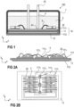
Figure 1 is a cross-sectional view of a power semiconductor module arrangement. -
Figure 2A is a cross-sectional view of another power semiconductor module arrangement. -
Figure 2B is a top view of the power semiconductor module arrangement ofFigure 2A . -
Figure 3A is a cross-sectional view of a power semiconductor module arrangement according to embodiments of the disclosure. -
Figure 3B is a top view of the power semiconductor module arrangement ofFigure 3A . -
Figure 4 is a cross-sectional view of a power semiconductor module arrangement according to further embodiments of the disclosure. -
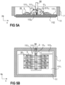
Figure 5A is a cross-sectional view of a power semiconductor module arrangement according to even further embodiments of the disclosure. -
Figure 5B is a top view of the power semiconductor module arrangement ofFigure 5A . -
Figure 6A is a cross-sectional view of a power semiconductor module arrangement according to even further embodiments of the disclosure. -
Figure 6B is a top view of the power semiconductor module arrangement ofFigure 6A . -
Figure 7 is a three-dimensional view of the power semiconductor module arrangement ofFigures 6A and 6B . - In the following detailed description, reference is made to the accompanying drawings. The drawings show specific examples in which the invention may be practiced. It is to be understood that the features and principles described with respect to the various examples may be combined with each other, unless specifically noted otherwise. In the description, as well as in the claims, designations of certain elements as "first element", "second element", "third element" etc. are not to be understood as enumerative. Instead, such designations serve solely to address different "elements". That is, e.g., the existence of a "third element" does not require the existence of a "first element" and a "second element". An electrical line or electrical connection as described herein may be a single electrically conductive element, or include at least two individual electrically conductive elements connected in series and/or parallel. Electrical lines and electrical connections may include metal and/or semiconductor material, and may be permanently electrically conductive (i.e., non-switchable). A semiconductor body as described herein may be made from (doped) semiconductor material and may be a semiconductor chip or be included in a semiconductor chip. A semiconductor body has electrically connecting pads and includes at least one semiconductor element with electrodes.
- Referring to
Figure 1 , a cross-sectional view of a powersemiconductor module arrangement 100 is schematically illustrated. The powersemiconductor module arrangement 100 includes ahousing 7 and asubstrate 10. Thesubstrate 10 includes adielectric insulation layer 11, a (structured)first metallization layer 111 attached to thedielectric insulation layer 11, and a (structured)second metallization layer 112 attached to thedielectric insulation layer 11. Thedielectric insulation layer 11 is disposed between the first andsecond metallization layers - Each of the first and
second metallization layers substrate 10 may be a ceramic substrate, that is, a substrate in which thedielectric insulation layer 11 is a ceramic, e.g., a thin ceramic layer. The ceramic may consist of or include one of the following materials: aluminum oxide; aluminum nitride; zirconium oxide; silicon nitride; boron nitride; or any other dielectric ceramic. For example, thedielectric insulation layer 11 may consist of or include one of the following materials: Al2O3, AlN, SiC, BeO or Si3N4. For instance, thesubstrate 10 may, e.g., be a Direct Copper Bonding (DCB) substrate, a Direct Aluminum Bonding (DAB) substrate, or an Active Metal Brazing (AMB) substrate. Further, thesubstrate 10 may be an Insulated Metal Substrate (IMS). An Insulated Metal Substrate generally comprises adielectric insulation layer 11 comprising (filled) materials such as epoxy resin or polyimide, for example. The material of thedielectric insulation layer 11 may be filled with ceramic particles, for example. Such particles may comprise, e.g., SiO2, Al2O3, AlN, or BN and may have a diameter of between about 1µm and about 50µm. Thesubstrate 10 may also be a conventional printed circuit board (PCB) having a non-ceramicdielectric insulation layer 11. For instance, a non-ceramicdielectric insulation layer 11 may consist of or include a cured resin. - The
substrate 10 is arranged in ahousing 7. In the example illustrated inFigure 1 , thesubstrate 10 is arranged on abase plate 12 which forms a ground surface of thehousing 7, while thehousing 7 itself solely comprises sidewalls and a cover. This, however, is only an example. It is also possible that thehousing 7 further comprises a ground surface and thesubstrate 10 and thebase plate 12 be arranged inside thehousing 7. In some powersemiconductor module arrangements 100, more than onesubstrate 10 is arranged on asingle base plate 12 or on the ground surface of ahousing 7. It is also possible that thesubstrate 10 itself forms a ground surface of thehousing 7. - One or
more semiconductor bodies 20 may be arranged on the at least onesubstrate 10. Each of thesemiconductor bodies 20 arranged on the at least onesubstrate 10 may include a diode, an IGBT (Insulated-Gate Bipolar Transistor), a MOSFET (Metal-Oxide-Semiconductor Field-Effect Transistor), a JFET (Junction Field-Effect Transistor), a HEMT (High-Electron-Mobility Transistor), and/or any other suitable semiconductor element. - The one or
more semiconductor bodies 20 may form a semiconductor arrangement on thesubstrate 10. InFigure 1 , only twosemiconductor bodies 20 are exemplarily illustrated. Thesecond metallization layer 112 of thesubstrate 10 inFigure 1 is a continuous layer. Thefirst metallization layer 111 is a structured layer in the example illustrated inFigure 1 . "Structured layer" means that thefirst metallization layer 111 is not a continuous layer, but includes recesses between different sections of the layer. Such recesses are schematically illustrated inFigure 1 . Thefirst metallization layer 111 in this example includes three different sections. This, however, is only an example. Any other number of sections is possible.Different semiconductor bodies 20 may be mounted to the same or to different sections of thefirst metallization layer 111. Different sections of thefirst metallization layer 111 may have no electrical connection or may be electrically connected to one or more other sections usingelectrical connection elements 3 such as, e.g., bonding wires or bonding ribbons.Electrical connections 3 may also include connection plates, conductor rails, or connection clips, for example, to name just a few examples. The one ormore semiconductor bodies 20 may be electrically and mechanically connected to thesubstrate 10 by a first electricallyconductive connection layer 30. The first electricallyconductive connection layer 30 may be a solder layer, a layer of an electrically conductive adhesive, or a layer of a sintered metal powder, e.g., a sintered silver powder, for example. According to other examples, it is also possible that thesecond metallization layer 112 is a structured layer. It is further possible to omit thesecond metallization layer 112 altogether. - The power
semiconductor module arrangement 100 illustrated inFigure 1 further includesterminal elements 4. Theterminal elements 4 are electrically connected to thefirst metallization layer 111 and provide an electrical connection between the inside and the outside of thehousing 7. Theterminal elements 4 may be electrically connected to thefirst metallization layer 111 with afirst end 41, while asecond end 42 of each of theterminal elements 4 protrudes out of thehousing 7. Theterminal elements 4 may be electrically contacted from the outside at their respective second ends 42. A first part of theterminal elements 4 may extend through the inside of thehousing 7 in a vertical direction y. The vertical direction y is a direction perpendicular to a top surface of thesubstrate 10, wherein the top surface of thesubstrate 10 is a surface on which the at least onesemiconductor body 20 is mounted. Theterminal elements 4 illustrated inFigure 1 , however, are only examples.Terminal elements 4 may be implemented in any other way and may be arranged anywhere within thehousing 7. For example, one or moreterminal elements 4 may be arranged close to or adjacent to the sidewalls of thehousing 7.Terminal elements 4 could also protrude through the sidewalls of thehousing 7 instead of through the cover. Thefirst end 41 of aterminal element 4 may be electrically and mechanically connected to thesubstrate 10 by an electrically conductive connection layer, for example (not explicitly illustrated inFigure 1 ). Such an electrically conductive connection layer may be a solder layer, a layer of an electrically conductive adhesive, or a layer of a sintered metal powder, e.g., a sintered silver (Ag) powder, for example. Thefirst end 41 of aterminal element 4 may also be electrically coupled to thesubstrate 10 via one or moreelectrical connections 3, for example. - The power
semiconductor module arrangement 100 may further include anencapsulant 5. Anencapsulant 5 may consist of or include a silicone gel or may be a rigid molding compound, for example. Theencapsulant 5 may at least partly fill the interior of thehousing 7, thereby covering the components and electrical connections that are arranged on thesubstrate 10. Theterminal elements 4 may be partly embedded in theencapsulant 5. At least their second ends 42, however, are not covered by theencapsulant 5 and protrude from theencapsulant 5 through thehousing 7 to the outside of thehousing 7. Theencapsulant 5 is configured to protect the components and electrical connections of thepower semiconductor module 100, in particular the components arranged on thesubstrate 10 inside thehousing 7, from certain environmental conditions and mechanical damage. - Now referring to
Figure 2A , a cross-sectional view of another power semiconductor module arrangement is schematically illustrated. The power semiconductor module arrangement ofFigure 2A essentially corresponds to the powersemiconductor module arrangement 100 as has been described with respect toFigure 1 above. Ahousing 7, anencapsulant 5, andterminal elements 4, however, are not specifically illustrated inFigure 2A. Figure 2B schematically illustrates a top view of the power semiconductor module arrangement ofFigure 2A . - In particular,
Figures 2A and 2B schematically illustrate asubstrate 10 comprising a structuredfirst metallization layer 111 arranged on a first side of thedielectric insulation layer 11 and comprising a plurality of different sections that are separate and distinct from each other. Thesemiconductor bodies 20 are mounted on afirst section 1111 of thefirst metallization layer 111. Each of the plurality ofsemiconductor bodies 20 comprises a control electrode and a controllable load path between a first load electrode and a second load electrode. The first load electrode of each of the plurality ofsemiconductor bodies 20 is electrically coupled to thefirst section 1111 of thefirst metallization layer 111, the second load electrode of each of the plurality ofsemiconductor bodies 20 is electrically coupled to asecond section 1112, of thefirst metallization layer 111, and the control electrode of each of the plurality ofsemiconductor bodies 20 is electrically coupled to one or morethird sections 1113 of thefirst metallization layer 111. In the example ofFigures 2A and 2B , threethird sections 1113 are schematically illustrated. The differentthird sections 1113 are separate and distinct from each other as well as from each of the other sections of thefirst metallization layer 111. The differentthird sections 1113, however, are all designated asthird sections 1113 herein, as they are all electrically coupled to the control electrode of one or more of the plurality ofsemiconductor bodies 20. Instead of a plurality (two or more) of separatethird sections 1113, a singlethird section 1113 could be provided instead. In the arrangement illustrated inFigures 2A and 2B , the one or morethird sections 1113 are horizontally surrounded by thesecond section 1112. That is, thethird sections 1113 form a plurality of islands that are surrounded by thesecond section 1112. Instead, the one or morethird sections 1113 could also be arranged beside thesecond section 1112 in any other way. All of the different sections of thefirst metallization layer 111, however, are arranged on thedielectric insulation layer 11 and in one and the same plane. This requires a significant amount of space on thedielectric insulation layer 11. The size of thedielectric insulation layer 11 in the power semiconductor module ofFigures 2A and 2B is chosen to be able to accommodate all of the different sections of thefirst metallization layer 111. Thesubstrate 10, therefore, has a comparably large size and the overall costs of the power semiconductor module are comparably high. - Now referring to
Figures 3A and 3B , a power semiconductor module arrangement according to embodiments of the disclosure is schematically illustrated, whereinFigure 3A schematically illustrates a cross-sectional view, andFigure 3B schematically illustrates a top view of the exemplary power semiconductor module arrangement. The power semiconductor module arrangement, instead of the one or morethird sections 1113 arranged on thedielectric insulation layer 11, comprises anadditional metallization layer 111A arranged in parallel to and distant from thefirst metallization layer 111. Theadditional metallization layer 111A is not arranged in the same plane as thefirst metallization layer 111. Instead, theadditional metallization layer 111A is arranged vertically above thefirst metallization layer 111. That is, a distance d1 between thefirst metallization layer 111 and theadditional metallization layer 111A in the vertical direction y is greater than zero. For example, the distance d1 may be at least 60µm, at least 100µm, or at least 150µm. The distance d1, however, may be less than 1000µm, or less than 500µm, for example. The distance d1 may be defined by the components that are arranged between thefirst metallization layer 111 and the additional metallization layer 111A (e.g., connection layer, dielectric insulation layer, connection clip, etc.), as will be described in further detail below. - The
semiconductor bodies 20 each may comprise a controllable semiconductor element, For example, thesemiconductor bodies 20 may be implemented as IGBTs (Insulated-Gate Bipolar Transistor), MOSFETs (Metal-Oxide-Semiconductor Field-Effect Transistor), JFETs (Junction Field-Effect Transistor), HEMTs (High-Electron-Mobility Transistor), and/or any other suitable controllable semiconductor elements. That is, eachsemiconductor body 20 comprises a first electrode, a second electrode and a third electrode, wherein the first electrode, the second electrode, and the third electrode are each a different one of the first load electrode, the second electrode, and the control electrode. The first load electrodes of the plurality ofsemiconductor bodies 20 may be drain electrodes, the second load electrodes of thesemiconductor bodies 20 may be source electrodes, and the control electrodes of thesemiconductor bodies 20 may be gate electrodes. According to another example, the first load electrodes of the plurality ofsemiconductor bodies 20 may be collector electrodes, the second load electrodes of thesemiconductor bodies 20 may be emitter electrodes, and the control electrodes of thesemiconductor bodies 20 may be base electrodes. According to one embodiment of the disclosure, the plurality ofsemiconductor bodies 20 are all of the same kind. That is, each of the plurality ofsemiconductor bodies 20 may be or may comprise an IGBTs, for example. It is, however, also possible that the plurality ofsemiconductor bodies 20 comprises two different kinds of controllable semiconductor elements. - The first load electrode of each of the plurality of
semiconductor bodies 20 may be electrically coupled to thefirst section 1111 of the first metallization layer (111) by means of a first electricallyconductive connection layer 30. The first electricallyconductive connection layer 30 may be a solder layer, a layer of an electrically conductive adhesive, or a layer of a sintered metal powder, e.g., a sintered silver (Ag) powder, for example. The second load electrode of each of the plurality ofsemiconductor bodies 20 may be electrically coupled to thesecond section 1112 of thefirst metallization layer 111 by means of one or moreelectrical connection elements 3 such as, e.g., bonding wires or bonding ribbons. The control electrode of each of the plurality ofsemiconductor bodies 20 may be electrically coupled to theadditional metallization layer 111A by means of one or moreelectrical connection elements 3. - As the
additional metallization layer 111A is arranged in an additional plane in parallel to thefirst metallization layer 111, less space is required on thedielectric insulation layer 11. Thesemiconductor bodies 20, during operation, generally generate a significant amount of heat. This heat is dissipated away from thesemiconductor bodies 20 through thedielectric insulation layer 11, e.g., towards a heat sink (not specifically illustrated). Theadditional metallization layer 111A is not directly coupled to thedielectric insulation layer 111. Any heat generated on theadditional metallization layer 111A, therefore, may not be conducted away as efficiently as heat generated on thefirst metallization layer 111. However, as theadditional metallization layer 111A is electrically coupled to the control electrodes of thesemiconductor bodies 20, only control signals are conducted through theadditional metallization layer 111A. Control signals usually comprise electrical signals of 15V or less and are configured to control the function of thedifferent semiconductor bodies 20. Control signals, however, may also comprise electrical signals of more than 15V. In any case, however, control signals comprise electrical signals of voltages and currents that are significantly lower than the common supply voltages / load currents. The power semiconductor module arrangement may switch from an off state (non-working state) to an on state (working state), for example, when a supply voltage is provided. Supply voltages may be voltages of more than 100V, for example. Due to the comparably low voltages and low currents of the control signals only an insignificant amount of heat is generated in theadditional metallization layer 111A. Arranging theadditional metallization layer 111A distant from thedielectric insulation layer 11, therefore, is not critical in view of overheating. - In the embodiments of the disclosure described with respect to
Figures 3A and 3B , theadditional metallization layer 111A is arranged on an additionaldielectric insulation layer 11A, wherein the additionaldielectric insulation layer 11A is arranged in parallel to and distant from thedielectric insulation layer 11, and wherein the additionaldielectric insulation layer 11A is arranged between theadditional metallization layer 111A and thefirst metallization layer 111. In this way, theadditional metallization layer 111A is electrically insulated from thefirst metallization layer 111. The additionaldielectric insulation layer 11A may be coupled to thefirst metallization layer 111 by means of asecond connection layer 32. Thesecond connection layer 32 may be a solder layer, a layer of an electrically conductive adhesive, a layer of an electrically insulating adhesive, or a layer of a sintered metal powder. In the example illustrated inFigure 3A , an additionalsecond metallization layer 112A is arranged between the additionaldielectric insulation layer 11A and thesecond connection layer 32. Therefore, solder or sintering techniques may be used, for example, in order to couple the additionaldielectric insulation layer 11A with the additionalsecond metallization layer 112A arranged thereon to thefirst metallization layer 111. It is, however, also possible to glue the additionaldielectric insulation layer 11A with the additionalsecond metallization layer 112A arranged thereon to thefirst metallization layer 111, using an electrically conductive or an electrically insulating adhesive, for example. - It is also possible that the additional
second metallization layer 112A be omitted, as is schematically illustrated inFigure 4 . That is, the additionaldielectric insulation layer 11A may be directly attached to thefirst metallization layer 111. In this case, soldering or sintering the additionaldielectric insulation layer 11A to thefirst metallization layer 111 may not be possible. The additionaldielectric insulation layer 11A may be glued to thefirst metallization layer 111 using an electrically conducting or an electrically insulating adhesive, for example. The additionalsecond metallization layer 112A generally has no function that is required for the operation of the power semiconductor module. That is, the sole function of the additionalsecond metallization layer 112A may be to facilitate mounting the additionaldielectric insulation layer 11A with theadditional metallization layer 111A arranged thereon to thefirst metallization layer 111. - The additional
dielectric insulation layer 11A may be arranged on and mechanically coupled to thesecond section 1112 of thefirst metallization layer 111. It is, however, also possible to arrange the additionaldielectric insulation layer 11A on any other section of thefirst metallization layer 111. As is schematically illustrated inFigure 3B , for example, theadditional metallization layer 111A may be electrically coupled to afourth section 1114 of thefirst metallization layer 111 by means of one or moreelectrical connection elements 3. Thefourth section 1114 of thefirst metallization layer 111 may be electrically contacted by means of one or moreterminal elements 4, as has been described with respect toFigure 1 above, for example (terminal elements not specifically illustrated inFigure 3B ). - Alternatively, it is also possible that the
additional metallization layer 111A be electrically coupled to aterminal element 90 extending vertically through a sidewall of thehousing 7, as is schematically illustrated inFigures 5A and 5B . Theadditional metallization layer 111A may be electrically coupled to theterminal element 90 by means of one or moreelectrical connection elements 3, for example. Theterminal element 90 may be molded into the sidewall of thehousing 7, for example, or may be arranged in a vertical hole extending through the sidewall of thehousing 7. Theadditional metallization layer 111A, however, may also be electrically contacted from outside of thehousing 7 in any other suitable way. For example, theadditional metallization layer 111A may be electrically contacted by mans ofterminal elements 4, similar to what has been described with respect toFigure 1 above. - Arranging the
additional metallization layer 111A on an additionaldielectric insulation layer 11A and mounting the additionaldielectric insulation layer 11A to a section of thefirst metallization layer 111, however, is only an example. Now referring toFigures 6A and 6B , the power semiconductor module arrangement may comprise aconnection clip 34. Theconnection clip 34 may comprise a layer of an electrically conducting material having a thickness t34 in a vertical direction y that is significantly smaller than its length l34 in a first horizontal direction x and its width w34 in a second horizontal direction z. For example, the thickness t34 of theconnection clip 34 may be between 50µm and 300µm. The length l34 and width w34 of theconnection clip 34 may be in the range of several millimeters up to several tens of millimeters, for example. Theconnection clip 34 may comprise or consist of copper, for example. Any other electrically conducting materials, however, are also possible. Theconnection clip 34 can essentially be regarded as an extensive metallic layer that is used to electrically couple the second load electrode of each of the plurality ofsemiconductor bodies 20 to thesecond section 1112 of thefirst metallization layer 111. Theconnection clip 34 may have any suitable regular or irregular shape. Instead ofelectrical connection elements 3 such as, e.g., bonding wires or bonding ribbons (see, e.g.,Figures 3, 4 and5 ), theconnection clip 34 may be used to electrically couple the second load electrode of each of the plurality ofsemiconductor bodies 20 to thesecond section 1112 of thefirst metallization layer 111. Theconnection clip 34 may replace any other kind ofelectrical connection elements 3. Oneelectrical connection element 3 usually electrically couples asingle semiconductor body 20 to the respective section of thefirst metallization layer 111. Theextensive connection clip 34 electrically couples a plurality ofsemiconductor bodies 20 to one and the same section of thefirst metallization layer 111. - As the
connection clip 34 is an extensive element, it provides a surface area (surface facing away from the substrate 10) that is large enough to easily accommodate the additionaldielectric insulation layer 11A with theadditional metallization layer 111A arranged thereon. As is schematically illustrated in the cross-sectional view ofFigure 6A , theadditional metallization layer 111A is arranged on theconnection clip 34, with the additionaldielectric insulation layer 11A arranged between theconnection clip 34 and theadditional metallization layer 111A. Similar to what has been described above, an additionalsecond metallization layer 112A may be arranged between the additionaldielectric insulation layer 11A and theconnection clip 34. The additionalsecond metallization layer 112A, however, can also be omitted. The additionaldielectric insulation layer 11A with theadditional metallization layer 111A arranged thereon may be mounted to theconnection clip 34 similar to what has been described above with respect toFigures 3, 4 and5 . That is, the additionaldielectric insulation layer 11A may be attached to the connection clip 34 (instead of to the first metallization layer 111) by means of asecond connection layer 32. If the additionalsecond metallization layer 112A is present, thesecond connection layer 32 may be a solder layer, a layer of an electrically conductive adhesive, a layer of an electrically insulating adhesive, or a layer of a sintered metal powder, for example. If the additionalsecond metallization layer 112A is omitted, the additionaldielectric insulation layer 11A may be glued to theconnection clip 34, using an electrically conductive or an electrically insulating adhesive, for example. - The additional
dielectric insulation layer 11A with theadditional metallization layer 111A and the optional additionalsecond metallization layer 112A arranged thereon may be implemented as a so-called flex-board (flexible printed circuit board). Conventional stiff or rigid printed circuit boards could also be used, for example. That is, the additionaldielectric insulation layer 11A may consist of a polymer, for example. Thedielectric insulation layer 11 on the other hand, may consist of a ceramic material, similar to what has been described with respect toFigure 1 above. Thesubstrate 10, however, may also be a conventional printed circuit board (PCB) having a non-ceramicdielectric insulation layer 11. For instance, a non-ceramicdielectric insulation layer 11 may consist of or include a cured resin. It is, however, generally also possible that the additionaldielectric insulation layer 11A is a ceramic layer, similar to thedielectric insulation layer 11. That is, the additionaldielectric insulation layer 11A with theadditional metallization layer 111A and the optional additionalsecond metallization layer 112A arranged thereon may also be implemented as a conventional ceramic substrate (e.g., IMS, FPC, DCB, AMB, Al2O3, AlN, or Si3N4 substrate). The additionaldielectric insulation layer 11A generally provides sufficient dielectric insulation between theadditional metallization layer 111A and thefirst metallization layer 111, or between theadditional metallization layer 111A and theconnection clip 34. As has been described above, theadditional metallization layer 111A carries comparably small voltages and currents. The requirements concerning dielectric insulation, therefore, are comparably low. - As is illustrated in
Figures 3, 4 and5 , only theadditional metallization layer 111A may be provided on the surface of the additionaldielectric insulation layer 11A facing away from thesubstrate 10.Figure 7 schematically illustrates a three-dimensional view of an embodiment similar to the embodiment ofFigure 6 comprising only theadditional metallization layer 111A on the surface of the additionaldielectric insulation layer 11A facing away from thesubstrate 10. It is, however, also possible that further metallization layers are provided on the additionaldielectric insulation layer 11A. This is exemplarily illustrated inFigures 6A and 6B . In this example, onefurther metallization layer 111E is arranged on the surface of the additionaldielectric insulation layer 11A facing away from thesubstrate 10. Thisfurther metallization layer 111E may be electrically coupled to an auxiliary emitter of each of the plurality ofsemiconductor bodies 20 by means of one or moreelectrical connection elements 3, for example. Thefurther metallization layer 111E is only specifically illustrated with regard to the embodiments comprising aconnection 34, but may be implemented in similar ways in other embodiments not comprising aconnection clip 34. The at least onefurther metallization layer 111E may be electrically coupled to arespective section 1115 of thefirst metallization layer 111 by means of one or moreelectrical connection elements 3, for example, similar to what has been described with respect to the additional metallization layer 111A (see, e.g.,Figure 6B ). The at least onefurther metallization layer 111E, however, can also be electrically contacted in any other suitable way. - Now referring to all
Figures 3 to 6 , theadditional metallization layer 111A, and anyfurther metallization layers 111E arranged on the additionaldielectric insulation layer 11A, may have a thickness t111A in the vertical direction y of up to 35µm, up to 50µm, up to 75µm, or up to 500µm. For example, the thickness t111A of theadditional metallization layer 111A may be between 20µm and 500µm for ceramic substrates or conventional printed circuit boards, or between 35µm to 75µm, possibly even between 35µm and 105µm for flex-boards. Theadditional metallization layer 111A may comprise or consist of copper or aluminum, for example. The same applies for the optional additionalsecond metallization layer 112A. The additionaldielectric insulation layer 11A may have a thickness t11A in the vertical direction y of at least 50µm, at least 100µm, or at least 150µm. - A cross-sectional area of the
dielectric insulation layer 111 may be significantly larger than a cross-sectional area of the additionaldielectric insulation layer 11A. For example, the cross-sectional area of thedielectric insulation layer 111 may be at least ten times or at least 20 times larger than a cross-sectional area of the additionaldielectric insulation layer 11A. - The additional
dielectric insulation layer 11A with theadditional metallization layer 111A, the (optional) additionalsecond metallization layer 112A, and anyfurther metallization layers 111E arranged thereon may be mounted to aconnection clip 34 before theconnection clip 34 is stamped (cut) from a large metal sheet, or after theconnection clip 34 has been stamped (cut) from a large metal sheet but before it has been bent in any way, or after stamping (cutting) and bending theconnection clip 34 but before mounting it to thesubstrate 10, or even after mounting theconnection clip 34 to thesubstrate 10. - In the examples described above, the control electrode of each of the plurality of
semiconductor bodies 20 is electrically coupled to anadditional metallization layer 111A, while the first load electrode and the second load electrode of each of thesemiconductor bodies 20 is electrically coupled to a respective section of thefirst metallization layer 111 arranged on thedielectric insulation layer 11. However, it is generally also possible that instead of the control electrodes, the first load electrodes or the second load electrodes of thesemiconductor bodies 20 are electrically coupled to theadditional metallization layer 111A. For example, the first load electrodes of the plurality ofsemiconductor bodies 20 may be electrically coupled to afirst section 1111 of thefirst metallization layer 111, the control electrodes of the plurality ofsemiconductor bodies 20 may be electrically coupled to asecond section 1112 of thefirst metallization layer 111, and the second load electrodes of the plurality ofsemiconductor bodies 20 may be electrically coupled to theadditional metallization layer 111A. Generally speaking, a first electrode (e.g., gate, emitter, collector, source, drain) may be electrically coupled to theadditional metallization layer 111A, while a second and a third electrode of the plurality ofsemiconductor bodies 20, which are different from the first electrode, are electrically coupled to respective sections of thefirst metallization layer 111.
Claims (15)
- A power semiconductor module arrangement comprises,a substrate (10) comprising a dielectric insulation layer (11) and a first metallization layer (111) arranged on a first side of the dielectric insulation layer (11), wherein the first metallization layer (111) comprises a plurality of different sections that are separate and distinct from each other; anda plurality of semiconductor bodies (20) arranged on the first metallization layer (111), whereina first electrode of each of the plurality of semiconductor bodies (20) is electrically coupled to a first section (1111) of the first metallization layer (111),a second electrode of each of the plurality of semiconductor bodies (20) is electrically coupled to a second section (1112) of the first metallization layer (111),a third electrode of each of the plurality of semiconductor bodies (20) is electrically coupled to an additional metallization layer (111A) by means of one or more electrical connection elements (3),the additional metallization layer (111A) is arranged distant from and in parallel to the first metallization layer (111), andthe additional metallization layer (111A) is arranged on an additional dielectric insulation layer (11A), wherein the additional dielectric insulation layer (11A) is arranged in parallel to and distant from the dielectric insulation layer (11), and wherein the additional dielectric insulation layer (11A) is arranged between the additional metallization layer (111A) and the first metallization layer (111).
- The power semiconductor module arrangement of claim 1, whereinthe first electrode of each of the plurality of semiconductor bodies (20) is electrically coupled to the first section (1111) of the first metallization layer (111) by means of a first electrically conductive connection layer (30);the second electrode of each of the plurality of semiconductor bodies (20) is electrically coupled to the second section (1112) of the first metallization layer (111) by means of one or more electrical connection elements (3); andthe third electrode of each of the plurality of semiconductor bodies (20) is electrically coupled to the additional metallization layer (111A) by means of one or more electrical connection elements (3).
- The power semiconductor module arrangement of claim 2, wherein an electrical connection element (3) comprises a bonding wire, a bonding ribbon, a connection plate, a conductor rail, or a connection clip.
- The power semiconductor module arrangement of any of the preceding claims, whereineach of the plurality of semiconductor bodies (20) comprises a control electrode and a controllable load path between a first load electrode and a second load electrode, andthe first electrode, the second electrode, and the third electrode are each a different one of the first load electrode, the second load electrode, and the control electrode.
- The power semiconductor module arrangement of any of the preceding claims, wherein the additional dielectric insulation layer (11A) is coupled to the first metallization layer (111) by means of a second connection layer (32).
- The power semiconductor module arrangement of claim 5, wherein the second connection layer (32) is a solder layer, a layer of an electrically conductive adhesive, a layer of an electrically insulating adhesive, or a layer of a sintered metal powder.
- The power semiconductor module arrangement of claim 5 or 6, further comprising an additional second metallization layer (112A) arranged between the additional dielectric insulation layer (11A) and the second connection layer (32).
- The power semiconductor module arrangement of any of the preceding claims, wherein the additional dielectric insulation layer (11A) is coupled to the second section (1112) of the first metallization layer (111).
- The power semiconductor module arrangement of any of claims 1 to 4, further comprising a connection clip (34), the connection clip (34) comprising a layer of an electrically conducting material having a thickness (t34) in a vertical direction (y) that is significantly smaller than its length (l34) in a first horizontal direction (x) and its width (w34) in a second horizontal direction (z), wherein the second electrode of each of the plurality of semiconductor bodies (20) is electrically coupled to the second section (1112) of the first metallization layer (111) by means of the connection clip (34).
- The power semiconductor module arrangement of claim 9, wherein the additional dielectric insulation layer (11A) is coupled to the connection clip (34) by means of a second connection layer (32), wherein the connection clip (34) is arranged between the additional dielectric insulation layer (11A) and the second section (1112) of the first metallization layer (111).
- The power semiconductor module arrangement of any of the preceding claims, wherein the additional metallization layer (111A) is electrically coupled to a fourth section (1114) of the first metallization layer (111) by means of one or more electrical connection elements (3).
- The power semiconductor module arrangement of any of claims 1 to 10, further comprising a housing (7) and a terminal element (90) extending vertically through a sidewall of the housing (7), wherein the additional metallization layer (111A) is electrically coupled to the terminal element (90) by means of one or more electrical connection elements (3).
- The power semiconductor module arrangement of any of the preceding claims, wherein the dielectric insulation layer (11) consists of a ceramic material, and the additional dielectric insulation layer (11A) consists of a polymer or a ceramic material.
- The power semiconductor module arrangement of any of the preceding claims, wherein the additional metallization layer (111A) has a thickness (t111A) in the vertical direction (y) of up to 35µm, up to 50µm, up to 75µm, or up to 500µm.
- The power semiconductor module arrangement of any of the preceding claims, wherein the additional dielectric insulation layer (11A) has a thickness (t11A) in the vertical direction (y) of at least 50µm, at least 100µm, or at least 150µm.
Priority Applications (1)
| Application Number | Priority Date | Filing Date | Title |
|---|---|---|---|
| EP23158107.5A EP4421868B1 (en) | 2023-02-23 | 2023-02-23 | Semiconductor module arrangement |
Applications Claiming Priority (1)
| Application Number | Priority Date | Filing Date | Title |
|---|---|---|---|
| EP23158107.5A EP4421868B1 (en) | 2023-02-23 | 2023-02-23 | Semiconductor module arrangement |
Publications (2)
| Publication Number | Publication Date |
|---|---|
| EP4421868A1 true EP4421868A1 (en) | 2024-08-28 |
| EP4421868B1 EP4421868B1 (en) | 2024-12-25 |
Family
ID=85382755
Family Applications (1)
| Application Number | Title | Priority Date | Filing Date |
|---|---|---|---|
| EP23158107.5A Active EP4421868B1 (en) | 2023-02-23 | 2023-02-23 | Semiconductor module arrangement |
Country Status (1)
| Country | Link |
|---|---|
| EP (1) | EP4421868B1 (en) |
Citations (3)
| Publication number | Priority date | Publication date | Assignee | Title |
|---|---|---|---|---|
| US20160056132A1 (en) * | 2014-08-20 | 2016-02-25 | Infineon Technologies Ag | Low-Inductance Circuit Arrangement Comprising Load Current Collecting Conductor Track |
| US20200286865A1 (en) * | 2019-03-06 | 2020-09-10 | Semiconductor Components Industries, Llc | Semiconductor Package and Related Methods |
| EP4064340A1 (en) * | 2021-03-24 | 2022-09-28 | Hitachi Energy Switzerland AG | Power semiconductor module and manufacturing method |
-
2023
- 2023-02-23 EP EP23158107.5A patent/EP4421868B1/en active Active
Patent Citations (3)
| Publication number | Priority date | Publication date | Assignee | Title |
|---|---|---|---|---|
| US20160056132A1 (en) * | 2014-08-20 | 2016-02-25 | Infineon Technologies Ag | Low-Inductance Circuit Arrangement Comprising Load Current Collecting Conductor Track |
| US20200286865A1 (en) * | 2019-03-06 | 2020-09-10 | Semiconductor Components Industries, Llc | Semiconductor Package and Related Methods |
| EP4064340A1 (en) * | 2021-03-24 | 2022-09-28 | Hitachi Energy Switzerland AG | Power semiconductor module and manufacturing method |
Also Published As
| Publication number | Publication date |
|---|---|
| EP4421868B1 (en) | 2024-12-25 |
Similar Documents
| Publication | Publication Date | Title |
|---|---|---|
| JP2023042566A (en) | Semiconductor device | |
| US11942449B2 (en) | Semiconductor arrangement and method for producing the same | |
| EP2889902B1 (en) | Electric power semiconductor device | |
| EP3690937B1 (en) | Cascode semiconductor device and method of manufacture | |
| EP4040472A1 (en) | A semiconductor device and a method of manufacturing a semiconductor device | |
| US20240203808A1 (en) | Semiconductor device | |
| EP4084062A1 (en) | Power semiconductor module arrangement | |
| US11282774B2 (en) | Power semiconductor module arrangement | |
| EP4421868B1 (en) | Semiconductor module arrangement | |
| US20210028078A1 (en) | Semiconductor Module Arrangement | |
| US20230170286A1 (en) | Terminal Element or Bus Bar, and Power Semiconductor Module Arrangement Comprising a Terminal Element or Bus Bar | |
| EP4307359A1 (en) | Power semiconductor module arrangement and method for producing the same | |
| US20240203950A1 (en) | Semiconductor module arrangement | |
| EP4113605B1 (en) | Power semiconductor module arrangement | |
| US12002794B2 (en) | Semiconductor device | |
| EP4345884A1 (en) | Power semiconductor module arrangement and printed circuit board for a power semiconductor module arrangement | |
| EP4607584A1 (en) | Semiconductor module arrangement | |
| US20240304538A1 (en) | Semiconductor module arrangement | |
| EP4270466A1 (en) | Power semiconductor module arrangements and methods for producing power semiconductor module arrangements | |
| US12002740B2 (en) | Printed circuit board, power semiconductor module arrangement comprising a printed circuit board, and method for assembling the same | |
| EP4700827A1 (en) | Power semiconductor module arrangement | |
| EP4372807B1 (en) | Substrate arrangement and methods for producing a substrate arrangement | |
| EP4422358A1 (en) | Substrate | |
| US20260090317A1 (en) | System and method for mounting a housing to a base plate of a semiconductor module | |
| US20260090385A1 (en) | Semiconductor module comprising a housing |
Legal Events
| Date | Code | Title | Description |
|---|---|---|---|
| PUAI | Public reference made under article 153(3) epc to a published international application that has entered the european phase |
Free format text: ORIGINAL CODE: 0009012 |
|
| STAA | Information on the status of an ep patent application or granted ep patent |
Free format text: STATUS: REQUEST FOR EXAMINATION WAS MADE |
|
| 17P | Request for examination filed |
Effective date: 20230914 |
|
| AK | Designated contracting states |
Kind code of ref document: A1 Designated state(s): AL AT BE BG CH CY CZ DE DK EE ES FI FR GB GR HR HU IE IS IT LI LT LU LV MC ME MK MT NL NO PL PT RO RS SE SI SK SM TR |
|
| GRAP | Despatch of communication of intention to grant a patent |
Free format text: ORIGINAL CODE: EPIDOSNIGR1 |
|
| STAA | Information on the status of an ep patent application or granted ep patent |
Free format text: STATUS: GRANT OF PATENT IS INTENDED |
|
| RIC1 | Information provided on ipc code assigned before grant |
Ipc: H01L 23/498 20060101ALN20240829BHEP Ipc: H01L 23/48 20060101ALN20240829BHEP Ipc: H01L 23/24 20060101ALI20240829BHEP Ipc: H01L 23/053 20060101ALI20240829BHEP Ipc: H01L 23/373 20060101ALI20240829BHEP Ipc: H01L 23/538 20060101ALI20240829BHEP Ipc: H01L 25/07 20060101AFI20240829BHEP |
|
| INTG | Intention to grant announced |
Effective date: 20240911 |
|
| GRAS | Grant fee paid |
Free format text: ORIGINAL CODE: EPIDOSNIGR3 |
|
| GRAA | (expected) grant |
Free format text: ORIGINAL CODE: 0009210 |
|
| STAA | Information on the status of an ep patent application or granted ep patent |
Free format text: STATUS: THE PATENT HAS BEEN GRANTED |
|
| P01 | Opt-out of the competence of the unified patent court (upc) registered |
Free format text: CASE NUMBER: APP_60520/2024 Effective date: 20241111 |
|
| AK | Designated contracting states |
Kind code of ref document: B1 Designated state(s): AL AT BE BG CH CY CZ DE DK EE ES FI FR GB GR HR HU IE IS IT LI LT LU LV MC ME MK MT NL NO PL PT RO RS SE SI SK SM TR |
|
| REG | Reference to a national code |
Ref country code: GB Ref legal event code: FG4D |
|
| REG | Reference to a national code |
Ref country code: CH Ref legal event code: EP |
|
| REG | Reference to a national code |
Ref country code: DE Ref legal event code: R096 Ref document number: 602023001440 Country of ref document: DE |
|
| REG | Reference to a national code |
Ref country code: IE Ref legal event code: FG4D |
|
| REG | Reference to a national code |
Ref country code: LT Ref legal event code: MG9D |
|
| PG25 | Lapsed in a contracting state [announced via postgrant information from national office to epo] |
Ref country code: HR Free format text: LAPSE BECAUSE OF FAILURE TO SUBMIT A TRANSLATION OF THE DESCRIPTION OR TO PAY THE FEE WITHIN THE PRESCRIBED TIME-LIMIT Effective date: 20241225 |
|
| PG25 | Lapsed in a contracting state [announced via postgrant information from national office to epo] |
Ref country code: FI Free format text: LAPSE BECAUSE OF FAILURE TO SUBMIT A TRANSLATION OF THE DESCRIPTION OR TO PAY THE FEE WITHIN THE PRESCRIBED TIME-LIMIT Effective date: 20241225 |
|
| PG25 | Lapsed in a contracting state [announced via postgrant information from national office to epo] |
Ref country code: BG Free format text: LAPSE BECAUSE OF FAILURE TO SUBMIT A TRANSLATION OF THE DESCRIPTION OR TO PAY THE FEE WITHIN THE PRESCRIBED TIME-LIMIT Effective date: 20241225 |
|
| PG25 | Lapsed in a contracting state [announced via postgrant information from national office to epo] |
Ref country code: NO Free format text: LAPSE BECAUSE OF FAILURE TO SUBMIT A TRANSLATION OF THE DESCRIPTION OR TO PAY THE FEE WITHIN THE PRESCRIBED TIME-LIMIT Effective date: 20250325 |
|
| PG25 | Lapsed in a contracting state [announced via postgrant information from national office to epo] |
Ref country code: GR Free format text: LAPSE BECAUSE OF FAILURE TO SUBMIT A TRANSLATION OF THE DESCRIPTION OR TO PAY THE FEE WITHIN THE PRESCRIBED TIME-LIMIT Effective date: 20250326 Ref country code: LV Free format text: LAPSE BECAUSE OF FAILURE TO SUBMIT A TRANSLATION OF THE DESCRIPTION OR TO PAY THE FEE WITHIN THE PRESCRIBED TIME-LIMIT Effective date: 20241225 |
|
| PGFP | Annual fee paid to national office [announced via postgrant information from national office to epo] |
Ref country code: AT Payment date: 20250417 Year of fee payment: 3 |
|
| PG25 | Lapsed in a contracting state [announced via postgrant information from national office to epo] |
Ref country code: RS Free format text: LAPSE BECAUSE OF FAILURE TO SUBMIT A TRANSLATION OF THE DESCRIPTION OR TO PAY THE FEE WITHIN THE PRESCRIBED TIME-LIMIT Effective date: 20250325 |
|
| REG | Reference to a national code |
Ref country code: NL Ref legal event code: MP Effective date: 20241225 |
|
| PG25 | Lapsed in a contracting state [announced via postgrant information from national office to epo] |
Ref country code: NL Free format text: LAPSE BECAUSE OF FAILURE TO SUBMIT A TRANSLATION OF THE DESCRIPTION OR TO PAY THE FEE WITHIN THE PRESCRIBED TIME-LIMIT Effective date: 20241225 |
|
| REG | Reference to a national code |
Ref country code: AT Ref legal event code: MK05 Ref document number: 1754948 Country of ref document: AT Kind code of ref document: T Effective date: 20241225 |
|
| PG25 | Lapsed in a contracting state [announced via postgrant information from national office to epo] |
Ref country code: SM Free format text: LAPSE BECAUSE OF FAILURE TO SUBMIT A TRANSLATION OF THE DESCRIPTION OR TO PAY THE FEE WITHIN THE PRESCRIBED TIME-LIMIT Effective date: 20241225 |
|
| PG25 | Lapsed in a contracting state [announced via postgrant information from national office to epo] |
Ref country code: PL Free format text: LAPSE BECAUSE OF FAILURE TO SUBMIT A TRANSLATION OF THE DESCRIPTION OR TO PAY THE FEE WITHIN THE PRESCRIBED TIME-LIMIT Effective date: 20241225 |
|
| PGFP | Annual fee paid to national office [announced via postgrant information from national office to epo] |
Ref country code: DE Payment date: 20250422 Year of fee payment: 3 |
|
| PG25 | Lapsed in a contracting state [announced via postgrant information from national office to epo] |
Ref country code: ES Free format text: LAPSE BECAUSE OF FAILURE TO SUBMIT A TRANSLATION OF THE DESCRIPTION OR TO PAY THE FEE WITHIN THE PRESCRIBED TIME-LIMIT Effective date: 20241225 |
|
| PG25 | Lapsed in a contracting state [announced via postgrant information from national office to epo] |
Ref country code: IS Free format text: LAPSE BECAUSE OF FAILURE TO SUBMIT A TRANSLATION OF THE DESCRIPTION OR TO PAY THE FEE WITHIN THE PRESCRIBED TIME-LIMIT Effective date: 20250425 |
|
| PG25 | Lapsed in a contracting state [announced via postgrant information from national office to epo] |
Ref country code: PT Free format text: LAPSE BECAUSE OF FAILURE TO SUBMIT A TRANSLATION OF THE DESCRIPTION OR TO PAY THE FEE WITHIN THE PRESCRIBED TIME-LIMIT Effective date: 20250428 |
|
| PG25 | Lapsed in a contracting state [announced via postgrant information from national office to epo] |
Ref country code: EE Free format text: LAPSE BECAUSE OF FAILURE TO SUBMIT A TRANSLATION OF THE DESCRIPTION OR TO PAY THE FEE WITHIN THE PRESCRIBED TIME-LIMIT Effective date: 20241225 |
|
| PG25 | Lapsed in a contracting state [announced via postgrant information from national office to epo] |
Ref country code: RO Free format text: LAPSE BECAUSE OF FAILURE TO SUBMIT A TRANSLATION OF THE DESCRIPTION OR TO PAY THE FEE WITHIN THE PRESCRIBED TIME-LIMIT Effective date: 20241225 Ref country code: AT Free format text: LAPSE BECAUSE OF FAILURE TO SUBMIT A TRANSLATION OF THE DESCRIPTION OR TO PAY THE FEE WITHIN THE PRESCRIBED TIME-LIMIT Effective date: 20241225 |
|
| PG25 | Lapsed in a contracting state [announced via postgrant information from national office to epo] |
Ref country code: SK Free format text: LAPSE BECAUSE OF FAILURE TO SUBMIT A TRANSLATION OF THE DESCRIPTION OR TO PAY THE FEE WITHIN THE PRESCRIBED TIME-LIMIT Effective date: 20241225 |
|
| PG25 | Lapsed in a contracting state [announced via postgrant information from national office to epo] |
Ref country code: CZ Free format text: LAPSE BECAUSE OF FAILURE TO SUBMIT A TRANSLATION OF THE DESCRIPTION OR TO PAY THE FEE WITHIN THE PRESCRIBED TIME-LIMIT Effective date: 20241225 |
|
| PG25 | Lapsed in a contracting state [announced via postgrant information from national office to epo] |
Ref country code: IT Free format text: LAPSE BECAUSE OF FAILURE TO SUBMIT A TRANSLATION OF THE DESCRIPTION OR TO PAY THE FEE WITHIN THE PRESCRIBED TIME-LIMIT Effective date: 20241225 |
|
| PG25 | Lapsed in a contracting state [announced via postgrant information from national office to epo] |
Ref country code: SE Free format text: LAPSE BECAUSE OF FAILURE TO SUBMIT A TRANSLATION OF THE DESCRIPTION OR TO PAY THE FEE WITHIN THE PRESCRIBED TIME-LIMIT Effective date: 20241225 |
|
| PG25 | Lapsed in a contracting state [announced via postgrant information from national office to epo] |
Ref country code: MC Free format text: LAPSE BECAUSE OF FAILURE TO SUBMIT A TRANSLATION OF THE DESCRIPTION OR TO PAY THE FEE WITHIN THE PRESCRIBED TIME-LIMIT Effective date: 20241225 |
|
| REG | Reference to a national code |
Ref country code: DE Ref legal event code: R097 Ref document number: 602023001440 Country of ref document: DE |
|
| PG25 | Lapsed in a contracting state [announced via postgrant information from national office to epo] |
Ref country code: DK Free format text: LAPSE BECAUSE OF FAILURE TO SUBMIT A TRANSLATION OF THE DESCRIPTION OR TO PAY THE FEE WITHIN THE PRESCRIBED TIME-LIMIT Effective date: 20241225 |
|
| PG25 | Lapsed in a contracting state [announced via postgrant information from national office to epo] |
Ref country code: LU Free format text: LAPSE BECAUSE OF NON-PAYMENT OF DUE FEES Effective date: 20250223 |
|
| PLBE | No opposition filed within time limit |
Free format text: ORIGINAL CODE: 0009261 |
|
| STAA | Information on the status of an ep patent application or granted ep patent |
Free format text: STATUS: NO OPPOSITION FILED WITHIN TIME LIMIT |
|
| REG | Reference to a national code |
Ref country code: DE Ref legal event code: R079 Ref document number: 602023001440 Country of ref document: DE Free format text: PREVIOUS MAIN CLASS: H01L0025070000 Ipc: H10D0080200000 |
|
| 26N | No opposition filed |
Effective date: 20250926 |
|
| REG | Reference to a national code |
Ref country code: BE Ref legal event code: MM Effective date: 20250228 |
|
| PG25 | Lapsed in a contracting state [announced via postgrant information from national office to epo] |
Ref country code: FR Free format text: LAPSE BECAUSE OF NON-PAYMENT OF DUE FEES Effective date: 20250225 |
|
| PG25 | Lapsed in a contracting state [announced via postgrant information from national office to epo] |
Ref country code: BE Free format text: LAPSE BECAUSE OF NON-PAYMENT OF DUE FEES Effective date: 20250228 |
|
| PG25 | Lapsed in a contracting state [announced via postgrant information from national office to epo] |
Ref country code: IE Free format text: LAPSE BECAUSE OF NON-PAYMENT OF DUE FEES Effective date: 20250223 |