EP4421551A1 - Mems device, in particular of mirror type, with improved detection of the deformation of a deformable structure of the same, and manufacturing process of the mems device - Google Patents
Mems device, in particular of mirror type, with improved detection of the deformation of a deformable structure of the same, and manufacturing process of the mems device Download PDFInfo
- Publication number
- EP4421551A1 EP4421551A1 EP24156497.0A EP24156497A EP4421551A1 EP 4421551 A1 EP4421551 A1 EP 4421551A1 EP 24156497 A EP24156497 A EP 24156497A EP 4421551 A1 EP4421551 A1 EP 4421551A1
- Authority
- EP
- European Patent Office
- Prior art keywords
- detection
- piezoelectric
- region
- actuation
- electrical connection
- Prior art date
- Legal status (The legal status is an assumption and is not a legal conclusion. Google has not performed a legal analysis and makes no representation as to the accuracy of the status listed.)
- Granted
Links
Images










Classifications
-
- G—PHYSICS
- G02—OPTICS
- G02B—OPTICAL ELEMENTS, SYSTEMS OR APPARATUS
- G02B26/00—Optical devices or arrangements for the control of light using movable or deformable optical elements
- G02B26/08—Optical devices or arrangements for the control of light using movable or deformable optical elements for controlling the direction of light
- G02B26/0816—Optical devices or arrangements for the control of light using movable or deformable optical elements for controlling the direction of light by means of one or more reflecting elements
- G02B26/0833—Optical devices or arrangements for the control of light using movable or deformable optical elements for controlling the direction of light by means of one or more reflecting elements the reflecting element being a micromechanical device, e.g. a MEMS mirror, DMD
- G02B26/0858—Optical devices or arrangements for the control of light using movable or deformable optical elements for controlling the direction of light by means of one or more reflecting elements the reflecting element being a micromechanical device, e.g. a MEMS mirror, DMD the reflecting means being moved or deformed by piezoelectric means
-
- G—PHYSICS
- G02—OPTICS
- G02B—OPTICAL ELEMENTS, SYSTEMS OR APPARATUS
- G02B26/00—Optical devices or arrangements for the control of light using movable or deformable optical elements
- G02B26/08—Optical devices or arrangements for the control of light using movable or deformable optical elements for controlling the direction of light
- G02B26/0816—Optical devices or arrangements for the control of light using movable or deformable optical elements for controlling the direction of light by means of one or more reflecting elements
- G02B26/0833—Optical devices or arrangements for the control of light using movable or deformable optical elements for controlling the direction of light by means of one or more reflecting elements the reflecting element being a micromechanical device, e.g. a MEMS mirror, DMD
-
- G—PHYSICS
- G01—MEASURING; TESTING
- G01B—MEASURING LENGTH, THICKNESS OR SIMILAR LINEAR DIMENSIONS; MEASURING ANGLES; MEASURING AREAS; MEASURING IRREGULARITIES OF SURFACES OR CONTOURS
- G01B7/00—Measuring arrangements characterised by the use of electric or magnetic techniques
- G01B7/16—Measuring arrangements characterised by the use of electric or magnetic techniques for measuring the deformation in a solid, e.g. by resistance strain gauge
- G01B7/22—Measuring arrangements characterised by the use of electric or magnetic techniques for measuring the deformation in a solid, e.g. by resistance strain gauge using change in capacitance
-
- G—PHYSICS
- G02—OPTICS
- G02B—OPTICAL ELEMENTS, SYSTEMS OR APPARATUS
- G02B26/00—Optical devices or arrangements for the control of light using movable or deformable optical elements
- G02B26/08—Optical devices or arrangements for the control of light using movable or deformable optical elements for controlling the direction of light
- G02B26/10—Scanning systems
- G02B26/101—Scanning systems with both horizontal and vertical deflecting means, e.g. raster or XY scanners
Definitions
- the present invention relates to a MEMS device, in particular of mirror type, with improved detection of the deformation of a deformable structure of the same, and manufacturing process of the MEMS device.
- a MEMS device comprising a deformable structure which includes a piezoelectric actuator, for controlling the deformation of the deformable structure, and a strain sensor, for improved detection of the deformation of the deformable structure.
- It also relates to a manufacturing process of the MEMS device, to an operating method of the MEMS device and to an electronic apparatus comprising the MEMS device.
- MEMS micro-electro-mechanical systems
- MEMS devices having mirror structure are for example used in portable apparatuses, such as portable computers, laptops, notebooks (comprising ultra-thin notebooks), PDAs, tablets, smartphones, for optical applications.
- portable apparatuses such as portable computers, laptops, notebooks (comprising ultra-thin notebooks), PDAs, tablets, smartphones, for optical applications.
- portable apparatuses such as portable computers, laptops, notebooks (comprising ultra-thin notebooks), PDAs, tablets, smartphones, for optical applications.
- portable apparatuses such as portable computers, laptops, notebooks (comprising ultra-thin notebooks), PDAs, tablets, smartphones, for optical applications.
- PDAs personal digital assistants
- tablets smartphones
- optical applications for optical applications.
- they may be used to direct in desired modes light radiation beams generated by a light source in on-screen or LIDAR-type display applications.
- MEMS mirror devices are used in miniaturized projector modules (so-called picoprojectors), capable of projecting images at a distance or generating desired light patterns.
- MEMS mirror devices generally include a mirror element suspended over a cavity and a deformable structure which elastically couples the mirror element to an anchoring structure of the MEMS mirror device.
- the mirror element is formed starting from a semiconductor material body in such a way as to be movable, typically with a tilting or rotation movement, to direct the impinging light beam in a desired manner.
- the mirror element is controlled and rotated by piezoelectric- or capacitive-type actuators, being part of the deformable structure.
- strain sensors configured to detect the deformation of the deformable structure, to the mirror element in order to allow the position of the mirror element to be determined.
- This allows, for example, the mirror element to be controlled in closed-loop mode, operating the actuators as a function of the detected position of the mirror element. Accordingly, the use of strain sensors allows a more accurate control of the position of the mirror element.
- the piezoresistive sensors comprise sensitive elements of semiconductor material (e.g., silicon) whose electrical resistance is a function of a mechanical deformation of these sensitive elements. Accordingly, when the actuators generate a movement of the mirror element, they also cause the mechanical deformation of the sensitive elements which is detected as a voltage/current variation across the sensitive elements.
- piezoresistive sensors have low measurement sensitivities (e.g., lower than about 3 mV/deg), high electrical consumption, require additional manufacturing steps and therefore higher production costs and times, and are highly dependent on temperature variations (e.g., -0.25%/°C). Because of this, using piezoresistive sensors requires complex calibration procedures to balance the thermal effects to which these sensors may be subject, and in general causes the measurement accuracy to be limited.
- piezoelectric sensor with "single-ended" reading to detect the position of the mirror element.
- the piezoelectric sensor comprises a respective sensitive element of piezoelectric insulating material (e.g., lead zirconate-titanate, PZT, or aluminum nitride, AlN) which biases, thus generating a potential difference thereacross, when subject to a mechanical deformation generated by the actuators to control the mirror element.
- Known solutions comprise reading this potential difference in "single-ended” mode, i.e. amplifying the potential difference, converting it into a respective digital signal by an ADC converter and using this digital signal to determine the position of the mirror element and/or to control the "closed-loop" position thereof.
- piezoelectric sensors with differential reading to detect the position of the mirror element.
- these piezoelectric sensors have a structure similar to that described for the "single-ended" reading case and are arranged symmetrically with respect to the mirror element in such a way as to measure, in use, electrical signals which are in phase-opposition to each other and which therefore may be acquired in differential mode so as to improve the measurement sensitivity and increase the SNR, respectively in the "single-ended" case.
- the piezoelectric sensors are generally formed, laterally to the actuators which are usually of piezoelectric type for easier integration in the manufacturing step with the piezoelectric sensors, or by manufacturing process steps which are additional with respect to those used to form the actuators or by the same manufacturing process steps used to form the actuators.
- this entails a greater complexity of the manufacturing process due to the greater number of manufacturing steps and lithographic masks necessary to form the device.
- the strain sensors and the actuators necessarily have similar physical structures (i.e. the vertical succession of the layers which form them is the same for both the strain sensors and the actuators).
- the piezoelectric insulating material portions used by the actuators to generate the movement of the mirror element and the piezoelectric insulating material portions used by the piezoelectric sensors to detect the movement of the mirror element are part of a same piezoelectric insulating material layer, i.e. are formed starting from the same piezoelectric insulating material (e.g., PZT) layer which is first deposited and then patterned to form the different portions used for the different detection or actuation uses.
- PZT piezoelectric insulating material
- PZT does not have relevant problems when used for actuation purposes (where the contact areas between PZT and respective electrodes are generally large)
- this material may be limiting when used for detection purposes (where the contact areas between PZT and respective electrodes are generally reduced) since it may lead to an excessively noisy and inaccurate measurement and to an excessive reduction of the SNR and of the amplitude of the output signal generated by the strain sensor.
- Document EP 4 075 184 A1 relates to a MEMS device with tiltable structure and improved control.
- Document US 2021/347634 A1 relates to a piezoelectric actuator provided with a deformable structure having improved mechanical properties and to the fabrication method thereof.
- Document CN 108 761 773 A relates to a piezoelectric non-uniform folded beam driven MOEMS scanning grating micromirror, belonging to the field of spectral analysis and micro-optical electromechanical systems.
- the aim of the present invention is to provide a MEMS device, a manufacturing process of the MEMS device, an operating method of the MEMS device and an electronic apparatus comprising the MEMS device, which overcome the drawbacks of the prior art.
- a MEMS device a manufacturing process of the MEMS device, an operating method of the MEMS device and an electronic apparatus comprising the MEMS device, as defined in the annexed claims.
- Figures are shown with reference to a triaxial Cartesian system defined by an axis X, an axis Y and an axis Z, orthogonal to each other.
- Figure 1 schematically shows, in lateral sectional view in a plane YZ defined by the axes Y and Z, a MEMS device 20, in particular a MEMS mirror device.
- the MEMS device 20 is formed in a semiconductor body 21.
- the semiconductor body 21 may be a die of semiconductor material, in particular mono- or polycrystalline silicon, or a double structural layer, for example formed by a SOI (Silicon On Insulator) wafer.
- SOI Silicon On Insulator
- the MEMS device 20 is provided with a tiltable structure 22, having main extension in a horizontal plane XY, defined by the axes X and Y, and arranged so as to rotate around a rotation axis A, parallel to the axis X.
- the rotation axis A also represents a first symmetry median axis for the MEMS device 20, therefore also indicated by A; a second symmetry median axis C for the MEMS device 20 is parallel to the axis Y and passing through a center O of the tiltable structure 22.
- the tiltable structure 22 is suspended above a cavity 23 formed in the semiconductor body 21 by a fixed structure 24 of the semiconductor body 21, which delimits the cavity 23.
- the tiltable structure 22 carries at the top a reflective surface 22' of the MEMS device 20, so as to define a mirror structure comprising the tiltable structure 22 and the reflective surface 22'.
- the reflective surface 22' is of material suitable for the application of the MEMS device 20, for example it is of aluminum or gold, depending on whether the projection is in the visible or in the infrared.
- the tiltable structure 22 is elastically coupled to an anchoring structure, here formed by a frame portion 24' of the fixed structure 24, by means of a support structure comprising a first and a second support arm, not shown in Figure 1 because extending longitudinally along the first symmetry median axis A, above the cavity 23, between the frame portion 24' of the fixed structure 24 and the tiltable structure 22, on opposite sides thereof.
- the support arms are equal to each other and arranged symmetrically with respect to the second symmetry median axis C.
- the MEMS device 20 further comprises a plurality of deformable structures 30 which, as shown in greater detail in Figure 2 , extend between the fixed structure 24 of the semiconductor body 21 and the mirror structure, on sides of the latter opposite to each other along the axis Y and having the respective deformable structures 30 facing thereon.
- the deformable structures 30 have a symmetrical structure with respect to the first symmetry median axis A.
- the deformable structures 30 are coupled to the fixed structure 24 so as to be suspended above the cavity 23.
- Each of them comprises a respective deformable main body 31, which is part of the semiconductor body 31 and is suspended above the cavity 23.
- Each deformable main body 31 is for example of semiconductor material.
- Each deformable main body 31 has a respective top surface 31' which is not arranged facing the cavity 23, i.e. which is arranged facing the opposite side of the deformable main body 31 with respect to the cavity 23.
- the deformable main body 31 has a first and a second end, opposite to each other and not shown.
- the first end of the deformable main body 31 is fixed (therefore constrained) to the fixed structure 24 and the second end of the deformable main body 31 is fixed to the tiltable structure 22 and is suspended on the cavity 23 so as to be able to move relative to the fixed structure 24 (e.g., so as to be able to oscillate on the cavity 23).
- the deformable structures 30 also include, at their top surfaces 30' (not arranged facing the cavity 23), respective piezoelectric actuators of the MEMS device 20, not shown in Figure 1 but indicated hereinafter with the reference 38 (e.g., as shown in Figure 4 ).
- the piezoelectric actuators 38 are electrically controllable to cause a mechanical deformation of the actuation structures which induces a torsion of the support arms around the first symmetry median axis A and, therefore, a displacement of the mirror structure (in detail, a rotation of the tiltable structure 22 around the first symmetry median axis A).
- each piezoelectric actuator 38 extends over the top surface 31' of the respective deformable main body 31, integrally with the deformable main body 31. Therefore, each piezoelectric actuator 38 is arranged facing the opposite side of the deformable main body with respect to the cavity 23.
- the deformable structures 30 also include, at the top surfaces 30', respective piezoelectric sensor elements (indicated in Figure 1 with the references 41A1 and 41A2 and, more generally, with the reference 41 as for example shown in Figure 4 ) .
- the piezoelectric sensor elements 41 form, together with the respective deformable main bodies 31 whereon they extend, respective strain sensors 50 of piezoelectric type, as better discussed hereinbelow.
- each piezoelectric sensor element 41 extends on the top surface 31' of the respective deformable main body 31, integrally with the deformable main body 31 and so as to also be suspended on the cavity 23. Therefore, each piezoelectric sensor element 41 is arranged facing the opposite side of the deformable main body with respect to the cavity 23.
- the piezoelectric sensor elements 41 extend symmetrically with respect to the first symmetry median axis A.
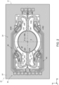
- FIG 2 schematically shows the MEMS device 20, according to an embodiment similar to that shown in Figure 1 and wherein the MEMS device 20 is designed to operate in a dynamic regime (i.e. in resonance, at rotation frequencies of the tiltable structure 22 higher than 10kHz).
- a dynamic regime i.e. in resonance, at rotation frequencies of the tiltable structure 22 higher than 10kHz.
- the MEMS device 20 is formed in the semiconductor body 21 and is provided with the tiltable structure 22.
- the tiltable structure 22 is suspended above the cavity 23 and carries at the top the reflective surface 22' which has, in the illustrated embodiment, a generically circular shape in the plane XY (although other shapes are possible, from an elliptical shape to a polygonal, for example square or rectangular, shape).
- the tiltable structure 22 is elastically coupled to the frame portion 24' of the fixed structure 24 by means of the support structure comprising the first and the second support arms, indicated in Figure 2 with the references 25A, 25B.
- the support arms 25A, 25B extend longitudinally along the first symmetry median axis A, above the cavity 23, between the frame portion 24' of the fixed structure 24 and the tiltable structure 22, on opposite sides thereof.
- the support arms 25A, 25B are equal to each other and arranged symmetrically with respect to the second symmetry median axis C.
- the first support arm 25A has a first end 25A' rigidly coupled to the tiltable structure 22 and a second end 25A" rigidly coupled to the frame portion 24' of the fixed structure 24 and comprises a first and a second torsional spring 27A, 28A.
- the first and the second torsional springs 27A, 28A have a linear shape, extend in continuation with each other along the first symmetry median axis A between a first side of the tiltable structure 22 and a first side of the frame portion 24' of the fixed structure 24.
- the second support arm 25B has a first end 25B' rigidly coupled to the tiltable structure 22 and a second end 25B" rigidly coupled to the frame portion 24' of the fixed structure 24 and comprises a third and a fourth torsional spring 27B, 28B.
- the third and the fourth torsional springs 27B, 28B extend in continuation with each other along the first symmetry median axis A between a second side, opposite to the first, of the tiltable structure 22 and a second side, opposite to the first, of the frame portion 24' of the fixed structure 24.
- the torsional springs 27A, 27B, 28A, 28B each have a linear beam shape rigid for movements outside the plane XY and yielding to torsion around the first symmetry median axis A.
- first and the second torsional springs 27A, 28A are connected to each other at a first constraint structure 29A, that is rigid; in the second support arm 25B, the third and the fourth torsional springs 27B, 28B are connected to each other at a second constraint structure 29B, that is rigid.
- the MEMS device 20 further comprises the plurality of deformable structures 30, in particular at least a first and a second deformable structure 30A1 and 30A2 which extend between the frame portion 24' of the fixed structure 24 and the first constraint structure 29A, on a first and, respectively, a second side of the first support arm 25A, and which have a symmetrical structure with respect to the first symmetry median axis A.
- the first deformable structure 30A1 is coupled to the first constraint structure 29A through a coupling region 35A1 of the first deformable structure 30A1, extending along a main extension direction transverse with respect to a main extension direction of the remaining portion of the first deformable structure 30A1; similarly, the second deformable structure 30A2 is coupled to the first constraint structure 29A through a coupling region 35A2 of the second deformable structure 30A2, which extends along a respective main extension direction transverse with respect to a main extension direction of the remaining portion of the second deformable structure 30A2.
- the plurality of deformable structures 30 further comprises a third and a fourth deformable structure 30B1 and 30B2, extending between the frame portion 24' of the fixed structure 24 and the second constraint structure 29B, on a first and, respectively, a second side of the second support arm 25B.
- the third and the fourth deformable structures 30B1 and 30B2 have a structure symmetrical to each other with respect to the first symmetry median axis A.
- the third deformable structure 30B1 is coupled to the second constraint structure 29B by a coupling region 35B1 of the third deformable structure 30B1, which extends along a respective main extension direction transverse with respect to a main extension direction of the remaining portion of the third deformable structure 30B1; similarly, the fourth deformable structure 30B2 is coupled to the second constraint structure 29B by a coupling region 35B2 of the fourth deformable structure 30B2 which extends along a respective main extension direction transverse with respect to a main extension direction of the remaining portion of the fourth deformable structure 30B2.
- the deformable structures 30A1, 30A2, 30B1 and 30B2 are suspended above the cavity 23 and include, at their top surfaces 30', the respective piezoelectric actuators 38, indicated in more detail in Figure 2 with the respective references 38A1, 38A2, 38B1, 38B2.
- the piezoelectric actuators 38A1, 38A2, 38B1, 38B2 are based on the inverse piezoelectric effect and have a structure which is better discussed hereinbelow.
- the deformable structures 30A1, 30A2, 30B1 include, at their top surfaces 30', the plurality of piezoelectric sensor elements 41. In particular, they comprise the first and the second piezoelectric sensor elements 41A1 and 41A2.
- the first and the second piezoelectric sensor elements 41A1 and 41A2 extend, for example, over the deformable main bodies 31 of the first and, respectively, the second deformable structure 30A1, 30A2 (alternatively and in a manner not shown, they extend over the deformable main bodies 31 of the third and, respectively, the fourth deformable structure 30B1, 30B2).
- the first and the second piezoelectric sensor elements 41A1 and 41A2 extend at the frame portion 24' of the fixed structure 24.
- the plurality of piezoelectric sensor elements further comprises a third and a fourth piezoelectric sensor element 41B1 and 41B2 extending over the deformable main bodies 31 of the third and, respectively, the fourth deformable structure 30B1, 30B2.
- the third and the fourth piezoelectric sensor elements 41B1 and 41B2 extend at the frame portion 24' of the fixed structure 24.
- the third and the fourth piezoelectric sensor elements 41B1 and 41B2 are also present, they may be electrically connected in series to the first and, respectively, the second piezoelectric sensor element 41A1 and 41A2.
- the MEMS device 20 comprises a plurality of electric contact pads 40, which in Figure 2 are exemplarily carried by the frame portion 24' of the fixed structure 24 and electrically connected, by respective lines or vias 43, both to the piezoelectric actuators 38A1, 38A2, 38B1, 38B2, to allow the electrical bias thereof by means of actuation signals coming from the outside of the MEMS device 20, and to the first and the second piezoelectric sensor elements 41A1 and 41A2 (optionally, also to the third and the fourth piezoelectric sensor elements 41B1 and 41B2, if any), to allow the position of the mirror structure to be detected.
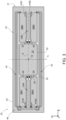
- FIG. 3 schematically shows the MEMS device 20, according to a further embodiment wherein the MEMS device 20 is designed to operate in a quasi-static regime (i.e. at rotation frequencies of the tiltable structure 22 lower than about 200 Hz).
- the deformable structures 30 extend between the frame portion 24' of the fixed structure 24 and the tiltable structure 22, on sides of the latter opposite to each other along the axis X. Therefore, the deformable structures 30 are directly coupled to the tiltable structure 22, and are not instead directly coupled to the support structure as described with reference to Figure 2 .
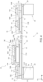
- FIG 4 schematically shows the MEMS device 20 of Figure 1 , with greater details regarding the piezoelectric actuators 38 and the strain sensors 50.
- Figure 4 shows in the plane YZ two deformable structures 30 anchored to the frame portion 24' of the fixed structure 24, suspended on the cavity 23 and respectively facing sides of the tiltable structure 22 which are opposite to each other along the axis Y.
- the tiltable structure 22 is interposed along the axis Y between the two deformable structures 30.
- one of the two deformable structures 30 (e.g., the deformable structure 30 to the left of the tiltable structure 22) has a piezoelectric actuator 38 while the other of the two deformable structures 30 (e.g., the deformable structure 30 to the right of the tiltable structure 22) has a strain sensor 50.
- this is done only for the purpose of simplifying the visualization, the description and the mutual comparison of the piezoelectric sensor elements 41 and the piezoelectric actuators 38, therefore it is not intended in a limiting sense.
- each deformable structure 30 comprises at least one piezoelectric actuator 38 and at least one piezoelectric sensor element 41, arranged side by side to each other; however, showing both these elements for each deformable structure 30 of Figure 4 would have complicated and unnecessarily obscured the representation and understanding of the same Figure.
- Figure 5 shows a similar and more realistic embodiment of the MEMS device 20 wherein a single deformable structure 30 is shown comprising a piezoelectric actuator 38 and a strain sensor 50, extending laterally to each other along the axis Y.
- the piezoelectric actuator 38 extends over the top surface 31' of the deformable main body 31, which is of semiconductor material such as monosilicon or polysilicon and is in particular doped (e.g., with a doping species such as phosphorus) in such a way as to be conductive (e.g., to have electrical resistivity lower than, or equal to, about 30 m ⁇ cm).
- the semiconductor body 21 comprises a double structural layer formed by a SOI (Silicon On Insulator) wafer, therefore it comprises a bottom semiconductive region 21A of semiconductor material such as silicon, an intermediate insulating region 21B of insulating material such as silicon dioxide and a top semiconductive region 21C of semiconductor material such as silicon.
- the piezoelectric actuator 38 comprises an insulating piezoelectric region 51A, of piezoelectric material and in particular of aluminum nitride (AlN) (for example of intrinsic type or doped with one or more doping species such as scandium).
- the insulating piezoelectric region 51A is arranged on the deformable main body 31 so as to electrically insulate it from an active actuation structure 52A of the piezoelectric actuator 38.
- the active actuation structure 52A of the piezoelectric actuator 38 extends over the insulating piezoelectric region 51A and comprises an actuation capacitor 56 formed by an actuation piezoelectric region 61, an intermediate actuation electrode 60A and a top actuation electrode 62A.
- the intermediate actuation electrode 60A is of conductive material, in particular metal material such as platinum, and extends over the insulating piezoelectric region 51A, in contact with the latter.
- the actuation piezoelectric region 61 extends over the intermediate actuation electrode 60A and is formed by piezoelectric material, for example PZT (lead zirconate titanate), BaTiOs, AlN, KNN (sodium potassium niobate), PbTiO 2 or PbNb 2 O 6 .
- the actuation piezoelectric region 61 has a thickness of a few micrometers, for example comprised between 1 um and 3 um.
- the top actuation electrode 62A is of conductive material, in particular a metal material such as platinum or a titanium and tungsten alloy, and extends over the actuation piezoelectric region 61.
- the piezoelectric actuator 38 also comprises a passivation region 64A, of insulating material and with a passivation function.
- the passivation region 64A allows the active actuation structure 52A to be electrically insulated and protected from external contaminants.
- the passivation region 64A is formed here, for example, by a stack of insulating layers.
- this stack of insulating layers comprises a first insulating passivation layer 66A (for example of aluminum oxide or silicon oxide, arranged on the active actuation structure 52A, the insulating piezoelectric region 51A and the deformable main body 31) and a second insulating passivation layer 68A (for example of silicon nitride, SiN, arranged on the first insulating passivation layer 66A).
- the piezoelectric actuator 38 further comprises electrical connections which allow the top actuation electrode 62A, the intermediate actuation electrode 60A and the deformable main body 31 to be electrically controlled, in use.
- the electrical connections of the piezoelectric actuator 38 comprise a first actuation electrical connection 70A in direct physical and electrical coupling with the top actuation electrode 62A, a second actuation electrical connection 70B in direct physical and electrical coupling with the intermediate actuation electrode 60A and a third actuation electrical connection 70C in direct physical and electrical coupling with the top semiconductive region 21C and therefore with the deformable main body 31.
- the second actuation electrical connection 70B and the third electrical connection 70C may be joined into a single actuation electrical connection (in Figures 6A-6R , identified by the reference 70B) in such a way that the intermediate actuation electrode 60A and the top semiconductive region 21C are short-circuited with each other and therefore, in use, at the same electric potential.
- each of these actuation electrical connections 70A-70C comprises a respective connection region 70' and a respective contact pad 70".
- the connection region 70' is formed by a conductive layer, for example of aluminum, AlCu, copper or gold, which extends over at least part of the first insulating passivation layer 66A so as to be exposed from the latter, and which forms a protrusion traversing the first insulating passivation layer 66A and in direct electrical contact with the respective element to be electrically controlled (respectively the top actuation electrode 62A, the intermediate actuation electrode 60A and the deformable main body 31).
- Each contact pad 70" of conductive material such as gold, extends over at least part of the second insulating passivation layer 68A so as to be exposed by the latter, forms a protrusion traversing the second insulating passivation layer 68A and is in direct electrical contact with the respective connection region 70' (therefore, by the latter it is in electrical contact with the respective element to be controlled electrically).
- the contact pads 70" are coupeable in use to an electronic control module (shown in Figure 9 with the reference 92), external to the MEMS device 20 and controllable as better described hereinbelow to bias the piezoelectric actuator 38 and to acquire signals coming from the strain sensor 50, by the contact pads 70" and the connection regions 70'.
- the contact pads 70" and the connection regions 70' may form part of the pads 40 and of the electric lines or vias 43, respectively, or may be independent therefrom.
- the piezoelectric sensor element 41 extends over the top surface 31' of the deformable main body 31.
- the piezoelectric sensor element 41 and the portion of the deformable main body 31 having the piezoelectric sensor element 41 extending thereon together form the strain sensor 50.
- the strain sensor 50 comprises an active detection structure 52B of the strain sensor 50, which is formed by a detection piezoelectric region 51B, a bottom detection electrode and an intermediate detection electrode 60B.
- the deformable main body 31 (in detail, the portion of the deformable main body 31 having the piezoelectric sensor element 41 extending thereon) forms the bottom detection electrode of the active detection structure 52B.
- the detection piezoelectric region 51B is of the same piezoelectric material as the insulating piezoelectric region 51A (in detail AlN) and is arranged on the deformable main body 31, in contact with the latter.
- the intermediate detection electrode 60B is of the same conductive material as the intermediate actuation electrode 60A and extends over the first detection piezoelectric region 51B, in contact with the latter.
- the stack of the deformable main body 31, the first detection piezoelectric region 51B and the intermediate detection electrode 60B forms a first detection capacitor 72' of the active detection structure 52B of the strain sensor 50, which allows the position of the tiltable structure 22 to be detected by measuring the deformation of the deformable structure 30 piezoelectrically, as better described hereinbelow.
- the piezoelectric sensor element 41 further comprises a respective passivation region 64B, similar to the passivation region 64A of the piezoelectric actuator 38.
- the passivation region 64B extends over the active detection structure 52B, over the detection piezoelectric region 51B where exposed by the top detection electrode 62B, and on the deformable main body 31 where exposed by the detection piezoelectric region 51B.
- the passivation region 64B here comprises a respective first insulating passivation layer 66B (similar to the insulating passivation layer 66A and arranged on the active detection structure 52B, the detection piezoelectric region 51B and the deformable main body 31) and a respective second insulating passivation layer 68B (similar to the second insulating passivation layer 68A and arranged on the first insulating passivation layer 66B).
- the piezoelectric sensor element 41 also comprises respective electrical connections which allow in use the active detection structure 52B to be electrically controlled.
- the electrical connections of the piezoelectric sensor element 41 comprise a first detection electrical connection 70D in direct physical and electrical coupling with the intermediate detection electrode 60B and a second detection electrical connection 70E in direct physical and electrical coupling with the top semiconductive region 21C and therefore with the deformable main body 31 which forms the bottom detection electrode of the active detection structure 52B.
- the shape and arrangement of the electrical connections of the piezoelectric sensor element 41 are entirely similar to those of the electrical connections of the piezoelectric actuator 38 and therefore are not described again in detail.
- each piezoelectric actuator 38 is biased, for example by the electronic control module 92, by applying respective bias electric potentials to the top actuation electrode 62A, the intermediate actuation electrode 60A and the deformable main body 31, through the respective actuation electrical connections 70A-70C.
- the intermediate actuation electrode 60A and the deformable main body 31 are set at a same reference electric potential (e.g., at ground, therefore at 0 V) so that the insulating piezoelectric region 51A is not biased and does not actively contribute to the deformation of the deformable structure 30.
- top actuation electrode 62A and the intermediate actuation electrode 60A are biased to different electric potentials and thus a bias electric voltage is applied between the top actuation electrode 62A and the intermediate actuation electrode 60A.
- the application of the bias electric voltage causes, due to the inverse piezoelectric effect, a mechanical deformation of the actuation piezoelectric region 61 of the actuation capacitor 56 and accordingly a deformation of the deformable structure 30, integral therewith.
- each strain sensor 50 generates a respective detection signal (i.e.
- each strain sensor 50 which is linked to the deformation of the deformable structure 30 and therefore to the rotation of the tiltable structure 22 around the rotation axis A.
- the detection electric voltage of each strain sensor 50 is acquired, for example by the electronic control module 92, through the respective detection electrical connections 70D-70E.
- the top semiconductive region 21C of the semiconductor body 21 operates as a bottom electrode for both the piezoelectric actuator 38 (where however it causes no effect on the operation of the piezoelectric actuator 38, since it is set at the same electric potential as the intermediate actuation electrode 60A) and for the strain sensor 50 (where instead it is actively used).
- Controlling the piezoelectric actuators 38, acquiring the detection signals generated by the strain sensors 50 and determining the position of the tiltable structure 22 starting from the acquired detection signals are performed in a per se known manner and not forming part of the present invention, therefore they are not described in detail herein.
- patent document EP4075184 discloses details regarding a differential acquisition of the detection signals of two piezoelectric sensors; nevertheless other types of acquisition are possible, for example single-ended acquisitions.
- the MEMS device 20 may be used by performing an operating method which comprises the following steps: biasing the intermediate actuation electrode 60A and the deformable main body 31 to the reference electric potential; applying a bias electric voltage between the top actuation electrode 62A and the intermediate actuation electrode 60A; and acquiring the first detection electric voltage generated by the strain sensor 50 and indicative of the deformation of the deformable structure 30.
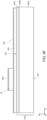
- Figure 6A shows a cross-section of a work wafer 100, in the form of a SOI (Silicon On Insulator) wafer comprising the double structural layer previously described.
- SOI wafer is formed in a per se known manner, for example starting from two wafers of semiconductor material (e.g., silicon) joined to each other at respective oxide layers (e.g., SiO 2 ).
- the work wafer 100 has a first and a second surface 100', 100" opposite to each other along the axis Z, and comprises a bottom semiconductive region 100A of semiconductor material such as silicon, an intermediate insulating region 100B of insulating material such as silicon oxide and a top semiconductive region 100C of semiconductor material such as silicon.
- the bottom semiconductive region 100A and the intermediate insulating region 100B are intended to form the fixed structure 24 which laterally delimits the cavity 23, while the top semiconductive region 100C is intended to form the deformable main body 31.
- the top semiconductive region 100C has the first surface 100' of the work wafer 100, which is therefore intended to form the top surface 31' of the deformable main body 31.
- the top semiconductive region 100C is of doped semiconductor material, such as monosilicon or doped polysilicon (e.g., with a doping species such as phosphorus), in such a way as to be conductive (e.g., to have electrical resistivity lower than, or equal to, about 30 mQ-cm).
- doped semiconductor material such as monosilicon or doped polysilicon (e.g., with a doping species such as phosphorus), in such a way as to be conductive (e.g., to have electrical resistivity lower than, or equal to, about 30 mQ-cm).
- the bottom semiconductive region 100A has a thickness along the axis Z comprised between about 400 um and about 700 um
- the intermediate insulating region 100B has a thickness along the axis Z equal to about 1 um
- the top semiconductive region 100C has a thickness along the axis Z comprised between about 10 um and about 100 um.
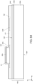
- a first piezoelectric layer 102 of piezoelectric material and in particular of AlN, is formed on the first surface of the work wafer 100, for example having a thickness along the axis Z equal to about 1 um.
- the first piezoelectric layer 102 is intended to form the insulating piezoelectric region 51A of the piezoelectric actuator 38 and the detection piezoelectric region 51B of the strain sensor 50.
- Forming the first piezoelectric layer 102 occurs for example, by deposition, in particular Physical Vapor Deposition (PVD).
- PVD Physical Vapor Deposition
- a first conductive layer 104 of conductive material and in particular of metal material such as platinum, is formed (for example by deposition) on the first piezoelectric layer 102.
- the first conductive layer 104 has a thickness along the axis Z comprised between about 50 nm and about 200 nm.
- the first conductive layer 104 is intended to form the intermediate actuation electrode 60A of the piezoelectric actuator 38 and the intermediate detection electrode 60B of the strain sensor 50.
- a second piezoelectric layer 106 of piezoelectric material such as PZT, for example having a thickness along the axis Z comprised between about 0.5 um and about 3 um, is formed (for example by deposition) on the first conductive layer 104.
- the second piezoelectric layer 106 is intended to form the actuation piezoelectric region 61 of the piezoelectric actuator 38.
- a second conductive layer 108 of conductive material, in particular metal material such as platinum or titanium and tungsten alloy, is formed (for example by deposition), on the second piezoelectric layer 106.
- the second conductive layer 108 has a thickness along the axis Z comprised between about 50 nm and about 200 nm.
- the second conductive layer 108 is intended to form the top actuation electrode 62A of the piezoelectric actuator 38.
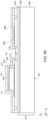
- the first conductive layer 104, the second piezoelectric layer 106 and the second conductive layer 108 form a stack of layers which is patterned ( Figures 6F and 6G ) by means of lithographic steps and selective chemical etchings, known to the person skilled in the art, so that the first conductive layer 104 forms the intermediate actuation electrode 60A of the piezoelectric actuator 38 and the intermediate detection electrode 60B of the strain sensor 50, that the second piezoelectric layer 106 forms the actuation piezoelectric region 61 of the piezoelectric actuator 38 and that the second conductive layer 108 forms the top actuation electrode 62A of the piezoelectric actuator 38.
- the top actuation electrode 62A and the underlying actuation piezoelectric region 61 are patterned in a first etching step and therefore have the same shape.
- a first mask (not shown) is used which covers a region of the second conductive layer 108 adapted to become the top actuation electrode 62A and which exposes the remaining part of the second conductive layer 108.
- the first etching step is performed either by dry etching (for example, plasma-based etching) or wet etching (for example fluorine- or chlorine-based etching), to remove the exposed regions of the second conductive layer 108 and the second piezoelectric layer 106.
- the intermediate actuation electrode 60A of the piezoelectric actuator 38 and the intermediate detection electrode 60B of the strain sensor 50 are patterned in a second etching step, successive to the first etching step.
- a second mask (not shown) is used which covers a first and a second region of the first conductive layer 104 adapted to become the intermediate actuation electrode 60A of the piezoelectric actuator 38 and the intermediate detection electrode 60B of the strain sensor 50, and which exposes the remaining part of the first conductive layer 104; for example, the first region of the first conductive layer 104 adapted to become the intermediate actuation electrode 60A of the piezoelectric actuator 38 is approximately underlying the top actuation electrode 62A and the actuation piezoelectric region 61, while the second region of the first conductive layer 104 adapted to become the intermediate detection electrode 60B of the strain sensor 50 extends laterally to the first region of the first conductive layer 104.
- the second mask (not shown) is used which covers a first and a second region of
- the top actuation electrode 62A, the actuation piezoelectric region 61 and the intermediate actuation electrode 60A therefore form the active actuation structure 52A of the piezoelectric actuator 38.
- a first insulating layer 110 is formed on the active actuation structure 52A of the piezoelectric actuator 38, on the intermediate detection electrode 60B of the strain sensor 50 and on the exposed regions of the first piezoelectric layer 102.
- the first insulating layer 110 is of insulating material such as aluminum oxide or silicon oxide and for example has a thickness along the axis Z comprised between about 100 nm and about 1 um.
- the first insulating layer 110 is intended to form the first insulating passivation layers 66A of the piezoelectric actuator 38 and the strain sensor 50.
- Forming the first insulating layer 110 occurs for example by deposition, in particular Chemical Vapour Deposition (CVD) such as Plasma-Enhanced Chemical Vapor Deposition (PECVD) and/or Atomic Layer Deposition (ALD).
- CVD Chemical Vapour Deposition
- PECVD Plasma-Enhanced Chemical Vapor Deposition
- ALD Atomic Layer Deposition
- first electrical connection openings (or trenches) 112A, 112B and 112C are formed through the first insulating layer 110 in such a way as to partially expose the intermediate detection electrode 60B of the strain sensor 50, the top actuation electrode 62A of the piezoelectric actuator 38 and the intermediate actuation electrode 60A of the piezoelectric actuator 38.
- the first electrical connection openings 112A, 112B and 112C are lateral to each other and are intended to accommodate, at least partially, the connection regions 70' of the electrical connections 70A, 70B and 70D in such a way that they may be in direct electrical contact respectively with the top actuation electrode 62A of the piezoelectric actuator 38, the intermediate actuation electrode 60A of the piezoelectric actuator 38 and the intermediate detection electrode 60B of the strain sensor 50.
- the first electrical connection openings 112A, 112B and 112C are formed by lithographic steps and selective chemical etching, known to the person skilled in the art.
- a third etching step is performed wherein a third mask (not shown) is used which exposes the regions of the first insulating layer 110 to be removed to form the first electrical connection openings 112A, 112B and 112C where the connection regions 70' will be formed, and which covers the remaining parts of the first insulating layer 110.
- the third etching step is performed either by dry etching (for example, plasma-based etching) or wet etching (for example, fluorine-based etching).
- second electrical connection openings (or trenches) 114A, 114B and a first work opening (or trench) 114C are formed which extend through the first insulating layer 110 and the first piezoelectric layer 102 in such a way as to expose regions of the first surface 100' of the work wafer 100.
- the second electrical connection openings 114A, 114B and the first work opening 114C are lateral to each other and with respect to the first electrical connection openings 112A, 112B and 112C.
- the second electrical connection openings 114A, 114B are intended to accommodate, at least partially, the connection regions 70' of the electrical connections 70C and 70E in such a way that they may be in direct electrical contact with the top semiconductive region 100C of the work wafer 100. Instead, the first work opening 114C is intended to expose the portion of the top semiconductive region 100C of the work wafer 100 which will form the tiltable structure 22.
- the second electrical connection openings 114A, 114B and the first work opening 114C are formed by lithographic steps and selective chemical etching, known to the person skilled in the art.
- a fourth etching step is performed wherein a fourth mask (not shown) is used which exposes the regions of the first insulating layer 110 and the underlying regions of the first piezoelectric layer 102 to be removed to form both the second electrical connection openings 114A, 114B (where the connection regions 70' will be formed) and the first work opening 114C (where the tiltable structure 22 will be formed), and which covers the remaining parts of the first insulating layer 110 and the first piezoelectric layer 102.
- the fourth etching step is performed either by dry etching (for example, plasma-based etching) or wet etching (for example, fluorine-based etching).
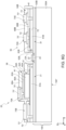
- the portions of the first insulating layer 110 remaining following the etchings of Figures 6I and 6J define the first insulating passivation layers 66A, 66B of the piezoelectric actuator 38 and the strain sensor 50.
- the portions of the first piezoelectric layer 102 remaining following the etchings of Figures 6I and 6J define the insulating piezoelectric region 51A of the piezoelectric actuator 38 and the detection piezoelectric region 51B of the active detection structure 52B of the strain sensor 50, lateral and spaced from each other.
- a third conductive layer 116 is formed on the first insulating passivation layers 66A, 66B of the piezoelectric actuator 38 and the strain sensor 50 and on the exposed regions of the intermediate detection electrode 60B of the strain sensor 50, the top actuation electrode 62A of the piezoelectric actuator 38, the intermediate actuation electrode 60A of the piezoelectric actuator 38 and the top semiconductive region 100C of the work wafer 100.
- the third conductive layer 116 is of conductive material such as aluminum, AlCu, copper or gold and, for example, has a thickness along the axis Z equal to about 0.5 um.
- the third conductive layer 116 is intended to form the connection regions 70' of the electrical connections 70A-70E. Forming the third conductive layer 116 occurs for example by deposition.
- the third conductive layer 116 is patterned by means of lithographic steps and selective chemical etchings, known to the person skilled in the art, in such a way as to form the connection regions 70' of the electrical connections 70A-70E, physically spaced from each other.
- this is done by a fifth etching step and using a fifth mask (not shown) which covers the regions of the third conductive layer 116 adapted to become the connection regions 70' of the electrical connections 70A-70E and which exposes the remaining part of the third conductive layer 116.
- the fifth etching step is performed either by dry etching (for example, plasma-based etching with chlorinated gases) or wet etching (for example, etching based on mixtures of nitric acid and phosphoric acid), to remove the exposed regions of the third conductive layer 116.
- a second insulating layer 118 is formed on the connection regions 70' of the electrical connections 70A-70E, on the first insulating passivation layers 66A, 66B of the piezoelectric actuator 38 and the strain sensor 50 and on the exposed region of the top semiconductive region 100C of the work wafer 100 which will form the tiltable structure 22.
- the second insulating layer 118 is of insulating and passivating material such as SiN and for example has a thickness along the axis Z comprised between about 100 nm and about 1 um.
- the second insulating layer 118 is intended to form the second insulating passivation layers 68A, 68B of the piezoelectric actuator 38 and the strain sensor 50. Forming the second insulating layer 118 occurs for example by deposition (for example CVD).
- the second insulating layer 118 is patterned by means of lithographic steps and selective chemical etchings, known to the person skilled in the art, in such a way as to form the second insulating passivation layers 68A, 68B of the piezoelectric actuator 38 and the strain sensor 50.
- third electrical connection openings (or trenches) 120A-120D and a second work opening (or trench) 120E in the second insulating layer 118.
- the third electrical connection openings 120A-120D extend through the second insulating layer 118 in such a way as to at least partially expose the connection regions 70' of the electrical connections 70A-70E, and are intended to accommodate, at least partially, the contact pads 70" of the electrical connections 70A-70E in such a way that they may be in direct electrical contact with the respective connection regions 70' of the electrical connections 70A-70E.
- the second work opening 120E extends through the second insulating layer 118 in such a way as to expose the portion of the top semiconductive region 100C of the work wafer 100 that will form the tiltable structure 22, therefore is substantially aligned with the first work opening 114C.
- the third electrical connection openings 120A-120D and the second work opening 120E are formed by lithographic steps and selective chemical etching, known to the person skilled in the art.
- a seventh etching step is performed wherein a seventh mask (not shown) is used which exposes the regions of the second insulating layer 118 to be removed to form both the third electrical connection openings 120A-120D (where the contact pads 70" will be formed) and the second work opening 120E (where the tiltable structure 22 will be formed), and which covers the remaining parts of the second insulating layer 118.
- the sixth etching step is performed by dry etching, in particular a plasma-based etching (e.g., a fluorine-based etching).
- the passivation regions 64A and 64B of the piezoelectric actuator 38 and the strain sensor 50 are also formed, as a union of the first insulating passivation layers 66A, 66B and the second insulating passivation layers 68A, 68B.
- the contact pads 70" of the electrical connections 70A-70E are formed in the third electrical connection openings 120A-120D and therefore in direct electrical contact with the connection regions 70' of the electrical connections 70A-70E. This occurs similarly to forming the connection regions 70' of the electrical connections 70A-70E and is therefore not described in detail again.
- a fourth conductive layer (not shown and of a conductive material such as gold, for example with a thickness along the axis Z comprised between about 100 nm and about 500 nm), which is then patterned by means of lithographic steps and selective chemical etchings (known to the person skilled in the art, in particular by an eighth etching step and using an eighth mask) in such a way as to form the contact pads 70" of the electrical connections 70A-70E, physically spaced from each other.
- lithographic steps and selective chemical etchings known to the person skilled in the art, in particular by an eighth etching step and using an eighth mask
- both the strain sensor 50 and the piezoelectric actuator 38 are also formed.
- the reflective surface 22' of the mirror structure is formed on the exposed part of the top semiconductive region 100C of the work wafer 100 which will become the tiltable structure 22. This occurs similarly to forming the connection regions 70' of the electrical connections 70A-70E and therefore it is not described again in detail.
- a fifth conductive layer (not shown and of material reflecting the radiation such as aluminum or gold depending on whether the projection is in the visible or in the infrared), for example with a thickness along the axis Z equal to about 100 nm, which is then patterned by means of lithographic steps and selective chemical etchings (known to the person skilled in the art, in particular by a ninth etching step and using a ninth mask which covers the region of the fifth conductive layer intended to form the reflective surface 22' and which exposes the remaining part of the fifth conductive layer) in such a way as to form the reflective surface 22'.
- a planar profile opening (or trench) 124 is formed through the top semiconductive region 100C of the work wafer 100 and down to reaching the intermediate insulating region 100B of the work wafer 100.
- the planar profile opening 124 physically separates the portions of the top semiconductive region 100C which are intended to form the tiltable structure 22 and the one or more deformable main bodies 31.
- the planar profile opening 124 partially surrounds the deformable main body 31 (i.e., it surrounds the deformable main body 31 except for the portion through which it is intended to be fixed to the fixed structure 24) and completely surrounds the reflective surface 22'.
- the portions of the top semiconductive region 100C underlying the piezoelectric actuator 38 and the piezoelectric sensor element 41 (which will form the deformable main bodies 31) and the portion of the top semiconductive region 100C underlying the reflective surface 22' (which will form the tiltable structure 22) are physically insulated (i.e. spaced) from each other and with respect to the remaining part of the top semiconductive region 100C which will form the fixed structure 24.
- the planar profile opening 124 defines the planar profile, in top view, of the movable parts of the MEMS device 20 which are suspended on the cavity 23.
- the planar profile opening 124 is formed by lithographic steps and selective chemical etching, known to the person skilled in the art.
- a tenth etching step is performed wherein a tenth mask (not shown) is used which exposes the exposed parts of the top semiconductive region 100C, to be removed to form the planar profile opening 124, and which covers the remaining parts of the piezoelectric actuator 38, the strain sensor 50 and the reflective surface 22'.
- the tenth etching step is performed by dry etching, in particular a plasma-based etching, in greater detail a "Deep Reactive Ion Etching", DRIE.
- the cavity 23 is formed to define the mirror structure and the deformable structures 30 of suspended type, and therefore to obtain the MEMS device 20.
- the mirror structure and the deformable structures 30 are suspended on the cavity 23 and the remaining part of the work wafer 100 defines the anchoring structure.
- the cavity 23 is formed by lithographic steps and selective chemical etching, known to the person skilled in the art, starting from the second surface 100" of the work wafer 100 and up to reaching the top semiconductive region 100C.
- this is done by an eleventh etching step wherein an eleventh mask (not shown) is used which exposes the parts of the bottom semiconductive region 100A and the superimposed intermediate insulating region 100B aligned along the axis Z with the piezoelectric actuator 38, the strain sensor 50 and the mirror structure, and which covers the remaining parts of the bottom semiconductive region 100A and the superimposed intermediate insulating region 100B adapted to form the fixed structure 24.
- the eleventh etching step is performed by a selective chemical etching such as a dry chemical etching, for example by dry etching, in particular a plasma-based etching, in greater detail DRIE.
- Figures 6H-6O refer generically to forming the passivation regions 64A, 64B and the electrical connections 70A-70E of the piezoelectric actuator 38 and the strain sensor 50.
- the MEMS device 20 manufactured according to the previously described manufacturing process may be comprised in an electronic apparatus 90, which also comprises the electronic control module 92.
- the electronic control module 92 is operatively coupled to the MEMS device 20 and is configured to acquire the first detection electric voltage, generated by the strain sensor 50 and indicative of the deformation of the deformable structure 30, and electrically control the piezoelectric actuator 38 based on the first detection electric voltage (e.g., in closed- loop), in a per se known manner.
- the MEMS device 20 allows both to actuate a deformation structure piezoelectrically and to monitor its deformation, again piezoelectrically. This allows the position of the tiltable structure 22 to be controlled more accurately.
- the strain sensor 50 is based on AlN and therefore has electrical measurement performances higher than the corresponding known cases based on other piezoelectric materials such as PZT.
- the use of the deformable main body 31 as a bottom detection electrode of the active detection structure 52B allows to actively use (i.e. for detection purposes) an insulating material layer which would in any case be present for known reasons of manufacture and use of the piezoelectric sensors.
- This allows the strain sensor 50 to be formed using a smaller number of manufacturing steps with respect to some known solutions.
- this allows to have the active piezoelectric layers of the piezoelectric actuator 38 and the strain sensor 50 which are of different materials (e.g., PZT for the piezoelectric actuator 38 and AlN for the strain sensor 50) and therefore allows to achieve the simultaneous optimization of both the actuation performances and the detection performances of the MEMS device 20.
- MEMS device 20 is a mirror device, since they allow a mirror device with optimized electrical and use performances to be manufactured at a low cost.
- Figure 7 shows a different embodiment of the MEMS device 20.
- the structure of the MEMS device 20 of Figure 7 is similar to that of the MEMS device 20 of Figure 4 .
- the passivation regions 64A, 64B of the piezoelectric actuator 38 and the strain sensor 50 are monolithic and made entirely of a single material (i.e. they do not comprise a stack of insulating passivation layers), as well as the electrical connections 70A-70E (which for example are entirely of gold). This further simplifies the manufacturing process of the MEMS device 20. Furthermore, the use of gold to form the electrical connections 70A-70E reduces the risk of corrosion of the same in the presence of humidity.
- the passivation regions 64A, 64B of the piezoelectric actuator 38 and the strain sensor 50 are also of AlN, like the insulating piezoelectric region 51A and the detection piezoelectric region 51B.
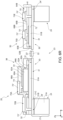
- Figure 8 shows a further embodiment of the MEMS device 20.
- the structure of the MEMS device 20 of Figure 8 is similar to that of the MEMS device 20 of Figure 7 , with the passivation regions 64A, 64B of the piezoelectric actuator 38 and the strain sensor 50 which are monolithic and formed of AlN.
- the strain sensor 50 of the MEMS device 20 of Figure 8 also comprises a top detection electrode 80 which extends over the passivation region 64B of the strain sensor 50, physically spaced from the detection electrical connections 70D-70E and therefore not in direct electrical contact therewith.
- the top detection electrode 80, the intermediate detection electrode 60B and the bottom detection electrode (i.e. the top semiconductive region 21C and therefore with the deformable main body 31) of the active detection structure 52B are superimposed on each other along the axis Z.
- the top detection electrode 80 defines, together with the passivation region 64B of AlN and the intermediate detection electrode 60B, a second detection capacitor 72" of the active detection structure 52B of the strain sensor 50.
- the active detection structure 52B of the strain sensor 50 comprises both the first and the second detection capacitors 72', 72" which share the intermediate detection electrode 60B and which are therefore electrically connected in series with each other.
- the top detection electrode 80 is similar to the intermediate detection electrode 60B and is of conductive material, in particular metal material such as platinum or gold, and extends over the passivation region 64B of AlN 64B, in contact with the latter.
- first and the second detection capacitors 72', 72" in series with each other allows the sensitivity of the measurement of the position of the tiltable structure 22 to be increased without complicating the manufacturing process of the MEMS device 20.
- the top detection electrode 80 may, for example, be formed with the same material as the electrical connections 70A-70E, during the manufacturing of the latter (e.g., manufacturing step of Figure 6L ). Accordingly, no additional masks or manufacturing steps are required since it is sufficient for the fifth mask to also cover the region of the third conductive layer 116 adapted to become the top detection electrode 80.
- the MEMS device 20 is not to be understood as limited to the case of a MEMS mirror device, but may be a generic MEMS device comprising at least one deformable structure 30 actuated piezoelectrically, whose position is desired to be accurately and piezoelectrically detected.
- This deformable structure 30 comprises the respective deformable main body 31 suspended on the cavity and, on the deformable main body 31, at least one piezoelectric sensor element 41 and at least one piezoelectric actuator 38 arranged side by side to each other, similarly to what has been previously described.
- the MEMS device may also be a speaker device, an optical lens device, or a Piezoelectric Micromachined Ultrasonic Transducer (PMUT) device.
- PMUT Piezoelectric Micromachined Ultrasonic Transducer
- the semiconductor body 21 may also be a die of semiconductor material, in particular mono- or polycrystalline silicon.
- the semiconductor body 21 comprises the bottom semiconductive region 21A, of semiconductor material such as silicon and which defines the fixed structure 24 and delimits the cavity 23, and the top semiconductive region 21C, of semiconductor material such as silicon, superimposed on the bottom semiconductive region 21A and which defines the deformable main body 31 suspended on the cavity 23.
- the semiconductor body 21 is formed starting from the work wafer 100 which generally comprises the bottom semiconductive region 100A, of semiconductor material such as silicon and intended to form the fixed structure 24 and to delimit the cavity 23, and the top semiconductive region 100C, of semiconductor material such as silicon, superimposed on the bottom semiconductive region 100A and intended to form the deformable main body 31 suspended on the cavity 23.
Landscapes
- Physics & Mathematics (AREA)
- General Physics & Mathematics (AREA)
- Optics & Photonics (AREA)
- Micromachines (AREA)
Abstract
Description
- The present invention relates to a MEMS device, in particular of mirror type, with improved detection of the deformation of a deformable structure of the same, and manufacturing process of the MEMS device. In particular, it relates to a MEMS device comprising a deformable structure which includes a piezoelectric actuator, for controlling the deformation of the deformable structure, and a strain sensor, for improved detection of the deformation of the deformable structure. It also relates to a manufacturing process of the MEMS device, to an operating method of the MEMS device and to an electronic apparatus comprising the MEMS device.
- As is known, currently micro-electro-mechanical systems (MEMS) devices are commonly used and marketed comprising a tiltable structure, for example a mirror structure, formed with the technology of semiconductor materials.
- For example, MEMS devices having mirror structure are for example used in portable apparatuses, such as portable computers, laptops, notebooks (comprising ultra-thin notebooks), PDAs, tablets, smartphones, for optical applications. In particular, they may be used to direct in desired modes light radiation beams generated by a light source in on-screen or LIDAR-type display applications.
- Thanks to their small size, these devices allow meeting stringent requirements as regards the space occupation, both in terms of area and thickness.
- For example, MEMS mirror devices are used in miniaturized projector modules (so-called picoprojectors), capable of projecting images at a distance or generating desired light patterns.
- MEMS mirror devices generally include a mirror element suspended over a cavity and a deformable structure which elastically couples the mirror element to an anchoring structure of the MEMS mirror device. The mirror element is formed starting from a semiconductor material body in such a way as to be movable, typically with a tilting or rotation movement, to direct the impinging light beam in a desired manner. Generally, the mirror element is controlled and rotated by piezoelectric- or capacitive-type actuators, being part of the deformable structure.
- In order to allow better control of the mirror element and, accordingly, of the light beam directed thereby, it is known to couple one or more strain sensors, configured to detect the deformation of the deformable structure, to the mirror element in order to allow the position of the mirror element to be determined. This allows, for example, the mirror element to be controlled in closed-loop mode, operating the actuators as a function of the detected position of the mirror element. Accordingly, the use of strain sensors allows a more accurate control of the position of the mirror element.
- For this purpose, there is known, for example, using piezoresistive sensors to detect the position of the mirror element. In particular, the piezoresistive sensors comprise sensitive elements of semiconductor material (e.g., silicon) whose electrical resistance is a function of a mechanical deformation of these sensitive elements. Accordingly, when the actuators generate a movement of the mirror element, they also cause the mechanical deformation of the sensitive elements which is detected as a voltage/current variation across the sensitive elements. However, piezoresistive sensors have low measurement sensitivities (e.g., lower than about 3 mV/deg), high electrical consumption, require additional manufacturing steps and therefore higher production costs and times, and are highly dependent on temperature variations (e.g., -0.25%/°C). Because of this, using piezoresistive sensors requires complex calibration procedures to balance the thermal effects to which these sensors may be subject, and in general causes the measurement accuracy to be limited.
- Other known solutions are based on the use of a piezoelectric sensor with "single-ended" reading to detect the position of the mirror element. The piezoelectric sensor comprises a respective sensitive element of piezoelectric insulating material (e.g., lead zirconate-titanate, PZT, or aluminum nitride, AlN) which biases, thus generating a potential difference thereacross, when subject to a mechanical deformation generated by the actuators to control the mirror element. Known solutions comprise reading this potential difference in "single-ended" mode, i.e. amplifying the potential difference, converting it into a respective digital signal by an ADC converter and using this digital signal to determine the position of the mirror element and/or to control the "closed-loop" position thereof.
- Similarly, there are also known solutions based on the use of multiple piezoelectric sensors with differential reading to detect the position of the mirror element. For example, these piezoelectric sensors have a structure similar to that described for the "single-ended" reading case and are arranged symmetrically with respect to the mirror element in such a way as to measure, in use, electrical signals which are in phase-opposition to each other and which therefore may be acquired in differential mode so as to improve the measurement sensitivity and increase the SNR, respectively in the "single-ended" case.
- However, in both cases the piezoelectric sensors are generally formed, laterally to the actuators which are usually of piezoelectric type for easier integration in the manufacturing step with the piezoelectric sensors, or by manufacturing process steps which are additional with respect to those used to form the actuators or by the same manufacturing process steps used to form the actuators.
- In the first case, this entails a greater complexity of the manufacturing process due to the greater number of manufacturing steps and lithographic masks necessary to form the device.
- In the second case, this entails that the strain sensors and the actuators necessarily have similar physical structures (i.e. the vertical succession of the layers which form them is the same for both the strain sensors and the actuators). Furthermore, the piezoelectric insulating material portions used by the actuators to generate the movement of the mirror element and the piezoelectric insulating material portions used by the piezoelectric sensors to detect the movement of the mirror element are part of a same piezoelectric insulating material layer, i.e. are formed starting from the same piezoelectric insulating material (e.g., PZT) layer which is first deposited and then patterned to form the different portions used for the different detection or actuation uses. This generates an additional limit in the device design, as the piezoelectric insulating material used for detecting and actuating is to be the same for both actuators and piezoelectric sensors. This limit is particularly relevant when piezoelectric insulating materials such as PZT are chosen, as this prevents obtaining a device wherein both actuation and detection are optimized. In fact, the PZT is known to become unstable over time due to phenomena such as piezoelectric fatigue and "depoling", which may significantly affect the detection of the position of the mirror element. Furthermore PZT has hysteresis and also has a high dielectric constant (e.g., comprised between about 1000 C2/(N·m2) and about 1200 C2/(N·m2)). Thus, although PZT does not have relevant problems when used for actuation purposes (where the contact areas between PZT and respective electrodes are generally large), this material may be limiting when used for detection purposes (where the contact areas between PZT and respective electrodes are generally reduced) since it may lead to an excessively noisy and inaccurate measurement and to an excessive reduction of the SNR and of the amplitude of the output signal generated by the strain sensor.
- Document
EP 4 075 184 A1 relates to a MEMS device with tiltable structure and improved control. - Document
US 2021/347634 A1 relates to a piezoelectric actuator provided with a deformable structure having improved mechanical properties and to the fabrication method thereof. -
Document CN 108 761 773 A relates to a piezoelectric non-uniform folded beam driven MOEMS scanning grating micromirror, belonging to the field of spectral analysis and micro-optical electromechanical systems. - The aim of the present invention is to provide a MEMS device, a manufacturing process of the MEMS device, an operating method of the MEMS device and an electronic apparatus comprising the MEMS device, which overcome the drawbacks of the prior art.
- According to the present invention there are provided a MEMS device, a manufacturing process of the MEMS device, an operating method of the MEMS device and an electronic apparatus comprising the MEMS device, as defined in the annexed claims.
- For a better understanding of the present invention, a preferred embodiment is now described, purely by way of non-limiting example, with reference to the attached drawings, wherein:
-
Figure 1 schematically represents a lateral sectional view with suspended parts of a MEMS device provided with a tiltable structure and two deformable structures, according to a schematic embodiment; -
Figures 2 and3 are top views of respective embodiments of the MEMS device ofFigure 1 ; -
Figures 4 and5 are lateral sectional views with suspended parts illustrating details of the MEMS device ofFigure 1 , according to respective embodiments; -
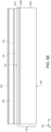
Figures 6A-6R are lateral sectional views illustrating steps of a manufacturing process of the MEMS device ofFigure 1 ; -
Figures 7 and8 are lateral sectional views with suspended parts illustrating details of the MEMS device ofFigure 1 , according to further embodiments; and -
Figure 9 is a block diagram which schematically shows an electronic apparatus comprising the MEMS device ofFigure 1 . - In particular, the Figures are shown with reference to a triaxial Cartesian system defined by an axis X, an axis Y and an axis Z, orthogonal to each other.
- In the following description, elements common to the different embodiments have been indicated with the same reference numerals.
-
Figure 1 schematically shows, in lateral sectional view in a plane YZ defined by the axes Y and Z, aMEMS device 20, in particular a MEMS mirror device. - The
MEMS device 20 is formed in asemiconductor body 21. For example, thesemiconductor body 21 may be a die of semiconductor material, in particular mono- or polycrystalline silicon, or a double structural layer, for example formed by a SOI (Silicon On Insulator) wafer. - The
MEMS device 20 is provided with atiltable structure 22, having main extension in a horizontal plane XY, defined by the axes X and Y, and arranged so as to rotate around a rotation axis A, parallel to the axis X. - The rotation axis A also represents a first symmetry median axis for the
MEMS device 20, therefore also indicated by A; a second symmetry median axis C for theMEMS device 20 is parallel to the axis Y and passing through a center O of thetiltable structure 22. - The
tiltable structure 22 is suspended above acavity 23 formed in thesemiconductor body 21 by afixed structure 24 of thesemiconductor body 21, which delimits thecavity 23. Thetiltable structure 22 carries at the top a reflective surface 22' of theMEMS device 20, so as to define a mirror structure comprising thetiltable structure 22 and the reflective surface 22'. The reflective surface 22' is of material suitable for the application of theMEMS device 20, for example it is of aluminum or gold, depending on whether the projection is in the visible or in the infrared. - The
tiltable structure 22 is elastically coupled to an anchoring structure, here formed by a frame portion 24' of thefixed structure 24, by means of a support structure comprising a first and a second support arm, not shown inFigure 1 because extending longitudinally along the first symmetry median axis A, above thecavity 23, between the frame portion 24' of thefixed structure 24 and thetiltable structure 22, on opposite sides thereof. The support arms are equal to each other and arranged symmetrically with respect to the second symmetry median axis C. - The
MEMS device 20 further comprises a plurality ofdeformable structures 30 which, as shown in greater detail inFigure 2 , extend between thefixed structure 24 of thesemiconductor body 21 and the mirror structure, on sides of the latter opposite to each other along the axis Y and having the respectivedeformable structures 30 facing thereon. In particular, thedeformable structures 30 have a symmetrical structure with respect to the first symmetry median axis A. - The
deformable structures 30 are coupled to the fixedstructure 24 so as to be suspended above thecavity 23. - Each of them comprises a respective deformable
main body 31, which is part of thesemiconductor body 31 and is suspended above thecavity 23. Each deformablemain body 31 is for example of semiconductor material. Each deformablemain body 31 has a respective top surface 31' which is not arranged facing thecavity 23, i.e. which is arranged facing the opposite side of the deformablemain body 31 with respect to thecavity 23. - Furthermore, the deformable
main body 31 has a first and a second end, opposite to each other and not shown. The first end of the deformablemain body 31 is fixed (therefore constrained) to the fixedstructure 24 and the second end of the deformablemain body 31 is fixed to thetiltable structure 22 and is suspended on thecavity 23 so as to be able to move relative to the fixed structure 24 (e.g., so as to be able to oscillate on the cavity 23). - The
deformable structures 30 also include, at their top surfaces 30' (not arranged facing the cavity 23), respective piezoelectric actuators of theMEMS device 20, not shown inFigure 1 but indicated hereinafter with the reference 38 (e.g., as shown inFigure 4 ). Thepiezoelectric actuators 38 are electrically controllable to cause a mechanical deformation of the actuation structures which induces a torsion of the support arms around the first symmetry median axis A and, therefore, a displacement of the mirror structure (in detail, a rotation of thetiltable structure 22 around the first symmetry median axis A). - In particular, each
piezoelectric actuator 38 extends over the top surface 31' of the respective deformablemain body 31, integrally with the deformablemain body 31. Therefore, eachpiezoelectric actuator 38 is arranged facing the opposite side of the deformable main body with respect to thecavity 23. - Furthermore, the
deformable structures 30 also include, at the top surfaces 30', respective piezoelectric sensor elements (indicated inFigure 1 with the references 41A1 and 41A2 and, more generally, with thereference 41 as for example shown inFigure 4 ) . Thepiezoelectric sensor elements 41 form, together with the respective deformablemain bodies 31 whereon they extend,respective strain sensors 50 of piezoelectric type, as better discussed hereinbelow. - In particular, each
piezoelectric sensor element 41 extends on the top surface 31' of the respective deformablemain body 31, integrally with the deformablemain body 31 and so as to also be suspended on thecavity 23. Therefore, eachpiezoelectric sensor element 41 is arranged facing the opposite side of the deformable main body with respect to thecavity 23. - In more detail, the
piezoelectric sensor elements 41 extend symmetrically with respect to the first symmetry median axis A. -
Figure 2 schematically shows theMEMS device 20, according to an embodiment similar to that shown inFigure 1 and wherein theMEMS device 20 is designed to operate in a dynamic regime (i.e. in resonance, at rotation frequencies of thetiltable structure 22 higher than 10kHz). - The
MEMS device 20 is formed in thesemiconductor body 21 and is provided with thetiltable structure 22. - The
tiltable structure 22 is suspended above thecavity 23 and carries at the top the reflective surface 22' which has, in the illustrated embodiment, a generically circular shape in the plane XY (although other shapes are possible, from an elliptical shape to a polygonal, for example square or rectangular, shape). - The
tiltable structure 22 is elastically coupled to the frame portion 24' of the fixedstructure 24 by means of the support structure comprising the first and the second support arms, indicated inFigure 2 with thereferences support arms cavity 23, between the frame portion 24' of the fixedstructure 24 and thetiltable structure 22, on opposite sides thereof. Thesupport arms - In detail, the
first support arm 25A has afirst end 25A' rigidly coupled to thetiltable structure 22 and asecond end 25A" rigidly coupled to the frame portion 24' of the fixedstructure 24 and comprises a first and a secondtorsional spring tiltable structure 22 and a first side of the frame portion 24' of the fixedstructure 24. - The
second support arm 25B has afirst end 25B' rigidly coupled to thetiltable structure 22 and asecond end 25B" rigidly coupled to the frame portion 24' of the fixedstructure 24 and comprises a third and a fourthtorsional spring tiltable structure 22 and a second side, opposite to the first, of the frame portion 24' of the fixedstructure 24. - In detail, the torsional springs 27A, 27B, 28A, 28B each have a linear beam shape rigid for movements outside the plane XY and yielding to torsion around the first symmetry median axis A.
- In the
first support arm 25A, the first and the second torsional springs 27A, 28A are connected to each other at afirst constraint structure 29A, that is rigid; in thesecond support arm 25B, the third and the fourth torsional springs 27B, 28B are connected to each other at asecond constraint structure 29B, that is rigid. - The
MEMS device 20 further comprises the plurality ofdeformable structures 30, in particular at least a first and a second deformable structure 30A1 and 30A2 which extend between the frame portion 24' of the fixedstructure 24 and thefirst constraint structure 29A, on a first and, respectively, a second side of thefirst support arm 25A, and which have a symmetrical structure with respect to the first symmetry median axis A. In detail, the first deformable structure 30A1 is coupled to thefirst constraint structure 29A through a coupling region 35A1 of the first deformable structure 30A1, extending along a main extension direction transverse with respect to a main extension direction of the remaining portion of the first deformable structure 30A1; similarly, the second deformable structure 30A2 is coupled to thefirst constraint structure 29A through a coupling region 35A2 of the second deformable structure 30A2, which extends along a respective main extension direction transverse with respect to a main extension direction of the remaining portion of the second deformable structure 30A2. - In
Figure 2 , the plurality ofdeformable structures 30 further comprises a third and a fourth deformable structure 30B1 and 30B2, extending between the frame portion 24' of the fixedstructure 24 and thesecond constraint structure 29B, on a first and, respectively, a second side of thesecond support arm 25B. The third and the fourth deformable structures 30B1 and 30B2 have a structure symmetrical to each other with respect to the first symmetry median axis A. In detail, the third deformable structure 30B1 is coupled to thesecond constraint structure 29B by a coupling region 35B1 of the third deformable structure 30B1, which extends along a respective main extension direction transverse with respect to a main extension direction of the remaining portion of the third deformable structure 30B1; similarly, the fourth deformable structure 30B2 is coupled to thesecond constraint structure 29B by a coupling region 35B2 of the fourth deformable structure 30B2 which extends along a respective main extension direction transverse with respect to a main extension direction of the remaining portion of the fourth deformable structure 30B2. - The deformable structures 30A1, 30A2, 30B1 and 30B2 are suspended above the
cavity 23 and include, at their top surfaces 30', the respectivepiezoelectric actuators 38, indicated in more detail inFigure 2 with the respective references 38A1, 38A2, 38B1, 38B2. In particular, the piezoelectric actuators 38A1, 38A2, 38B1, 38B2 are based on the inverse piezoelectric effect and have a structure which is better discussed hereinbelow. - Furthermore, the deformable structures 30A1, 30A2, 30B1 include, at their top surfaces 30', the plurality of
piezoelectric sensor elements 41. In particular, they comprise the first and the second piezoelectric sensor elements 41A1 and 41A2. - The first and the second piezoelectric sensor elements 41A1 and 41A2 extend, for example, over the deformable
main bodies 31 of the first and, respectively, the second deformable structure 30A1, 30A2 (alternatively and in a manner not shown, they extend over the deformablemain bodies 31 of the third and, respectively, the fourth deformable structure 30B1, 30B2). By way of non-limiting example, the first and the second piezoelectric sensor elements 41A1 and 41A2 extend at the frame portion 24' of the fixedstructure 24. - Optionally, the plurality of piezoelectric sensor elements further comprises a third and a fourth piezoelectric sensor element 41B1 and 41B2 extending over the deformable
main bodies 31 of the third and, respectively, the fourth deformable structure 30B1, 30B2. For example, the third and the fourth piezoelectric sensor elements 41B1 and 41B2 extend at the frame portion 24' of the fixedstructure 24. In detail, if the third and the fourth piezoelectric sensor elements 41B1 and 41B2 are also present, they may be electrically connected in series to the first and, respectively, the second piezoelectric sensor element 41A1 and 41A2. - Furthermore, optionally the
MEMS device 20 comprises a plurality ofelectric contact pads 40, which inFigure 2 are exemplarily carried by the frame portion 24' of the fixedstructure 24 and electrically connected, by respective lines orvias 43, both to the piezoelectric actuators 38A1, 38A2, 38B1, 38B2, to allow the electrical bias thereof by means of actuation signals coming from the outside of theMEMS device 20, and to the first and the second piezoelectric sensor elements 41A1 and 41A2 (optionally, also to the third and the fourth piezoelectric sensor elements 41B1 and 41B2, if any), to allow the position of the mirror structure to be detected. -
Figure 3 schematically shows theMEMS device 20, according to a further embodiment wherein theMEMS device 20 is designed to operate in a quasi-static regime (i.e. at rotation frequencies of thetiltable structure 22 lower than about 200 Hz). - In particular, the structure of the MEMS device of
Figure 3 is similar to that ofFigure 2 , and therefore it will not be described again in detail herein. - However, in
Figure 3 thedeformable structures 30 extend between the frame portion 24' of the fixedstructure 24 and thetiltable structure 22, on sides of the latter opposite to each other along the axis X. Therefore, thedeformable structures 30 are directly coupled to thetiltable structure 22, and are not instead directly coupled to the support structure as described with reference toFigure 2 . -
Figure 4 schematically shows theMEMS device 20 ofFigure 1 , with greater details regarding thepiezoelectric actuators 38 and thestrain sensors 50. - For purely illustrative and non-limiting purposes,
Figure 4 shows in the plane YZ twodeformable structures 30 anchored to the frame portion 24' of the fixedstructure 24, suspended on thecavity 23 and respectively facing sides of thetiltable structure 22 which are opposite to each other along the axis Y. In other words, thetiltable structure 22 is interposed along the axis Y between the twodeformable structures 30. - Purely by way of example, one of the two deformable structures 30 (e.g., the
deformable structure 30 to the left of the tiltable structure 22) has apiezoelectric actuator 38 while the other of the two deformable structures 30 (e.g., thedeformable structure 30 to the right of the tiltable structure 22) has astrain sensor 50. Nevertheless, this is done only for the purpose of simplifying the visualization, the description and the mutual comparison of thepiezoelectric sensor elements 41 and thepiezoelectric actuators 38, therefore it is not intended in a limiting sense. In fact, in general eachdeformable structure 30 comprises at least onepiezoelectric actuator 38 and at least onepiezoelectric sensor element 41, arranged side by side to each other; however, showing both these elements for eachdeformable structure 30 ofFigure 4 would have complicated and unnecessarily obscured the representation and understanding of the same Figure. - It is therefore evident that the position, the arrangement and the number of the
piezoelectric sensor elements 41 and thepiezoelectric actuators 38 on thedeformable structures 30 may vary with respect to what is shown inFigure 4 , as previously discussed for example with reference toFigures 2 and3 . For example,Figure 5 shows a similar and more realistic embodiment of theMEMS device 20 wherein a singledeformable structure 30 is shown comprising apiezoelectric actuator 38 and astrain sensor 50, extending laterally to each other along the axis Y. - With reference to
Figure 4 , the structures of thepiezoelectric sensor element 41 and thepiezoelectric actuator 38 are shown in detail. - With reference to the
deformable structure 30 ofFigure 4 to the left of thetiltable structure 22, thepiezoelectric actuator 38 extends over the top surface 31' of the deformablemain body 31, which is of semiconductor material such as monosilicon or polysilicon and is in particular doped (e.g., with a doping species such as phosphorus) in such a way as to be conductive (e.g., to have electrical resistivity lower than, or equal to, about 30 mΩ·cm). - For example, in the case of
Figure 4 thesemiconductor body 21 comprises a double structural layer formed by a SOI (Silicon On Insulator) wafer, therefore it comprises a bottomsemiconductive region 21A of semiconductor material such as silicon, an intermediateinsulating region 21B of insulating material such as silicon dioxide and a topsemiconductive region 21C of semiconductor material such as silicon. The bottomsemiconductive region 21A and the intermediateinsulating region 21B laterally delimit thecavity 23 while the topsemiconductive region 21C has a portion which is suspended over thecavity 23 and which forms the deformablemain body 31. - The
piezoelectric actuator 38 comprises an insulatingpiezoelectric region 51A, of piezoelectric material and in particular of aluminum nitride (AlN) (for example of intrinsic type or doped with one or more doping species such as scandium). The insulatingpiezoelectric region 51A is arranged on the deformablemain body 31 so as to electrically insulate it from anactive actuation structure 52A of thepiezoelectric actuator 38. - In the embodiment of
Figure 4 , theactive actuation structure 52A of thepiezoelectric actuator 38 extends over the insulatingpiezoelectric region 51A and comprises anactuation capacitor 56 formed by anactuation piezoelectric region 61, anintermediate actuation electrode 60A and atop actuation electrode 62A. - The
intermediate actuation electrode 60A is of conductive material, in particular metal material such as platinum, and extends over the insulatingpiezoelectric region 51A, in contact with the latter. - The
actuation piezoelectric region 61 extends over theintermediate actuation electrode 60A and is formed by piezoelectric material, for example PZT (lead zirconate titanate), BaTiOs, AlN, KNN (sodium potassium niobate), PbTiO2 or PbNb2O6. For example, theactuation piezoelectric region 61 has a thickness of a few micrometers, for example comprised between 1 um and 3 um. - The
top actuation electrode 62A is of conductive material, in particular a metal material such as platinum or a titanium and tungsten alloy, and extends over theactuation piezoelectric region 61. - The
piezoelectric actuator 38 also comprises apassivation region 64A, of insulating material and with a passivation function. In detail, thepassivation region 64A allows theactive actuation structure 52A to be electrically insulated and protected from external contaminants. - The
passivation region 64A is formed here, for example, by a stack of insulating layers. By way of example, this stack of insulating layers comprises a first insulatingpassivation layer 66A (for example of aluminum oxide or silicon oxide, arranged on theactive actuation structure 52A, the insulatingpiezoelectric region 51A and the deformable main body 31) and a second insulatingpassivation layer 68A (for example of silicon nitride, SiN, arranged on the first insulatingpassivation layer 66A). - The
piezoelectric actuator 38 further comprises electrical connections which allow thetop actuation electrode 62A, theintermediate actuation electrode 60A and the deformablemain body 31 to be electrically controlled, in use. - In detail, the electrical connections of the
piezoelectric actuator 38 comprise a first actuationelectrical connection 70A in direct physical and electrical coupling with thetop actuation electrode 62A, a second actuationelectrical connection 70B in direct physical and electrical coupling with theintermediate actuation electrode 60A and a third actuationelectrical connection 70C in direct physical and electrical coupling with the topsemiconductive region 21C and therefore with the deformablemain body 31. Optionally and as also considered inFigures 6A-6R , the second actuationelectrical connection 70B and the thirdelectrical connection 70C may be joined into a single actuation electrical connection (inFigures 6A-6R , identified by thereference 70B) in such a way that theintermediate actuation electrode 60A and the topsemiconductive region 21C are short-circuited with each other and therefore, in use, at the same electric potential. - For example, each of these actuation
electrical connections 70A-70C comprises a respective connection region 70' and arespective contact pad 70". The connection region 70' is formed by a conductive layer, for example of aluminum, AlCu, copper or gold, which extends over at least part of the first insulatingpassivation layer 66A so as to be exposed from the latter, and which forms a protrusion traversing the first insulatingpassivation layer 66A and in direct electrical contact with the respective element to be electrically controlled (respectively thetop actuation electrode 62A, theintermediate actuation electrode 60A and the deformable main body 31). Eachcontact pad 70", of conductive material such as gold, extends over at least part of the second insulatingpassivation layer 68A so as to be exposed by the latter, forms a protrusion traversing the second insulatingpassivation layer 68A and is in direct electrical contact with the respective connection region 70' (therefore, by the latter it is in electrical contact with the respective element to be controlled electrically). Thecontact pads 70" are coupeable in use to an electronic control module (shown inFigure 9 with the reference 92), external to theMEMS device 20 and controllable as better described hereinbelow to bias thepiezoelectric actuator 38 and to acquire signals coming from thestrain sensor 50, by thecontact pads 70" and the connection regions 70'. For example, thecontact pads 70" and the connection regions 70' may form part of thepads 40 and of the electric lines orvias 43, respectively, or may be independent therefrom. - With reference instead to the
deformable structure 30 ofFigure 4 to the right of thetiltable structure 22, thepiezoelectric sensor element 41 extends over the top surface 31' of the deformablemain body 31. In detail, thepiezoelectric sensor element 41 and the portion of the deformablemain body 31 having thepiezoelectric sensor element 41 extending thereon together form thestrain sensor 50. - The
strain sensor 50 comprises anactive detection structure 52B of thestrain sensor 50, which is formed by adetection piezoelectric region 51B, a bottom detection electrode and anintermediate detection electrode 60B. - The deformable main body 31 (in detail, the portion of the deformable
main body 31 having thepiezoelectric sensor element 41 extending thereon) forms the bottom detection electrode of theactive detection structure 52B. - The
detection piezoelectric region 51B is of the same piezoelectric material as the insulatingpiezoelectric region 51A (in detail AlN) and is arranged on the deformablemain body 31, in contact with the latter. - The
intermediate detection electrode 60B is of the same conductive material as theintermediate actuation electrode 60A and extends over the firstdetection piezoelectric region 51B, in contact with the latter. - Accordingly, the stack of the deformable
main body 31, the firstdetection piezoelectric region 51B and theintermediate detection electrode 60B forms a first detection capacitor 72' of theactive detection structure 52B of thestrain sensor 50, which allows the position of thetiltable structure 22 to be detected by measuring the deformation of thedeformable structure 30 piezoelectrically, as better described hereinbelow. - The
piezoelectric sensor element 41 further comprises arespective passivation region 64B, similar to thepassivation region 64A of thepiezoelectric actuator 38. Thepassivation region 64B extends over theactive detection structure 52B, over thedetection piezoelectric region 51B where exposed by the top detection electrode 62B, and on the deformablemain body 31 where exposed by thedetection piezoelectric region 51B. - Similarly to what has been previously described, the
passivation region 64B here comprises a respective first insulatingpassivation layer 66B (similar to the insulatingpassivation layer 66A and arranged on theactive detection structure 52B, thedetection piezoelectric region 51B and the deformable main body 31) and a respective second insulatingpassivation layer 68B (similar to the second insulatingpassivation layer 68A and arranged on the first insulatingpassivation layer 66B). - In addition to the
detection piezoelectric region 51B, theintermediate detection electrode 60B and thepassivation region 64B, thepiezoelectric sensor element 41 also comprises respective electrical connections which allow in use theactive detection structure 52B to be electrically controlled. - In detail, the electrical connections of the
piezoelectric sensor element 41 comprise a first detectionelectrical connection 70D in direct physical and electrical coupling with theintermediate detection electrode 60B and a second detectionelectrical connection 70E in direct physical and electrical coupling with the topsemiconductive region 21C and therefore with the deformablemain body 31 which forms the bottom detection electrode of theactive detection structure 52B. The shape and arrangement of the electrical connections of thepiezoelectric sensor element 41 are entirely similar to those of the electrical connections of thepiezoelectric actuator 38 and therefore are not described again in detail. - In use, each
piezoelectric actuator 38 is biased, for example by theelectronic control module 92, by applying respective bias electric potentials to thetop actuation electrode 62A, theintermediate actuation electrode 60A and the deformablemain body 31, through the respective actuationelectrical connections 70A-70C. - In particular, the
intermediate actuation electrode 60A and the deformablemain body 31 are set at a same reference electric potential (e.g., at ground, therefore at 0 V) so that the insulatingpiezoelectric region 51A is not biased and does not actively contribute to the deformation of thedeformable structure 30. - Furthermore, the
top actuation electrode 62A and theintermediate actuation electrode 60A are biased to different electric potentials and thus a bias electric voltage is applied between thetop actuation electrode 62A and theintermediate actuation electrode 60A. The application of the bias electric voltage causes, due to the inverse piezoelectric effect, a mechanical deformation of theactuation piezoelectric region 61 of theactuation capacitor 56 and accordingly a deformation of thedeformable structure 30, integral therewith. - Furthermore, the deformations of the
deformable structures 30 caused by the action of thepiezoelectric actuators 38 generate corresponding mechanical deformations in thestrain sensors 50, integral with thedeformable structures 30. Therefore, due to the direct piezoelectric effect, accumulations of charges of opposite sign are generated at the interfaces between the piezoelectric material and the conductive material of the first detection capacitors of theactive detection structures 52B, and then a respective detection electric voltage is generated between theintermediate detection electrode 60B and the bottom detection electrode (the deformable main body 31) of eachactive detection structure 52B. Accordingly, eachstrain sensor 50 generates a respective detection signal (i.e. the detection electric voltage) which is linked to the deformation of thedeformable structure 30 and therefore to the rotation of thetiltable structure 22 around the rotation axis A. The detection electric voltage of eachstrain sensor 50 is acquired, for example by theelectronic control module 92, through the respective detectionelectrical connections 70D-70E. - In other words, the top
semiconductive region 21C of thesemiconductor body 21 operates as a bottom electrode for both the piezoelectric actuator 38 (where however it causes no effect on the operation of thepiezoelectric actuator 38, since it is set at the same electric potential as theintermediate actuation electrode 60A) and for the strain sensor 50 (where instead it is actively used). - Controlling the
piezoelectric actuators 38, acquiring the detection signals generated by thestrain sensors 50 and determining the position of thetiltable structure 22 starting from the acquired detection signals are performed in a per se known manner and not forming part of the present invention, therefore they are not described in detail herein. For example, patent documentEP4075184 discloses details regarding a differential acquisition of the detection signals of two piezoelectric sensors; nevertheless other types of acquisition are possible, for example single-ended acquisitions. - In general, the
MEMS device 20 may be used by performing an operating method which comprises the following steps: biasing theintermediate actuation electrode 60A and the deformablemain body 31 to the reference electric potential; applying a bias electric voltage between thetop actuation electrode 62A and theintermediate actuation electrode 60A; and acquiring the first detection electric voltage generated by thestrain sensor 50 and indicative of the deformation of thedeformable structure 30. - An embodiment of a manufacturing process of the
MEMS device 20 is now described, with reference toFigures 6A-6R which show steps successive to each other of the manufacturing process. - For illustrative and non-limiting example, the steps shown in
Figures 6A-6R refer to the structure shown inFigure 4 . Nonetheless, the steps and considerations made below may similarly be applied to form theMEMS device 20 according to any of the embodiments previously discussed, as evident to the person skilled in the art. -
Figure 6A shows a cross-section of awork wafer 100, in the form of a SOI (Silicon On Insulator) wafer comprising the double structural layer previously described. The SOI wafer is formed in a per se known manner, for example starting from two wafers of semiconductor material (e.g., silicon) joined to each other at respective oxide layers (e.g., SiO2). - The
work wafer 100 has a first and asecond surface 100', 100" opposite to each other along the axis Z, and comprises a bottomsemiconductive region 100A of semiconductor material such as silicon, an intermediateinsulating region 100B of insulating material such as silicon oxide and a topsemiconductive region 100C of semiconductor material such as silicon. The bottomsemiconductive region 100A and the intermediateinsulating region 100B are intended to form the fixedstructure 24 which laterally delimits thecavity 23, while the topsemiconductive region 100C is intended to form the deformablemain body 31. In detail, the topsemiconductive region 100C has the first surface 100' of thework wafer 100, which is therefore intended to form the top surface 31' of the deformablemain body 31. In greater detail, the topsemiconductive region 100C is of doped semiconductor material, such as monosilicon or doped polysilicon (e.g., with a doping species such as phosphorus), in such a way as to be conductive (e.g., to have electrical resistivity lower than, or equal to, about 30 mQ-cm). - For example, the bottom
semiconductive region 100A has a thickness along the axis Z comprised between about 400 um and about 700 um, the intermediateinsulating region 100B has a thickness along the axis Z equal to about 1 um and the topsemiconductive region 100C has a thickness along the axis Z comprised between about 10 um and about 100 um. - With reference to
Figure 6B , a firstpiezoelectric layer 102, of piezoelectric material and in particular of AlN, is formed on the first surface of thework wafer 100, for example having a thickness along the axis Z equal to about 1 um. The firstpiezoelectric layer 102 is intended to form the insulatingpiezoelectric region 51A of thepiezoelectric actuator 38 and thedetection piezoelectric region 51B of thestrain sensor 50. Forming the firstpiezoelectric layer 102 occurs for example, by deposition, in particular Physical Vapor Deposition (PVD). - With reference to
Figure 6C , a firstconductive layer 104, of conductive material and in particular of metal material such as platinum, is formed (for example by deposition) on the firstpiezoelectric layer 102. The firstconductive layer 104 has a thickness along the axis Z comprised between about 50 nm and about 200 nm. The firstconductive layer 104 is intended to form theintermediate actuation electrode 60A of thepiezoelectric actuator 38 and theintermediate detection electrode 60B of thestrain sensor 50. - With reference to
Figure 6D , a secondpiezoelectric layer 106, of piezoelectric material such as PZT, for example having a thickness along the axis Z comprised between about 0.5 um and about 3 um, is formed (for example by deposition) on the firstconductive layer 104. The secondpiezoelectric layer 106 is intended to form theactuation piezoelectric region 61 of thepiezoelectric actuator 38. - With reference to
Figure 6E , a secondconductive layer 108, of conductive material, in particular metal material such as platinum or titanium and tungsten alloy, is formed (for example by deposition), on the secondpiezoelectric layer 106. The secondconductive layer 108 has a thickness along the axis Z comprised between about 50 nm and about 200 nm. The secondconductive layer 108 is intended to form thetop actuation electrode 62A of thepiezoelectric actuator 38. - The first
conductive layer 104, the secondpiezoelectric layer 106 and the secondconductive layer 108 form a stack of layers which is patterned (Figures 6F and6G ) by means of lithographic steps and selective chemical etchings, known to the person skilled in the art, so that the firstconductive layer 104 forms theintermediate actuation electrode 60A of thepiezoelectric actuator 38 and theintermediate detection electrode 60B of thestrain sensor 50, that the secondpiezoelectric layer 106 forms theactuation piezoelectric region 61 of thepiezoelectric actuator 38 and that the secondconductive layer 108 forms thetop actuation electrode 62A of thepiezoelectric actuator 38. - In particular, as visible in
Figure 6F , thetop actuation electrode 62A and the underlyingactuation piezoelectric region 61 are patterned in a first etching step and therefore have the same shape. In detail, during the first etching step a first mask (not shown) is used which covers a region of the secondconductive layer 108 adapted to become thetop actuation electrode 62A and which exposes the remaining part of the secondconductive layer 108. For example, the first etching step is performed either by dry etching (for example, plasma-based etching) or wet etching (for example fluorine- or chlorine-based etching), to remove the exposed regions of the secondconductive layer 108 and the secondpiezoelectric layer 106. - Furthermore, as visible in
Figure 6G , theintermediate actuation electrode 60A of thepiezoelectric actuator 38 and theintermediate detection electrode 60B of thestrain sensor 50 are patterned in a second etching step, successive to the first etching step. In detail, during the second etching step a second mask (not shown) is used which covers a first and a second region of the firstconductive layer 104 adapted to become theintermediate actuation electrode 60A of thepiezoelectric actuator 38 and theintermediate detection electrode 60B of thestrain sensor 50, and which exposes the remaining part of the firstconductive layer 104; for example, the first region of the firstconductive layer 104 adapted to become theintermediate actuation electrode 60A of thepiezoelectric actuator 38 is approximately underlying thetop actuation electrode 62A and theactuation piezoelectric region 61, while the second region of the firstconductive layer 104 adapted to become theintermediate detection electrode 60B of thestrain sensor 50 extends laterally to the first region of the firstconductive layer 104. For example, the second etching step is performed by dry etching, for example a chlorine-based etching, to remove the exposed regions of the firstconductive layer 104. - The
top actuation electrode 62A, theactuation piezoelectric region 61 and theintermediate actuation electrode 60A therefore form theactive actuation structure 52A of thepiezoelectric actuator 38. - With reference to
Figure 6H , a first insulatinglayer 110 is formed on theactive actuation structure 52A of thepiezoelectric actuator 38, on theintermediate detection electrode 60B of thestrain sensor 50 and on the exposed regions of the firstpiezoelectric layer 102. The first insulatinglayer 110 is of insulating material such as aluminum oxide or silicon oxide and for example has a thickness along the axis Z comprised between about 100 nm and about 1 um. The first insulatinglayer 110 is intended to form the first insulatingpassivation layers 66A of thepiezoelectric actuator 38 and thestrain sensor 50. Forming the first insulatinglayer 110 occurs for example by deposition, in particular Chemical Vapour Deposition (CVD) such as Plasma-Enhanced Chemical Vapor Deposition (PECVD) and/or Atomic Layer Deposition (ALD). - With reference to
Figure 6I , first electrical connection openings (or trenches) 112A, 112B and 112C are formed through the first insulatinglayer 110 in such a way as to partially expose theintermediate detection electrode 60B of thestrain sensor 50, thetop actuation electrode 62A of thepiezoelectric actuator 38 and theintermediate actuation electrode 60A of thepiezoelectric actuator 38. The firstelectrical connection openings electrical connections top actuation electrode 62A of thepiezoelectric actuator 38, theintermediate actuation electrode 60A of thepiezoelectric actuator 38 and theintermediate detection electrode 60B of thestrain sensor 50. - The first
electrical connection openings layer 110 to be removed to form the firstelectrical connection openings layer 110. For example, the third etching step is performed either by dry etching (for example, plasma-based etching) or wet etching (for example, fluorine-based etching). - With reference to
Figure 6J , second electrical connection openings (or trenches) 114A, 114B and a first work opening (or trench) 114C are formed which extend through the first insulatinglayer 110 and the firstpiezoelectric layer 102 in such a way as to expose regions of the first surface 100' of thework wafer 100. The secondelectrical connection openings first work opening 114C are lateral to each other and with respect to the firstelectrical connection openings electrical connection openings electrical connections semiconductive region 100C of thework wafer 100. Instead, thefirst work opening 114C is intended to expose the portion of the topsemiconductive region 100C of thework wafer 100 which will form thetiltable structure 22. - The second
electrical connection openings first work opening 114C are formed by lithographic steps and selective chemical etching, known to the person skilled in the art. In particular, a fourth etching step is performed wherein a fourth mask (not shown) is used which exposes the regions of the first insulatinglayer 110 and the underlying regions of the firstpiezoelectric layer 102 to be removed to form both the secondelectrical connection openings first work opening 114C (where thetiltable structure 22 will be formed), and which covers the remaining parts of the first insulatinglayer 110 and the firstpiezoelectric layer 102. For example, the fourth etching step is performed either by dry etching (for example, plasma-based etching) or wet etching (for example, fluorine-based etching). - The portions of the first insulating
layer 110 remaining following the etchings ofFigures 6I and6J define the first insulating passivation layers 66A, 66B of thepiezoelectric actuator 38 and thestrain sensor 50. - Furthermore, the portions of the first
piezoelectric layer 102 remaining following the etchings ofFigures 6I and6J define the insulatingpiezoelectric region 51A of thepiezoelectric actuator 38 and thedetection piezoelectric region 51B of theactive detection structure 52B of thestrain sensor 50, lateral and spaced from each other. - With reference to
Figure 6K , a thirdconductive layer 116 is formed on the first insulating passivation layers 66A, 66B of thepiezoelectric actuator 38 and thestrain sensor 50 and on the exposed regions of theintermediate detection electrode 60B of thestrain sensor 50, thetop actuation electrode 62A of thepiezoelectric actuator 38, theintermediate actuation electrode 60A of thepiezoelectric actuator 38 and the topsemiconductive region 100C of thework wafer 100. The thirdconductive layer 116 is of conductive material such as aluminum, AlCu, copper or gold and, for example, has a thickness along the axis Z equal to about 0.5 um. The thirdconductive layer 116 is intended to form the connection regions 70' of theelectrical connections 70A-70E. Forming the thirdconductive layer 116 occurs for example by deposition. - With reference to
Figure 6L , the thirdconductive layer 116 is patterned by means of lithographic steps and selective chemical etchings, known to the person skilled in the art, in such a way as to form the connection regions 70' of theelectrical connections 70A-70E, physically spaced from each other. - In particular, this is done by a fifth etching step and using a fifth mask (not shown) which covers the regions of the third
conductive layer 116 adapted to become the connection regions 70' of theelectrical connections 70A-70E and which exposes the remaining part of the thirdconductive layer 116. For example, the fifth etching step is performed either by dry etching (for example, plasma-based etching with chlorinated gases) or wet etching (for example, etching based on mixtures of nitric acid and phosphoric acid), to remove the exposed regions of the thirdconductive layer 116. - With reference to
Figure 6M , a second insulatinglayer 118 is formed on the connection regions 70' of theelectrical connections 70A-70E, on the first insulating passivation layers 66A, 66B of thepiezoelectric actuator 38 and thestrain sensor 50 and on the exposed region of the topsemiconductive region 100C of thework wafer 100 which will form thetiltable structure 22. The secondinsulating layer 118 is of insulating and passivating material such as SiN and for example has a thickness along the axis Z comprised between about 100 nm and about 1 um. The secondinsulating layer 118 is intended to form the second insulating passivation layers 68A, 68B of thepiezoelectric actuator 38 and thestrain sensor 50. Forming the second insulatinglayer 118 occurs for example by deposition (for example CVD). - With reference to
Figure 6N , the second insulatinglayer 118 is patterned by means of lithographic steps and selective chemical etchings, known to the person skilled in the art, in such a way as to form the second insulating passivation layers 68A, 68B of thepiezoelectric actuator 38 and thestrain sensor 50. - This occurs by forming third electrical connection openings (or trenches) 120A-120D and a second work opening (or trench) 120E in the second insulating
layer 118. The thirdelectrical connection openings 120A-120D extend through the second insulatinglayer 118 in such a way as to at least partially expose the connection regions 70' of theelectrical connections 70A-70E, and are intended to accommodate, at least partially, thecontact pads 70" of theelectrical connections 70A-70E in such a way that they may be in direct electrical contact with the respective connection regions 70' of theelectrical connections 70A-70E. The second work opening 120E extends through the second insulatinglayer 118 in such a way as to expose the portion of the topsemiconductive region 100C of thework wafer 100 that will form thetiltable structure 22, therefore is substantially aligned with thefirst work opening 114C. - The third
electrical connection openings 120A-120D and the second work opening 120E are formed by lithographic steps and selective chemical etching, known to the person skilled in the art. In particular, a seventh etching step is performed wherein a seventh mask (not shown) is used which exposes the regions of the second insulatinglayer 118 to be removed to form both the thirdelectrical connection openings 120A-120D (where thecontact pads 70" will be formed) and the second work opening 120E (where thetiltable structure 22 will be formed), and which covers the remaining parts of the second insulatinglayer 118. For example, the sixth etching step is performed by dry etching, in particular a plasma-based etching (e.g., a fluorine-based etching). - In this manner, the
passivation regions piezoelectric actuator 38 and thestrain sensor 50 are also formed, as a union of the first insulating passivation layers 66A, 66B and the second insulating passivation layers 68A, 68B. - With reference to
Figure 6O , thecontact pads 70" of theelectrical connections 70A-70E are formed in the thirdelectrical connection openings 120A-120D and therefore in direct electrical contact with the connection regions 70' of theelectrical connections 70A-70E. This occurs similarly to forming the connection regions 70' of theelectrical connections 70A-70E and is therefore not described in detail again. Briefly, there is formed a fourth conductive layer (not shown and of a conductive material such as gold, for example with a thickness along the axis Z comprised between about 100 nm and about 500 nm), which is then patterned by means of lithographic steps and selective chemical etchings (known to the person skilled in the art, in particular by an eighth etching step and using an eighth mask) in such a way as to form thecontact pads 70" of theelectrical connections 70A-70E, physically spaced from each other. - In this manner the
electrical connections 70A-70E are formed. - Accordingly, both the
strain sensor 50 and thepiezoelectric actuator 38 are also formed. - With reference to
Figure 6P , the reflective surface 22' of the mirror structure is formed on the exposed part of the topsemiconductive region 100C of thework wafer 100 which will become thetiltable structure 22. This occurs similarly to forming the connection regions 70' of theelectrical connections 70A-70E and therefore it is not described again in detail. Briefly, there is formed a fifth conductive layer (not shown and of material reflecting the radiation such as aluminum or gold depending on whether the projection is in the visible or in the infrared), for example with a thickness along the axis Z equal to about 100 nm, which is then patterned by means of lithographic steps and selective chemical etchings (known to the person skilled in the art, in particular by a ninth etching step and using a ninth mask which covers the region of the fifth conductive layer intended to form the reflective surface 22' and which exposes the remaining part of the fifth conductive layer) in such a way as to form the reflective surface 22'. - With reference to
Figure 6Q , a planar profile opening (or trench) 124 is formed through the topsemiconductive region 100C of thework wafer 100 and down to reaching the intermediateinsulating region 100B of thework wafer 100. Theplanar profile opening 124 physically separates the portions of the topsemiconductive region 100C which are intended to form thetiltable structure 22 and the one or more deformablemain bodies 31. In other words, in top view and therefore in the plane XY, theplanar profile opening 124 partially surrounds the deformable main body 31 (i.e., it surrounds the deformablemain body 31 except for the portion through which it is intended to be fixed to the fixed structure 24) and completely surrounds the reflective surface 22'. In this manner, the portions of the topsemiconductive region 100C underlying thepiezoelectric actuator 38 and the piezoelectric sensor element 41 (which will form the deformable main bodies 31) and the portion of the topsemiconductive region 100C underlying the reflective surface 22' (which will form the tiltable structure 22) are physically insulated (i.e. spaced) from each other and with respect to the remaining part of the topsemiconductive region 100C which will form the fixedstructure 24. In other words, theplanar profile opening 124 defines the planar profile, in top view, of the movable parts of theMEMS device 20 which are suspended on thecavity 23. - The
planar profile opening 124 is formed by lithographic steps and selective chemical etching, known to the person skilled in the art. In particular, a tenth etching step is performed wherein a tenth mask (not shown) is used which exposes the exposed parts of the topsemiconductive region 100C, to be removed to form theplanar profile opening 124, and which covers the remaining parts of thepiezoelectric actuator 38, thestrain sensor 50 and the reflective surface 22'. For example, the tenth etching step is performed by dry etching, in particular a plasma-based etching, in greater detail a "Deep Reactive Ion Etching", DRIE. - With reference to
Figure 6R , thecavity 23 is formed to define the mirror structure and thedeformable structures 30 of suspended type, and therefore to obtain theMEMS device 20. In fact, after forming thecavity 23, the mirror structure and thedeformable structures 30 are suspended on thecavity 23 and the remaining part of thework wafer 100 defines the anchoring structure. - In particular, the
cavity 23 is formed by lithographic steps and selective chemical etching, known to the person skilled in the art, starting from thesecond surface 100" of thework wafer 100 and up to reaching the topsemiconductive region 100C. In detail, this is done by an eleventh etching step wherein an eleventh mask (not shown) is used which exposes the parts of the bottomsemiconductive region 100A and the superimposed intermediateinsulating region 100B aligned along the axis Z with thepiezoelectric actuator 38, thestrain sensor 50 and the mirror structure, and which covers the remaining parts of the bottomsemiconductive region 100A and the superimposed intermediateinsulating region 100B adapted to form the fixedstructure 24. For example, the eleventh etching step is performed by a selective chemical etching such as a dry chemical etching, for example by dry etching, in particular a plasma-based etching, in greater detail DRIE. - In general, the steps of
Figures 6D-6F refer only to the manufacture of thepiezoelectric actuator 38 and not also to thestrain sensor 50. - Furthermore, the steps of
Figures 6P-6Q (as well as forming thefirst work opening 114C inFigure 6J and the second work opening 120E inFigure 6N ) refer only to the manufacture of the mirror structure. - Furthermore, the steps of
Figures 6H-6O refer generically to forming thepassivation regions electrical connections 70A-70E of thepiezoelectric actuator 38 and thestrain sensor 50. - As shown in
Figure 9 , theMEMS device 20 manufactured according to the previously described manufacturing process may be comprised in anelectronic apparatus 90, which also comprises theelectronic control module 92. Theelectronic control module 92 is operatively coupled to theMEMS device 20 and is configured to acquire the first detection electric voltage, generated by thestrain sensor 50 and indicative of the deformation of thedeformable structure 30, and electrically control thepiezoelectric actuator 38 based on the first detection electric voltage (e.g., in closed- loop), in a per se known manner. - From an examination of the characteristics of the invention made according to the present invention the advantages that it affords are evident.
- In particular, the
MEMS device 20 allows both to actuate a deformation structure piezoelectrically and to monitor its deformation, again piezoelectrically. This allows the position of thetiltable structure 22 to be controlled more accurately. - The
strain sensor 50 is based on AlN and therefore has electrical measurement performances higher than the corresponding known cases based on other piezoelectric materials such as PZT. - Furthermore, the use of the deformable
main body 31 as a bottom detection electrode of theactive detection structure 52B allows to actively use (i.e. for detection purposes) an insulating material layer which would in any case be present for known reasons of manufacture and use of the piezoelectric sensors. This allows thestrain sensor 50 to be formed using a smaller number of manufacturing steps with respect to some known solutions. Furthermore, without the need to increase the number of manufacturing steps with respect to other known solutions, this allows to have the active piezoelectric layers of thepiezoelectric actuator 38 and thestrain sensor 50 which are of different materials (e.g., PZT for thepiezoelectric actuator 38 and AlN for the strain sensor 50) and therefore allows to achieve the simultaneous optimization of both the actuation performances and the detection performances of theMEMS device 20. - These advantages are particularly useful in case the
MEMS device 20 is a mirror device, since they allow a mirror device with optimized electrical and use performances to be manufactured at a low cost. - Finally, it is clear that modifications and variations may be made to the invention described and illustrated herein without thereby departing from the scope of the present invention, as defined in the attached claims. For example, the different embodiments described may be combined with each other so as to provide further solutions.
- Furthermore,
Figure 7 shows a different embodiment of theMEMS device 20. - The structure of the
MEMS device 20 ofFigure 7 is similar to that of theMEMS device 20 ofFigure 4 . - However, in
Figure 7 thepassivation regions piezoelectric actuator 38 and thestrain sensor 50 are monolithic and made entirely of a single material (i.e. they do not comprise a stack of insulating passivation layers), as well as theelectrical connections 70A-70E (which for example are entirely of gold). This further simplifies the manufacturing process of theMEMS device 20. Furthermore, the use of gold to form theelectrical connections 70A-70E reduces the risk of corrosion of the same in the presence of humidity. - Optionally, in
Figure 7 thepassivation regions piezoelectric actuator 38 and thestrain sensor 50 are also of AlN, like the insulatingpiezoelectric region 51A and thedetection piezoelectric region 51B. This improves the mechanical strength of theMEMS device 20 and above all simplifies the manufacturing process of the same and reduces the costs thereof, since fewer materials and fewer steps are required for the manufacturing of the MEMS device 20 (e.g., the thirdconductive layer 116 may be of material such as gold and the manufacturing steps ofFigures 6M-6O may be omitted) . - Furthermore,
Figure 8 shows a further embodiment of theMEMS device 20. - The structure of the
MEMS device 20 ofFigure 8 is similar to that of theMEMS device 20 ofFigure 7 , with thepassivation regions piezoelectric actuator 38 and thestrain sensor 50 which are monolithic and formed of AlN. - Furthermore, the
strain sensor 50 of theMEMS device 20 ofFigure 8 also comprises atop detection electrode 80 which extends over thepassivation region 64B of thestrain sensor 50, physically spaced from the detectionelectrical connections 70D-70E and therefore not in direct electrical contact therewith. In detail, thetop detection electrode 80, theintermediate detection electrode 60B and the bottom detection electrode (i.e. the topsemiconductive region 21C and therefore with the deformable main body 31) of theactive detection structure 52B are superimposed on each other along the axis Z. - The
top detection electrode 80 defines, together with thepassivation region 64B of AlN and theintermediate detection electrode 60B, asecond detection capacitor 72" of theactive detection structure 52B of thestrain sensor 50. In practice, inFigure 8 theactive detection structure 52B of thestrain sensor 50 comprises both the first and thesecond detection capacitors 72', 72" which share theintermediate detection electrode 60B and which are therefore electrically connected in series with each other. - In particular, the
top detection electrode 80 is similar to theintermediate detection electrode 60B and is of conductive material, in particular metal material such as platinum or gold, and extends over thepassivation region 64B ofAlN 64B, in contact with the latter. - The presence of the first and the
second detection capacitors 72', 72" in series with each other allows the sensitivity of the measurement of the position of thetiltable structure 22 to be increased without complicating the manufacturing process of theMEMS device 20. - In fact, the
top detection electrode 80 may, for example, be formed with the same material as theelectrical connections 70A-70E, during the manufacturing of the latter (e.g., manufacturing step ofFigure 6L ). Accordingly, no additional masks or manufacturing steps are required since it is sufficient for the fifth mask to also cover the region of the thirdconductive layer 116 adapted to become thetop detection electrode 80. - In general, the
MEMS device 20 is not to be understood as limited to the case of a MEMS mirror device, but may be a generic MEMS device comprising at least onedeformable structure 30 actuated piezoelectrically, whose position is desired to be accurately and piezoelectrically detected. Thisdeformable structure 30 comprises the respective deformablemain body 31 suspended on the cavity and, on the deformablemain body 31, at least onepiezoelectric sensor element 41 and at least onepiezoelectric actuator 38 arranged side by side to each other, similarly to what has been previously described. For example, the MEMS device may also be a speaker device, an optical lens device, or a Piezoelectric Micromachined Ultrasonic Transducer (PMUT) device. - Furthermore, although the case in which the
semiconductor body 21 is a double structural layer formed by a processed SOI wafer has been previously considered, thesemiconductor body 21 may also be a die of semiconductor material, in particular mono- or polycrystalline silicon. In general, thesemiconductor body 21 comprises the bottomsemiconductive region 21A, of semiconductor material such as silicon and which defines the fixedstructure 24 and delimits thecavity 23, and the topsemiconductive region 21C, of semiconductor material such as silicon, superimposed on the bottomsemiconductive region 21A and which defines the deformablemain body 31 suspended on thecavity 23. Furthermore, thesemiconductor body 21 is formed starting from thework wafer 100 which generally comprises the bottomsemiconductive region 100A, of semiconductor material such as silicon and intended to form the fixedstructure 24 and to delimit thecavity 23, and the topsemiconductive region 100C, of semiconductor material such as silicon, superimposed on the bottomsemiconductive region 100A and intended to form the deformablemain body 31 suspended on thecavity 23.
Claims (16)
- A MEMS device (20) comprising:- a semiconductor body (21) including a fixed structure (24) and a deformable main body (31), the fixed structure (24) defining a cavity (23) in the semiconductor body (21) and the deformable main body (31) being fixed to the fixed structure (24) and suspended on the cavity (23);- a piezoelectric actuator (38) extending over the deformable main body (31); and- a piezoelectric sensor element (41) which extends over the deformable main body (31), laterally to the piezoelectric actuator (38), and which forms with the deformable main body (31) a strain sensor (50),wherein the piezoelectric sensor element (41) comprises:- a detection piezoelectric region (51B) of aluminum nitride, extending over the deformable main body (31); and- an intermediate detection electrode (60B) extending over the detection piezoelectric region (51B),wherein the deformable main body (31), the detection piezoelectric region (51B) and the intermediate detection electrode (60B) form a first detection capacitor (70') of an active detection structure (52B) of the strain sensor (50), the deformable main body (31) being configured to operate as bottom detection electrode of the first detection capacitor (70'),wherein the deformable main body (31), the piezoelectric actuator (38) and the piezoelectric sensor element (41) form a deformable structure (30) suspended on the cavity (23),wherein the piezoelectric actuator (38) is electrically controllable to generate a deformation of the deformable structure (30), andwherein the active detection structure (52B) of the strain sensor (50) is configured to generate, in response to the deformation of the deformable structure (30), a first detection electric voltage between the bottom detection electrode and the intermediate detection electrode (60B) of the first detection capacitor (70'), which is indicative of the deformation of the deformable structure (30).
- The MEMS device (20) according to claim 1, wherein the piezoelectric sensor element (41) further comprises:- a passivation region (64B) of insulating material, extending over the intermediate detection electrode (60B);- a first detection electrical connection (70D) of conductive material, extending through the passivation region (64B) of the piezoelectric sensor element (41) and in electrical contact with the intermediate detection electrode (60B); and- a second detection electrical connection (70E) of conductive material, extending through the passivation region (64B) of the piezoelectric sensor element (41), in electrical contact with the deformable main body (31) and electrically insulated from the first detection electrical connection (70D).
- The MEMS device (20) according to claim 2, wherein the passivation region (64B) is monolithic and is of aluminum nitride.
- The MEMS device (20) according to claim 3, wherein the piezoelectric sensor element (41) further comprises a top detection electrode (80) extending over the passivation region (64B),wherein the top detection electrode (80), the passivation region (64B) and the intermediate detection electrode (60B) form a second detection capacitor (70") of the active detection structure (52B) of the strain sensor (50), the first detection capacitor (70') and the second detection capacitor (70") being electrically in series with each other,wherein the active detection structure (52B) of the strain sensor (50) is further configured to generate, in response to the deformation of the deformable structure (30), a second detection electric voltage between the intermediate detection electrode (60B) and the top detection electrode (80) of the second detection capacitor (70"), which is indicative of the deformation of the deformable structure (30).
- The MEMS device (20) according to any of the preceding claims, wherein the deformable main body (31) is of doped semiconductor material and has an electrical resistivity lower than, or equal to, 30 mΩ·cm.
- The MEMS device (20) according to any of the preceding claims, wherein the piezoelectric actuator (38) includes:- an insulating piezoelectric region (51A) of aluminum nitride, extending over the deformable main body (31) laterally to the detection piezoelectric region (51B);- an intermediate actuation electrode (60A) of conductive material, extending over the insulating piezoelectric region (51A);- an actuation piezoelectric region (61) of piezoelectric material, extending over the intermediate actuation electrode (60A); and- a top actuation electrode (62A) of conductive material, extending over the actuation piezoelectric region (61),wherein the intermediate actuation electrode (60A), the actuation piezoelectric region (61) and the top actuation electrode (62A) form an actuation capacitor (56) of an active actuation structure (52A) of the piezoelectric actuator (38).
- The MEMS device (20) according to claim 6, wherein the piezoelectric actuator (38) further comprises:- a respective passivation region (64A) of insulating material, extending over the top actuation electrode (62A);- a first actuation electrical connection (70A) of conductive material, extending through the passivation region (64A) of the piezoelectric actuator (38) and in electrical contact with the top actuation electrode (62A); and- a second actuation electrical connection (70B) of conductive material, extending through the passivation region (64A) of the piezoelectric actuator (38) and electrically insulated from the first actuation electrical connection (70A), andwherein the second actuation electrical connection (70B) is in electrical contact with the deformable main body (31) and with the intermediate actuation electrode (60A), orwherein the second actuation electrical connection (70B) is in electrical contact with the intermediate actuation electrode (60A) and the piezoelectric actuator (38) further comprises a third actuation electrical connection (70C) of conductive material, which extends through the passivation region (64A) of the piezoelectric actuator (38), is electrically insulated from the first actuation electrical connection (70A) and the second actuation electrical connection (70B) and is in electrical contact with the deformable main body (31).
- The MEMS device (20) according to any of the preceding claims, wherein the MEMS device (20) is of mirror type and further comprises:- a tiltable structure (22) elastically suspended on the cavity (23);- a first and a second support arm (25A, 25B) extending between the fixed structure (24) and opposite sides of the tiltable structure (22), along a rotation axis (A) of the tiltable structure (22);- a plurality of said deformable structures (30) which face opposite sides of the first support arm (25A), extend between the fixed structure (24) and said opposite sides of the first support arm (25A) or between the fixed structure (24) and the tiltable structure (22), and are electrically controllable to deform mechanically thereby generating a rotation of the tiltable structure (22) around the rotation axis (A),wherein the strain sensors (50) of the deformable structures (30) are opposite to each other with respect to the rotation axis (A), andwherein, when the tiltable structure (22) rotates around the rotation axis (A) due to the deformable structures (30), the strain sensors (50) of the deformable structures (30) undergo respective mechanical deformations and generate respective detection signals which are indicative of the rotation of the tiltable structure (22) around the rotation axis (A) and are in phase-opposition to each other.
- A manufacturing process of a MEMS device (20) according to any of claims 1-8, comprising the steps of:a. forming a first piezoelectric layer (102) of aluminum nitride on a first surface (100') of a work wafer (100) comprising a bottom semiconductive region (100A) of semiconductor material and a top semiconductive region (100C) of semiconductor material, superimposed along a first axis (Z) on the bottom semiconductive region (100A) of the work wafer (100) and defining said first surface (100') of the work wafer (100), the work wafer (100) also having a second surface (100") opposite to the first surface (100') along the first axis (Z);b. forming, on the first piezoelectric layer (102), a first conductive layer (104) of conductive material;f. patterning, by chemical etching, the first conductive layer (104) in such a way as to form the intermediate detection electrode (60B) of the strain sensor (50);i. forming, by chemical etching, a first work trench (114C) through the first piezoelectric layer (102) and up to exposing the top semiconductive region (100C) of the work wafer (100), the first work trench (114C) surrounding, orthogonally to the first axis (Z), a portion of the first piezoelectric layer (102) which underlies the intermediate detection electrode (60B) along the first axis (Z) and which forms the detection piezoelectric region (51B);p. forming, by chemical etching, a planar profile trench (124) through the top semiconductive region (100C) of the work wafer (100), the planar profile trench (124) partially surrounding, orthogonally to the first axis (Z), a portion of the top semiconductive region (100C) of the work wafer (100), underlying the detection piezoelectric region (51B) and adapted to form the deformable main body (31), and physically separating, orthogonally to the first axis (Z), part of said portion of the top semiconductive region (100C) from the remaining part of the top semiconductive region (100C) of the work wafer (100) in such a way as to define, orthogonally to the first axis (Z), a planar profile of the deformable main body (31); andq. removing, by chemical etching performed starting from the second surface (100") of the work wafer (100), a portion of the bottom semiconductive region (100A) of the work wafer (100) underlying the deformable main body (31), up to exposing the top semiconductive region (100C) of the work wafer (100), in such a way as to form the cavity (23).
- The manufacturing process of a MEMS device (20) according to claim 9, wherein the piezoelectric actuator (38) includes:- an insulating piezoelectric region (51A) of aluminum nitride, extending over the deformable main body (31) laterally to the detection piezoelectric region (51B);- an intermediate actuation electrode (60A) of conductive material, extending over the insulating piezoelectric region (51A);- an actuation piezoelectric region (61) of piezoelectric material, extending over the intermediate actuation electrode (60A); and- a top actuation electrode (62A) of conductive material, extending over the actuation piezoelectric region (61),wherein the intermediate actuation electrode (60A), the actuation piezoelectric region (61) and the top actuation electrode (62A) form an actuation capacitor (56) of an active actuation structure (52A) of the piezoelectric actuator (38),wherein the manufacturing process further comprises, between steps b and f, the steps of:c. forming, on the first conductive layer (104), a second piezoelectric layer (106) of piezoelectric material;d. forming, on the second piezoelectric layer (106), a second conductive layer (108) of conductive material; ande. patterning, by chemical etching, the second conductive layer (108) and the second piezoelectric layer (106) in such a way as to form, respectively, the top actuation electrode (62A) and the actuation piezoelectric region (61) underlying the top actuation electrode (62A) along the first axis (Z), andwherein step f of patterning the first conductive layer (104) further comprises forming the intermediate actuation electrode (60A) of the piezoelectric actuator (38) laterally to, and spaced from, the intermediate detection electrode (60B) of the strain sensor (50).
- The manufacturing process of a MEMS device (20) according to claim 9 or 10, wherein the piezoelectric sensor element (41) further comprises:- a passivation region (64B) of insulating material, extending over the intermediate detection electrode (60B);- a first detection electrical connection (70D) of conductive material, extending through the passivation region (64B) of the piezoelectric sensor element (41) and in electrical contact with the intermediate detection electrode (60B); and- a second detection electrical connection (70E) of conductive material, extending through the passivation region (64B) of the piezoelectric sensor element (41), in electrical contact with the deformable main body (31) and electrically insulated from the first detection electrical connection (70D), andwherein the manufacturing process further comprises the step of forming the passivation region (64B) on the intermediate detection electrode (60B) and the first detection electrical connection (70D) and the second detection electrical connection (70E) through the passivation region (64B).
- The manufacturing process of a MEMS device (20) according to claim 11, wherein the step of forming the passivation region (64B) on the intermediate detection electrode (60B) and the first detection electrical connection (70D) and the second detection electrical connection (70E) through the passivation region (64B) comprises, between steps f and i, the steps of:g. forming a first insulating layer (110) of insulating material on the intermediate detection electrode (60B) of the strain sensor (50) and on the first piezoelectric layer (102);h. forming a first electrical connection trench (112A) through the first insulating layer (110) in such a way as to partially expose the intermediate detection electrode (60B),wherein step i comprises forming the first work trench (114C) also through the first insulating layer (110), the first work trench (114C) also surrounding, orthogonally to the first axis (Z), a portion of the first insulating layer (110), superimposed on the intermediate detection electrode (60B) along the first axis (Z), which forms a first insulating passivation layer (66B) of the passivation region (64B) of the piezoelectric sensor element (41),wherein step i further comprises forming a second electrical connection trench (114A) through the first insulating layer (110) and the first piezoelectric layer (102) in such a way as to partially expose the top semiconductive region (100C) of the work wafer (100), andwherein the step of forming the passivation region (64B) on the intermediate detection electrode (60B) and the first detection electrical connection (70D) and the second detection electrical connection (70E) through the passivation region (64B) also comprises, between steps i and p, the steps of:j. forming a third conductive layer (116) of conductive material on the first insulating passivation layer (66B) of the passivation region (64B) of the piezoelectric sensor element (41), on the intermediate detection electrode (60B) and on the top semiconductive region (100C) of the work wafer (100);k. patterning, by chemical etching, the third conductive layer (116) in such a way as to form, starting from the third conductive layer (116), a connection region (70') of the first detection electrical connection (70D) in the first electrical connection trench (112A), and a connection region (70') of the second detection electrical connection (70E) in the second electrical connection trench (114A);l. forming a second insulating layer (118) of insulating material on the first insulating passivation layer (66B), the first detection electrical connection (70D) and the second detection electrical connection (70E), the second insulating layer (118) defining a second insulating passivation layer (68B) of the passivation region (64B) of the piezoelectric sensor element (41) and forming together with the first insulating passivation layer (66B) said passivation region (64B) of the piezoelectric sensor element (41) ;m. forming third electrical connection trenches (120A, 120B) through the second insulating layer (118) in such a way as to partially expose the connection regions (70') of the first detection electrical connection (70D) and the second detection electrical connection (70E); andn. forming respective contact pads (70") of the first detection electrical connection (70D) and the second detection electrical connection (70E), of conductive material, in the third electrical connection trenches (120A, 120B) and in electrical contact with the respective connection regions (70'), each contact pad (70") forming with the respective connection region (70') the first detection electrical connection (70D) or, respectively, the second detection electrical connection (70E).
- The manufacturing process of a MEMS device (20) according to claim 11, wherein the piezoelectric sensor element (41) further comprises a top detection electrode (80) extending over the passivation region (64B),wherein the top detection electrode (80), the passivation region (64B) and the intermediate detection electrode (60B) form a second detection capacitor (70") of the active detection structure (52B) of the strain sensor (50), the first detection capacitor (70') and the second detection capacitor (70") being electrically in series with each other,wherein the active detection structure (52B) of the strain sensor (50) is configured to generate, in response to the deformation of the deformable structure (30), a second detection electric voltage between the intermediate detection electrode (60B) and the top detection electrode (80) of the second detection capacitor (70"), which is indicative of the deformation of the deformable structure (30), andwherein the step of forming the passivation region (64B) on the intermediate detection electrode (60B) and the first detection electrical connection (70D) and the second detection electrical connection (70E) through the passivation region (64B) comprises:g. forming a first insulating layer (110) of aluminum nitride on the intermediate detection electrode (60B) of the strain sensor (50) and on the first piezoelectric layer (102);h. forming a first electrical connection trench (112A) through the first insulating layer (110) in such a way as to partially expose the intermediate detection electrode (60B),wherein step i comprises forming the first work trench (114C) also through the first insulating layer (110), the first work trench (114C) also surrounding, orthogonally to the first axis (Z), a portion of the first insulating layer (110), superimposed on the intermediate detection electrode (60B) along the first axis (Z), which forms the passivation region (64B) of the piezoelectric sensor element (41),wherein step i further comprises forming a second electrical connection trench (114A) through the first insulating layer (110) and the first piezoelectric layer (102) in such a way as to partially expose the top semiconductive region (100C) of the work wafer (100), andwherein the step of forming the passivation region (64B) on the intermediate detection electrode (60B) and the first detection electrical connection (70D) and the second detection electrical connection (70E) through the passivation region (64B) further comprises, between steps i and p, the steps of:j. forming a third conductive layer (116) of conductive material on the passivation region (64B) of the piezoelectric sensor element (41), on the intermediate detection electrode (60B) and on the top semiconductive region (100C) of the work wafer (100); andk. patterning, by chemical etching, the third conductive layer (116) in such a way as to form, starting from the third conductive layer (116), the first detection electrical connection (70D) in the first electrical connection trench (112A), the second detection electrical connection (70E) in the second electrical connection trench (114A) and the top detection electrode (80) on the passivation region (64B) of the piezoelectric sensor element (41).
- The manufacturing process of a MEMS device (20) according to any of claims 9-13, wherein the MEMS device (20) is of mirror type, andwherein the manufacturing process further comprises the steps of:- forming a tiltable structure (22) elastically suspended on the cavity (23);- forming a first and a second support arm (25A, 25B) extending between the fixed structure (24) and opposite sides of the tiltable structure (22), along a rotation axis (A) of the tiltable structure (22);- forming a plurality of said deformable structures (30) which face opposite sides of the first support arm (25A), extend between the fixed structure (24) and said opposite sides of the first support arm (25A) or between the fixed structure (24) and the tiltable structure (22), and are electrically controllable to deform mechanically thereby generating a rotation of the tiltable structure (22) around the rotation axis (A),wherein the strain sensors (50) of the deformable structures (30) are opposite to each other with respect to the rotation axis (A),wherein, when the tiltable structure (22) rotates around the rotation axis (A) due to the deformable structures (30), the strain sensors (50) of the deformable structures (30) undergo respective mechanical deformations and generate respective detection signals which are indicative of the rotation of the tiltable structure (22) around the rotation axis (A) and are in phase-opposition to each other.
- An operating method of a MEMS device (20) according to any of claims 1-8, wherein the piezoelectric actuator (38) includes:- an insulating piezoelectric region (51A) of aluminum nitride, extending over the deformable main body (31) laterally to the detection piezoelectric region (51B);- an intermediate actuation electrode (60A) of conductive material, extending over the insulating piezoelectric region (51A);- an actuation piezoelectric region (61) of piezoelectric material, extending over the intermediate actuation electrode (60A); and- a top actuation electrode (62A) of conductive material, extending over the actuation piezoelectric region (61),wherein the intermediate actuation electrode (60A), the actuation piezoelectric region (61) and the top actuation electrode (62A) form an actuation capacitor (56) of an active actuation structure (52A) of the piezoelectric actuator (38),the operating method of the MEMS device (20) comprising the steps of:- biasing the intermediate actuation electrode (60A) and the deformable main body (31) to a reference electric potential;- applying a bias electric voltage between the top actuation electrode (62A) and the intermediate actuation electrode (60A); and- acquiring the first detection electric voltage generated by the strain sensor (50) and indicative of the deformation of the deformable structure (30).
- An electronic apparatus (90) comprising a MEMS device (20), according to any of claims 1-8, and an electronic control module (92) operatively coupled to the MEMS device (20) and configured to acquire the first detection electric voltage, generated by the strain sensor (50) and indicative of the deformation of the deformable structure (30), and electrically control the piezoelectric actuator (38) based on the first detection electric voltage.
Applications Claiming Priority (1)
| Application Number | Priority Date | Filing Date | Title |
|---|---|---|---|
| IT102023000003498A IT202300003498A1 (en) | 2023-02-27 | 2023-02-27 | MEMS DEVICE, ESPECIALLY OF THE MIRROR TYPE, WITH IMPROVED DETECTION OF THE DEFORMABLE STRUCTURE OF THE SAME, AND MANUFACTURING PROCESS OF THE MEMS DEVICE |
Publications (2)
| Publication Number | Publication Date |
|---|---|
| EP4421551A1 true EP4421551A1 (en) | 2024-08-28 |
| EP4421551B1 EP4421551B1 (en) | 2025-11-26 |
Family
ID=86099775
Family Applications (1)
| Application Number | Title | Priority Date | Filing Date |
|---|---|---|---|
| EP24156497.0A Active EP4421551B1 (en) | 2023-02-27 | 2024-02-08 | Mems device, in particular of mirror type, with improved detection of the deformation of a deformable structure of the same, and manufacturing process of the mems device |
Country Status (3)
| Country | Link |
|---|---|
| US (1) | US20240288680A1 (en) |
| EP (1) | EP4421551B1 (en) |
| IT (1) | IT202300003498A1 (en) |
Families Citing this family (1)
| Publication number | Priority date | Publication date | Assignee | Title |
|---|---|---|---|---|
| JP2026065489A (en) * | 2024-10-03 | 2026-04-15 | スタンレー電気株式会社 | Displacement measuring device and optical deflector |
Citations (3)
| Publication number | Priority date | Publication date | Assignee | Title |
|---|---|---|---|---|
| CN108761773A (en) | 2018-06-15 | 2018-11-06 | 重庆大学 | A kind of MOEMS raster micro mirrors of the non-homogeneous folded beam driving of piezoelectricity |
| US20210347634A1 (en) | 2020-05-07 | 2021-11-11 | Stmicroelectronics S.R.L. | Piezoelectric actuator provided with a deformable structure having improved mechanical properties and fabrication method thereof |
| EP4075184A1 (en) | 2021-04-16 | 2022-10-19 | STMicroelectronics S.r.l. | Mems device with tiltable structure and improved control |
-
2023
- 2023-02-27 IT IT102023000003498A patent/IT202300003498A1/en unknown
-
2024
- 2024-02-08 EP EP24156497.0A patent/EP4421551B1/en active Active
- 2024-02-22 US US18/584,533 patent/US20240288680A1/en active Pending
Patent Citations (3)
| Publication number | Priority date | Publication date | Assignee | Title |
|---|---|---|---|---|
| CN108761773A (en) | 2018-06-15 | 2018-11-06 | 重庆大学 | A kind of MOEMS raster micro mirrors of the non-homogeneous folded beam driving of piezoelectricity |
| US20210347634A1 (en) | 2020-05-07 | 2021-11-11 | Stmicroelectronics S.R.L. | Piezoelectric actuator provided with a deformable structure having improved mechanical properties and fabrication method thereof |
| EP4075184A1 (en) | 2021-04-16 | 2022-10-19 | STMicroelectronics S.r.l. | Mems device with tiltable structure and improved control |
Also Published As
| Publication number | Publication date |
|---|---|
| EP4421551B1 (en) | 2025-11-26 |
| IT202300003498A1 (en) | 2024-08-27 |
| US20240288680A1 (en) | 2024-08-29 |
Similar Documents
| Publication | Publication Date | Title |
|---|---|---|
| US11623246B2 (en) | Piezoelectric micromachined ultrasound transducer device with piezoelectric barrier layer | |
| US11350218B2 (en) | Piezoelectric microelectromechanical acoustic transducer having improved characteristics and corresponding manufacturing process | |
| Wang et al. | Design, fabrication, and measurement of high-sensitivity piezoelectric microelectromechanical systems accelerometers | |
| US8004154B2 (en) | Piezoelectric actuation structure including an integrated piezoresistive strain gauge and its production method | |
| CN108017036B (en) | Piezoelectric MEMS sensor with improved sensitivity, such as a force, pressure, deformation sensor or microphone | |
| JP4600468B2 (en) | SEMICONDUCTOR PRESSURE SENSOR AND ITS MANUFACTURING METHOD, SEMICONDUCTOR DEVICE, AND ELECTRONIC DEVICE | |
| CN105405961B (en) | Piezoelectric position sensor for piezoelectrically driven resonant micromirrors | |
| JP5309898B2 (en) | Pressure sensor device | |
| US20160002026A1 (en) | Methods and devices for microelectromechanical pressure sensors | |
| US20060284516A1 (en) | Microphone and a method of manufacturing a microphone | |
| US10495514B2 (en) | Mirror plate for a fabry-perot interferometer and a fabry-perot interferometer | |
| WO2007037926A2 (en) | Mems pixel sensor | |
| EP4421551B1 (en) | Mems device, in particular of mirror type, with improved detection of the deformation of a deformable structure of the same, and manufacturing process of the mems device | |
| Sadeghpour et al. | Flexible soi-based piezoelectric micromachined ultrasound transducer (PMUT) arrays | |
| JPH1022509A (en) | Sensor device | |
| EP4075184B1 (en) | Electronic apparatus comprising a mems device with tiltable structure and improved control | |
| CN112563405B (en) | Pressure sensor unit, multi-dimensional pressure sensor and method for manufacturing the same | |
| US11600765B2 (en) | Piezoelectric actuator having a deformation sensor and fabrication method thereof | |
| CN118545673A (en) | MEMS device and manufacturing process thereof | |
| JP6424337B2 (en) | Tunable optical filter module | |
| US20240328879A1 (en) | A multi-axis force sensor | |
| WO2026075233A1 (en) | Displacement measurement device and optical deflector | |
| US20250248308A1 (en) | Piezoelectric device, ultrasonic transducer, micro-electromechanical device and method of forming a piezoelectric device | |
| JP6594527B2 (en) | Compound sensor | |
| CN120943207A (en) | A monolithic integrated chip and its fabrication method |
Legal Events
| Date | Code | Title | Description |
|---|---|---|---|
| PUAI | Public reference made under article 153(3) epc to a published international application that has entered the european phase |
Free format text: ORIGINAL CODE: 0009012 |
|
| STAA | Information on the status of an ep patent application or granted ep patent |
Free format text: STATUS: THE APPLICATION HAS BEEN PUBLISHED |
|
| AK | Designated contracting states |
Kind code of ref document: A1 Designated state(s): AL AT BE BG CH CY CZ DE DK EE ES FI FR GB GR HR HU IE IS IT LI LT LU LV MC ME MK MT NL NO PL PT RO RS SE SI SK SM TR |
|
| STAA | Information on the status of an ep patent application or granted ep patent |
Free format text: STATUS: REQUEST FOR EXAMINATION WAS MADE |
|
| 17P | Request for examination filed |
Effective date: 20250219 |
|
| GRAP | Despatch of communication of intention to grant a patent |
Free format text: ORIGINAL CODE: EPIDOSNIGR1 |
|
| STAA | Information on the status of an ep patent application or granted ep patent |
Free format text: STATUS: GRANT OF PATENT IS INTENDED |
|
| INTG | Intention to grant announced |
Effective date: 20250627 |
|
| GRAS | Grant fee paid |
Free format text: ORIGINAL CODE: EPIDOSNIGR3 |
|
| GRAA | (expected) grant |
Free format text: ORIGINAL CODE: 0009210 |
|
| STAA | Information on the status of an ep patent application or granted ep patent |
Free format text: STATUS: THE PATENT HAS BEEN GRANTED |
|
| AK | Designated contracting states |
Kind code of ref document: B1 Designated state(s): AL AT BE BG CH CY CZ DE DK EE ES FI FR GB GR HR HU IE IS IT LI LT LU LV MC ME MK MT NL NO PL PT RO RS SE SI SK SM TR |
|
| REG | Reference to a national code |
Ref country code: CH Ref legal event code: F10 Free format text: ST27 STATUS EVENT CODE: U-0-0-F10-F00 (AS PROVIDED BY THE NATIONAL OFFICE) Effective date: 20251126 Ref country code: GB Ref legal event code: FG4D |
|
| REG | Reference to a national code |
Ref country code: IE Ref legal event code: FG4D |
|
| REG | Reference to a national code |
Ref country code: DE Ref legal event code: R096 Ref document number: 602024001352 Country of ref document: DE |
|
| REG | Reference to a national code |
Ref country code: NL Ref legal event code: MP Effective date: 20251126 |
|
| PG25 | Lapsed in a contracting state [announced via postgrant information from national office to epo] |
Ref country code: ES Free format text: LAPSE BECAUSE OF FAILURE TO SUBMIT A TRANSLATION OF THE DESCRIPTION OR TO PAY THE FEE WITHIN THE PRESCRIBED TIME-LIMIT Effective date: 20251126 |
|
| REG | Reference to a national code |
Ref country code: LT Ref legal event code: MG9D |
|
| PG25 | Lapsed in a contracting state [announced via postgrant information from national office to epo] |
Ref country code: NO Free format text: LAPSE BECAUSE OF FAILURE TO SUBMIT A TRANSLATION OF THE DESCRIPTION OR TO PAY THE FEE WITHIN THE PRESCRIBED TIME-LIMIT Effective date: 20260226 |
|
| PGFP | Annual fee paid to national office [announced via postgrant information from national office to epo] |
Ref country code: DE Payment date: 20260121 Year of fee payment: 3 |
|
| PG25 | Lapsed in a contracting state [announced via postgrant information from national office to epo] |
Ref country code: FI Free format text: LAPSE BECAUSE OF FAILURE TO SUBMIT A TRANSLATION OF THE DESCRIPTION OR TO PAY THE FEE WITHIN THE PRESCRIBED TIME-LIMIT Effective date: 20251126 Ref country code: AT Free format text: LAPSE BECAUSE OF FAILURE TO SUBMIT A TRANSLATION OF THE DESCRIPTION OR TO PAY THE FEE WITHIN THE PRESCRIBED TIME-LIMIT Effective date: 20251126 Ref country code: HR Free format text: LAPSE BECAUSE OF FAILURE TO SUBMIT A TRANSLATION OF THE DESCRIPTION OR TO PAY THE FEE WITHIN THE PRESCRIBED TIME-LIMIT Effective date: 20251126 |
|
| PGFP | Annual fee paid to national office [announced via postgrant information from national office to epo] |
Ref country code: AT Payment date: 20260301 Year of fee payment: 3 |
|
| REG | Reference to a national code |
Ref country code: AT Ref legal event code: MK05 Ref document number: 1861614 Country of ref document: AT Kind code of ref document: T Effective date: 20251126 |
|
| PG25 | Lapsed in a contracting state [announced via postgrant information from national office to epo] |
Ref country code: NL Free format text: LAPSE BECAUSE OF FAILURE TO SUBMIT A TRANSLATION OF THE DESCRIPTION OR TO PAY THE FEE WITHIN THE PRESCRIBED TIME-LIMIT Effective date: 20251126 |
|
| PG25 | Lapsed in a contracting state [announced via postgrant information from national office to epo] |
Ref country code: RS Free format text: LAPSE BECAUSE OF FAILURE TO SUBMIT A TRANSLATION OF THE DESCRIPTION OR TO PAY THE FEE WITHIN THE PRESCRIBED TIME-LIMIT Effective date: 20260226 |
|
| PG25 | Lapsed in a contracting state [announced via postgrant information from national office to epo] |
Ref country code: IS Free format text: LAPSE BECAUSE OF FAILURE TO SUBMIT A TRANSLATION OF THE DESCRIPTION OR TO PAY THE FEE WITHIN THE PRESCRIBED TIME-LIMIT Effective date: 20260326 |
|
| PG25 | Lapsed in a contracting state [announced via postgrant information from national office to epo] |
Ref country code: PT Free format text: LAPSE BECAUSE OF FAILURE TO SUBMIT A TRANSLATION OF THE DESCRIPTION OR TO PAY THE FEE WITHIN THE PRESCRIBED TIME-LIMIT Effective date: 20260326 |
|
| PG25 | Lapsed in a contracting state [announced via postgrant information from national office to epo] |
Ref country code: PL Free format text: LAPSE BECAUSE OF FAILURE TO SUBMIT A TRANSLATION OF THE DESCRIPTION OR TO PAY THE FEE WITHIN THE PRESCRIBED TIME-LIMIT Effective date: 20251126 |
|
| PG25 | Lapsed in a contracting state [announced via postgrant information from national office to epo] |
Ref country code: LV Free format text: LAPSE BECAUSE OF FAILURE TO SUBMIT A TRANSLATION OF THE DESCRIPTION OR TO PAY THE FEE WITHIN THE PRESCRIBED TIME-LIMIT Effective date: 20251126 |