EP4075184A1 - Mems device with tiltable structure and improved control - Google Patents
Mems device with tiltable structure and improved control Download PDFInfo
- Publication number
- EP4075184A1 EP4075184A1 EP22167952.5A EP22167952A EP4075184A1 EP 4075184 A1 EP4075184 A1 EP 4075184A1 EP 22167952 A EP22167952 A EP 22167952A EP 4075184 A1 EP4075184 A1 EP 4075184A1
- Authority
- EP
- European Patent Office
- Prior art keywords
- piezoelectric
- mems device
- rotation axis
- differential
- tiltable structure
- Prior art date
- Legal status (The legal status is an assumption and is not a legal conclusion. Google has not performed a legal analysis and makes no representation as to the accuracy of the status listed.)
- Granted
Links
Images



Classifications
-
- B—PERFORMING OPERATIONS; TRANSPORTING
- B81—MICROSTRUCTURAL TECHNOLOGY
- B81B—MICROSTRUCTURAL DEVICES OR SYSTEMS, e.g. MICROMECHANICAL DEVICES
- B81B5/00—Devices comprising elements which are movable in relation to each other, e.g. comprising slidable or rotatable elements
-
- B—PERFORMING OPERATIONS; TRANSPORTING
- B81—MICROSTRUCTURAL TECHNOLOGY
- B81B—MICROSTRUCTURAL DEVICES OR SYSTEMS, e.g. MICROMECHANICAL DEVICES
- B81B7/00—Microstructural systems ; Auxiliary parts of microstructural devices or systems
- B81B7/02—Microstructural systems ; Auxiliary parts of microstructural devices or systems containing distinct electrical or optical devices of particular relevance for their function, e.g. microelectro-mechanical systems [MEMS]
-
- G—PHYSICS
- G02—OPTICS
- G02B—OPTICAL ELEMENTS, SYSTEMS OR APPARATUS
- G02B26/00—Optical devices or arrangements for the control of light using movable or deformable optical elements
- G02B26/08—Optical devices or arrangements for the control of light using movable or deformable optical elements for controlling the direction of light
- G02B26/0816—Optical devices or arrangements for the control of light using movable or deformable optical elements for controlling the direction of light by means of one or more reflecting elements
- G02B26/0833—Optical devices or arrangements for the control of light using movable or deformable optical elements for controlling the direction of light by means of one or more reflecting elements the reflecting element being a micromechanical device, e.g. a MEMS mirror, DMD
- G02B26/0858—Optical devices or arrangements for the control of light using movable or deformable optical elements for controlling the direction of light by means of one or more reflecting elements the reflecting element being a micromechanical device, e.g. a MEMS mirror, DMD the reflecting means being moved or deformed by piezoelectric means
-
- H—ELECTRICITY
- H02—GENERATION; CONVERSION OR DISTRIBUTION OF ELECTRIC POWER
- H02N—ELECTRIC MACHINES NOT OTHERWISE PROVIDED FOR
- H02N2/00—Electric machines in general using piezoelectric effect, electrostriction or magnetostriction
- H02N2/02—Electric machines in general using piezoelectric effect, electrostriction or magnetostriction producing linear motion, e.g. actuators; Linear positioners ; Linear motors
- H02N2/028—Electric machines in general using piezoelectric effect, electrostriction or magnetostriction producing linear motion, e.g. actuators; Linear positioners ; Linear motors along multiple or arbitrary translation directions, e.g. XYZ stages
-
- H—ELECTRICITY
- H02—GENERATION; CONVERSION OR DISTRIBUTION OF ELECTRIC POWER
- H02N—ELECTRIC MACHINES NOT OTHERWISE PROVIDED FOR
- H02N2/00—Electric machines in general using piezoelectric effect, electrostriction or magnetostriction
- H02N2/02—Electric machines in general using piezoelectric effect, electrostriction or magnetostriction producing linear motion, e.g. actuators; Linear positioners ; Linear motors
- H02N2/06—Drive circuits; Control arrangements or methods
- H02N2/062—Small signal circuits; Means for controlling position or derived quantities, e.g. for removing hysteresis
-
- B—PERFORMING OPERATIONS; TRANSPORTING
- B81—MICROSTRUCTURAL TECHNOLOGY
- B81B—MICROSTRUCTURAL DEVICES OR SYSTEMS, e.g. MICROMECHANICAL DEVICES
- B81B2201/00—Specific applications of microelectromechanical systems
- B81B2201/04—Optical MEMS
- B81B2201/042—Micromirrors, not used as optical switches
Definitions
- the present invention relates to a MEMS device with tiltable structure and improved control.
- the present invention relates to a MEMS device, an electronic apparatus comprising the MEMS device and a method of using the MEMS device and, in greater detail, to a micro-mirror having the tiltable structure piezoelectrically controlled, comprising piezoelectric sensors configured to sense sensing signals in phase opposition to each other and acquired in a differential manner.
- MEMS devices having a mirror structure made using the semiconductor material technology.
- MEMS devices are for example used in portable apparatuses, such as portable computers, laptops, notebooks (including ultra-thin notebooks), PDAs, tablets, smartphones, for optical applications, in particular to direct light radiation beams generated by a light source in on-screen or LIDAR-type display applications in desired manners.
- portable apparatuses such as portable computers, laptops, notebooks (including ultra-thin notebooks), PDAs, tablets, smartphones, for optical applications, in particular to direct light radiation beams generated by a light source in on-screen or LIDAR-type display applications in desired manners.
- micro-electro-mechanical mirror devices are used in miniaturized projectors modules (so-called picoprojectors), capable of projecting images from a distance or generating desired light patterns.
- picoprojectors miniaturized projectors modules
- Micro-electro-mechanical mirror devices generally include a mirror element suspended on a cavity and made from a body of semiconductor material so as to be movable, typically with tilt or rotation movement, to direct the incident light beam in a desired manner.
- the mirror element is controlled and rotated by actuators of piezoelectric or capacitive type.
- piezoresistive sensors comprise sensing elements of semiconductor material (e.g., silicon) whose electrical resistance is a function of a mechanical deformation of these sensing elements.
- semiconductor material e.g., silicon
- the piezoresistive sensors have reduced measure sensitivities (e.g., lower than approximately 3 mV/deg), require additional manufacturing steps and therefore higher production costs and times, and are highly dependent on temperature variations (e.g., - 0.25%/°C). Because of this, the use of piezoresistive sensors requires complex calibration procedures to balance the thermal effects to which these sensors may be subject, and in general causes measurement accuracy to be limited.
- the piezoelectric sensor comprises a respective sensing element of insulating material (e.g., lead zirconate titanate, PZT, or aluminum nitride, AlN) which biases, thus generating a potential difference thereacross, when subject to a mechanical deformation generated by the actuators to control the mirror element.
- the known solutions comprise acquiring this potential difference in single-ended mode, that is, amplifying the potential difference, converting it into a respective digital signal through an ADC converter and using this digital signal to determine the position of the mirror element and/or to control the position in closed-loop.
- the digital signal thus obtained is sensitive to mechanical modes of the MEMS device and is dependent on electrical disturbances and measurement noise, and therefore this type of sensing has a reduced signal-to-noise ratio.
- Document CN 108 761 773 A relates to a piezoelectric non-uniform folded beam driven MOEMS scanning grating micromirror, belonging to the field of spectral analysis and micro-optical electromechanical systems.
- Document EP 3 715 317 A1 relates to a resonant MEMS (Micro-Electro-Mechanical System) device having a tiltable, piezoelectrically controlled structure, in particular a micromirror.
- MEMS Micro-Electro-Mechanical System
- the aim of the present invention is to provide a MEMS device, an electronic apparatus comprising the MEMS device and a method of using the MEMS device, which overcome the drawbacks of the prior art.
- a MEMS device an electronic apparatus comprising the MEMS device and a method of using the MEMS device are provided, as defined in the annexed claims.
- Figure 1 schematically shows, in a lateral crosssection view in a Cartesian (triaxial) reference system of axes X, Y, Z, a MEMS device 20, in particular a mirror device.
- the MEMS device 20 is formed in a semiconductor body 21.
- the semiconductor body 21 may be a die of semiconductor material, in particular mono- or polycrystalline silicon, or a double structural layer, for example formed by one SOI (Silicon On Insulator) wafer.
- SOI Silicon On Insulator
- the MEMS device 20 is provided with a tiltable structure 22, having a main extension in a XY horizontal plane, defined by the X and Y axes, and arranged so as to rotate around a rotation axis A, parallel to the X axis.
- the rotation axis A also represents a first median axis of symmetry for the MEMS device 20, therefore also indicated with A; a second median axis of symmetry C for the MEMS device 20 is parallel to the Y axis and passing through a center O of the tiltable structure 22.
- the tiltable structure 22 is suspended above a cavity 23 formed in the semiconductor body 21 by a fixed structure 24 of the semiconductor body 21.
- the tiltable structure 22 carries at the top a reflective surface 22' of the MEMS device 20, so as to define a mirror structure comprising the tiltable structure 22 and the reflective surface 22'.
- the reflective surface 22' is of a suitable material, for example aluminum, or gold, depending on whether the projection is in the visible or in the infrared.
- the tiltable structure 22 is elastically coupled to an anchor structure, here formed by a frame portion 24' of the fixed structure 24, through a support structure comprising a first and a second support arm, not shown in Figure 1 as extending longitudinally along the first median axis of symmetry A, above the cavity 23, between the frame portion 24' of the fixed structure 24 and the tiltable structure 22, from opposite parts thereof.
- the support arms are equal to each other and arranged symmetrically with respect to the second median axis of symmetry C.
- the MEMS device 20 also comprises a plurality of actuation structures 30 which, as shown in greater detail in Figure 2 , extend between the frame portion 24' of the fixed structure 24 and the support structure, on sides of the latter which are opposite to each other along the Y axis and having the respective actuation structures 30 facing thereto.
- the actuation structures 30 have a symmetrical structure with respect to the first median axis of symmetry A.
- the actuation structures 30 are suspended above the cavity 23 and include, at top surfaces 30' thereof (not facing the cavity 23), respective piezoelectric actuator elements of the MEMS device 20, not shown in Figure 1 and electrically controllable to cause a mechanical deformation of the actuation structures which induces a torsion of the support arms around the first median axis of symmetry A and, therefore, a displacement of the mirror structure (in detail, a rotation of the tiltable structure 22 around the first median axis of symmetry A).
- each actuation structure 30 comprises a respective actuation support body 31 (suspended above the cavity 23 and for example of semiconductor material) and the respective piezoelectric actuator element extending on the actuation support body 31; each actuation support body 31 has said top surface 30' opposite to the cavity 23 and the piezoelectric actuator element extends on the top surface 30'. Therefore, each piezoelectric actuator element faces the respective top surface 30'.
- the MEMS device 20 comprises a plurality of displacement sensors (indicated in Figure 1 with the references 41A1 and 41A2, as better described below) of piezoelectric type which are galvanically isolated with respect to the piezoelectric actuator elements, are carried by the actuation structures 30 in a symmetrical manner with respect to the first median axis of symmetry A (in particular they extend on the top surfaces 30' of the actuation structures 30), and are suspended on the cavity 23.
- each displacement sensor comprises a respective piezoelectric layer 42a (in detail, of piezoelectric material, and in greater detail of insulating and piezoelectric material such as PZT or AlN) interposed, along the Z axis (i.e. orthogonally to the top surface 30' of the respective actuation structure 30 having the displacement sensor arranged thereon), between a respective top electrode 42b and a respective bottom electrode 42c, the latter being in contact with the top surface 30' of the respective actuation structure 30 having the displacement sensor arranged thereon.
- a respective piezoelectric layer 42a in detail, of piezoelectric material, and in greater detail of insulating and piezoelectric material such as PZT or AlN
- the piezoelectric layer 42a has a first and a second surface opposite to each other along the Z axis, where the top electrode 42b is in contact with the first surface and the bottom electrode 42c is in contact with the second surface.
- Each displacement sensor thus forms a respective capacitor, where the top electrode 42b and the bottom electrode 42c (for example both of metal material such as platinum) are frames or plates of the capacitor.
- each displacement sensor In use, for each displacement sensor, the mechanical deformation of the actuation structures 30 caused by the piezoelectric actuator elements generates a corresponding mechanical deformation in the displacement sensors and therefore, due to the direct piezoelectric effect, there are generated an accumulation of charges of opposite sign at the first and the second surfaces of the piezoelectric layer 42a (in particular, positive charges at the interface with the bottom/top electrode where the crystal lattice is subject to compression and negative charges at the interface with the top/bottom electrode where the crystal lattice is subject to expansion), and therefore a potential difference between the top electrode 42b and the bottom electrode 42c.
- each displacement sensor generates a respective sensing signal (i.e. such potential difference) which is correlated to the rotation of the tiltable structure 22 around the rotation axis A and which is provided outside the MEMS device 20, as better discussed hereinafter with reference to Figure 5 .
- the MEMS device 20 comprises at least a first displacement sensor 41A1 and a second displacement sensor 41A2 arranged on the actuation structures 30, from parts opposite to each other with respect to the first median axis of symmetry A. Since the first and the second displacement sensors 41A1, 41A2 are arranged symmetrically with respect to the first median axis of symmetry A, they are subject to deformation movements along the Z axis which are opposite to each other: for example, if the first surface of the piezoelectric layer 42a of the first displacement sensor 41A1 is subject to compression of the crystal lattice and the second surface of the piezoelectric layer 42a of the first displacement sensor 41A1 is subject to expansion of the crystal lattice, then the first surface of the piezoelectric layer 42a of the second displacement sensor 41A2 is subject to expansion of the crystal lattice and the second surface of the piezoelectric layer 42a of the second displacement sensor 41A2 is subject to compression of the crystal lattice.
- the accumulation of charges on the first and second surfaces of the piezoelectric layer 42a is opposite for the first and the second displacement sensors 41A1, 41A2, and the respective sensing signals generated thereby are in phase opposition (counterphase) to each other and may be acquired in a differential manner, as better described hereinafter with reference to Figure 6 .
- the actuation structures 30 may extend between the frame portion 24' of the fixed structure 24 and the tiltable structure 22, so as to face said sides of the support structure opposite to each other along the Y axis.
- the actuation structures 30 have a symmetrical structure with respect to the first median axis of symmetry A and to the second median axis of symmetry C. In this case, therefore, the actuation structures 30 are directly coupled to the tiltable structure 22, and are not instead directly coupled to the support structure.
- FIG 2 schematically shows the MEMS device 20, according to an embodiment similar to that shown in Figure 1 and wherein the MEMS device 20 is designed to operate in dynamic regime (i.e. in resonance, at rotation frequencies of the tiltable structure 22 which are higher than 10 kHz).
- the MEMS device 20 is formed in the semiconductor body 21 and is provided with the tiltable structure 22.
- the tiltable structure 22 is suspended above the cavity 23 and carries at the top the reflective surface 22' which has, in the illustrated embodiment, a generally circular shape in the XY plane (although other shapes are possible, from an elliptical shape to a polygonal shape, for example square or rectangular).
- the tiltable structure 22 is elastically coupled to the frame portion 24' of the fixed structure 24 through the support structure comprising the first and the second support arms, indicated in Figure 2 with the references 25A, 25B.
- the support arms 25A, 25B extend longitudinally along the first median axis of symmetry A, above the cavity 23, between the frame portion 24' of the fixed structure 24 and the tiltable structure 22, from opposite parts thereof.
- the support arms 25A, 25B are equal to each other and arranged symmetrically with respect to the second median axis of symmetry C.
- the first support arm 25A has a first end 25A' rigidly coupled to the tiltable structure 22 and a second end 25A" rigidly coupled to the frame portion 24' of the fixed structure 24 and comprises a first and a second torsional spring 27A, 28A.
- the first and the second torsional springs 27A, 28A have a linear shape, extend in continuation with each other along the first median axis of symmetry A between a first side of the tiltable structure 22 and a first side of the frame portion 24' of the fixed structure 24.
- the second support arm 25B has a first end 25B' rigidly coupled to the tiltable structure 22 and a second end 25B" rigidly coupled to the frame portion 24' of the fixed structure 24 and comprises a third and a fourth torsional spring 27B, 28B.
- the third and the fourth torsional springs 27B, 28B extend in continuation with each other along the first median axis of symmetry A between a second side, opposite to the first, of the tiltable structure 22 and a second side, opposite to the first, of the frame portion 24' of the fixed structure 24.
- the torsional springs 27A, 27B, 28A, 28B each have a linear beam shape rigid for movements outside the XY plane and yielding to the torsion around the first median axis of symmetry A.
- first and the second torsional springs 27A, 28A are connected to each other at a first constraint structure 29A, which is rigid; in the second support arm 25B, the third and the fourth torsional springs 27B, 28B are connected to each other at a second constraint structure 29B, which is rigid.
- the MEMS device 20 further comprises the plurality of actuation structures 30 of resonant type, and in particular at least one first and a second actuation structure 30A1 and 30A2, extending between the frame portion 24' of the fixed structure 24 and the first constraint structure 29A, on a first and, respectively, a second side of the first support arm 25A, and have a symmetrical structure with respect to the first median axis of symmetry A.
- first actuation structure 30A1 is coupled to the first constraint structure 29A through a coupling region 35A1 of the first actuation structure 30A1, which extends along a direction of main extension transverse with respect to a direction of main extension of the remaining portion of the first actuation structure 30A1; similarly, the second actuation structure 30A2 is coupled to the first constraint structure 29A through a coupling region 35A2 of the second actuation structure 30A2, which extends along a respective direction of main extension transverse with respect to a direction of main extension of the remaining portion of the second actuation structure 30A2.
- the plurality of actuation structures 30 further comprises a third and a fourth actuation structure 30B1 and 30B2, extending between the frame portion 24' of the fixed structure 24 and the second constraint structure 29B, on a first and, respectively, a second side of the second support arm 25B.
- the third and the fourth actuation structures 30B1 and 30B2 have a structure symmetrical to each other with respect to the first median axis of symmetry A.
- the third actuation structure 30B1 is coupled to the second constraint structure 29B through a coupling region 35B1 of the third actuation structure 30B1, which extends along a respective direction of main extension transverse with respect to a direction of main extension of the remaining portion of the third actuation structure 30B1; similarly, the fourth actuation structure 30B2 is coupled to the second constraint structure 29B through a coupling region 35B2 of the fourth actuation structure 30B2 which extends along a respective direction of main extension transverse with respect to a direction of main extension of the remaining portion of the fourth actuation structure 30B2.
- the actuation structures 30A1, 30A2, 30B1 and 30B2 are suspended above the cavity 23 and include, at the top surfaces 30' thereof, the respective piezoelectric actuator elements, indicated in Figure 2 with the references 38A1, 38A2, 38B1, 38B2.
- the piezoelectric actuator elements 38A1, 38A2, 38B1, 38B2 are based on the reverse piezoelectric effect and have a structure similar to the displacement sensors (therefore each of them comprises, in a manner not shown in Figure 2 , the respective piezoelectric layer 42a, the respective top electrode 42b and the respective bottom electrode 42c), and therefore are not further described herein.
- the MEMS device 20 comprises the plurality of displacement sensors, and in particular comprises the first and the second displacement sensors 41A1 and 41A2.
- the first and the second displacement sensors 41A1 and 41A2 extend for example on the first and, respectively, on the second actuation structures 30A1, 30A2 (alternatively and in a manner not shown, they extend on the third and, respectively, on the fourth actuation structures 30B1, 30B2), in particular on the top surfaces 30' thereof.
- the first and the second displacement sensors 41A1 and 41A2 extend at the frame portion 24' of the fixed structure 24.
- the plurality of displacement sensors also comprises a third and a fourth displacement sensor 41B1 and 41B2 extending on the third and, respectively, on the fourth actuation structures 30B1, 30B2, in particular on the top surfaces 30' thereof.
- the third and the fourth displacement sensors 41B1 and 41B2 extend at the frame portion 24' of the fixed structure 24.
- the MEMS device 20 comprises a plurality of electrical contact pads 40, carried by the frame portion 24' of the fixed structure 24 and electrically connected to the piezoelectric actuator elements 38A1, 38A2, 38B1, 38B2, to allow the electrical bias through actuation signals coming from the outside of the MEMS device 20 (better discussed hereinafter with reference to Figure 5 ), and electrically connected to the first and the second displacement sensors 41A1 and 41A2 (optionally, also to the third and the fourth displacement sensors 41B1 and 41B2, if any), to allow the respective potential differences to be sensed.
- the pads 40 comprise: a first pad of first actuator 40A1' electrically connected, through a first conductive via of first actuator 43A1', to the top electrodes 42b of the piezoelectric actuator elements 38A1 and 38B1; a second pad of first actuator 40A1" electrically connected, through a second conductive via of first actuator 43A1", to the bottom electrodes 42c of the piezoelectric actuator elements 38A1 and 38B1; a first pad of first sensor 40C1' electrically connected, through a first conductive via of first sensor 43C1', to the top electrode 42b of the first displacement sensor 41A1; a second pad of first sensor 40C1" electrically connected, through a second conductive via of first sensor 43C1", to the bottom electrode 42c of the first displacement sensor 41A1; a first pad of second actuator 40A2' electrically connected, through a first conductive via of second actuator 43A2', to the top electrodes 42b of the piezoelectric actuator elements 38A2 and 38B2;
- the MEMS device 20 further comprises a first and a second integrated capacitor 65A and 65B, integrated in the semiconductor body 21, for example in the fixed structure 24.
- each integrated capacitor 65A, 65B comprises a respective top plate, a respective bottom plate (e.g., of metal material) and a respective dielectric layer interposed, along the Z axis, between the bottom plate and the top plate.
- the pads 40 further comprise: a first pad of first capacitor 40D1' electrically connected to the top plate of the first integrated capacitor 65A; a second pad of first capacitor 40D1" electrically connected, through a conducive via of first capacitor 43D1", to the bottom plate of the first integrated capacitor 65A; a first pad of second capacitor 40D2' electrically connected to the top plate of the second integrated capacitor 65B; a second pad of second capacitor 40D2" electrically connected, through a conductive via of second capacitor 43D2", to the bottom plate of the second integrated capacitor 65B.
- the use of the integrated capacitors 65A and 65B is described hereinafter, with reference to Figure 6 .
- FIG 3 schematically shows the MEMS device 20, according to a further embodiment wherein the MEMS device 20 is designed to operate in quasi-static (i.e., at rotation frequencies of the tiltable structure 22 which are lower than approximately 200 Hz).
- the structure of the MEMS device of Figure 3 is similar to that of Figure 2 , and therefore it is not described again in detail herein.
- the actuation structures 30 extend between the frame portion 24' of the fixed structure 24 and the tiltable structure 22, on sides of the latter which are opposite to each other along the X axis. Therefore, the actuation structures 30 are directly coupled to the tiltable structure 22, and are not instead directly coupled to the support structure as described with reference to Figure 2 .
- FIG. 4 schematically shows the MEMS device 20, according to a further embodiment.
- the structure of the MEMS device of Figure 4 is similar to that of Figure 2 , and therefore it is not described again in detail herein.
- the third and the fourth displacement sensors 41B1 and 41B2 which are electrically arranged in series with the first and, respectively, the second displacement sensors 41A1 and 41A2 are also present.
- the capacitors formed by the first and the third displacement sensors 41A1 and 41B1 are in series with each other, and the capacitors formed by the second and the fourth displacement sensors 41A2 and 41B2 are in series with each other.
- the bottom electrode 42c of the first displacement sensor 41A1 is electrically connected, through a first common conductive via of sensor 43E', to the top electrode 42b of the third displacement sensor 41B1 and, similarly, the bottom electrode 42c of the second displacement sensor 41A2 is electrically connected, through a second common conductive via of sensor 43E", to the top electrode 42b of the fourth displacement sensor 41B2.
- the second pad of first sensor 40C1", the second conductive via of first sensor 43C1", the second pad of second sensor 40C2", the second conductive via of second sensor 43C2" are absent.
- the pads 40 comprise: a first pad of third sensor 40C3' electrically connected, through a first conductive via of third sensor 43C3', to the bottom electrode 42c of the third displacement sensor 41B1; and a first pad of fourth sensor 40C4' electrically connected, through a first conductive via of fourth sensor 43C4', to the bottom electrode 42c of the fourth displacement sensor 41B2.
- FIG. 5 shows an electronic apparatus 50 (e.g., a laser projector for "Virtual Retinal Display", VRD) comprising the MEMS device 20 according to any of the previously described embodiments, and a control unit 52 (e.g., an electronic processing circuit such as an ASIC - Application Specific Integrated Circuit) coupled to the MEMS device 20.
- a control unit 52 e.g., an electronic processing circuit such as an ASIC - Application Specific Integrated Circuit
- control unit 52 comprises a differential acquisition module 54 electrically coupled to the displacement sensors 41A1, 41A2, 41B1, 41B2 to receive the respective sensing signals therefrom and to process the latter in a differential manner.
- the sensing signals are acquired, in a differential manner, by the differential acquisition module 54 which, on the basis of the sensing signals, generates a respective displacement signal indicative of the sensed displacement of the tiltable structure 22 at output.
- control unit 52 further comprises a biasing module 56 electrically coupled to the piezoelectric actuator elements 38A1, 38A2, 38B1, 38B2 to send the respective actuation signals thereto and thus control the rotation of the tiltable structure 22.
- the actuation signals are generated, according to known closed-loop control techniques, as a function of the displacement signal generated by the differential acquisition module 54.
- the displacement signal may be used to verify the correct operation of the MEMS device 20 (i.e. the correct position of the tiltable structure 22 with respect to a target position). This allows the light beam deflected by the tiltable structure 22 to be controlled, thus ensuring the correct angular scanning performed by the MEMS device 20; furthermore, in VRD applications, this prevents the light beam incident on the tiltable structure 22 from being generated when the tiltable structure 22 is not moving, which might cause light emission beyond the safety thresholds for the human eye.
- Figure 6 shows a differential acquisition circuit 58 comprised in the differential acquisition module 54 and electrically coupled to the MEMS device 20.
- the MEMS device 20 is represented by an equivalent electrical circuit which comprises: a first series circuit of a first voltage generator 62A and a first capacitor 64A, which extend between a first node 60A and a second node 60B; and a second series circuit of a second voltage generator 62B and a second capacitor 64B, which extend between a third node 60C and a fourth node 60D.
- the nodes 60A, 60B, 60C and 60D correspond, respectively, to the first pad of first sensor 40C1', to the second pad of first sensor 40C1", to the first pad of second sensor 40C2' and to the second pad of second sensor 40C2".
- the nodes 60A, 60B, 60C and 60D correspond, respectively, to the first pad of first sensor 40C1', to the first pad of third sensor 40C3', to the first pad of second sensor 40C2' and to the first pad of fourth sensor 40C4'.
- the first voltage generator 62A generates a voltage V sense1 which is equal to the potential difference (indicated hereinafter with V A1 ) generated by the first displacement sensor 41A1
- the second voltage generator 62B generates a voltage V sense2 which is equal to the potential difference (indicated hereinafter with V A2 ) generated by the second displacement sensor 41A2
- the first capacitor 64A has a capacitance C PS1 equal to a capacitance C A1 of the first displacement sensor 41A1
- the second capacitor 64B has a capacitance C PS2 equal to a capacitance C A2 of the second displacement sensor 41A2.
- the first voltage generator 62A generates the voltage V sense1 which is equal to the sum of the potential difference V A1 generated by the first displacement sensor 41A1 and of the potential difference (indicated hereinafter with V B1 ) generated by the third displacement sensor 41B1
- the second voltage generator 62B generates the voltage V sense2 which is equal to the sum of the potential difference V A2 generated by the second displacement sensor 41A2 and of the potential difference (indicated hereinafter with V B2 ) generated by the fourth displacement sensor 41B2
- the first capacitor 64A has the capacitance C PS1 equal to the series (i.e.
- the second capacitor 64B has the capacitance C PS2 equal to the series of the capacitance C A2 of the second displacement sensor 41A2 and of a capacitance C B2 of the fourth displacement sensor 41B2.
- a common mode voltage V CM is applied to the intermediate node 60E and is indicative of a direct common mode voltage supplied to the displacement sensors 41A1 and 41A2 (considering, by way of example, the cases of Figures 2 and 3 ) through the second pad of first sensor 40C1" and, respectively, the second pad of second sensor 40C2", for the reasons described hereinafter.
- the common mode voltage V CM is indicative of a direct common mode voltage supplied to the displacement sensors 41A1, 41A2 41B1, 41B2 through the first pad of third sensor 40C3' and the first pad of fourth sensor 40C4'.
- this direct common mode voltage is supplied by the control unit 52 (e.g., by the biasing module 56).
- the differential acquisition circuit 58 comprises an operational amplifier of differential type, in particular a fully-differential amplifier (FDA) 58' such as a fully-differential charge amplifier.
- FDA fully-differential amplifier
- the FDA 58' has differential inputs and outputs, and in particular it has a positive input 66a, a negative input 66b, a negative output 66c and a positive output 66d.
- the positive input 66a is coupled to the first node 60A and, furthermore, it is coupled to the negative output 66c through a first parallel circuit of a first feedback resistor 68A and of a first feedback capacitor 67A.
- the negative input 66b is coupled to the third node 60C and, furthermore, is coupled to the positive output 66d through a second parallel circuit of a second feedback resistor 68B and of a second feedback capacitor 67B.
- the feedback resistors 68A and 68B are to ensure the operation of the FDA 58' even when operating in DC regime.
- the first and the second feedback capacitors 67A and 67B have respectively a first and a second feedback capacitance C FB1 and C FB2 which are equal to each other
- the first and the second feedback resistors 68A and 68B have respectively a first and a second feedback resistance R FB1 and R FB2 which are equal to each other
- the first and the second feedback capacitors 67A and 67B are, respectively, the first and the second integrated capacitors 65A and 65B, and therefore are integrated in the MEMS device 20.
- the MEMS device In use, due to the displacement of the tiltable structure 22, the MEMS device generates the sensing signals. Due to these sensing signals, a differential voltage V diff (or differential signal), which is correlated to the displacement signal, is generated between the negative output 66c and the positive output 66d.
- V diff differential voltage
- the displacement signal is obtained, through known signal processing techniques, from the differential voltage V diff .
- the differential acquisition module 54 further comprises an analog-to-digital converter (ADC) and, optionally, a filtering module to convert the differential voltage V diff into digital and to filter this signal in the frequency domain, thus obtaining the displacement signal.
- ADC analog-to-digital converter
- a filtering module to convert the differential voltage V diff into digital and to filter this signal in the frequency domain, thus obtaining the displacement signal.
- a direct bias voltage is supplied to the FDA 58', in order to bias the latter in a per se known manner.
- the common mode voltage V CM may be applied in order to stabilize an input common mode voltage of the FDA 58' (not shown and present between the positive input 66a and the negative input 66b of the FDA 58').
- the input common mode voltage of the FDA 58' might be subject to variations such that they compromise the optimal operation of the FDA 58'.
- the input common mode voltage of the FDA 58' also depends on the common mode voltage V CM which may be applied to control the input common mode voltage of the FDA 58'.
- the displacement sensors 41A1, 41A2, 41B1, 41B2 of piezoelectric type and with acquisition of differential type allow the displacements of the tiltable structure 22 to be accurately sensed, due also to their placing from parts opposite with respect to the first median axis of symmetry A which causes the sensing signals to be generated in phase opposition to each other. It is therefore possible to control the movements of the tiltable structure 22 more accurately than by means of known solutions.
- the process of manufacturing the MEMS device 20 is simplified, since the manufacturing of the displacement sensors 41A1, 41A2, 41B1, 41B2 may take place simultaneously (i.e., exploiting the same manufacturing steps and adapting the masks already used) with respect to the manufacturing of the piezoelectric actuator elements 38A1, 38A2, 38B1, 38B2. In other words, no additional manufacturing steps are needed, and this reduces the overall cost of the MEMS device 20.
- the MEMS sensor 20 and the differential acquisition module 54 allow the movements of the tiltable structure 22 to be sensed with greater sensitivity with respect to the prior arts, achieving measure sensitivities which are even higher than approximately 12 mV/deg. Furthermore, the use of the MEMS sensor 20 and of the differential acquisition module 54 allows to obtain a measure of the displacement of the tiltable structure 22 which is not affected by temperature variations.
- first and the third displacement sensors 41A1, 41B1, and of the second and the fourth displacement sensors 41A2, 41B2 in series, as described in Figure 4 allows the overall accumulation of charge to be increased due to a greater overall area of capacitor, while keeping the overall value of capacitance reduced (C PS1 is equal to the series of C A1 and C B1 , and C PS2 is equal to the series of C A2 and C B2 ).
- the presence of the first and the second integrated capacitors 65A and 65B, integrated in the semiconductor body 21, allows to have a better control of the manufacturing tolerances of the feedback capacitors 67A and 67B as it allows the use, for the manufacturing of the feedback capacitors 67A and 67B, of the same MEMS technology manufacturing process wherewith the displacement sensors 41A1, 41A2, 41B1, 41B2 are made (instead of two distinct processes, the MEMS one and the electronic one, with manufacturing tolerances unrelated to each other).
- the integration of the feedback capacitors 67A and 67B in the semiconductor body 21 has the further advantage of exploiting, effectively and without requiring additional costs, an area of the semiconductor body 21 that otherwise would still be present but unused.
- the displacement sensors 41A1, 41A2 may not be galvanically isolated with respect to the respective piezoelectric actuator elements 38A1, 38A2.
- the bottom electrodes 42c of the first displacement sensor 41A1 and of the first piezoelectric actuator element 38A1 may be in electrical contact with each other, as well as the bottom electrodes 42c of the second displacement sensor 41A2 and of the second piezoelectric actuator element 38A2. Similar considerations may be made by considering, instead of the bottom electrodes 42c, the top electrodes 42b.
- displacement sensors 41A1, 41A2, 41B1, 41B2 as shown in Figure 4 is not limited to the structure of the MEMS device 20 shown in Figure 4 , but may be similarly applied to the structure of the MEMS device 20 shown in Figure 3 .
Landscapes
- Physics & Mathematics (AREA)
- General Physics & Mathematics (AREA)
- Optics & Photonics (AREA)
- Engineering & Computer Science (AREA)
- Computer Hardware Design (AREA)
- Microelectronics & Electronic Packaging (AREA)
- Micromachines (AREA)
- Rotational Drive Of Disk (AREA)
Abstract
Description
- The present invention relates to a MEMS device with tiltable structure and improved control. In particular, the present invention relates to a MEMS device, an electronic apparatus comprising the MEMS device and a method of using the MEMS device and, in greater detail, to a micro-mirror having the tiltable structure piezoelectrically controlled, comprising piezoelectric sensors configured to sense sensing signals in phase opposition to each other and acquired in a differential manner.
- MEMS devices are known having a mirror structure made using the semiconductor material technology.
- These micro-electro-mechanical (MEMS) devices are for example used in portable apparatuses, such as portable computers, laptops, notebooks (including ultra-thin notebooks), PDAs, tablets, smartphones, for optical applications, in particular to direct light radiation beams generated by a light source in on-screen or LIDAR-type display applications in desired manners.
- Due to their small size, these devices allow stringent requirements as to space occupation, in terms of area and thickness, to be complied with.
- For example, micro-electro-mechanical mirror devices are used in miniaturized projectors modules (so-called picoprojectors), capable of projecting images from a distance or generating desired light patterns.
- Micro-electro-mechanical mirror devices generally include a mirror element suspended on a cavity and made from a body of semiconductor material so as to be movable, typically with tilt or rotation movement, to direct the incident light beam in a desired manner. Generally, the mirror element is controlled and rotated by actuators of piezoelectric or capacitive type.
- In order to allow a better control of the mirror element and, consequently, of the light beam directed thereby, it is known to couple one or more sensors, configured to sense the position of the mirror element, to the mirror element. This allows, for example, the mirror element to be controlled in closed-loop mode, by operating the actuators according to the sensed position of the mirror element. As a result, the use of sensors allows a more accurate control of the position of the mirror element.
- To this end, the use of piezoresistive sensors or of a single-ended reading piezoelectric sensor is known.
- In particular, piezoresistive sensors comprise sensing elements of semiconductor material (e.g., silicon) whose electrical resistance is a function of a mechanical deformation of these sensing elements. As a result, when the actuators generate a movement of the mirror element, they also cause the mechanical deformation of the sensing elements which is sensed as a voltage/current variation across the sensing elements. However, the piezoresistive sensors have reduced measure sensitivities (e.g., lower than approximately 3 mV/deg), require additional manufacturing steps and therefore higher production costs and times, and are highly dependent on temperature variations (e.g., - 0.25%/°C). Because of this, the use of piezoresistive sensors requires complex calibration procedures to balance the thermal effects to which these sensors may be subject, and in general causes measurement accuracy to be limited.
- Instead, the piezoelectric sensor comprises a respective sensing element of insulating material (e.g., lead zirconate titanate, PZT, or aluminum nitride, AlN) which biases, thus generating a potential difference thereacross, when subject to a mechanical deformation generated by the actuators to control the mirror element. The known solutions comprise acquiring this potential difference in single-ended mode, that is, amplifying the potential difference, converting it into a respective digital signal through an ADC converter and using this digital signal to determine the position of the mirror element and/or to control the position in closed-loop. However, the digital signal thus obtained is sensitive to mechanical modes of the MEMS device and is dependent on electrical disturbances and measurement noise, and therefore this type of sensing has a reduced signal-to-noise ratio.
- Document
CN 108 761 773 A relates to a piezoelectric non-uniform folded beam driven MOEMS scanning grating micromirror, belonging to the field of spectral analysis and micro-optical electromechanical systems. - Document
EP 3 715 317 A1 relates to a resonant MEMS (Micro-Electro-Mechanical System) device having a tiltable, piezoelectrically controlled structure, in particular a micromirror. - The aim of the present invention is to provide a MEMS device, an electronic apparatus comprising the MEMS device and a method of using the MEMS device, which overcome the drawbacks of the prior art.
- According to the present invention, a MEMS device, an electronic apparatus comprising the MEMS device and a method of using the MEMS device are provided, as defined in the annexed claims.
- For a better understanding of the present invention, a preferred embodiment is now described, purely by way of nonlimiting example, with reference to the attached drawings, wherein:
-
Figure 1 schematically depicts a lateral crosssection view with suspended parts of a MEMS device provided with a tiltable structure; -
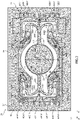
Figures 2-4 are top views of respective embodiments of the MEMS device ofFigure 1 ; -
Figure 5 is a block diagram schematically showing an electronic apparatus comprising the MEMS device ofFigure 1 ; and -
Figure 6 is an electrical circuit schematically showing a differential acquisition circuit of the electronic apparatus ofFigure 5 . - Elements common to the different embodiments of the present invention, described hereinafter, are indicated with the same reference numbers.
-
Figure 1 schematically shows, in a lateral crosssection view in a Cartesian (triaxial) reference system of axes X, Y, Z, aMEMS device 20, in particular a mirror device. - The
MEMS device 20 is formed in asemiconductor body 21. For example, thesemiconductor body 21 may be a die of semiconductor material, in particular mono- or polycrystalline silicon, or a double structural layer, for example formed by one SOI (Silicon On Insulator) wafer. - The
MEMS device 20 is provided with atiltable structure 22, having a main extension in a XY horizontal plane, defined by the X and Y axes, and arranged so as to rotate around a rotation axis A, parallel to the X axis. - The rotation axis A also represents a first median axis of symmetry for the
MEMS device 20, therefore also indicated with A; a second median axis of symmetry C for theMEMS device 20 is parallel to the Y axis and passing through a center O of thetiltable structure 22. - The
tiltable structure 22 is suspended above acavity 23 formed in thesemiconductor body 21 by afixed structure 24 of thesemiconductor body 21. Thetiltable structure 22 carries at the top a reflective surface 22' of theMEMS device 20, so as to define a mirror structure comprising thetiltable structure 22 and the reflective surface 22'. The reflective surface 22' is of a suitable material, for example aluminum, or gold, depending on whether the projection is in the visible or in the infrared. - The
tiltable structure 22 is elastically coupled to an anchor structure, here formed by a frame portion 24' of thefixed structure 24, through a support structure comprising a first and a second support arm, not shown inFigure 1 as extending longitudinally along the first median axis of symmetry A, above thecavity 23, between the frame portion 24' of thefixed structure 24 and thetiltable structure 22, from opposite parts thereof. The support arms are equal to each other and arranged symmetrically with respect to the second median axis of symmetry C. - The
MEMS device 20 also comprises a plurality ofactuation structures 30 which, as shown in greater detail inFigure 2 , extend between the frame portion 24' of thefixed structure 24 and the support structure, on sides of the latter which are opposite to each other along the Y axis and having therespective actuation structures 30 facing thereto. In particular, theactuation structures 30 have a symmetrical structure with respect to the first median axis of symmetry A. - The
actuation structures 30 are suspended above thecavity 23 and include, at top surfaces 30' thereof (not facing the cavity 23), respective piezoelectric actuator elements of theMEMS device 20, not shown inFigure 1 and electrically controllable to cause a mechanical deformation of the actuation structures which induces a torsion of the support arms around the first median axis of symmetry A and, therefore, a displacement of the mirror structure (in detail, a rotation of thetiltable structure 22 around the first median axis of symmetry A). In particular, eachactuation structure 30 comprises a respective actuation support body 31 (suspended above thecavity 23 and for example of semiconductor material) and the respective piezoelectric actuator element extending on theactuation support body 31; eachactuation support body 31 has said top surface 30' opposite to thecavity 23 and the piezoelectric actuator element extends on the top surface 30'. Therefore, each piezoelectric actuator element faces the respective top surface 30'. - Furthermore, the
MEMS device 20 comprises a plurality of displacement sensors (indicated inFigure 1 with the references 41A1 and 41A2, as better described below) of piezoelectric type which are galvanically isolated with respect to the piezoelectric actuator elements, are carried by theactuation structures 30 in a symmetrical manner with respect to the first median axis of symmetry A (in particular they extend on the top surfaces 30' of the actuation structures 30), and are suspended on thecavity 23. - In detail, each displacement sensor comprises a respective
piezoelectric layer 42a (in detail, of piezoelectric material, and in greater detail of insulating and piezoelectric material such as PZT or AlN) interposed, along the Z axis (i.e. orthogonally to the top surface 30' of therespective actuation structure 30 having the displacement sensor arranged thereon), between a respectivetop electrode 42b and arespective bottom electrode 42c, the latter being in contact with the top surface 30' of therespective actuation structure 30 having the displacement sensor arranged thereon. In other words, for each displacement sensor, thepiezoelectric layer 42a has a first and a second surface opposite to each other along the Z axis, where thetop electrode 42b is in contact with the first surface and thebottom electrode 42c is in contact with the second surface. Each displacement sensor thus forms a respective capacitor, where thetop electrode 42b and thebottom electrode 42c (for example both of metal material such as platinum) are frames or plates of the capacitor. In use, for each displacement sensor, the mechanical deformation of theactuation structures 30 caused by the piezoelectric actuator elements generates a corresponding mechanical deformation in the displacement sensors and therefore, due to the direct piezoelectric effect, there are generated an accumulation of charges of opposite sign at the first and the second surfaces of thepiezoelectric layer 42a (in particular, positive charges at the interface with the bottom/top electrode where the crystal lattice is subject to compression and negative charges at the interface with the top/bottom electrode where the crystal lattice is subject to expansion), and therefore a potential difference between thetop electrode 42b and thebottom electrode 42c. As a result, each displacement sensor generates a respective sensing signal (i.e. such potential difference) which is correlated to the rotation of thetiltable structure 22 around the rotation axis A and which is provided outside theMEMS device 20, as better discussed hereinafter with reference toFigure 5 . - In greater detail, the
MEMS device 20 comprises at least a first displacement sensor 41A1 and a second displacement sensor 41A2 arranged on theactuation structures 30, from parts opposite to each other with respect to the first median axis of symmetry A. Since the first and the second displacement sensors 41A1, 41A2 are arranged symmetrically with respect to the first median axis of symmetry A, they are subject to deformation movements along the Z axis which are opposite to each other: for example, if the first surface of thepiezoelectric layer 42a of the first displacement sensor 41A1 is subject to compression of the crystal lattice and the second surface of thepiezoelectric layer 42a of the first displacement sensor 41A1 is subject to expansion of the crystal lattice, then the first surface of thepiezoelectric layer 42a of the second displacement sensor 41A2 is subject to expansion of the crystal lattice and the second surface of thepiezoelectric layer 42a of the second displacement sensor 41A2 is subject to compression of the crystal lattice. As a result, the accumulation of charges on the first and second surfaces of thepiezoelectric layer 42a is opposite for the first and the second displacement sensors 41A1, 41A2, and the respective sensing signals generated thereby are in phase opposition (counterphase) to each other and may be acquired in a differential manner, as better described hereinafter with reference toFigure 6 . - As an alternative to what has been previously discussed, as shown for example in
Figure 3 , theactuation structures 30 may extend between the frame portion 24' of thefixed structure 24 and thetiltable structure 22, so as to face said sides of the support structure opposite to each other along the Y axis. In particular, theactuation structures 30 have a symmetrical structure with respect to the first median axis of symmetry A and to the second median axis of symmetry C. In this case, therefore, theactuation structures 30 are directly coupled to thetiltable structure 22, and are not instead directly coupled to the support structure. -
Figure 2 schematically shows theMEMS device 20, according to an embodiment similar to that shown inFigure 1 and wherein theMEMS device 20 is designed to operate in dynamic regime (i.e. in resonance, at rotation frequencies of thetiltable structure 22 which are higher than 10 kHz). - The
MEMS device 20 is formed in thesemiconductor body 21 and is provided with thetiltable structure 22. - The
tiltable structure 22 is suspended above thecavity 23 and carries at the top the reflective surface 22' which has, in the illustrated embodiment, a generally circular shape in the XY plane (although other shapes are possible, from an elliptical shape to a polygonal shape, for example square or rectangular). - The
tiltable structure 22 is elastically coupled to the frame portion 24' of thefixed structure 24 through the support structure comprising the first and the second support arms, indicated inFigure 2 with thereferences support arms cavity 23, between the frame portion 24' of thefixed structure 24 and thetiltable structure 22, from opposite parts thereof. Thesupport arms - In detail, the
first support arm 25A has afirst end 25A' rigidly coupled to thetiltable structure 22 and asecond end 25A" rigidly coupled to the frame portion 24' of thefixed structure 24 and comprises a first and a secondtorsional spring torsional springs tiltable structure 22 and a first side of the frame portion 24' of thefixed structure 24. - The
second support arm 25B has afirst end 25B' rigidly coupled to thetiltable structure 22 and asecond end 25B" rigidly coupled to the frame portion 24' of thefixed structure 24 and comprises a third and a fourthtorsional spring torsional springs tiltable structure 22 and a second side, opposite to the first, of the frame portion 24' of thefixed structure 24. - In detail, the
torsional springs - In the
first support arm 25A, the first and the second torsional springs 27A, 28A are connected to each other at afirst constraint structure 29A, which is rigid; in thesecond support arm 25B, the third and the fourth torsional springs 27B, 28B are connected to each other at asecond constraint structure 29B, which is rigid. - The
MEMS device 20 further comprises the plurality ofactuation structures 30 of resonant type, and in particular at least one first and a second actuation structure 30A1 and 30A2, extending between the frame portion 24' of the fixedstructure 24 and thefirst constraint structure 29A, on a first and, respectively, a second side of thefirst support arm 25A, and have a symmetrical structure with respect to the first median axis of symmetry A. In detail, the first actuation structure 30A1 is coupled to thefirst constraint structure 29A through a coupling region 35A1 of the first actuation structure 30A1, which extends along a direction of main extension transverse with respect to a direction of main extension of the remaining portion of the first actuation structure 30A1; similarly, the second actuation structure 30A2 is coupled to thefirst constraint structure 29A through a coupling region 35A2 of the second actuation structure 30A2, which extends along a respective direction of main extension transverse with respect to a direction of main extension of the remaining portion of the second actuation structure 30A2. - The plurality of
actuation structures 30 further comprises a third and a fourth actuation structure 30B1 and 30B2, extending between the frame portion 24' of the fixedstructure 24 and thesecond constraint structure 29B, on a first and, respectively, a second side of thesecond support arm 25B. The third and the fourth actuation structures 30B1 and 30B2 have a structure symmetrical to each other with respect to the first median axis of symmetry A. In detail, the third actuation structure 30B1 is coupled to thesecond constraint structure 29B through a coupling region 35B1 of the third actuation structure 30B1, which extends along a respective direction of main extension transverse with respect to a direction of main extension of the remaining portion of the third actuation structure 30B1; similarly, the fourth actuation structure 30B2 is coupled to thesecond constraint structure 29B through a coupling region 35B2 of the fourth actuation structure 30B2 which extends along a respective direction of main extension transverse with respect to a direction of main extension of the remaining portion of the fourth actuation structure 30B2. - The actuation structures 30A1, 30A2, 30B1 and 30B2 are suspended above the
cavity 23 and include, at the top surfaces 30' thereof, the respective piezoelectric actuator elements, indicated inFigure 2 with the references 38A1, 38A2, 38B1, 38B2. In particular, the piezoelectric actuator elements 38A1, 38A2, 38B1, 38B2 are based on the reverse piezoelectric effect and have a structure similar to the displacement sensors (therefore each of them comprises, in a manner not shown inFigure 2 , the respectivepiezoelectric layer 42a, the respectivetop electrode 42b and therespective bottom electrode 42c), and therefore are not further described herein. - Furthermore, the
MEMS device 20 comprises the plurality of displacement sensors, and in particular comprises the first and the second displacement sensors 41A1 and 41A2. The first and the second displacement sensors 41A1 and 41A2 extend for example on the first and, respectively, on the second actuation structures 30A1, 30A2 (alternatively and in a manner not shown, they extend on the third and, respectively, on the fourth actuation structures 30B1, 30B2), in particular on the top surfaces 30' thereof. For example, the first and the second displacement sensors 41A1 and 41A2 extend at the frame portion 24' of the fixedstructure 24. - Optionally, the plurality of displacement sensors also comprises a third and a fourth displacement sensor 41B1 and 41B2 extending on the third and, respectively, on the fourth actuation structures 30B1, 30B2, in particular on the top surfaces 30' thereof. For example, the third and the fourth displacement sensors 41B1 and 41B2 extend at the frame portion 24' of the fixed
structure 24. - Furthermore, optionally the
MEMS device 20 comprises a plurality ofelectrical contact pads 40, carried by the frame portion 24' of the fixedstructure 24 and electrically connected to the piezoelectric actuator elements 38A1, 38A2, 38B1, 38B2, to allow the electrical bias through actuation signals coming from the outside of the MEMS device 20 (better discussed hereinafter with reference toFigure 5 ), and electrically connected to the first and the second displacement sensors 41A1 and 41A2 (optionally, also to the third and the fourth displacement sensors 41B1 and 41B2, if any), to allow the respective potential differences to be sensed. In particular, the pads 40 comprise: a first pad of first actuator 40A1' electrically connected, through a first conductive via of first actuator 43A1', to the top electrodes 42b of the piezoelectric actuator elements 38A1 and 38B1; a second pad of first actuator 40A1" electrically connected, through a second conductive via of first actuator 43A1", to the bottom electrodes 42c of the piezoelectric actuator elements 38A1 and 38B1; a first pad of first sensor 40C1' electrically connected, through a first conductive via of first sensor 43C1', to the top electrode 42b of the first displacement sensor 41A1; a second pad of first sensor 40C1" electrically connected, through a second conductive via of first sensor 43C1", to the bottom electrode 42c of the first displacement sensor 41A1; a first pad of second actuator 40A2' electrically connected, through a first conductive via of second actuator 43A2', to the top electrodes 42b of the piezoelectric actuator elements 38A2 and 38B2; a second pad of second actuator 40A2" electrically connected, through a second conductive via of second actuator 43A2", to the bottom electrodes 42c of the piezoelectric actuator elements 38A2 and 38B2; a first pad of second sensor 40C2' electrically connected, through a first conductive via of second sensor 43C2', to the top electrode 42b of the second displacement sensor 41A2; and a second pad of second sensor 40C2" electrically connected, through a second conductive via of second sensor 43C2", to the bottom electrode 42c of the second displacement sensor 41A2. - Optionally, the
MEMS device 20 further comprises a first and a secondintegrated capacitor semiconductor body 21, for example in the fixedstructure 24. In a manner not shown inFigure 2 , eachintegrated capacitor pads 40 further comprise: a first pad of first capacitor 40D1' electrically connected to the top plate of the firstintegrated capacitor 65A; a second pad of first capacitor 40D1" electrically connected, through a conducive via of first capacitor 43D1", to the bottom plate of the firstintegrated capacitor 65A; a first pad of second capacitor 40D2' electrically connected to the top plate of the secondintegrated capacitor 65B; a second pad of second capacitor 40D2" electrically connected, through a conductive via of second capacitor 43D2", to the bottom plate of the secondintegrated capacitor 65B. The use of theintegrated capacitors Figure 6 . -
Figure 3 schematically shows theMEMS device 20, according to a further embodiment wherein theMEMS device 20 is designed to operate in quasi-static (i.e., at rotation frequencies of thetiltable structure 22 which are lower than approximately 200 Hz). In particular, the structure of the MEMS device ofFigure 3 is similar to that ofFigure 2 , and therefore it is not described again in detail herein. - However, in
Figure 3 , theactuation structures 30 extend between the frame portion 24' of the fixedstructure 24 and thetiltable structure 22, on sides of the latter which are opposite to each other along the X axis. Therefore, theactuation structures 30 are directly coupled to thetiltable structure 22, and are not instead directly coupled to the support structure as described with reference toFigure 2 . -
Figure 4 schematically shows theMEMS device 20, according to a further embodiment. In particular, the structure of the MEMS device ofFigure 4 is similar to that ofFigure 2 , and therefore it is not described again in detail herein. - However, in
Figure 4 , the third and the fourth displacement sensors 41B1 and 41B2, which are electrically arranged in series with the first and, respectively, the second displacement sensors 41A1 and 41A2 are also present. In other words, the capacitors formed by the first and the third displacement sensors 41A1 and 41B1 are in series with each other, and the capacitors formed by the second and the fourth displacement sensors 41A2 and 41B2 are in series with each other. In particular, thebottom electrode 42c of the first displacement sensor 41A1 is electrically connected, through a first common conductive via ofsensor 43E', to thetop electrode 42b of the third displacement sensor 41B1 and, similarly, thebottom electrode 42c of the second displacement sensor 41A2 is electrically connected, through a second common conductive via ofsensor 43E", to thetop electrode 42b of the fourth displacement sensor 41B2. - Furthermore, in
Figure 4 , the second pad of first sensor 40C1", the second conductive via of first sensor 43C1", the second pad of second sensor 40C2", the second conductive via of second sensor 43C2" are absent. In lieu thereof, thepads 40 comprise: a first pad of third sensor 40C3' electrically connected, through a first conductive via of third sensor 43C3', to thebottom electrode 42c of the third displacement sensor 41B1; and a first pad of fourth sensor 40C4' electrically connected, through a first conductive via of fourth sensor 43C4', to thebottom electrode 42c of the fourth displacement sensor 41B2. -
Figure 5 shows an electronic apparatus 50 (e.g., a laser projector for "Virtual Retinal Display", VRD) comprising theMEMS device 20 according to any of the previously described embodiments, and a control unit 52 (e.g., an electronic processing circuit such as an ASIC - Application Specific Integrated Circuit) coupled to theMEMS device 20. - In particular, the
control unit 52 comprises adifferential acquisition module 54 electrically coupled to the displacement sensors 41A1, 41A2, 41B1, 41B2 to receive the respective sensing signals therefrom and to process the latter in a differential manner. In detail, the sensing signals are acquired, in a differential manner, by thedifferential acquisition module 54 which, on the basis of the sensing signals, generates a respective displacement signal indicative of the sensed displacement of thetiltable structure 22 at output. - Optionally, the
control unit 52 further comprises abiasing module 56 electrically coupled to the piezoelectric actuator elements 38A1, 38A2, 38B1, 38B2 to send the respective actuation signals thereto and thus control the rotation of thetiltable structure 22. - For example, the actuation signals are generated, according to known closed-loop control techniques, as a function of the displacement signal generated by the
differential acquisition module 54. - Additionally, or alternatively, the displacement signal may be used to verify the correct operation of the MEMS device 20 (i.e. the correct position of the
tiltable structure 22 with respect to a target position). This allows the light beam deflected by thetiltable structure 22 to be controlled, thus ensuring the correct angular scanning performed by theMEMS device 20; furthermore, in VRD applications, this prevents the light beam incident on thetiltable structure 22 from being generated when thetiltable structure 22 is not moving, which might cause light emission beyond the safety thresholds for the human eye. -
Figure 6 shows adifferential acquisition circuit 58 comprised in thedifferential acquisition module 54 and electrically coupled to theMEMS device 20. - In particular, the
MEMS device 20 is represented by an equivalent electrical circuit which comprises: a first series circuit of afirst voltage generator 62A and afirst capacitor 64A, which extend between afirst node 60A and asecond node 60B; and a second series circuit of asecond voltage generator 62B and asecond capacitor 64B, which extend between athird node 60C and afourth node 60D. Considering the cases ofFigures 2 and3 , thenodes Figure 4 , thenodes - In the embodiments of
Figures 2 and3 wherein the sensing signals are generated by the first and the second displacement sensors 41A1, 41A2 only, thefirst voltage generator 62A generates a voltage Vsense1 which is equal to the potential difference (indicated hereinafter with VA1) generated by the first displacement sensor 41A1, thesecond voltage generator 62B generates a voltage Vsense2 which is equal to the potential difference (indicated hereinafter with VA2) generated by the second displacement sensor 41A2, thefirst capacitor 64A has a capacitance CPS1 equal to a capacitance CA1 of the first displacement sensor 41A1, and thesecond capacitor 64B has a capacitance CPS2 equal to a capacitance CA2 of the second displacement sensor 41A2. - In the embodiment of
Figure 4 wherein the sensing signals are generated by the displacement sensors 41A1, 41A2, 41B1 and 41B2, thefirst voltage generator 62A generates the voltage Vsense1 which is equal to the sum of the potential difference VA1 generated by the first displacement sensor 41A1 and of the potential difference (indicated hereinafter with VB1) generated by the third displacement sensor 41B1, thesecond voltage generator 62B generates the voltage Vsense2 which is equal to the sum of the potential difference VA2 generated by the second displacement sensor 41A2 and of the potential difference (indicated hereinafter with VB2) generated by the fourth displacement sensor 41B2, thefirst capacitor 64A has the capacitance CPS1 equal to the series (i.e. to the reciprocal of the sum of the reciprocals) of the capacitance CA1 of the first displacement sensor 41A1 and of a capacitance CB1 of the third displacement sensor 41B1, and thesecond capacitor 64B has the capacitance CPS2 equal to the series of the capacitance CA2 of the second displacement sensor 41A2 and of a capacitance CB2 of the fourth displacement sensor 41B2. - Furthermore, in
Figure 6 , the second and thefourth nodes intermediate node 60E is present therebetween. Optionally, a common mode voltage VCM is applied to theintermediate node 60E and is indicative of a direct common mode voltage supplied to the displacement sensors 41A1 and 41A2 (considering, by way of example, the cases ofFigures 2 and3 ) through the second pad of first sensor 40C1" and, respectively, the second pad of second sensor 40C2", for the reasons described hereinafter. Considering instead the case ofFigure 4 , the common mode voltage VCM is indicative of a direct common mode voltage supplied to the displacement sensors 41A1, 41A2 41B1, 41B2 through the first pad of third sensor 40C3' and the first pad of fourth sensor 40C4'. For example, this direct common mode voltage is supplied by the control unit 52 (e.g., by the biasing module 56). - The
differential acquisition circuit 58 comprises an operational amplifier of differential type, in particular a fully-differential amplifier (FDA) 58' such as a fully-differential charge amplifier. In detail, the FDA 58' has differential inputs and outputs, and in particular it has apositive input 66a, anegative input 66b, a negative output 66c and apositive output 66d. Thepositive input 66a is coupled to thefirst node 60A and, furthermore, it is coupled to the negative output 66c through a first parallel circuit of afirst feedback resistor 68A and of afirst feedback capacitor 67A. Thenegative input 66b is coupled to thethird node 60C and, furthermore, is coupled to thepositive output 66d through a second parallel circuit of asecond feedback resistor 68B and of asecond feedback capacitor 67B. In particular, thefeedback resistors second feedback capacitors second feedback resistors second capacitors Figure 4 ). In this case, a gain of the FDA 58' is proportional to the CPSX/CFB ratio, where CPSX=CPS1=CPS1 and CFB=CFB1=CFB2. - According to an aspect of the present invention, the first and the
second feedback capacitors integrated capacitors MEMS device 20. - In use, due to the displacement of the
tiltable structure 22, the MEMS device generates the sensing signals. Due to these sensing signals, a differential voltage Vdiff (or differential signal), which is correlated to the displacement signal, is generated between the negative output 66c and thepositive output 66d. - In fact, the displacement signal is obtained, through known signal processing techniques, from the differential voltage Vdiff. For example, in a manner not shown, the
differential acquisition module 54 further comprises an analog-to-digital converter (ADC) and, optionally, a filtering module to convert the differential voltage Vdiff into digital and to filter this signal in the frequency domain, thus obtaining the displacement signal. Furthermore, in a manner not shown, a direct bias voltage is supplied to the FDA 58', in order to bias the latter in a per se known manner. Furthermore, since the displacement sensors 41A1, 41A2 (and 41B1, 41B2 if in the case ofFigure 4 ) generally have respective leakage resistors (not shown and, by way of example, arranged in parallel to the first and, respectively, thesecond capacitors positive input 66a and thenegative input 66b of the FDA 58'). In fact, in absence of the common mode voltage VCM, if the leakage resistors have respective resistances that are comparable to the first and a second feedback resistance RFB1 and RFB2 (e.g., they have the same order of magnitude as the feedback resistances RFB1 and RFB2), the input common mode voltage of the FDA 58' might be subject to variations such that they compromise the optimal operation of the FDA 58'. On the other hand, when the common mode voltage VCM is present and the resistances of the leakage resistors are comparable to the first and the second feedback resistances RFB1 and RFB2, the input common mode voltage of the FDA 58' also depends on the common mode voltage VCM which may be applied to control the input common mode voltage of the FDA 58'. - From an examination of the characteristics of the invention made according to the present invention, the advantages that it allows to obtain are apparent.
- In particular, the displacement sensors 41A1, 41A2, 41B1, 41B2 of piezoelectric type and with acquisition of differential type allow the displacements of the
tiltable structure 22 to be accurately sensed, due also to their placing from parts opposite with respect to the first median axis of symmetry A which causes the sensing signals to be generated in phase opposition to each other. It is therefore possible to control the movements of thetiltable structure 22 more accurately than by means of known solutions. - The displacement sensors 41A1, 41A2, 41B1, 41B2, being of piezoelectric type, need a lower power consumption than that required by piezoresistive sensors.
- Furthermore, the process of manufacturing the
MEMS device 20 is simplified, since the manufacturing of the displacement sensors 41A1, 41A2, 41B1, 41B2 may take place simultaneously (i.e., exploiting the same manufacturing steps and adapting the masks already used) with respect to the manufacturing of the piezoelectric actuator elements 38A1, 38A2, 38B1, 38B2. In other words, no additional manufacturing steps are needed, and this reduces the overall cost of theMEMS device 20. - Furthermore, the
MEMS sensor 20 and thedifferential acquisition module 54 allow the movements of thetiltable structure 22 to be sensed with greater sensitivity with respect to the prior arts, achieving measure sensitivities which are even higher than approximately 12 mV/deg. Furthermore, the use of theMEMS sensor 20 and of thedifferential acquisition module 54 allows to obtain a measure of the displacement of thetiltable structure 22 which is not affected by temperature variations. - The use of the first and the third displacement sensors 41A1, 41B1, and of the second and the fourth displacement sensors 41A2, 41B2 in series, as described in
Figure 4 , allows the overall accumulation of charge to be increased due to a greater overall area of capacitor, while keeping the overall value of capacitance reduced (CPS1 is equal to the series of CA1 and CB1, and CPS2 is equal to the series of CA2 and CB2). - Furthermore, the presence of the first and the second
integrated capacitors semiconductor body 21, allows to have a better control of the manufacturing tolerances of thefeedback capacitors feedback capacitors feedback capacitors semiconductor body 21 has the further advantage of exploiting, effectively and without requiring additional costs, an area of thesemiconductor body 21 that otherwise would still be present but unused. - Finally, it is apparent that modifications and variations may be made to the invention described and illustrated herein without thereby departing from the scope of the present invention, as defined in the attached claims.
- For example, considering the embodiments of
Figures 2 and3 , the displacement sensors 41A1, 41A2 may not be galvanically isolated with respect to the respective piezoelectric actuator elements 38A1, 38A2. In fact, thebottom electrodes 42c of the first displacement sensor 41A1 and of the first piezoelectric actuator element 38A1 may be in electrical contact with each other, as well as thebottom electrodes 42c of the second displacement sensor 41A2 and of the second piezoelectric actuator element 38A2. Similar considerations may be made by considering, instead of thebottom electrodes 42c, thetop electrodes 42b. - Furthermore, the use of the displacement sensors 41A1, 41A2, 41B1, 41B2 as shown in
Figure 4 is not limited to the structure of theMEMS device 20 shown inFigure 4 , but may be similarly applied to the structure of theMEMS device 20 shown inFigure 3 .
Claims (16)
- A MEMS device (20) comprising:- a semiconductor body (21) defining a cavity (23) and forming an anchor portion (24');- a tiltable structure (22) elastically suspended on the cavity (23);- a first and a second support arm (25A, 25B) extending between the anchor portion (24') and opposite sides of the tiltable structure (22), along a rotation axis (A) of the tiltable structure (22);- a first and a second piezoelectric actuation structure (30A1, 30A2) which face opposite sides of the first support arm (25A), extend between the anchor portion (24') and said opposite sides of the first support arm (25A) or between the anchor portion (24') and the tiltable structure (22), and are biasable to deform mechanically thereby generating a rotation of the tiltable structure (22) around the rotation axis (A);- a first (41A1) and a second displacement sensor (41A2) of piezoelectric type, which are carried by the first and, respectively, the second piezoelectric actuation structures (30A1, 30A2) and are opposite to each other with respect to the rotation axis (A),wherein, when the tiltable structure (22) rotates around the rotation axis (A) due to the first and the second piezoelectric actuation structures (30A1, 30A2), the first and the second displacement sensors (41A1, 41A2) are subject to respective mechanical deformations and generate a first and, respectively, a second sensing signal which are in phase opposition to each other and are indicative of the rotation of the tiltable structure (22) around the rotation axis (A), andwherein the first and the second sensing signals are configured to be acquired in a differential manner.
- The MEMS device according to claim 1, wherein the first and the second displacement sensors (41A1, 41A2) are electrically couplable to a differential acquisition module (54) configured to acquire, in a differential manner, the first and the second sensing signals and to generate, on the basis of the first and the second sensing signals, a differential signal indicative of the rotation of the tiltable structure (22) around the rotation axis (A).
- The MEMS device according to claim 2, wherein the differential acquisition module (54) comprises a differential acquisition circuit (58) formed by:- a fully-differential amplifier (58') having a positive input (66a), a negative input (66b), a negative output (66c) and a positive output (66d), the positive input (66a) being electrically coupled to the first displacement sensor (41A1) and the negative input (66b) being electrically coupled to the second displacement sensor (41A2);- a first parallel circuit comprising a first feedback resistor (68A) and a first feedback capacitor (67A), the first parallel circuit extending between the positive input (66a) and the negative output (66c); and- a second parallel circuit comprising a second feedback resistor (68B) and a second feedback capacitor (67B), the second parallel circuit extending between the negative input (66b) and the positive output (66d),
wherein, when the tiltable structure (22) rotates around the rotation axis (A) due to the first and the second piezoelectric actuation structures (30A1, 30A2), a differential voltage (Vdiff) is generated between the negative output (66c) and the positive output (66d), the differential voltage (Vdiff) being said differential signal. - The MEMS device according to claim 3, wherein the first and the second feedback capacitors (67A, 67B) are integrated in the semiconductor body (21).
- The MEMS device according to any of the preceding claims, wherein the first and the second displacement sensors (41A1, 41A2) extend on respective top surfaces (30') of the first and, respectively, the second piezoelectric actuation structures (30A1, 30A2),
wherein each of the first and the second displacement sensors (41A1, 41A2) comprises a respective top electrode (42b), a respective bottom electrode (42c) and a respective piezoelectric layer (42a) interposed, orthogonally to the respective top surface (30'), between the respective top electrode (42b) and the respective bottom electrode (42c) which is in contact with the respective top surface (30') of the first or, respectively, the second piezoelectric actuation structures (30A1, 30A2). - The MEMS device according to any of the preceding claims, further comprising:- a third and a fourth piezoelectric actuation structure (30B1, 30B2) which face opposite sides of the second support arm (25B), extend between the anchor portion (24') and said opposite sides of the second support arm (25B) or between the anchor portion (24') and the tiltable structure (22), and are biasable to deform mechanically thereby generating the rotation of the tiltable structure (22) around the rotation axis (A); and- a third (41B1) and a fourth (41B2) displacement sensor of piezoelectric type, which are carried by the third and, respectively, the fourth piezoelectric actuation structures (30B1, 30B2) and are opposite to each other with respect to the rotation axis (A),
wherein, when the tiltable structure (22) rotates around the rotation axis (A) due to the first, the second, the third and the fourth piezoelectric actuation structures (30A1, 30A2, 30B1, 30B2), the first, the second, the third and the fourth displacement sensors (41A1, 41A2, 41B1, 41B2) are subject to respective mechanical deformations and generate, respectively, the first, the second, a third and a fourth sensing signals, the third and the fourth sensing signals being in phase opposition to each other and being indicative of the rotation of the tiltable structure (22) around the rotation axis (A). - The MEMS device according to claim 6, wherein the first and the third displacement sensors (41A1, 41B1) are electrically connected in series with each other, and wherein the second and the fourth displacement sensors (41A2, 41B2) are electrically connected in series with each other.
- The MEMS device according to claim 5 and claim 7, wherein the third and the fourth displacement sensors (41B1, 41B2) extend on respective top surfaces (30') of the third and, respectively, the fourth piezoelectric actuation structures (30B1, 30B2),wherein each of the third and the fourth displacement sensors (41B1, 41B2) comprises a respective top electrode (42b), a respective bottom electrode (42c) and a respective piezoelectric layer (42a) interposed, orthogonally to the respective top surface (30'), between the respective top electrode (42b) and the respective bottom electrode (42c) which is in contact with the respective top surface (30') of the third or, respectively, the fourth piezoelectric actuation structures (30B1, 30B2),wherein the bottom electrode (42c) of the first displacement sensor (41A1) is electrically coupled to the top electrode (42b) of the third displacement sensor (41B1), and wherein the bottom electrode (42c) of the second displacement sensor (41A2) is electrically coupled to the top electrode (42b) of the fourth displacement sensor (41B2).
- The MEMS device according to claim 2 and one of claims 7 and 8, wherein the first, the second, the third and the fourth displacement sensors (41A1, 41A2, 41B1, 41B2) are electrically coupled to the differential acquisition module (54) which is configured to acquire, in a differential manner, the sum of the first and the third sensing signals and the sum of the second and the fourth sensing signals and to generate, on the basis of the sum of the first and the third sensing signals and on the basis of the sum of the second and the fourth sensing signals, said differential signal.
- The MEMS device according to any of the preceding claims, wherein the first and the second piezoelectric actuation structures (30A1, 30A2) comprise a first (38A1) and, respectively, a second piezoelectric actuator element (38A2) of piezoelectric type, which are opposite to each other with respect to the rotation axis (A),
wherein the first displacement sensor (41A1) and the first piezoelectric actuator element (38A1) are galvanically isolated from each other, and wherein the second displacement sensor (41A2) and the second piezoelectric actuator element (38A2) are galvanically isolated from each other. - The MEMS device according to claim 5, wherein the first and the second piezoelectric actuation structures (30A1, 30A2) comprise a first (38A1) and, respectively, a second piezoelectric actuator element (38A2) of piezoelectric type, which are opposite to each other with respect to the rotation axis (A),wherein the first and the second piezoelectric actuator elements (38A1, 38A2) face the respective top surfaces (30') of the first and, respectively, the second piezoelectric actuation structures (30A1, 30A2),wherein each of the first and the second piezoelectric actuator elements (38A1, 38A2) comprises a respective top electrode (42b), a respective bottom electrode (42c) and a respective piezoelectric layer (42a) interposed, orthogonally to the respective top surface (30'), between the respective top electrode (42b) and the respective bottom electrode (42c),wherein the bottom electrodes (42c) or the top electrodes (42b) of the first displacement sensor (41A1) and the first piezoelectric actuator element (38A1) are electrically coupled to each other, and wherein the bottom electrodes (42c) or the top electrodes (42b) of the second displacement sensor (41A2) and of the second piezoelectric actuator element (38A2) are electrically coupled to each other.
- The MEMS device according to any of the preceding claims, wherein the first and the second piezoelectric actuation structures (30A1, 30A2) are of resonant type,wherein the tiltable structure (22) has a main extension in a horizontal plane (XY) defined by a first and a second horizontal axis (X, Y) perpendicular to each other, the first horizontal axis (X) being parallel to the rotation axis (A),wherein the first support arm (25A) comprises a first and a second torsional spring (27A, 28A) rigid for movements outside the horizontal plane (XY) and yielding to torsion around the rotation axis (A), the first torsional spring (27A) being coupled to the tiltable structure, the second torsional spring (28A) being coupled to the anchor portion (24'), the first and the second torsional springs (27A, 28A) being mutually coupled at a first constraint region (29A), andwherein the first and the second piezoelectric actuation structures (38A1, 38A2) extend between the anchor portion (24') and the first constraint structure (29A), on the respective opposite sides of the first support arm (25A).
- The MEMS device according to any of the preceding claims, wherein the first and the second displacement sensors (41A1, 41A2) are configured to be biased with a direct common mode voltage (VCM).
- An electronic apparatus (50) comprising a MEMS device (20), according to any of claims 1-13, and a differential acquisition module (54) which is electrically coupled to the first and the second displacement sensors (41A1, 41A2) and is configured to acquire, in a differential manner, the first and the second sensing signals and to generate, on the basis of the first and the second sensing signals, a differential signal indicative of the rotation of the tiltable structure (22) around the rotation axis (A).
- The electronic apparatus (50) according to claim 14, further comprising a biasing module (56) coupled to the differential acquisition module (54) and to the first and the second piezoelectric actuation structures (30A1, 30A2), and configured to:- receive, from the differential acquisition module (54), a displacement signal correlated to the differential signal;- generate, on the basis of the displacement signal, actuation signals; and- bias, through the actuation signals, the first and the second piezoelectric actuation structures (30A1, 30A2).
- A method of using a MEMS device (20) according to any of claims 1-13, comprising the steps of:- biasing the first and the second piezoelectric actuation structures (30A1, 30A2) to generate the rotation of the tiltable structure (22) around the rotation axis (A); and- acquiring, in a differential manner, the first and the second sensing signals generated by the first and, respectively, the second displacement sensors (41A1, 41A2).
Applications Claiming Priority (1)
| Application Number | Priority Date | Filing Date | Title |
|---|---|---|---|
| IT102021000009635A IT202100009635A1 (en) | 2021-04-16 | 2021-04-16 | MEMS DEVICE WITH TURNTABLE STRUCTURE AND IMPROVED CONTROL |
Publications (2)
| Publication Number | Publication Date |
|---|---|
| EP4075184A1 true EP4075184A1 (en) | 2022-10-19 |
| EP4075184B1 EP4075184B1 (en) | 2025-03-19 |
Family
ID=76708332
Family Applications (1)
| Application Number | Title | Priority Date | Filing Date |
|---|---|---|---|
| EP22167952.5A Active EP4075184B1 (en) | 2021-04-16 | 2022-04-12 | Electronic apparatus comprising a mems device with tiltable structure and improved control |
Country Status (4)
| Country | Link |
|---|---|
| US (1) | US12066621B2 (en) |
| EP (1) | EP4075184B1 (en) |
| CN (2) | CN115215282A (en) |
| IT (1) | IT202100009635A1 (en) |
Cited By (1)
| Publication number | Priority date | Publication date | Assignee | Title |
|---|---|---|---|---|
| IT202300003498A1 (en) | 2023-02-27 | 2024-08-27 | St Microelectronics Int Nv | MEMS DEVICE, ESPECIALLY OF THE MIRROR TYPE, WITH IMPROVED DETECTION OF THE DEFORMABLE STRUCTURE OF THE SAME, AND MANUFACTURING PROCESS OF THE MEMS DEVICE |
Families Citing this family (1)
| Publication number | Priority date | Publication date | Assignee | Title |
|---|---|---|---|---|
| IT202100009635A1 (en) * | 2021-04-16 | 2022-10-16 | St Microelectronics Srl | MEMS DEVICE WITH TURNTABLE STRUCTURE AND IMPROVED CONTROL |
Citations (2)
| Publication number | Priority date | Publication date | Assignee | Title |
|---|---|---|---|---|
| CN108761773A (en) | 2018-06-15 | 2018-11-06 | 重庆大学 | A kind of MOEMS raster micro mirrors of the non-homogeneous folded beam driving of piezoelectricity |
| EP3715317A1 (en) | 2019-03-29 | 2020-09-30 | STMicroelectronics S.r.l. | Resonant mems device having a tiltable, piezoelectrically controlled structure, in particular a micromirror |
Family Cites Families (6)
| Publication number | Priority date | Publication date | Assignee | Title |
|---|---|---|---|---|
| JP5493735B2 (en) * | 2009-01-30 | 2014-05-14 | 株式会社リコー | Deflection mirror, optical scanning device, image forming device, and image projection device |
| CN101852917B (en) * | 2010-03-31 | 2012-02-22 | 重庆大学 | Large turn angle piezoelectric scanning micromirror |
| CN107247330A (en) * | 2017-08-11 | 2017-10-13 | 重庆大学 | The integrated MOEMS raster micro mirror of piezoelectric type |
| EP3666727B1 (en) * | 2018-12-14 | 2024-10-02 | STMicroelectronics S.r.l. | Microelectromechanical device with a structure tiltable by piezoelectric actuation having improved mechanical and electrical characteristics |
| US11835710B2 (en) * | 2020-12-15 | 2023-12-05 | Infineon Technologies Ag | Method of mode coupling detection and damping and usage for electrostatic MEMS mirrors |
| IT202100009635A1 (en) * | 2021-04-16 | 2022-10-16 | St Microelectronics Srl | MEMS DEVICE WITH TURNTABLE STRUCTURE AND IMPROVED CONTROL |
-
2021
- 2021-04-16 IT IT102021000009635A patent/IT202100009635A1/en unknown
-
2022
- 2022-04-12 EP EP22167952.5A patent/EP4075184B1/en active Active
- 2022-04-14 US US17/720,506 patent/US12066621B2/en active Active
- 2022-04-15 CN CN202210397660.2A patent/CN115215282A/en active Pending
- 2022-04-15 CN CN202220875855.9U patent/CN218145865U/en active Active
Patent Citations (2)
| Publication number | Priority date | Publication date | Assignee | Title |
|---|---|---|---|---|
| CN108761773A (en) | 2018-06-15 | 2018-11-06 | 重庆大学 | A kind of MOEMS raster micro mirrors of the non-homogeneous folded beam driving of piezoelectricity |
| EP3715317A1 (en) | 2019-03-29 | 2020-09-30 | STMicroelectronics S.r.l. | Resonant mems device having a tiltable, piezoelectrically controlled structure, in particular a micromirror |
Cited By (2)
| Publication number | Priority date | Publication date | Assignee | Title |
|---|---|---|---|---|
| IT202300003498A1 (en) | 2023-02-27 | 2024-08-27 | St Microelectronics Int Nv | MEMS DEVICE, ESPECIALLY OF THE MIRROR TYPE, WITH IMPROVED DETECTION OF THE DEFORMABLE STRUCTURE OF THE SAME, AND MANUFACTURING PROCESS OF THE MEMS DEVICE |
| EP4421551A1 (en) | 2023-02-27 | 2024-08-28 | STMicroelectronics International N.V. | Mems device, in particular of mirror type, with improved detection of the deformation of a deformable structure of the same, and manufacturing process of the mems device |
Also Published As
| Publication number | Publication date |
|---|---|
| CN115215282A (en) | 2022-10-21 |
| US20220334378A1 (en) | 2022-10-20 |
| IT202100009635A1 (en) | 2022-10-16 |
| US12066621B2 (en) | 2024-08-20 |
| EP4075184B1 (en) | 2025-03-19 |
| CN218145865U (en) | 2022-12-27 |
Similar Documents
| Publication | Publication Date | Title |
|---|---|---|
| US11933968B2 (en) | Biaxial resonant microelectromechanical mirror structure with piezoelectric actuation having improved characteristics | |
| US11656539B2 (en) | Microelectromechanical device with a structure tiltable by piezoelectric actuation having improved mechanical and electrical characteristics | |
| US6275326B1 (en) | Control arrangement for microelectromechanical devices and systems | |
| US7075700B2 (en) | Mirror actuator position sensor systems and methods | |
| US6411214B1 (en) | Method for sensing electrical current | |
| US6466005B2 (en) | High resolution current sensing apparatus | |
| EP4075184B1 (en) | Electronic apparatus comprising a mems device with tiltable structure and improved control | |
| TW201142242A (en) | Exposure method | |
| CN112573475B (en) | Waterproof button device, input device including button device, and electronic apparatus | |
| US12510749B2 (en) | Biaxial microelectromechanical mirror device with piezoelectric actuation | |
| EP4421551B1 (en) | Mems device, in particular of mirror type, with improved detection of the deformation of a deformable structure of the same, and manufacturing process of the mems device | |
| US20230228798A1 (en) | Method and device for measuring actuators in a projection exposure apparatus for semiconductor lithography | |
| CN218181210U (en) | Micro-electromechanical mirror device and optoelectronic system | |
| JP2773460B2 (en) | Semiconductor acceleration sensor | |
| EP4092475A1 (en) | Microelectromechanical mirror device with piezoelectric actuation and piezoresistive sensing having self-calibration properties | |
| EP4082962A1 (en) | Microelectromechanical mirror device with piezoelectric actuation and improved opening angle | |
| JP7681855B2 (en) | Acceleration Sensor Device | |
| JP2026516110A (en) | Adaptive Optics Module | |
| CN118545673A (en) | MEMS device and manufacturing process thereof | |
| CN121679894A (en) | Piezoelectric driving image motion compensation mirror device and control method | |
| CN116577939A (en) | An optical image stabilization device driven by a self-sensing piezoelectric actuator | |
| JPH10160752A (en) | Acceleration detector |
Legal Events
| Date | Code | Title | Description |
|---|---|---|---|
| PUAI | Public reference made under article 153(3) epc to a published international application that has entered the european phase |
Free format text: ORIGINAL CODE: 0009012 |
|
| STAA | Information on the status of an ep patent application or granted ep patent |
Free format text: STATUS: THE APPLICATION HAS BEEN PUBLISHED |
|
| AK | Designated contracting states |
Kind code of ref document: A1 Designated state(s): AL AT BE BG CH CY CZ DE DK EE ES FI FR GB GR HR HU IE IS IT LI LT LU LV MC MK MT NL NO PL PT RO RS SE SI SK SM TR |
|
| STAA | Information on the status of an ep patent application or granted ep patent |
Free format text: STATUS: REQUEST FOR EXAMINATION WAS MADE |
|
| 17P | Request for examination filed |
Effective date: 20230407 |
|
| RBV | Designated contracting states (corrected) |
Designated state(s): AL AT BE BG CH CY CZ DE DK EE ES FI FR GB GR HR HU IE IS IT LI LT LU LV MC MK MT NL NO PL PT RO RS SE SI SK SM TR |
|
| GRAP | Despatch of communication of intention to grant a patent |
Free format text: ORIGINAL CODE: EPIDOSNIGR1 |
|
| STAA | Information on the status of an ep patent application or granted ep patent |
Free format text: STATUS: GRANT OF PATENT IS INTENDED |
|
| INTG | Intention to grant announced |
Effective date: 20241014 |
|
| GRAS | Grant fee paid |
Free format text: ORIGINAL CODE: EPIDOSNIGR3 |
|
| GRAA | (expected) grant |
Free format text: ORIGINAL CODE: 0009210 |
|
| STAA | Information on the status of an ep patent application or granted ep patent |
Free format text: STATUS: THE PATENT HAS BEEN GRANTED |
|
| AK | Designated contracting states |
Kind code of ref document: B1 Designated state(s): AL AT BE BG CH CY CZ DE DK EE ES FI FR GB GR HR HU IE IS IT LI LT LU LV MC MK MT NL NO PL PT RO RS SE SI SK SM TR |
|
| REG | Reference to a national code |
Ref country code: GB Ref legal event code: FG4D |
|
| REG | Reference to a national code |
Ref country code: CH Ref legal event code: EP |
|
| REG | Reference to a national code |
Ref country code: DE Ref legal event code: R096 Ref document number: 602022011840 Country of ref document: DE |
|
| REG | Reference to a national code |
Ref country code: IE Ref legal event code: FG4D |
|
| PG25 | Lapsed in a contracting state [announced via postgrant information from national office to epo] |
Ref country code: RS Free format text: LAPSE BECAUSE OF FAILURE TO SUBMIT A TRANSLATION OF THE DESCRIPTION OR TO PAY THE FEE WITHIN THE PRESCRIBED TIME-LIMIT Effective date: 20250619 |
|
| PG25 | Lapsed in a contracting state [announced via postgrant information from national office to epo] |
Ref country code: FI Free format text: LAPSE BECAUSE OF FAILURE TO SUBMIT A TRANSLATION OF THE DESCRIPTION OR TO PAY THE FEE WITHIN THE PRESCRIBED TIME-LIMIT Effective date: 20250319 |
|
| PGFP | Annual fee paid to national office [announced via postgrant information from national office to epo] |
Ref country code: DE Payment date: 20250319 Year of fee payment: 4 |
|
| REG | Reference to a national code |
Ref country code: LT Ref legal event code: MG9D |
|
| PG25 | Lapsed in a contracting state [announced via postgrant information from national office to epo] |
Ref country code: NO Free format text: LAPSE BECAUSE OF FAILURE TO SUBMIT A TRANSLATION OF THE DESCRIPTION OR TO PAY THE FEE WITHIN THE PRESCRIBED TIME-LIMIT Effective date: 20250619 |
|
| PG25 | Lapsed in a contracting state [announced via postgrant information from national office to epo] |
Ref country code: HR Free format text: LAPSE BECAUSE OF FAILURE TO SUBMIT A TRANSLATION OF THE DESCRIPTION OR TO PAY THE FEE WITHIN THE PRESCRIBED TIME-LIMIT Effective date: 20250319 |
|
| PG25 | Lapsed in a contracting state [announced via postgrant information from national office to epo] |
Ref country code: LV Free format text: LAPSE BECAUSE OF FAILURE TO SUBMIT A TRANSLATION OF THE DESCRIPTION OR TO PAY THE FEE WITHIN THE PRESCRIBED TIME-LIMIT Effective date: 20250319 |
|
| PG25 | Lapsed in a contracting state [announced via postgrant information from national office to epo] |
Ref country code: BG Free format text: LAPSE BECAUSE OF FAILURE TO SUBMIT A TRANSLATION OF THE DESCRIPTION OR TO PAY THE FEE WITHIN THE PRESCRIBED TIME-LIMIT Effective date: 20250319 Ref country code: GR Free format text: LAPSE BECAUSE OF FAILURE TO SUBMIT A TRANSLATION OF THE DESCRIPTION OR TO PAY THE FEE WITHIN THE PRESCRIBED TIME-LIMIT Effective date: 20250620 |
|
| REG | Reference to a national code |
Ref country code: NL Ref legal event code: MP Effective date: 20250319 |
|
| REG | Reference to a national code |
Ref country code: AT Ref legal event code: MK05 Ref document number: 1777400 Country of ref document: AT Kind code of ref document: T Effective date: 20250319 |
|
| PG25 | Lapsed in a contracting state [announced via postgrant information from national office to epo] |
Ref country code: NL Free format text: LAPSE BECAUSE OF FAILURE TO SUBMIT A TRANSLATION OF THE DESCRIPTION OR TO PAY THE FEE WITHIN THE PRESCRIBED TIME-LIMIT Effective date: 20250319 |
|
| PG25 | Lapsed in a contracting state [announced via postgrant information from national office to epo] |
Ref country code: SE Free format text: LAPSE BECAUSE OF FAILURE TO SUBMIT A TRANSLATION OF THE DESCRIPTION OR TO PAY THE FEE WITHIN THE PRESCRIBED TIME-LIMIT Effective date: 20250319 |
|
| PG25 | Lapsed in a contracting state [announced via postgrant information from national office to epo] |
Ref country code: SM Free format text: LAPSE BECAUSE OF FAILURE TO SUBMIT A TRANSLATION OF THE DESCRIPTION OR TO PAY THE FEE WITHIN THE PRESCRIBED TIME-LIMIT Effective date: 20250319 |
|
| PG25 | Lapsed in a contracting state [announced via postgrant information from national office to epo] |
Ref country code: ES Free format text: LAPSE BECAUSE OF FAILURE TO SUBMIT A TRANSLATION OF THE DESCRIPTION OR TO PAY THE FEE WITHIN THE PRESCRIBED TIME-LIMIT Effective date: 20250319 Ref country code: PT Free format text: LAPSE BECAUSE OF FAILURE TO SUBMIT A TRANSLATION OF THE DESCRIPTION OR TO PAY THE FEE WITHIN THE PRESCRIBED TIME-LIMIT Effective date: 20250721 |
|
| PG25 | Lapsed in a contracting state [announced via postgrant information from national office to epo] |
Ref country code: IT Free format text: LAPSE BECAUSE OF FAILURE TO SUBMIT A TRANSLATION OF THE DESCRIPTION OR TO PAY THE FEE WITHIN THE PRESCRIBED TIME-LIMIT Effective date: 20250319 Ref country code: PL Free format text: LAPSE BECAUSE OF FAILURE TO SUBMIT A TRANSLATION OF THE DESCRIPTION OR TO PAY THE FEE WITHIN THE PRESCRIBED TIME-LIMIT Effective date: 20250319 |
|
| PG25 | Lapsed in a contracting state [announced via postgrant information from national office to epo] |
Ref country code: AT Free format text: LAPSE BECAUSE OF FAILURE TO SUBMIT A TRANSLATION OF THE DESCRIPTION OR TO PAY THE FEE WITHIN THE PRESCRIBED TIME-LIMIT Effective date: 20250319 |
|
| PG25 | Lapsed in a contracting state [announced via postgrant information from national office to epo] |
Ref country code: EE Free format text: LAPSE BECAUSE OF FAILURE TO SUBMIT A TRANSLATION OF THE DESCRIPTION OR TO PAY THE FEE WITHIN THE PRESCRIBED TIME-LIMIT Effective date: 20250319 Ref country code: CZ Free format text: LAPSE BECAUSE OF FAILURE TO SUBMIT A TRANSLATION OF THE DESCRIPTION OR TO PAY THE FEE WITHIN THE PRESCRIBED TIME-LIMIT Effective date: 20250319 |
|
| PG25 | Lapsed in a contracting state [announced via postgrant information from national office to epo] |
Ref country code: RO Free format text: LAPSE BECAUSE OF FAILURE TO SUBMIT A TRANSLATION OF THE DESCRIPTION OR TO PAY THE FEE WITHIN THE PRESCRIBED TIME-LIMIT Effective date: 20250319 |
|
| PG25 | Lapsed in a contracting state [announced via postgrant information from national office to epo] |
Ref country code: SK Free format text: LAPSE BECAUSE OF FAILURE TO SUBMIT A TRANSLATION OF THE DESCRIPTION OR TO PAY THE FEE WITHIN THE PRESCRIBED TIME-LIMIT Effective date: 20250319 |
|
| PG25 | Lapsed in a contracting state [announced via postgrant information from national office to epo] |
Ref country code: IS Free format text: LAPSE BECAUSE OF FAILURE TO SUBMIT A TRANSLATION OF THE DESCRIPTION OR TO PAY THE FEE WITHIN THE PRESCRIBED TIME-LIMIT Effective date: 20250719 |
|
| REG | Reference to a national code |
Ref country code: CH Ref legal event code: H13 Free format text: ST27 STATUS EVENT CODE: U-0-0-H10-H13 (AS PROVIDED BY THE NATIONAL OFFICE) Effective date: 20251125 |
|
| PG25 | Lapsed in a contracting state [announced via postgrant information from national office to epo] |
Ref country code: LU Free format text: LAPSE BECAUSE OF NON-PAYMENT OF DUE FEES Effective date: 20250412 |
|
| PG25 | Lapsed in a contracting state [announced via postgrant information from national office to epo] |
Ref country code: MC Free format text: LAPSE BECAUSE OF FAILURE TO SUBMIT A TRANSLATION OF THE DESCRIPTION OR TO PAY THE FEE WITHIN THE PRESCRIBED TIME-LIMIT Effective date: 20250319 |
|
| REG | Reference to a national code |
Ref country code: DE Ref legal event code: R097 Ref document number: 602022011840 Country of ref document: DE |
|
| REG | Reference to a national code |
Ref country code: BE Ref legal event code: MM Effective date: 20250430 |
|
| PG25 | Lapsed in a contracting state [announced via postgrant information from national office to epo] |
Ref country code: DK Free format text: LAPSE BECAUSE OF FAILURE TO SUBMIT A TRANSLATION OF THE DESCRIPTION OR TO PAY THE FEE WITHIN THE PRESCRIBED TIME-LIMIT Effective date: 20250319 |
|
| PG25 | Lapsed in a contracting state [announced via postgrant information from national office to epo] |
Ref country code: BE Free format text: LAPSE BECAUSE OF NON-PAYMENT OF DUE FEES Effective date: 20250430 |
|
| PG25 | Lapsed in a contracting state [announced via postgrant information from national office to epo] |
Ref country code: CH Free format text: LAPSE BECAUSE OF NON-PAYMENT OF DUE FEES Effective date: 20250430 |
|
| PLBE | No opposition filed within time limit |
Free format text: ORIGINAL CODE: 0009261 |
|
| STAA | Information on the status of an ep patent application or granted ep patent |
Free format text: STATUS: NO OPPOSITION FILED WITHIN TIME LIMIT |
|
| REG | Reference to a national code |
Ref country code: CH Ref legal event code: L10 Free format text: ST27 STATUS EVENT CODE: U-0-0-L10-L00 (AS PROVIDED BY THE NATIONAL OFFICE) Effective date: 20260128 |
|
| 26N | No opposition filed |
Effective date: 20251222 |
|
| PG25 | Lapsed in a contracting state [announced via postgrant information from national office to epo] |
Ref country code: IE Free format text: LAPSE BECAUSE OF NON-PAYMENT OF DUE FEES Effective date: 20250412 |
|
| PG25 | Lapsed in a contracting state [announced via postgrant information from national office to epo] |
Ref country code: FR Free format text: LAPSE BECAUSE OF NON-PAYMENT OF DUE FEES Effective date: 20250519 |