EP4421422A1 - A cryostat socket for holding an ion trap device mounted on a substrate in a cryostat - Google Patents
A cryostat socket for holding an ion trap device mounted on a substrate in a cryostat Download PDFInfo
- Publication number
- EP4421422A1 EP4421422A1 EP23158423.6A EP23158423A EP4421422A1 EP 4421422 A1 EP4421422 A1 EP 4421422A1 EP 23158423 A EP23158423 A EP 23158423A EP 4421422 A1 EP4421422 A1 EP 4421422A1
- Authority
- EP
- European Patent Office
- Prior art keywords
- cryostat
- device carrier
- ion trap
- socket
- frame
- Prior art date
- Legal status (The legal status is an assumption and is not a legal conclusion. Google has not performed a legal analysis and makes no representation as to the accuracy of the status listed.)
- Pending
Links
Images

Classifications
-
- F—MECHANICAL ENGINEERING; LIGHTING; HEATING; WEAPONS; BLASTING
- F25—REFRIGERATION OR COOLING; COMBINED HEATING AND REFRIGERATION SYSTEMS; HEAT PUMP SYSTEMS; MANUFACTURE OR STORAGE OF ICE; LIQUEFACTION SOLIDIFICATION OF GASES
- F25D—REFRIGERATORS; COLD ROOMS; ICE-BOXES; COOLING OR FREEZING APPARATUS NOT OTHERWISE PROVIDED FOR
- F25D19/00—Arrangement or mounting of refrigeration units with respect to devices or objects to be refrigerated, e.g. infrared detectors
- F25D19/006—Thermal coupling structure or interface
-
- H—ELECTRICITY
- H01—ELECTRIC ELEMENTS
- H01J—ELECTRIC DISCHARGE TUBES OR DISCHARGE LAMPS
- H01J49/00—Particle spectrometers or separator tubes
- H01J49/02—Details
- H01J49/10—Ion sources; Ion guns
-
- G—PHYSICS
- G21—NUCLEAR PHYSICS; NUCLEAR ENGINEERING
- G21K—HANDLING OF PARTICLES OR IONISING RADIATION NOT OTHERWISE PROVIDED FOR; IRRADIATION DEVICES; GAMMA RAY OR X-RAY MICROSCOPES
- G21K1/00—Arrangements for handling particles or ionising radiation, e.g. focusing or moderating
- G21K1/20—Arrangements for handling particles or ionising radiation, e.g. focusing or moderating for confining charged particles or handling confined charged particles, e.g. ion traps
-
- G—PHYSICS
- G06—COMPUTING OR CALCULATING; COUNTING
- G06N—COMPUTING ARRANGEMENTS BASED ON SPECIFIC COMPUTATIONAL MODELS
- G06N10/00—Quantum computing, i.e. information processing based on quantum-mechanical phenomena
- G06N10/40—Physical realisations or architectures of quantum processors or components for manipulating qubits, e.g. qubit coupling or qubit control
-
- G—PHYSICS
- G21—NUCLEAR PHYSICS; NUCLEAR ENGINEERING
- G21K—HANDLING OF PARTICLES OR IONISING RADIATION NOT OTHERWISE PROVIDED FOR; IRRADIATION DEVICES; GAMMA RAY OR X-RAY MICROSCOPES
- G21K1/00—Arrangements for handling particles or ionising radiation, e.g. focusing or moderating
Definitions
- This disclosure relates generally to the field of ion traps, and in particular to ion traps for quantum computing installed in a cryogenic environment.
- Trapped ions are one of the most promising candidates for use as qubits (quantum bits) in quantum computers since they can be trapped with long lifetimes in a scalable array by virtue of electromagnetic fields.
- Ion trap devices are operated in a cryogenic environment. To that end, an ion trap device is mechanically and thermally coupled to a cryostat head by means of a cryostat socket. The design of the cryostat socket significantly affects the performance of the ion trap device.
- Future ion trap devices may need to increase the number of controllable ions. As a consequence, the ion trap devices may increase in size. Further, the number of trap electrodes and the power dissipation of ion trap devices may increase..
- the cryostat socket may allow optical access from a plurality of sides with a suitable numerical aperture. Further, the exposure of ions (or qubits) to electrostatic potentials due to contamination or optically generated stray charges should be as low as possible.
- a cryostat socket may allow safe and fast ion trap device changes for short learning cycles in further development.
- ion trap device changes are complicated because the ion trap devices need to be installed and removed upright or overhead, usually in very confined spaces.
- a cryostat socket for holding an ion trap device mounted on a front side of a device carrier in a cryostat comprises a frame having a heat removal surface configured to be thermally coupled to a laterally outer region of the device carrier.
- the cryostat socket further comprises a cover configured to exert a compressive force on the front side of the device carrier when assembled with the frame, by which the rear side of the device carrier is thermally coupled to the heat removal surface.
- an ion trap module comprises a device carrier having a laterally inner region and a laterally outer region.
- a micro-fabricated ion trap device is mounted in the laterally inner region on a front side of the device carrier.
- the device carrier is configured to spread heat produced by the ion trap device from the laterally inner region to the laterally outer region.
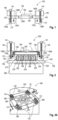
- Figure 1 illustrates an exemplary cryostat socket 100 configured to hold an ion trap device 180 mounted on a front side 190A of a device carrier 190 in a cryostat (not shown).
- the ion trap device 180 may be a micro-fabricated ion trap device.
- the device carrier 190 may include a laterally inner region and a laterally outer region.
- the ion trap device 180 may be mounted on the front side 190A of the device carrier 190 in the laterally inner region thereof.
- the device carrier 190 may be configured to spread heat produced by the ion trap device 180 from the laterally inner region to the laterally outer region of the device carrier 190.
- the ion trap device 180 may be a micro-fabricated device, e.g. a chip.
- the lateral dimensions may, e.g., be 5 to 10 mm or more.
- the device carrier 190 may have lateral dimensions of, for example, a couple of cm.
- the cryostat socket 100 comprises a frame 130 and a cover 140.
- the frame 130 and the cover 140 together may form part of a housing accommodating the ion trap device 190.
- the frame 130 and the cover 140 may define a measurement cell (or measurement chamber).
- the frame 130 includes a heat removal surface 130A configured to be thermally coupled to the laterally outer region of the device carrier 190.
- the cover 140 can be assembled with the frame 130.
- the cover 140 is configured to exert a compressive force on the laterally outer region of the front side 190A of the device carrier 190 when assembled with the frame 130, by which the rear side 190B of the device carrier 190 is thermally coupled to the heat removal surface 130A.
- the cover 140 may be detachably secured to the frame 130 by screw connections 141.
- the frame 130 may be provided with threaded holes 137 configured to receive the screw connections 141. That way, the cover 140 may be detachably secured to the frame 130.
- the compressive force is exerted on the front side 190A of the device carrier 190 by abutment surfaces 140B of the cover 140.
- the abutment surfaces 140B may exert a high pressure on the laterally outer region of the device carrier 190 to create high thermal conductivity in the contact area between the device carrier 190 and the heat removal surface 130A.
- the pressure may exceed 200 N/mm 2 or 300 N/mm 2 , for example.
- the cover 140 may have a top side opening 142.
- FIG. 1 Arrows in Figure 1 illustrate the direction of heat flow from the ion trap device 180 through the device carrier 190 into the frame 130.
- the heat flow in the device carrier 190 is mainly in a lateral direction.
- the heat is then redirected mainly in the vertical direction when entering into and propagating in the frame 130.
- the cover 140 may act as a compression lid when assembled with the frame 130.
- the efficiency of heat removal from the device carrier 190 into the frame 130 is dependent on the amount of pressure exerted by the cover 140 on the device carrier 190.
- the frame 130 may be coupled to a cryogenic head (not shown in Figure 1 ) of the cryostat via one or a plurality of metal pressure contacts.
- the metal pressure contacts may be provided between pressure surfaces 130B of the frame 130 and counteracting pressure surfaces (not shown in Figure 1 ) of the cryogenic head.
- the cryostat socket 100 is used during operation in a cryogenic and vacuum environment.
- the cryogenic operation temperature may be, e.g., about 4 to 10K.
- An ultra-high vacuum (UHV) of, e.g., less than 10 -10 mbar may be applied.
- FIG. 2 illustrates a cryostat socket 200 which is similar to the cryostat socket 100, and reference is made to the above description to avoid reiteration.
- Figure 2 illustrates an example of the device carrier 190 in greater detail.
- the device carrier 190 may include a substrate 192 and a metal layer 194.
- the ion trap device 180 is thermally coupled to a radially inner region of the metal layer 194.
- the metal layer 194 is configured to dissipate heat produced by the ion trap device 180 to the laterally outer region of the device carrier 190.
- the substrate 192 may include or be made of an insulating material, e.g. a core material of a printed circuit board (PCB) or, e.g., ceramics.
- the substrate 192 may comprise or be of FR4 or RO4350 of Rogers Corporation or other low RF loss laminate.
- the substrate 192 may comprise or be of sapphire or ceramics such as, e.g., AlN.
- the metal layer 194 may, e.g., be disposed over the substrate 192 at the front side 190A of the device carrier 190.
- the device carrier 190 may include one or a plurality of metallic heat removal surfaces 196 arranged on the rear side 190B of the device carrier 190.
- the heat removal surfaces 196 of the device carrier 190 are configured to be thermally coupled to the one or plurality of heat removal surfaces 130A of the frame 130 by the pressure exerted by the cover 140.
- the substrate 192 comprises or is of a material with high thermal conductivity such as, e.g., ceramic or sapphire, the heat removal surfaces 196 may, in particular, be omitted.
- the one or more metallic heat removal surfaces 196 are thermally coupled to the metal layer 194.
- coupling may be provided by one or a plurality of thermal vias 198 passing through the substrate 192 in the outer region of the device carrier 190.
- the thermal vias 198 may, e.g., have a high area density to provide for an effective thermal connection between the front side 190A and the rear side 190B of the device carrier 190.
- the rear side 190B of the device carrier 190 may be provided with an array of contact pads 199.
- the contact pads 199 are connected to electrical terminals (not shown) of the ion trap device 180 via an electrical interconnect (not shown) provided in the device carrier 190.
- the electrical interconnect may be implemented by an electrical redistribution structure embedded in the substrate 192.
- a spring pin insert 210 may be arranged in the frame 130.
- the spring pin insert 210 may include a base plate 220 and contact pins 230 resiliently received in the base plate 220.
- the contact pins 230 may be arranged in an array. When assembled, the array of contact pads 199 at the rear side 190B of the device carrier 190 contact the array of contact pins 230.
- the contact pins 230 are slightly depressed in their spring seats when the cover 140 is fixedly secured to the frame 130. This ensures a reliable electrical contact between the spring pin insert 210 and the device carrier 190 over a wide temperature range.
- the spring pin insert 210 may comprise or be made of a material having a similar CTE (coefficient of thermal expansion) as the substrate 192. This reduces lateral displacement between these parts during temperature cycling.
- the spring pin insert 210 may include or be made of one of the materials cited above for the substrate 192.
- the spring pin insert 210 may include or be made of the same material as the substrate 192.
- Figure 2 further illustrates an (optional) application board 250.
- the application board 250 may comprise an electrical wiring for electrically connecting the contact pins 230 of the spring pin insert 210 at their bottom region.
- conductive structures 252 on the application board 250 may be routed into the inside of the frame and may be connected to the contact pins 230 of the spring pin insert 210.
- the electrical wiring (e.g. conductive structures 252) of the application board 250 may connect the contact pins 230 of the spring pin insert 210 with electrical circuitry and/or electrical components (not shown) implemented laterally outside the frame 130 on the application board 250, for example.
- the frame 130 is configured to be thermally attached to a cryogenic head 280 of the cryostat via one or a plurality of metal pressure contacts (not shown in Figure 2 ).
- the frame 130 may be an integral part of the cryogenic head 280 of a cryostat.
- the coupling of the frame 130 to a cryogenic head of the cryostat should, in all examples, be as good as possible in terms of thermal connectivity in order to allow for highly efficient heat transfer.
- all solid state interfaces, if any, between the frame 130 and a cryogenic head 280 of the cryostat are implemented by metal pressure contacts.
- the cryogenic head 280 forms a cooled mounting platform of the cryostat.
- the heat generated by the ion trap device 180 is effectively conducted to the outer region of the device carrier 190. From the outer region of the device carrier 190 the heat is effectively conducted to the frame 130. The heat is then effectively conducted from the frame 130 to the cryostat head 280 either by using a frame 130 which is integral with the cryostat head 280 or by using metal pressure contacts between the cryostat head 280 and the frame 130.
- FIGS 3A-3E illustrate various stages of assembly of a cryostat socket 300.
- the cryostat socket 300 exhibits various features and variations of the cryostat sockets 100, 200, and reference is made to the above description to avoid reiteration.
- Figure 3A illustrates optional elements of the cryogenic socket 300, on which the frame 130 may be mounted.
- Reference sign 382 indicates pressure surfaces of a support plate 380 (see Figure 5 ) of the cryostat socket 300.
- the pressure surfaces 382 are configured to be pressed against the pressure surfaces 130B of the frame 130 by virtue of screw connections 131, for example.
- the pressure surfaces 382 may, e.g., be arranged opposite to corners of the frame 130.
- heat generated in the ion trap device 180 is removed from the frame 130 through the (e.g., four) pressure surfaces 382.
- the support plate 380 may be mounted on the cryostat head, or the pressure surfaces 382 may form surfaces of the cryogenic head itself (i.e., the support plate 380 may be omitted).
- Figure 3A further illustrates conductive structures 252 of the application board 250 located in a region of the application board 250 over which the spring pin insert 210 is to be placed.
- the conductive structures 252 are, e.g., formed by pads or conductive traces on the application board 250.
- the application board 250 as well as the support plate 380 may include an opening 384.
- the opening 384 provides for access (e.g. optical access, neutral atoms access, etc.) to the ion trap device 180.
- the support plate 380 (see Figure 5 ) or any other base part to which the frame 130 is mounted may further be equipped with guide means 132.
- the guide means 132 are configured to adjust the location of the frame 130 relative to the application board 250 and thus, relative to the conductive structures 252 of the application board.
- the guide means 132 may be formed by guide pins configured to interact with corresponding guide holes provided in the frame 130.
- the application board 250 may, e.g., fixedly attached to the support plate 380.
- the frame 130 is fixedly secured to the support plate 380 (or directly to the cryogenic head 280 of the cryostat) by pressing the metal pressure contacts (pressure surfaces 130B and 382) together. This may be done, for example, by screw connections 131 that engage threaded holes in the support plate 380 (or in the cryogenic head 280 itself).
- the frame 130 may comprise a plurality of radially inwardly directed clamping projections with upwardly facing clamping surfaces 134.
- the clamping surfaces 134 may be located near clamping devices (e.g., threaded holes 137) included in the frame 130.
- the clamping surfaces 134 may form at least a part of the heat removal surface 130A of the frame 130 (see Figures 1, 2 ) .
- clamping surfaces 134 may be located near clamping devices (e.g., threaded holes 137) included in the frame 130 form at least a part of the heat removal surface 130A used to thermally couple to the rear side of the device carrier 190 by the compressive force when the device carrier 190 is assembled with the frame 130.
- clamping devices e.g., threaded holes 137
- two clamping projections 134 are provided per 90° circumferential sector of the frame 130. In other examples one or more than two projections may be provided per 90° circumferential sector of the frame 130 or a continuous clamping region extending along the inner edge of the frame 130 may be provided for heat removal.
- FIG 3C illustrates the cryostat socket 300 without cover 140.
- the carrier-mounted ion trap device 180 is not yet inserted in the frame 130.
- a spring pin insert 210 is arranged in the frame 130.
- the spring pin insert 210 provides an electrical connection between the conductive structures of the application board (or other electrical distribution/routing means) and electrical contacts on the rear side 190B of the device carrier 190.
- the spring pin insert 210 may include contact pins 230 resiliently accommodated in a base plate 220 of spring pin insert 210.
- the contact pins 230 may be arranged in an array.
- the lateral position of the spring pin insert 210 within the frame 130 is fixed by the frame 130.
- the spring pin insert 210 may be inserted into the frame 130 to be held in a laterally fixed position.
- the spring pin insert 210 may, e.g., have an outline 211 which matches, at least partially, to an outline of the inner edge of the frame 130.
- This outline 211 may include, for example, recesses that engage, for example, the clamping protrusions (with clamping surfaces 134) and/or other positioning structures (not shown) of the frame 130.
- the lateral position of the frame 130 may precisely define the lateral position of the spring pin insert 210. Consequently, the lateral position of the spring pin insert 210 may be defined by the guide means 132 used to adjust the position of the frame 130 relative to the application board 250.
- the spring pin insert 210 may include an opening 254.
- the opening 254 may be formed in a central portion of the spring pin insert 210.
- the opening 254 may be aligned with the opening 384 of the support plate 380.
- the spring pin insert 210 may further be provided with guide means 256 configured to cooperate with the device carrier 190 for fine adjustment of the lateral position of the device carrier 190 relative to the spring pin insert 210.
- the guide means 256 include guide pins located, e.g., at corners of the spring pin insert 210.
- the guide means 256 at the spring pin insert 210 ensure fine adjustment between the device carrier 190 and the spring pin insert 210. That is, the device carrier 190, when lowered onto the spring pin insert 210, is moved in an exactly vertical direction without slipping sideways.
- guide means 132 for coarse adjustment
- guide means 256 for fine adjustment
- the combination of guide means 132 (for coarse adjustment) and guide means 256 provides highly precise control of the lateral position of the device carrier 190 (and thus the ion trap device 180) relative to the cryostat socket 300.
- the guide means 132 reduce the lateral play of the chip carrier 190 relative to the contact pins 230 which improves the repeatability of the contact forming process.
- the structural width of the electrical interconnect e.g., the conductive structures 252 and/or the pin array spacing of the spring pin insert 210) may be reduced.
- laser alignment is significantly easier and less time consuming after each replacement of the device carrier 190.
- the device carrier 190 is placed in the frame 130.
- the guide means (pins) 256 engage with corresponding guide means 191 (e.g. holes) in the device carrier 190.
- the rear side 190B of the device carrier 190 contacts the contact pins 230.
- the contact pins 230 are slightly depressed in their spring seats to ensure a reliable electrical contact over a wide temperature range.
- the device carrier 190 may include one or a plurality of zones 197 of high thermal conductivity in vertical direction.
- the zones 197 may be arranged in a peripheral region of the device carrier 190. As illustrated in Figure 3D , the zones 197 may be distributed along the perimeter of the chip carrier 190.
- the zones 197 may, e.g., be formed by thermal vias 198 (see Figure 2 ) and, optionally, continuous metallizations at the front surface 190A and/or the rear surface 190B of the device carrier 190.
- a zone 197 may include or be formed of a bulk metal inlay reaching through the substrate 192.
- zones 197 may be aligned with the clamping surfaces 134 of the frame 130 to form a part of the heat removal path from the ion trap device 180 to the cryogenic head 280.
- the thermal conductivity of zone 197 may be greater than that of the device carrier material at cryogenic temperatures.
- copper having a thermal conductivity greater than, e.g., 100 W/m/K may be used, optionally gold plated for lower thermal interface resistance.
- the zones 197 may, e.g., comprise or be of gold, silver, AlN, or AlO.
- the device carrier 190 may further comprise a metal layer 194 through which the heat from ion trap device 180 is transferred to the outer region of the device carrier 190, e.g. to the zones 197 of high thermal conductivity.
- this metal layer is not shown. It may either be embedded in the device carrier 190 or it may be provided at the front side 190A or the rear side 190B of the device carrier 190.
- FIG 3E the cover 140 has been fixed to the frame 130.
- a perspective bottom view of the cover 140 is shown in Figure 4 .
- the cover 140 may be provided with a receptacle 148 for the device carrier 190.
- the receptacle 148 serves as holding means for the device carrier 190 when the device carrier 190 with the ion trap device 180 is loaded into the cover 140 and transferred to the partially pre-assembled cryostat socket 300, as, e.g., shown in Figure 3C .
- the cover 140 is used to hold the ion trap module during assembly, e.g., overhead assembly, facilitating replacement of the ion trap modules.
- the receptacle 148 is configured to exert a compressive force on the front side 190A of the device carrier 190. More specifically, the compressive force may be exerted by abutment surfaces 140B pressing onto the zones 197 of high thermal conductivity on the device carrier 190. By this compressive force the rear side 190 (e.g., more specifically, the metallic heat removal surfaces 196 thereon) is pressed onto the heat removal surface(s) 130A of the frame 130. Concurrently, the rear side 190B of the device carrier 190 may also be pressed onto the contact pins 230 of the spring pin insert 210.
- the compressive force may be exerted by abutment surfaces 140B pressing onto the zones 197 of high thermal conductivity on the device carrier 190.
- the rear side 190 e.g., more specifically, the metallic heat removal surfaces 196 thereon
- the rear side 190B of the device carrier 190 may also be pressed onto the contact pins 230 of the spring pin insert 210.
- the cover 140 may be designed in various different ways.
- the plurality of separate abutment surfaces 140B may be arranged at a distance from one another circumferentially on the cover 140.
- the cover 140 may be provided with at least one or two abutment surfaces 140B per 90° circumferential sector of the cover 140. In the example shown in Figure 4 , in total eight abutment surfaces 140B exist that form part of the receptacle 148 of the cover 140.
- the cover 140 may also provide for a high degree of vertical and/or lateral optical access to the ion trap device 180.
- each abutment surface 140B may be formed by a side wall element 144 of the cover 140.
- the side wall elements 144 may be separated from each other by cutouts 146 of the side wall of the cover 140.
- the cover 140 may have a cutout 146 at some or each side of the cover 140.
- the cover 140 may have cutouts 146 at some or each corner region of the cover 140.
- cutouts 146 are provided both at the side faces and the corner regions of the cover 140. That way, the side wall of the cover 140 is subdivided by, e.g., eight cutouts 146.
- the cutouts 146 may allow optical access to the ion trap device 180 from some or all side faces and/or corner regions of the cryostat socket 300.
- the numerical aperture NA may be equal to or greater than 0.1, 0.3, or 0.5.
- the receptacle 148 may, e.g., further include inner side faces 143.
- the inner side faces 143 may coarsely control the lateral position of the device carrier 190 when placed in the receptacle 148 of the cover 140.
- inner side faces 143 are provided on each side wall element 144 and are formed as vertical steps extending from the horizontal abutment surfaces 140B.
- the compressive force exerted by the cover 140 on the front side 190A of the device carrier 190 may be the only force applied to the front side 190A of the device carrier 190 to hold the device carrier 190 in place when assembled with the frame 130.
- the clamping of the device carrier 190 between the cover 140 and the frame 130 may be the only substantial heat removal path between the ion trap device 180 and the cryogenic head 280.
- one or more further heat removal paths such as, e.g., a central heat removal stamp (not shown) protruding through the opening 254 in the spring pin insert 210 and, e.g., through the opening 384 in the support plate 380 may be provided for additional heat removal.
- the screw connections 141 may pass through through-holes in some or all of the wall elements 144. By tightening the screw connections 141, the cover 140 is pressed onto the device carrier 190.
- the cover 140 may thus be referred to as a compression lid for device carrier cooling.
- the frame 130 and/or the cover 140 may comprise or be made of a material having a high thermal conductivity, e.g. copper, copper alloys, silver, sapphire, aluminum-nitrite or gold.
- the frame 130 and/or the cover 140 may be covered with a chemically inert layer of high thermal conductivity like for example platinum or gold to prevent oxidation and facilitate reliable thermal contacts along the heat-conducting path.
- Figure 5 is a sectional side view representation of the cryostat socket 300.
- the device carrier 190 may be provided with a landing pad 195 on the front side 190A thereof.
- the top side opening 142 of the cover 140 may be covered by a metal mesh 610.
- the metal mesh 610 may be a framed mesh, i.e. may be suspended at a mesh frame 612.
- the metal mesh 610 may be electrically insulated from the cover 140.
- the mesh frame 612 may, e.g., be of an electrically insulating material.
- the cryostat socket 300 may further include means configured for biasing the metal mesh 610 to an electrical potential different from the electrical potential of the cover.
- the cover 140 may include a contact pin 620 protruding in a direction towards the device carrier 190. More specifically, the contact pin 620 may contact the landing pad 195 of the device carrier 190 when the cover 140 is assembled with the frame 130.
- the contact pin 620 may, e.g., be mounted at the mesh frame 612 and is electrically connected to the metal mesh 610.
- the metal mesh 612 may, e.g., be transparent.
- the metal mesh 610 may be implemented by a transparent gold grid.
- the metal mesh 610 may allow to shield stray charges on the cryostat socket 300 or on cryostat windows as far as possible. In some examples the metal mesh 610 may be grounded. In other examples a user-selectable (none-zero) electrical potential can be applied to the metal mesh 610.
- a cover 140 of any cryostat socket for holding an ion trap device 180 mounted on a device carrier 190 in a cryostat is described.
- the cover 140 includes an opening (e.g. top side opening 142 and/or side wall cutouts 146) covered by a metal mesh, the metal mesh being electrically insulated from the cover 140.
- the cover 140 comprises means for biasing the metal mesh 610 to an electrical potential different from the electrical potential of the cover 140.
- such cover 140 with the metal mesh (e.g., metal mesh 610) may be used for any cryostat socket, i.e. also for cryostat sockets which use different heat dissipation concepts as described herein.
- FIGS 7 and 8 illustrate examples of ion trap modules 700, 800.
- the ion trap modules 700, 800 are suitable for being used in the cryostat sockets 100, 200, 300 described above, for example.
- the ion trap module 700 includes the micro-fabricated ion trap device 180 mounted in a laterally inner region on the front side 190A of the device carrier 190.
- the device carrier 190 may comprise the metal layer 194 and the substrate 192.
- the ion trap device 180 is thermally coupled to a radially inner region of the metal layer 194.
- the metal layer 194 is configured to dissipate heat produced by the ion trap device 180 to the laterally outer region of the device carrier 190.
- the device carrier 190 is provided with means for transferring heat from the outer region of the metal layer 194 through the substrate 192 to metallic heat removal surfaces 196 at the rear side 190B of the device carrier 190.
- the metal layer 194 is provided at the front side 190A of the device carrier 190.
- the metal layer 194 may be provided at the rear side 190B of the device carrier 190.
- the metallic heat removal surfaces 196 may, e.g., form an integral part of the metal layer 194.
- the heat transfer through the substrate 192 may be carried out in a central part of the device carrier 190 beneath the ion trap device 180 by, e.g. thermal vias 198.
- the metal layer 194 may, e.g., be implemented as an inner layer of the substrate 192. Further, multiple metal layers 194 may be used for heat dissipation, e.g. front side and/or back side and/or inner metal layers 194 in arbitrary combination. Moreover, the metal layer(s) 194 may be structured in a region beneath the ion trap device 180 to allow an electrical interconnect (not shown) formed in or on the substrate 192 to electrically connect to the ion trap device 180 (which may, e.g., a surface mount device or a device connected by bonding wires (not shown) to such electrical interconnect).
- an electrical interconnect not shown
- the (main) heat conduction path in the cryostat socket 100, 200, 300 may, e.g., include some or all of the elements 180 (ion trap device) -> 194 (metal layer) and/or 190 (device carrier) -> 197 (zone of high thermal conductivity of the device carrier) -> 196 (metallic heat removal surface on the device carrier) and/or 190B (rear side of the device carrier) -> 134 (clamping surface of frame) -> 130 (frame) -> 382 (pressure surface of base plate) -> 380 (base plate), with the respective intermediate pressure contacts as described above in connection with Figures 1 to 8 .
- an additional heat removal link may be provided such as by a heat bypass configured to thermally connect the cover 140 to the frame 130 or to any element in the aforementioned heat conduction path between the frame 130 and the base plate 380.
- a heat bypass configured to thermally connect the cover 140 to the frame 130 or to any element in the aforementioned heat conduction path between the frame 130 and the base plate 380.
- Such an additional heat removal link may be implemented, for example, by a screwable metal braid (e.g. copper) that can be screwed to the cover 140 and at least one of the aforementioned elements. If such heat bypass is implemented, a substantial part of the heat may also be transported via the heat bypass to the frame 130 or any element in the heat conduction path downstream the frame 130. This may add heat removal capacity and/or allow to reduce the heat removal capacity via the rear side 190B of the device carrier 190 to the heat removal surface 130A of the frame 130.
- Figure 9 illustrates simulation results of the surface temperature of the ion trap device 180 as a function of the thickness of a metal layer 194 that comprises copper.
- Curve 910 relates to a first copper specimen having a thermal conductivity of 400 W/m/K
- curve 920 relates to a second copper specimen having a thermal conductivity of 1,540 W/m/K.
- T ⁇ 20K may be achieved from a minimum thickness of, e.g., 200 um (for copper of a typical thermal conductivity, see curve 910) or 100 ⁇ m (for copper of a specifically high thermal conductivity, see curve 920).
- the metal layer 194 may have a minimum thickness of equal to or greater than 100 ⁇ m or 200 ⁇ m or 300 ⁇ m or 400 ⁇ m or 500 ⁇ m, for example. In some examples, the thickness of the metal layer 194 may, e.g., be in a range between 200 ⁇ m and 600 ⁇ m. If the device carrier 190 includes or is of a high thermally conductive material such as, e.g., ceramic or sapphire, the metal layer 194 may be much thinner or even omitted.
Landscapes
- Engineering & Computer Science (AREA)
- Physics & Mathematics (AREA)
- General Engineering & Computer Science (AREA)
- Chemical & Material Sciences (AREA)
- Combustion & Propulsion (AREA)
- Mechanical Engineering (AREA)
- Thermal Sciences (AREA)
- Spectroscopy & Molecular Physics (AREA)
- High Energy & Nuclear Physics (AREA)
- Plasma & Fusion (AREA)
- Analytical Chemistry (AREA)
- Cooling Or The Like Of Electrical Apparatus (AREA)
Abstract
A cryostat socket for holding an ion trap device mounted on a substrate in a cryostat comprises a frame having a heat removal surface configured to be thermally coupled to a laterally outer region of the device carrier. The cryostat socket further comprises a cover configured to exert a compressive force on the front side of the device carrier when assembled with the frame, by which the rear side of the device carrier is thermally coupled to the heat removal surface.
Description
- This disclosure relates generally to the field of ion traps, and in particular to ion traps for quantum computing installed in a cryogenic environment.
- Trapped ions are one of the most promising candidates for use as qubits (quantum bits) in quantum computers since they can be trapped with long lifetimes in a scalable array by virtue of electromagnetic fields.
- Ion trap devices are operated in a cryogenic environment. To that end, an ion trap device is mechanically and thermally coupled to a cryostat head by means of a cryostat socket. The design of the cryostat socket significantly affects the performance of the ion trap device.
- Future ion trap devices may need to increase the number of controllable ions. As a consequence, the ion trap devices may increase in size. Further, the number of trap electrodes and the power dissipation of ion trap devices may increase..
- The cryostat socket may allow optical access from a plurality of sides with a suitable numerical aperture. Further, the exposure of ions (or qubits) to electrostatic potentials due to contamination or optically generated stray charges should be as low as possible.
- Moreover, a cryostat socket may allow safe and fast ion trap device changes for short learning cycles in further development. Typically, ion trap device changes are complicated because the ion trap devices need to be installed and removed upright or overhead, usually in very confined spaces.
- According to an aspect of the disclosure, a cryostat socket for holding an ion trap device mounted on a front side of a device carrier in a cryostat comprises a frame having a heat removal surface configured to be thermally coupled to a laterally outer region of the device carrier. The cryostat socket further comprises a cover configured to exert a compressive force on the front side of the device carrier when assembled with the frame, by which the rear side of the device carrier is thermally coupled to the heat removal surface.
- According to another aspect of the disclosure, an ion trap module comprises a device carrier having a laterally inner region and a laterally outer region. A micro-fabricated ion trap device is mounted in the laterally inner region on a front side of the device carrier. The device carrier is configured to spread heat produced by the ion trap device from the laterally inner region to the laterally outer region.
- Like reference numerals designate corresponding similar parts. The features of the various illustrated embodiments can be combined unless they exclude each other and/or can be selectively omitted if not described to be necessarily required. Embodiments are depicted in the drawings and are exemplarily detailed in the description which follows.
-
Figure 1 is a schematic cross-sectional view of an exemplary cryostat socket. -
Figure 2 is a schematic cross-sectional view of an exemplary cryostat socket having a spring pin insert arranged within a frame of the cryostat socket. -
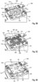
Figure 3A is a perspective top view illustrating exemplary metal pressure contacts of a cryogenic head. -
Figure 3B is the perspective top view ofFigure 3A with an exemplary cryostat socket frame mounted to the cryogenic head. -
Figure 3C is the perspective top view ofFigure 3B with an exemplary spring pin insert placed in the cryostat socket frame. -
Figure 3D is the perspective top view ofFigure 3C with an exemplary ion trap module disposed over the spring pin insert within the cryostat socket frame. -
Figure 3E is the perspective top view ofFigure 3D with an exemplary cover assembled with the frame. -
Figure 4 is a perspective bottom view of an exemplary cover of the cryostat socket with an ion trap module disposed in the cover. -
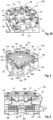
Figure 5 is a cutaway perspective view along line A-A ofFigure 3E . -
Figure 6A is the perspective top view ofFigure 3E with an exemplary metal mesh covering an opening of the cover. -
Figure 6B is the cutaway perspective view ofFigure 5 with the exemplary metal mesh ofFigure 6A assembled with the cover. -
Figure 7 is a schematic sectional view of an exemplary ion trap module having a device carrier which includes a substrate and a metal layer. -
Figure 8 is a schematic sectional view of another exemplary ion trap module having a device carrier which includes a substrate and a metal layer. -
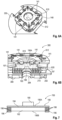
Figure 9 is a diagram illustrating the surface temperature of the ion trap device as a function of the thickness of a metal layer of copper on the device carrier. - The words "over" or "on" or "beneath" with regard to a part, element or material layer formed or located or disposed or arranged or placed "over" or "on" or "beneath" a surface may be used herein to mean that the part, element or material layer be located (e.g. placed, formed, arranged, disposed, placed, etc.) "directly on" or "directly under", e.g. in direct contact with, the implied surface. The word "over" or "on" or "beneath" used with regard to a part, element or material layer formed or located or disposed or arranged or placed "over" or "on" or "beneath" a surface may, however, either be used herein to mean that the part, element or material layer be located (e.g. placed, formed, arranged, deposited, etc.) "indirectly on" or "indirectly under" the implied surface, with one or more additional parts, elements or layers being arranged between the implied surface and the part, element or material layer.
-
Figure 1 illustrates anexemplary cryostat socket 100 configured to hold anion trap device 180 mounted on afront side 190A of adevice carrier 190 in a cryostat (not shown). Theion trap device 180 may be a micro-fabricated ion trap device. - The
device carrier 190 may include a laterally inner region and a laterally outer region. Theion trap device 180 may be mounted on thefront side 190A of thedevice carrier 190 in the laterally inner region thereof. Thedevice carrier 190 may be configured to spread heat produced by theion trap device 180 from the laterally inner region to the laterally outer region of thedevice carrier 190. - The
ion trap device 180 may be a micro-fabricated device, e.g. a chip. The lateral dimensions may, e.g., be 5 to 10 mm or more. Thedevice carrier 190 may have lateral dimensions of, for example, a couple of cm. - The
cryostat socket 100 comprises aframe 130 and acover 140. Theframe 130 and thecover 140 together may form part of a housing accommodating theion trap device 190. As will be described in greater detail further below, theframe 130 and thecover 140 may define a measurement cell (or measurement chamber). - The
frame 130 includes aheat removal surface 130A configured to be thermally coupled to the laterally outer region of thedevice carrier 190. Thecover 140 can be assembled with theframe 130. Thecover 140 is configured to exert a compressive force on the laterally outer region of thefront side 190A of thedevice carrier 190 when assembled with theframe 130, by which therear side 190B of thedevice carrier 190 is thermally coupled to theheat removal surface 130A. - For example, the
cover 140 may be detachably secured to theframe 130 byscrew connections 141. Theframe 130 may be provided with threadedholes 137 configured to receive thescrew connections 141. That way, thecover 140 may be detachably secured to theframe 130. When assembled with theframe 130 by, e.g., tightening the screw connections 141 (seeFigure 1 ), the compressive force is exerted on thefront side 190A of thedevice carrier 190 byabutment surfaces 140B of thecover 140. Theabutment surfaces 140B may exert a high pressure on the laterally outer region of thedevice carrier 190 to create high thermal conductivity in the contact area between thedevice carrier 190 and theheat removal surface 130A. The pressure may exceed 200 N/mm2 or 300 N/mm2, for example. - As will be describe in more detail further below, the
cover 140 may have a top side opening 142. - Arrows in
Figure 1 illustrate the direction of heat flow from theion trap device 180 through thedevice carrier 190 into theframe 130. The heat flow in thedevice carrier 190 is mainly in a lateral direction. The heat is then redirected mainly in the vertical direction when entering into and propagating in theframe 130. - In other words, the
cover 140 may act as a compression lid when assembled with theframe 130. The efficiency of heat removal from thedevice carrier 190 into theframe 130 is dependent on the amount of pressure exerted by thecover 140 on thedevice carrier 190. - The
frame 130 may be coupled to a cryogenic head (not shown inFigure 1 ) of the cryostat via one or a plurality of metal pressure contacts. The metal pressure contacts may be provided between pressure surfaces 130B of theframe 130 and counteracting pressure surfaces (not shown inFigure 1 ) of the cryogenic head. - Typically, the
cryostat socket 100 is used during operation in a cryogenic and vacuum environment. The cryogenic operation temperature may be, e.g., about 4 to 10K. An ultra-high vacuum (UHV) of, e.g., less than 10-10 mbar may be applied. -
Figure 2 illustrates acryostat socket 200 which is similar to thecryostat socket 100, and reference is made to the above description to avoid reiteration.Figure 2 illustrates an example of thedevice carrier 190 in greater detail. Thedevice carrier 190 may include asubstrate 192 and ametal layer 194. Theion trap device 180 is thermally coupled to a radially inner region of themetal layer 194. Themetal layer 194 is configured to dissipate heat produced by theion trap device 180 to the laterally outer region of thedevice carrier 190. - The
substrate 192 may include or be made of an insulating material, e.g. a core material of a printed circuit board (PCB) or, e.g., ceramics. For example, thesubstrate 192 may comprise or be of FR4 or RO4350 of Rogers Corporation or other low RF loss laminate. Further, thesubstrate 192 may comprise or be of sapphire or ceramics such as, e.g., AlN. Themetal layer 194 may, e.g., be disposed over thesubstrate 192 at thefront side 190A of thedevice carrier 190. - The
device carrier 190 may include one or a plurality of metallic heat removal surfaces 196 arranged on therear side 190B of thedevice carrier 190. The heat removal surfaces 196 of thedevice carrier 190 are configured to be thermally coupled to the one or plurality of heat removal surfaces 130A of theframe 130 by the pressure exerted by thecover 140. If thesubstrate 192 comprises or is of a material with high thermal conductivity such as, e.g., ceramic or sapphire, the heat removal surfaces 196 may, in particular, be omitted. - The one or more metallic heat removal surfaces 196 are thermally coupled to the
metal layer 194. For example, coupling may be provided by one or a plurality ofthermal vias 198 passing through thesubstrate 192 in the outer region of thedevice carrier 190. Thethermal vias 198 may, e.g., have a high area density to provide for an effective thermal connection between thefront side 190A and therear side 190B of thedevice carrier 190. - As illustrated in
Figure 2 , therear side 190B of thedevice carrier 190 may be provided with an array ofcontact pads 199. Thecontact pads 199 are connected to electrical terminals (not shown) of theion trap device 180 via an electrical interconnect (not shown) provided in thedevice carrier 190. For example, the electrical interconnect may be implemented by an electrical redistribution structure embedded in thesubstrate 192. - As illustrated in
Figure 2 , aspring pin insert 210 may be arranged in theframe 130. Thespring pin insert 210 may include abase plate 220 and contact pins 230 resiliently received in thebase plate 220. - The contact pins 230 may be arranged in an array. When assembled, the array of
contact pads 199 at therear side 190B of thedevice carrier 190 contact the array of contact pins 230. The contact pins 230 are slightly depressed in their spring seats when thecover 140 is fixedly secured to theframe 130. This ensures a reliable electrical contact between thespring pin insert 210 and thedevice carrier 190 over a wide temperature range. - The
spring pin insert 210 may comprise or be made of a material having a similar CTE (coefficient of thermal expansion) as thesubstrate 192. This reduces lateral displacement between these parts during temperature cycling. In particular, thespring pin insert 210 may include or be made of one of the materials cited above for thesubstrate 192. In particular, thespring pin insert 210 may include or be made of the same material as thesubstrate 192. -
Figure 2 further illustrates an (optional)application board 250. Theapplication board 250 may comprise an electrical wiring for electrically connecting the contact pins 230 of thespring pin insert 210 at their bottom region. To this end,conductive structures 252 on theapplication board 250 may be routed into the inside of the frame and may be connected to the contact pins 230 of thespring pin insert 210. The electrical wiring (e.g. conductive structures 252) of theapplication board 250 may connect the contact pins 230 of thespring pin insert 210 with electrical circuitry and/or electrical components (not shown) implemented laterally outside theframe 130 on theapplication board 250, for example. - The
frame 130 is configured to be thermally attached to acryogenic head 280 of the cryostat via one or a plurality of metal pressure contacts (not shown inFigure 2 ). In other examples, as e.g. illustrated inFigure 2 , theframe 130 may be an integral part of thecryogenic head 280 of a cryostat. The coupling of theframe 130 to a cryogenic head of the cryostat should, in all examples, be as good as possible in terms of thermal connectivity in order to allow for highly efficient heat transfer. Typically, all solid state interfaces, if any, between theframe 130 and acryogenic head 280 of the cryostat are implemented by metal pressure contacts. Thecryogenic head 280 forms a cooled mounting platform of the cryostat. - In other words, the heat generated by the
ion trap device 180 is effectively conducted to the outer region of thedevice carrier 190. From the outer region of thedevice carrier 190 the heat is effectively conducted to theframe 130. The heat is then effectively conducted from theframe 130 to thecryostat head 280 either by using aframe 130 which is integral with thecryostat head 280 or by using metal pressure contacts between thecryostat head 280 and theframe 130. -
Figures 3A-3E illustrate various stages of assembly of acryostat socket 300. Thecryostat socket 300 exhibits various features and variations of thecryostat sockets -
Figure 3A illustrates optional elements of thecryogenic socket 300, on which theframe 130 may be mounted.Reference sign 382 indicates pressure surfaces of a support plate 380 (seeFigure 5 ) of thecryostat socket 300. The pressure surfaces 382 are configured to be pressed against the pressure surfaces 130B of theframe 130 by virtue ofscrew connections 131, for example. The pressure surfaces 382 may, e.g., be arranged opposite to corners of theframe 130. In the example shown inFigure 3A heat generated in theion trap device 180 is removed from theframe 130 through the (e.g., four) pressure surfaces 382. Thesupport plate 380 may be mounted on the cryostat head, or the pressure surfaces 382 may form surfaces of the cryogenic head itself (i.e., thesupport plate 380 may be omitted). -
Figure 3A further illustratesconductive structures 252 of theapplication board 250 located in a region of theapplication board 250 over which thespring pin insert 210 is to be placed. Theconductive structures 252 are, e.g., formed by pads or conductive traces on theapplication board 250. - The
application board 250 as well as thesupport plate 380 may include anopening 384. Theopening 384 provides for access (e.g. optical access, neutral atoms access, etc.) to theion trap device 180. - The support plate 380 (see
Figure 5 ) or any other base part to which theframe 130 is mounted may further be equipped with guide means 132. The guide means 132 are configured to adjust the location of theframe 130 relative to theapplication board 250 and thus, relative to theconductive structures 252 of the application board. For example, the guide means 132 may be formed by guide pins configured to interact with corresponding guide holes provided in theframe 130. Theapplication board 250 may, e.g., fixedly attached to thesupport plate 380. - Referring to
Figure 3B , theframe 130 is fixedly secured to the support plate 380 (or directly to thecryogenic head 280 of the cryostat) by pressing the metal pressure contacts (pressure surfaces 130B and 382) together. This may be done, for example, byscrew connections 131 that engage threaded holes in the support plate 380 (or in thecryogenic head 280 itself). - The
frame 130 may comprise a plurality of radially inwardly directed clamping projections with upwardly facing clamping surfaces 134. The clamping surfaces 134 may be located near clamping devices (e.g., threaded holes 137) included in theframe 130. The clamping surfaces 134 may form at least a part of theheat removal surface 130A of the frame 130 (seeFigures 1, 2 ) . - In other words, the clamping surfaces 134 may be located near clamping devices (e.g., threaded holes 137) included in the
frame 130 form at least a part of theheat removal surface 130A used to thermally couple to the rear side of thedevice carrier 190 by the compressive force when thedevice carrier 190 is assembled with theframe 130. - In the example shown in
Figure 3B two clampingprojections 134 are provided per 90° circumferential sector of theframe 130. In other examples one or more than two projections may be provided per 90° circumferential sector of theframe 130 or a continuous clamping region extending along the inner edge of theframe 130 may be provided for heat removal. -
Figure 3C illustrates thecryostat socket 300 withoutcover 140. The carrier-mountedion trap device 180 is not yet inserted in theframe 130. Aspring pin insert 210 is arranged in theframe 130. Thespring pin insert 210 provides an electrical connection between the conductive structures of the application board (or other electrical distribution/routing means) and electrical contacts on therear side 190B of thedevice carrier 190. As already mentioned, thespring pin insert 210 may include contact pins 230 resiliently accommodated in abase plate 220 ofspring pin insert 210. As apparent fromFigure 3C , the contact pins 230 may be arranged in an array. - The lateral position of the
spring pin insert 210 within theframe 130 is fixed by theframe 130. For instance, thespring pin insert 210 may be inserted into theframe 130 to be held in a laterally fixed position. To this end, thespring pin insert 210 may, e.g., have anoutline 211 which matches, at least partially, to an outline of the inner edge of theframe 130. Thisoutline 211 may include, for example, recesses that engage, for example, the clamping protrusions (with clamping surfaces 134) and/or other positioning structures (not shown) of theframe 130. - In other words, the lateral position of the
frame 130 may precisely define the lateral position of thespring pin insert 210. Consequently, the lateral position of thespring pin insert 210 may be defined by the guide means 132 used to adjust the position of theframe 130 relative to theapplication board 250. - The
spring pin insert 210 may include anopening 254. Theopening 254 may be formed in a central portion of thespring pin insert 210. Theopening 254 may be aligned with theopening 384 of thesupport plate 380. - The
spring pin insert 210 may further be provided with guide means 256 configured to cooperate with thedevice carrier 190 for fine adjustment of the lateral position of thedevice carrier 190 relative to thespring pin insert 210. In the example shown inFigure 3C , the guide means 256 include guide pins located, e.g., at corners of thespring pin insert 210. The guide means 256 at thespring pin insert 210 ensure fine adjustment between thedevice carrier 190 and thespring pin insert 210. That is, thedevice carrier 190, when lowered onto thespring pin insert 210, is moved in an exactly vertical direction without slipping sideways. - The combination of guide means 132 (for coarse adjustment) and guide means 256 (for fine adjustment) provides highly precise control of the lateral position of the device carrier 190 (and thus the ion trap device 180) relative to the
cryostat socket 300. Moreover, the guide means 132 reduce the lateral play of thechip carrier 190 relative to the contact pins 230 which improves the repeatability of the contact forming process. As a result, the structural width of the electrical interconnect (e.g., theconductive structures 252 and/or the pin array spacing of the spring pin insert 210) may be reduced. Moreover, laser alignment is significantly easier and less time consuming after each replacement of thedevice carrier 190. - In
Figure 3D thedevice carrier 190 is placed in theframe 130. In this example, the guide means (pins) 256 engage with corresponding guide means 191 (e.g. holes) in thedevice carrier 190. - In its final position the
rear side 190B of thedevice carrier 190 contacts the contact pins 230. The contact pins 230 are slightly depressed in their spring seats to ensure a reliable electrical contact over a wide temperature range. - The
device carrier 190 may include one or a plurality ofzones 197 of high thermal conductivity in vertical direction. Thezones 197 may be arranged in a peripheral region of thedevice carrier 190. As illustrated inFigure 3D , thezones 197 may be distributed along the perimeter of thechip carrier 190. Thezones 197 may, e.g., be formed by thermal vias 198 (seeFigure 2 ) and, optionally, continuous metallizations at thefront surface 190A and/or therear surface 190B of thedevice carrier 190. In other examples, azone 197 may include or be formed of a bulk metal inlay reaching through thesubstrate 192. Thesezones 197 may be aligned with the clamping surfaces 134 of theframe 130 to form a part of the heat removal path from theion trap device 180 to thecryogenic head 280. The thermal conductivity ofzone 197 may be greater than that of the device carrier material at cryogenic temperatures. For example, copper having a thermal conductivity greater than, e.g., 100 W/m/K may be used, optionally gold plated for lower thermal interface resistance. In other examples, thezones 197 may, e.g., comprise or be of gold, silver, AlN, or AlO. - As mentioned above, the
device carrier 190 may further comprise ametal layer 194 through which the heat fromion trap device 180 is transferred to the outer region of thedevice carrier 190, e.g. to thezones 197 of high thermal conductivity. InFigure 3D this metal layer is not shown. It may either be embedded in thedevice carrier 190 or it may be provided at thefront side 190A or therear side 190B of thedevice carrier 190. - In
Figure 3E thecover 140 has been fixed to theframe 130. A perspective bottom view of thecover 140 is shown inFigure 4 . - The
cover 140 may be provided with areceptacle 148 for thedevice carrier 190. Thereceptacle 148 serves as holding means for thedevice carrier 190 when thedevice carrier 190 with theion trap device 180 is loaded into thecover 140 and transferred to the partiallypre-assembled cryostat socket 300, as, e.g., shown inFigure 3C . Thecover 140 is used to hold the ion trap module during assembly, e.g., overhead assembly, facilitating replacement of the ion trap modules. - Further, when the
cover 140 is assembled with theframe 130, thereceptacle 148 is configured to exert a compressive force on thefront side 190A of thedevice carrier 190. More specifically, the compressive force may be exerted byabutment surfaces 140B pressing onto thezones 197 of high thermal conductivity on thedevice carrier 190. By this compressive force the rear side 190 (e.g., more specifically, the metallic heat removal surfaces 196 thereon) is pressed onto the heat removal surface(s) 130A of theframe 130. Concurrently, therear side 190B of thedevice carrier 190 may also be pressed onto the contact pins 230 of thespring pin insert 210. - The
cover 140 may be designed in various different ways. For example, the plurality of separate abutment surfaces 140B may be arranged at a distance from one another circumferentially on thecover 140. For example, thecover 140 may be provided with at least one or twoabutment surfaces 140B per 90° circumferential sector of thecover 140. In the example shown inFigure 4 , in total eightabutment surfaces 140B exist that form part of thereceptacle 148 of thecover 140. - Besides its capacity to exert compressive force onto the
device carrier 190, thecover 140 may also provide for a high degree of vertical and/or lateral optical access to theion trap device 180. - For example, each
abutment surface 140B may be formed by aside wall element 144 of thecover 140. Theside wall elements 144 may be separated from each other bycutouts 146 of the side wall of thecover 140. In one example thecover 140 may have acutout 146 at some or each side of thecover 140. Alternatively or in addition, thecover 140 may havecutouts 146 at some or each corner region of thecover 140. InFigure 4 cutouts 146 are provided both at the side faces and the corner regions of thecover 140. That way, the side wall of thecover 140 is subdivided by, e.g., eightcutouts 146. Thecutouts 146 may allow optical access to theion trap device 180 from some or all side faces and/or corner regions of thecryostat socket 300. For example, the numerical aperture NA may be equal to or greater than 0.1, 0.3, or 0.5. - The
receptacle 148 may, e.g., further include inner side faces 143. The inner side faces 143 may coarsely control the lateral position of thedevice carrier 190 when placed in thereceptacle 148 of thecover 140. In the example shown inFigure 4 , inner side faces 143 are provided on eachside wall element 144 and are formed as vertical steps extending from the horizontal abutment surfaces 140B. - The compressive force exerted by the
cover 140 on thefront side 190A of thedevice carrier 190 may be the only force applied to thefront side 190A of thedevice carrier 190 to hold thedevice carrier 190 in place when assembled with theframe 130. Further, the clamping of thedevice carrier 190 between thecover 140 and theframe 130 may be the only substantial heat removal path between theion trap device 180 and thecryogenic head 280. Optionally, one or more further heat removal paths such as, e.g., a central heat removal stamp (not shown) protruding through theopening 254 in thespring pin insert 210 and, e.g., through theopening 384 in thesupport plate 380 may be provided for additional heat removal. - Referring to
Figures 3B-3E , thescrew connections 141 may pass through through-holes in some or all of thewall elements 144. By tightening thescrew connections 141, thecover 140 is pressed onto thedevice carrier 190. Thecover 140 may thus be referred to as a compression lid for device carrier cooling. - The
frame 130 and/or thecover 140 may comprise or be made of a material having a high thermal conductivity, e.g. copper, copper alloys, silver, sapphire, aluminum-nitrite or gold. Theframe 130 and/or thecover 140 may be covered with a chemically inert layer of high thermal conductivity like for example platinum or gold to prevent oxidation and facilitate reliable thermal contacts along the heat-conducting path. -
Figure 5 is a sectional side view representation of thecryostat socket 300. Thedevice carrier 190 may be provided with alanding pad 195 on thefront side 190A thereof. - Referring to
Figures 6A and 6B , the top side opening 142 of thecover 140 may be covered by ametal mesh 610. Themetal mesh 610 may be a framed mesh, i.e. may be suspended at amesh frame 612. Themetal mesh 610 may be electrically insulated from thecover 140. To that end, themesh frame 612 may, e.g., be of an electrically insulating material. - The
cryostat socket 300 may further include means configured for biasing themetal mesh 610 to an electrical potential different from the electrical potential of the cover. For example, thecover 140 may include acontact pin 620 protruding in a direction towards thedevice carrier 190. More specifically, thecontact pin 620 may contact thelanding pad 195 of thedevice carrier 190 when thecover 140 is assembled with theframe 130. Thecontact pin 620 may, e.g., be mounted at themesh frame 612 and is electrically connected to themetal mesh 610. - The
metal mesh 612 may, e.g., be transparent. For example, themetal mesh 610 may be implemented by a transparent gold grid. - The
metal mesh 610 may allow to shield stray charges on thecryostat socket 300 or on cryostat windows as far as possible. In some examples themetal mesh 610 may be grounded. In other examples a user-selectable (none-zero) electrical potential can be applied to themetal mesh 610. - According to one aspect of the disclosure, a
cover 140 of any cryostat socket for holding anion trap device 180 mounted on adevice carrier 190 in a cryostat is described. Thecover 140 includes an opening (e.g. top side opening 142 and/or side wall cutouts 146) covered by a metal mesh, the metal mesh being electrically insulated from thecover 140. Thecover 140 comprises means for biasing themetal mesh 610 to an electrical potential different from the electrical potential of thecover 140. In general,such cover 140 with the metal mesh (e.g., metal mesh 610) may be used for any cryostat socket, i.e. also for cryostat sockets which use different heat dissipation concepts as described herein. -
Figures 7 and8 illustrate examples ofion trap modules ion trap modules cryostat sockets - The
ion trap module 700 includes the micro-fabricatedion trap device 180 mounted in a laterally inner region on thefront side 190A of thedevice carrier 190. - Referring also to
Figure 2 , thedevice carrier 190 may comprise themetal layer 194 and thesubstrate 192. Theion trap device 180 is thermally coupled to a radially inner region of themetal layer 194. Themetal layer 194 is configured to dissipate heat produced by theion trap device 180 to the laterally outer region of thedevice carrier 190. As described before, thedevice carrier 190 is provided with means for transferring heat from the outer region of themetal layer 194 through thesubstrate 192 to metallic heat removal surfaces 196 at therear side 190B of thedevice carrier 190. - In
Figure 7 themetal layer 194 is provided at thefront side 190A of thedevice carrier 190. In other examples (e.g.Figure 8 ) themetal layer 194 may be provided at therear side 190B of thedevice carrier 190. In this case, the metallic heat removal surfaces 196 may, e.g., form an integral part of themetal layer 194. Further, in this and other cases, the heat transfer through thesubstrate 192 may be carried out in a central part of thedevice carrier 190 beneath theion trap device 180 by, e.g.thermal vias 198. - In other examples, the
metal layer 194 may, e.g., be implemented as an inner layer of thesubstrate 192. Further,multiple metal layers 194 may be used for heat dissipation, e.g. front side and/or back side and/orinner metal layers 194 in arbitrary combination. Moreover, the metal layer(s) 194 may be structured in a region beneath theion trap device 180 to allow an electrical interconnect (not shown) formed in or on thesubstrate 192 to electrically connect to the ion trap device 180 (which may, e.g., a surface mount device or a device connected by bonding wires (not shown) to such electrical interconnect). - Thus, the (main) heat conduction path in the
cryostat socket Figures 1 to 8 . Further, an additional heat removal link (not shown in the Figures) may be provided such as by a heat bypass configured to thermally connect thecover 140 to theframe 130 or to any element in the aforementioned heat conduction path between theframe 130 and thebase plate 380. Such an additional heat removal link may be implemented, for example, by a screwable metal braid (e.g. copper) that can be screwed to thecover 140 and at least one of the aforementioned elements. If such heat bypass is implemented, a substantial part of the heat may also be transported via the heat bypass to theframe 130 or any element in the heat conduction path downstream theframe 130. This may add heat removal capacity and/or allow to reduce the heat removal capacity via therear side 190B of thedevice carrier 190 to theheat removal surface 130A of theframe 130. -
Figure 9 illustrates simulation results of the surface temperature of theion trap device 180 as a function of the thickness of ametal layer 194 that comprises copper.Curve 910 relates to a first copper specimen having a thermal conductivity of 400 W/m/K, whilecurve 920 relates to a second copper specimen having a thermal conductivity of 1,540 W/m/K. The thicker thecopper layer 194, the better will be the thermal coupling of theion trap device 180 to the cryostat, and therefore theion trap device 180 temperature (e.g., chip temperature) will decrease. - Depending on the thermal conductivity of the copper, practicable surface temperatures of T < 20K may be achieved from a minimum thickness of, e.g., 200 um (for copper of a typical thermal conductivity, see curve 910) or 100 µm (for copper of a specifically high thermal conductivity, see curve 920). Hence, the
metal layer 194 may have a minimum thickness of equal to or greater than 100 µm or 200 µm or 300 µm or 400 µm or 500 µm, for example. In some examples, the thickness of themetal layer 194 may, e.g., be in a range between 200 µm and 600 µm. If thedevice carrier 190 includes or is of a high thermally conductive material such as, e.g., ceramic or sapphire, themetal layer 194 may be much thinner or even omitted. - The following examples pertain to further aspects of the disclosure:
- Example 1 is a cryostat socket for holding an ion trap device mounted on a front side of a device carrier in a cryostat. The cryostat socket comprises a frame having a heat removal surface configured to be thermally coupled to a laterally outer region of the device carrier. The cryostat socket further comprises a cover configured to exert a compressive force on the front side of the device carrier when assembled with the frame, by which the rear side of the device carrier is thermally coupled to the heat removal surface.
- In Example 2, the subject matter of Example 1 can optionally include wherein the frame is coupled to a cryogenic head of the cryostat via one or a plurality of metal pressure contacts.
- In Example 3, the subject matter of Example 1 or 2 can optionally include wherein the frame comprises a plurality of radially inwardly directed clamping projections with upwardly facing clamping surfaces which form at least a part of the heat removal surface.
- In Example 4, the subject matter of Example 3 can optionally include wherein at least one or two clamping projections are provided per 90° circumferential sector of the frame.
- In Example 5, the subject matter of any of the preceding Examples can optionally include wherein the cover comprises a pressure surface which is located opposite the heat removal surface of the frame when the cover is assembled with the frame, wherein the compressive force is exerted on the front side of the device carrier via the pressure surface.
- In Example 6, the subject matter of Example 5 can optionally include wherein the pressure surface comprises a plurality of clamping surfaces arranged at a distance from one another circumferentially on the cover.
- In Example 7, the subject matter of any of the preceding Examples can optionally include wherein the cover has a quadrangular or octagonal peripheral shape, and wherein a peripheral wall of the cover has a cutout on each of the four or eight sides.
- In Example 8, the subject matter of any of the preceding Examples can optionally further include a spring pin insert arranged in the frame, the spring pin insert comprising a base plate and contact pins resiliently received in the base plate.
- In Example 9, the subject matter of Example 8 can optionally include wherein the spring pin insert comprises guide means configured to cooperate with the device carrier for fine adjustment of the lateral position of the device carrier relative to the spring pin insert.
- In Example 10, the subject matter of any of the preceding Examples can optionally include wherein the cover comprises an opening covered by a metal mesh, the metal mesh being electrically insulated from the cover; and means for biasing the metal mesh to an electrical potential different from the electrical potential of the cover.
- In Example 11, the subject matter of Example 10 can optionally include wherein the means for biasing the metal mesh comprises a contact pin protruding in a direction towards the device carrier.
- Example 12 is an ion trap module, comprising: a device carrier having a laterally inner region and a laterally outer region; and a micro-fabricated ion trap device mounted in the laterally inner region on a front side of the device carrier, wherein the device carrier is configured to spread heat produced by the ion trap device from the laterally inner region to the laterally outer region.
- In Example 13, the subject matter of Example 12 can optionally further include wherein the device carrier comprises a substrate and a metal layer, wherein the ion trap device is thermally coupled to a radially inner region of the metal layer and the metal layer is configured to dissipate heat produced by the ion trap device to the laterally outer region of the device carrier.
- In Example 14, the subject matter of Example 13 can optionally further include wherein the metal layer has a thickness of equal to or greater than 100 µm.
- In Example 15, the subject matter of Example 13 or 14 can optionally further include wherein the device carrier comprises a metallic heat removal surface arranged on the rear side of the device carrier, the metallic heat removal surface is thermally coupled to the metal layer.
- In Example 16, the subject matter of any of Examples 12 to 15 can optionally further include wherein the device carrier comprises an array of electrical contact pads arranged on the rear side of the device carrier; and an electrical interconnect for connecting the electrical contact pads to the micro-fabricated ion trap device.
- Example 17 is a system including a cryostat socket of any of Examples 1 to 11 and an ion trap module of any of Examples 12 to 16.
- Example 18 is a cover of a cryostat socket for holding an ion trap device mounted on a device carrier in a cryostat, the cover comprising an opening covered by a metal mesh being electrically insulated from the cover, and means for biasing the metal mesh to an electrical potential different from the electrical potential of the cover.
- In Example 19, the subject matter of Example 18 can optionally further include wherein the means for biasing the metal mesh to the electrical potential comprise a contact pin protruding in a direction towards the device carrier.
- In Example 20, the subject matter of Example 18 or 19 can optionally further include wherein the means for biasing the metal mesh is configured to electrically contact a landing pad of the device carrier.
- In Example 21, the subject matter of any of the Examples 18 to 20 can optionally further include a mesh frame for suspending the metal mesh, wherein the means for biasing the metal mesh is mounted to the mesh frame.
- Example 22 is a cryostat socket for holding an ion trap device mounted on a front side of a device carrier in a cryostat. The cryostat socket comprises a frame and a base part to which the frame is mounted. The base part is provided with guide means configured to cooperate with the frame for adjustment of the lateral position of the frame relative to the base part.
- In Example 23, the subject matter of Example 22 can optionally include wherein the base part is a support plate of the cryostat socket.
- In Example 24, the subject matter of Example 22 or 23 can optionally include wherein the guide means provided at the base part comprise guide pins configured to interact with corresponding guide holes provided in the frame.
- In Example 25, the subject matter of any of Examples 22 to 24 can optionally include wherein the guide means provided at the base part are configured for coarse positional adjustment and the guide means of the spring pin insert are configured for fine positional adjustment of the device carrier.
- Although specific embodiments have been illustrated and described herein, it will be appreciated by those of ordinary skill in the art that a variety of alternate and/or equivalent implementations may be substituted for the specific embodiments shown and described without departing from the scope of the present invention. This application is intended to cover any adaptations or variations of the specific embodiments discussed herein. Therefore, it is intended that this invention be limited only by the claims and the equivalents thereof.
Claims (17)
- A cryostat socket for holding an ion trap device mounted on a front side of a device carrier in a cryostat, the cryostat socket comprising:a frame having a heat removal surface configured to be thermally coupled to a laterally outer region of the device carrier; anda cover configured to exert a compressive force on the front side of the device carrier when assembled with the frame, by which the rear side of the device carrier is thermally coupled to the heat removal surface.
- The cryostat socket of claim 1, wherein the frame is coupled to a cryogenic head of the cryostat via one or a plurality of metal pressure contacts.
- The cryostat socket of claim 1 or 2, wherein the frame comprises a plurality of radially inwardly directed clamping projections with upwardly facing clamping surfaces which form at least a part of the heat removal surface.
- The cryostat socket of claim 3, wherein at least one or two clamping projections are provided per 90° circumferential sector of the frame.
- The cryostat socket of any of the preceding claims, wherein the cover comprises a pressure surface which is located opposite the heat removal surface of the frame when the cover is assembled with the frame, wherein the compressive force is exerted on the front side of the device carrier via the pressure surface.
- The cryostat socket of claim 5, wherein the pressure surface comprises a plurality of clamping surfaces arranged at a distance from one another circumferentially on the cover.
- The cryostat socket of any of the preceding claims, wherein the cover has a quadrangular or octagonal peripheral shape, and wherein a peripheral wall of the cover has a cutout on each of the four or eight sides.
- The cryostat socket of any of the preceding claims, further comprising:
a spring pin insert arranged in the frame, the spring pin insert comprising a base plate and contact pins resiliently received in the base plate. - The cryostat socket of claim 8, wherein the spring pin insert comprises guide means configured to cooperate with the device carrier for fine adjustment of the lateral position of the device carrier relative to the spring pin insert.
- The cryostat socket of any of the preceding claims, wherein the cover comprises:an opening covered by a metal mesh, the metal mesh being electrically insulated from the cover; andmeans for biasing the metal mesh to an electrical potential different from the electrical potential of the cover.
- The cryostat socket of claim 10, wherein the means for biasing the metal mesh comprises a contact pin protruding in a direction towards the device carrier.
- An ion trap module, comprising:a device carrier having a laterally inner region and a laterally outer region; anda micro-fabricated ion trap device mounted in the laterally inner region on a front side of the device carrier, whereinthe device carrier is configured to spread heat produced by the ion trap device from the laterally inner region to the laterally outer region.
- The ion trap module of claim 12, wherein the device carrier comprises a substrate and a metal layer, wherein the ion trap device is thermally coupled to a radially inner region of the metal layer and the metal layer is configured to dissipate heat produced by the ion trap device to the laterally outer region of the device carrier.
- The ion trap module of claim 13, wherein the metal layer has a thickness of equal to or greater than 100 pm.
- The ion trap module of claim 13 or 14, wherein the device carrier comprises a metallic heat removal surface arranged on the rear side of the device carrier, the metallic heat removal surface is thermally coupled to the metal layer.
- The ion trap module of any of claims 12 to 15, wherein the device carrier comprises:an array of electrical contact pads arranged on the rear side of the device carrier; andan electrical interconnect for connecting the electrical contact pads to the micro-fabricated ion trap device.
- A system comprising a cryostat socket of any of claims 1 to 11 and an ion trap module of any of claims 12 to 16.
Priority Applications (3)
| Application Number | Priority Date | Filing Date | Title |
|---|---|---|---|
| EP23158423.6A EP4421422A1 (en) | 2023-02-24 | 2023-02-24 | A cryostat socket for holding an ion trap device mounted on a substrate in a cryostat |
| US18/437,366 US20240288213A1 (en) | 2023-02-24 | 2024-02-09 | Cryostat socket for holding an ion trap device mounted on a substrate in a cryostat |
| CN202410202155.7A CN118553597A (en) | 2023-02-24 | 2024-02-23 | Cryostat receptacle for holding an ion trap device mounted on a substrate in a cryostat |
Applications Claiming Priority (1)
| Application Number | Priority Date | Filing Date | Title |
|---|---|---|---|
| EP23158423.6A EP4421422A1 (en) | 2023-02-24 | 2023-02-24 | A cryostat socket for holding an ion trap device mounted on a substrate in a cryostat |
Publications (1)
| Publication Number | Publication Date |
|---|---|
| EP4421422A1 true EP4421422A1 (en) | 2024-08-28 |
Family
ID=85384427
Family Applications (1)
| Application Number | Title | Priority Date | Filing Date |
|---|---|---|---|
| EP23158423.6A Pending EP4421422A1 (en) | 2023-02-24 | 2023-02-24 | A cryostat socket for holding an ion trap device mounted on a substrate in a cryostat |
Country Status (3)
| Country | Link |
|---|---|
| US (1) | US20240288213A1 (en) |
| EP (1) | EP4421422A1 (en) |
| CN (1) | CN118553597A (en) |
Families Citing this family (1)
| Publication number | Priority date | Publication date | Assignee | Title |
|---|---|---|---|---|
| KR102876568B1 (en) * | 2024-03-15 | 2025-10-27 | 포항공과대학교 산학협력단 | Ion trap device |
Citations (3)
| Publication number | Priority date | Publication date | Assignee | Title |
|---|---|---|---|---|
| DE102019205183A1 (en) * | 2019-04-11 | 2020-10-15 | Robert Bosch Gmbh | Method of making an ion trap |
| EP3792956A1 (en) * | 2019-09-13 | 2021-03-17 | Honeywell International Inc. | Enclosure for ion trapping device |
| CN114358297A (en) * | 2020-09-30 | 2022-04-15 | 英飞凌科技奥地利有限公司 | Apparatus for controlling trapped ions and method of manufacturing the same |
-
2023
- 2023-02-24 EP EP23158423.6A patent/EP4421422A1/en active Pending
-
2024
- 2024-02-09 US US18/437,366 patent/US20240288213A1/en active Pending
- 2024-02-23 CN CN202410202155.7A patent/CN118553597A/en active Pending
Patent Citations (3)
| Publication number | Priority date | Publication date | Assignee | Title |
|---|---|---|---|---|
| DE102019205183A1 (en) * | 2019-04-11 | 2020-10-15 | Robert Bosch Gmbh | Method of making an ion trap |
| EP3792956A1 (en) * | 2019-09-13 | 2021-03-17 | Honeywell International Inc. | Enclosure for ion trapping device |
| CN114358297A (en) * | 2020-09-30 | 2022-04-15 | 英飞凌科技奥地利有限公司 | Apparatus for controlling trapped ions and method of manufacturing the same |
Also Published As
| Publication number | Publication date |
|---|---|
| US20240288213A1 (en) | 2024-08-29 |
| CN118553597A (en) | 2024-08-27 |
Similar Documents
| Publication | Publication Date | Title |
|---|---|---|
| US7951650B2 (en) | Thermal management of electronic devices | |
| US5014161A (en) | System for detachably mounting semiconductors on conductor substrate | |
| US4509096A (en) | Chip-carrier substrates | |
| JP2003533009A (en) | Double Storage Optoelectronic Package | |
| US20250323191A1 (en) | Device for controlling trapped ions including a substrate mounted on an application board | |
| US6101094A (en) | Printed circuit board with integrated cooling mechanism | |
| EP0245179B1 (en) | System for detachably mounting semiconductors on conductor substrate. | |
| WO2020225578A1 (en) | Heat removal from silicon photonics chip using a recessed side-by-side thermal dissipation layout | |
| US20250198686A1 (en) | System including an ion trap device arranged on a substrate | |
| CN110167316A (en) | The mounting structure of communication module and the communication module | |
| US20240288213A1 (en) | Cryostat socket for holding an ion trap device mounted on a substrate in a cryostat | |
| KR102461709B1 (en) | Immersion cooling temperature control method, system, and apparatus | |
| JP7833946B2 (en) | PCB assembly | |
| US10582611B2 (en) | Thermal management structures for optoelectronic modules | |
| EP0516875B1 (en) | Module for electronic package | |
| US6534860B2 (en) | Thermal transfer plate | |
| JPS62261199A (en) | Heat radiation structure of printed wiring board on ehich electronic parts are mounted | |
| KR20140063713A (en) | Electrical control device with moulded housing | |
| US10595441B1 (en) | Method and apparatus for separating a thermal load path from a structural load path in a circuit board environment | |
| JPS63261738A (en) | Electric component for carrying integrated circuit | |
| CA1293066C (en) | System for detachably mounting semi-conductors on conductor substrates | |
| US20220386508A1 (en) | Electronic component | |
| JP2024131597A (en) | Semiconductor Device | |
| KR101045342B1 (en) | Board of sealed system and heat dissipation structure for it | |
| CN121417985A (en) | A laser communication device |
Legal Events
| Date | Code | Title | Description |
|---|---|---|---|
| PUAI | Public reference made under article 153(3) epc to a published international application that has entered the european phase |
Free format text: ORIGINAL CODE: 0009012 |
|
| STAA | Information on the status of an ep patent application or granted ep patent |
Free format text: STATUS: THE APPLICATION HAS BEEN PUBLISHED |
|
| AK | Designated contracting states |
Kind code of ref document: A1 Designated state(s): AL AT BE BG CH CY CZ DE DK EE ES FI FR GB GR HR HU IE IS IT LI LT LU LV MC ME MK MT NL NO PL PT RO RS SE SI SK SM TR |
|
| STAA | Information on the status of an ep patent application or granted ep patent |
Free format text: STATUS: REQUEST FOR EXAMINATION WAS MADE |
|
| 17P | Request for examination filed |
Effective date: 20250130 |