EP4418512A1 - Switched mode power supply (smps) - Google Patents
Switched mode power supply (smps) Download PDFInfo
- Publication number
- EP4418512A1 EP4418512A1 EP24157051.4A EP24157051A EP4418512A1 EP 4418512 A1 EP4418512 A1 EP 4418512A1 EP 24157051 A EP24157051 A EP 24157051A EP 4418512 A1 EP4418512 A1 EP 4418512A1
- Authority
- EP
- European Patent Office
- Prior art keywords
- smps
- inductor current
- current
- inductor
- charging circuit
- Prior art date
- Legal status (The legal status is an assumption and is not a legal conclusion. Google has not performed a legal analysis and makes no representation as to the accuracy of the status listed.)
- Pending
Links
- 208000006011 Stroke Diseases 0.000 claims abstract description 62
- 238000001514 detection method Methods 0.000 claims abstract description 16
- 230000007423 decrease Effects 0.000 claims abstract description 5
- 239000003990 capacitor Substances 0.000 claims description 30
- 238000004804 winding Methods 0.000 claims description 7
- 230000008901 benefit Effects 0.000 description 10
- 238000010586 diagram Methods 0.000 description 10
- 230000003247 decreasing effect Effects 0.000 description 3
- 238000007599 discharging Methods 0.000 description 3
- 238000004519 manufacturing process Methods 0.000 description 3
- 238000013461 design Methods 0.000 description 2
- 238000012986 modification Methods 0.000 description 2
- 230000004048 modification Effects 0.000 description 2
- 238000012544 monitoring process Methods 0.000 description 2
- 102100038026 DNA fragmentation factor subunit alpha Human genes 0.000 description 1
- 101000950906 Homo sapiens DNA fragmentation factor subunit alpha Proteins 0.000 description 1
- 230000001276 controlling effect Effects 0.000 description 1
- 238000002955 isolation Methods 0.000 description 1
- 239000000463 material Substances 0.000 description 1
- 238000000034 method Methods 0.000 description 1
- 230000003071 parasitic effect Effects 0.000 description 1
- 238000012545 processing Methods 0.000 description 1
- 230000001105 regulatory effect Effects 0.000 description 1
- 230000001960 triggered effect Effects 0.000 description 1
Images





Classifications
-
- H—ELECTRICITY
- H02—GENERATION; CONVERSION OR DISTRIBUTION OF ELECTRIC POWER
- H02M—APPARATUS FOR CONVERSION BETWEEN AC AND AC, BETWEEN AC AND DC, OR BETWEEN DC AND DC, AND FOR USE WITH MAINS OR SIMILAR POWER SUPPLY SYSTEMS; CONVERSION OF DC OR AC INPUT POWER INTO SURGE OUTPUT POWER; CONTROL OR REGULATION THEREOF
- H02M3/00—Conversion of DC power input into DC power output
- H02M3/02—Conversion of DC power input into DC power output without intermediate conversion into AC
- H02M3/04—Conversion of DC power input into DC power output without intermediate conversion into AC by static converters
- H02M3/06—Conversion of DC power input into DC power output without intermediate conversion into AC by static converters using resistors or capacitors, e.g. potential divider
- H02M3/07—Conversion of DC power input into DC power output without intermediate conversion into AC by static converters using resistors or capacitors, e.g. potential divider using capacitors charged and discharged alternately by semiconductor devices with control electrode, e.g. charge pumps
-
- H—ELECTRICITY
- H02—GENERATION; CONVERSION OR DISTRIBUTION OF ELECTRIC POWER
- H02M—APPARATUS FOR CONVERSION BETWEEN AC AND AC, BETWEEN AC AND DC, OR BETWEEN DC AND DC, AND FOR USE WITH MAINS OR SIMILAR POWER SUPPLY SYSTEMS; CONVERSION OF DC OR AC INPUT POWER INTO SURGE OUTPUT POWER; CONTROL OR REGULATION THEREOF
- H02M1/00—Details of apparatus for conversion
- H02M1/0003—Details of control, feedback or regulation circuits
- H02M1/0009—Devices or circuits for detecting current in a converter
-
- H—ELECTRICITY
- H02—GENERATION; CONVERSION OR DISTRIBUTION OF ELECTRIC POWER
- H02M—APPARATUS FOR CONVERSION BETWEEN AC AND AC, BETWEEN AC AND DC, OR BETWEEN DC AND DC, AND FOR USE WITH MAINS OR SIMILAR POWER SUPPLY SYSTEMS; CONVERSION OF DC OR AC INPUT POWER INTO SURGE OUTPUT POWER; CONTROL OR REGULATION THEREOF
- H02M1/00—Details of apparatus for conversion
- H02M1/0003—Details of control, feedback or regulation circuits
- H02M1/0025—Arrangements for modifying reference values, feedback values or error values in the control loop of a converter
-
- H—ELECTRICITY
- H02—GENERATION; CONVERSION OR DISTRIBUTION OF ELECTRIC POWER
- H02M—APPARATUS FOR CONVERSION BETWEEN AC AND AC, BETWEEN AC AND DC, OR BETWEEN DC AND DC, AND FOR USE WITH MAINS OR SIMILAR POWER SUPPLY SYSTEMS; CONVERSION OF DC OR AC INPUT POWER INTO SURGE OUTPUT POWER; CONTROL OR REGULATION THEREOF
- H02M3/00—Conversion of DC power input into DC power output
- H02M3/02—Conversion of DC power input into DC power output without intermediate conversion into AC
- H02M3/04—Conversion of DC power input into DC power output without intermediate conversion into AC by static converters
- H02M3/10—Conversion of DC power input into DC power output without intermediate conversion into AC by static converters using discharge tubes with control electrode or semiconductor devices with control electrode
- H02M3/145—Conversion of DC power input into DC power output without intermediate conversion into AC by static converters using discharge tubes with control electrode or semiconductor devices with control electrode using devices of a triode or transistor type requiring continuous application of a control signal
- H02M3/155—Conversion of DC power input into DC power output without intermediate conversion into AC by static converters using discharge tubes with control electrode or semiconductor devices with control electrode using devices of a triode or transistor type requiring continuous application of a control signal using semiconductor devices only
-
- H—ELECTRICITY
- H02—GENERATION; CONVERSION OR DISTRIBUTION OF ELECTRIC POWER
- H02M—APPARATUS FOR CONVERSION BETWEEN AC AND AC, BETWEEN AC AND DC, OR BETWEEN DC AND DC, AND FOR USE WITH MAINS OR SIMILAR POWER SUPPLY SYSTEMS; CONVERSION OF DC OR AC INPUT POWER INTO SURGE OUTPUT POWER; CONTROL OR REGULATION THEREOF
- H02M3/00—Conversion of DC power input into DC power output
- H02M3/22—Conversion of DC power input into DC power output with intermediate conversion into AC
- H02M3/24—Conversion of DC power input into DC power output with intermediate conversion into AC by static converters
- H02M3/28—Conversion of DC power input into DC power output with intermediate conversion into AC by static converters using discharge tubes with control electrode or semiconductor devices with control electrode to produce the intermediate AC
- H02M3/325—Conversion of DC power input into DC power output with intermediate conversion into AC by static converters using discharge tubes with control electrode or semiconductor devices with control electrode to produce the intermediate AC using devices of a triode or a transistor type requiring continuous application of a control signal
- H02M3/335—Conversion of DC power input into DC power output with intermediate conversion into AC by static converters using discharge tubes with control electrode or semiconductor devices with control electrode to produce the intermediate AC using devices of a triode or a transistor type requiring continuous application of a control signal using semiconductor devices only
Definitions
- the present specification relates to systems, methods, apparatuses, devices, articles of manufacture and instructions for controlling a switched mode power supply (SMPS).
- SMPS switched mode power supply
- a switched mode power supply comprising: an inductor configured to supply an inductor current to a load; a charging circuit configured to increase an inductor current during a primary stroke time window, and to decrease the inductor current during a secondary stroke time window; wherein the charging circuit is configured to end the primary stroke when the inductor current reaches a high current limit; wherein the charging circuit is configured to set the secondary stroke time window to a predicted duration; wherein the charging circuit is configured to automatically start the primary stroke after the predicted duration and measure the inductor current at the end of a detection window; wherein if the inductor current is below a low limit at the end of the detection window, then the charging circuit is configured to shorten the predicted duration; and wherein if the inductor current is above the low limit at the end of the detection window, then the charging circuit is configured to lengthen the predicted duration.
- SMPS switched mode power supply
- the SMPS is operating in a continuous conduction mode (CCM).
- CCM continuous conduction mode
- the low current limit can be set between a level close to zero and a level close to the high current limit.
- the charging circuit is configured to measure the inductor current during the primary stroke time window; and the charging circuit is configured not to measure the inductor current during the secondary stroke time window.
- the charging circuit includes a controller, a current sensing element, an inductor, a diode and a switch.
- the controller is configured to measure the inductor current using the current sensing element.
- the switch is configured to both conduct the inductor current and enable the current sensing element to measure the inductor current.
- the switch does not conduct the inductor current and thus the current sensing element cannot measure the inductor current.
- the controller is configured to set the switch to a closed state during the primary stroke, and to set the switch to an open state during the secondary stroke.
- the current sensing element is a resistor.
- a first end of the resistor is coupled to the switch and a second end of the resistor is coupled to a ground potential.
- the controller is configured to derive the inductor current from a voltage across the resistor.
- the load is a capacitor charged by the inductor current from the charging circuit.
- a first end of the capacitor is coupled to the inductor and a second end of the capacitor is coupled to the diode.
- SMPS Switched mode power supplies
- S1 e.g. MOSFET or other transistor
- SMPS circuits are used in automotive applications such as for charging the DC-link capacitor of the traction inverter to the high voltage (e.g. 400V, 800V, etc.) of the battery pack.
- the SMPS charges a storage device (e.g. an inductor), and in an off-state (i.e. secondary-stroke) the SMPS discharges the storage device by a load.
- a switching-cycle is defined as one primary-stroke time plus one secondary-stroke time.
- FIG 1 represents a prior art switched mode power supply (SMPS) 100.
- This SMPS 100 includes an input voltage (Vin), an output voltage (Vout), an output capacitor (Cout), a sense resistor (R1), an inductor (L1), a switch (S1), a controller (IC1), a diode (D1), and a ground (GND).
- Vin input voltage
- Vout output voltage
- Cout output capacitor
- R1 sense resistor
- L1 inductor
- S1 switch
- IC1 a controller
- D1 diode
- GND ground
- the SMPS charges the output capacitor (Cout) by the inductor (L1) current.
- the switch (S1) in on-state charges the inductor to a peak current.
- the inductor discharges when the switch (S1) is in off-state and the current flows via diode (D1), also known as a free-wheel diode, in the loop containing the inductor L1, the output capacitor (Cout) and diode (D1).
- the output capacitor's (Cout) current in on-state of the switch (S1) is substantially equal to the inductor current (I L1 ) flowing through the inductor (L1), the sense resistor (R1) and the switch (S1).
- the output capacitor's (Cout) current in off-state of the switch (S1) is substantially equal to the inductor current (I L1 ) flowing through the inductor (L1) and the diode (D1).
- the output capacitor's (Cout) current can include a current from a load receiving the output voltage (Vout).
- FIG. 2 represents a prior art operational timing diagram 200 for the prior art SMPS 100.
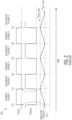
- the timing diagram 200 shows the switch's (S1) gate voltage (Vgate), the switch's (S1) drain voltage (Vdrain), the inductor current (I L1 ), a set of switching cycles 1, 2, 3.
- Each of the switching cycles include a primary stroke time window (i.e. I L1 from 110 to t13 when switch (S1) is “on” and thus L1 charging) and a secondary stroke time window (i.e. I L1 from t13 to t20 when switch (S) "off” and thus L1 discharging).
- the switch (S1) is switched on (i.e. the primary stroke time window) via the gate signal (Vgate) from the controller (IC1) thereby starting the switching cycle (1).
- the inductor current (I L1 ) drops again to the low value (I low_level ), leading to the next switching cycle (2).
- the controller (IC1) determines the high value (I high_level ) and the low value (I low_level ) of the current by sensing a voltage (V) across sense resistor (R1) using the controller's input pins sns1 and sns2 (see Figure 1 ).
- V(R1) V(sns1) - V(sns2).
- Two input pins are required and their input voltages are between ground voltage (GND) and the input voltage (Vin).
- the two input voltages are high voltages (e.g. 400V, 800V, etc.) and require that the controller (IC1) be designed for high voltage operation, which can be expensive.
- the inductor current (I L1 ) is controlled using a continuous conduction mode (CCM), since the inductor current (I L1 ) is always larger than zero (i.e. the current flow is continuous).
- CCM continuous conduction mode
- DCM discontinuous conduction mode
- CCM SMPS circuits where the inductor current (I L1 ) information need not be continuously available.
- the inductor current (I L1 ) is measured only during part of the SMPS's switching cycle.
- Such CCM SMPS circuits are simpler, sensing of the current over the sense resistor (R1) is at low voltage, and the sensing is referred to ground and only one sense input is needed on the controller (IC1).
- FIG 3 represents a first example of a modified SMPS 300.
- the modified SMPS 300 includes an input voltage (Vin), an output voltage (Vout) to be coupled to a load (not shown), a output capacitor (Cout) 302 configured to carry an inductor current 304, a charging circuit 305, an inductor (L1), a diode (D1), and a switching circuit 306.
- the switching circuit 306 includes a current sensing element 308 (e.g. sense resistor (R1)), a switch (S1), and a controller (IC1). Ground (GND) is also shown.
- the output capacitor (Cout) 302 is itself the objective load and the capacitor 302.
- the modified SMPS 300 uses the output capacitor (Cout) 302 as a load.
- the switching circuit 306 is configured to supply an increasing charging current 304 to the capacitor 302 during a primary stroke time window and a decreasing charging current 304 during a secondary stroke time window using the switch (S1).
- the current sensing element 308 e.g. sense resistor (R1)
- R1 sense resistor
- the controller's (IC1) current sense input (Vsns) is now a single pin with a sense voltage with respect to the (GND) pin of the controller.
- the current sensing element 308 e.g. sense resistor (R1)
- the inductor current 304 information is only available during the primary stroke time window when the switch (S1) is closed/conductive.
- an on-time of the modified SMPS 300 may vary from 0.1% to 99.9% depending on the input voltage (Vin) and the capacitor voltage (Vout), there still needs to be a way to constantly adjust a length of the secondary stroke time window so as to properly charge the output capacitor (Cout) 302 with a current between the high value (I high_level ) and the low value (I low_level ).
- Such a way is now discussed below.
- the current sensing element 308 e.g. sense resistor (R1)
- R1 sense resistor
- the controller (IC1) automatically turns the switch (S 1) on which enables the controller (IC1) to again have visibility as to the inductor current 304 (I L1 ) using the current sensing element 308 (e.g. sense resistor (R1)).
- the I low detection window begins (i.e. 110 to t12, t20 to t21, t30 to t32, etc.) as shown and the controller determines the inductor current 304.
- the controller (IC1) shortens the secondary stroke time window (Toff) so as to begin a next primary stroke sooner. However, if the inductor current 304 is at or above (e.g. at 112 or t32) the low current level (I low_level ) then the controller (IC1) lengthens the secondary stroke time window (Toff) so as to begin a next primary stroke later.
- the Toff timer duration is shortened.
- the low current level is exceeded, so for the secondary stroke 1, Toff 1 is increased by making the Toff timer duration longer.
- the Toff2 time is decreased by making the Toff timer duration shorter.
- the low level current will be controlled around the I low_level , (just above or just below) resulting in a continuous current mode (CCM) operation through the inductor (L1) even though the switch (S1) is blocked during the secondary stroke time window.
- CCM continuous current mode
- the switching circuit 306 is configured to end the primary stroke time window (i.e. for the first switching cycle) when the inductor current reaches a first limit (e.g. I high_level ) which the current sensing element 308 (e.g. sense resistor (R1)) can measure/monitor since the switch (S1) is closed.
- a first limit e.g. I high_level
- the current sensing element 308 e.g. sense resistor (R1)
- the controller (ICI) is configured to set the secondary stroke time window to a predicted (e.g. estimated) duration wherein the inductor current decreases until the I low_level current.
- the controller (IC1) is configured to automatically re-start the primary stroke time window (i.e. second switching cycle) and measure the inductor current 304 after the predicted Toff duration using the current sensing element 308 (e.g. sense resistor (R1)) since the switch (S1) is now closed again.
- the current sensing element 308 e.g. sense resistor (R1)
- the controller is configured to shorten the predicted duration so that next primary stroke with increase of the inductor current can begin sooner.
- the charging circuit 305 is configured to lengthen the predicted duration wherein the inductor current decreases until the I low_level current.
- Figure 5 represents an example of a controller 500 for the first example of the modified SMPS 300.
- the low (I low_level ) and high (I high_level ) currents are sensed by comparators Comp1 and Comp2.
- set reset flip flop SR1 is reset, turning off the gate signal.
- set reset flip flop SR1 is set, turning on the Vgate signal. This starts a timer, Timer 1, which creates the I low detection window t10 to t12. If before the end of the I low detection window the Ilow signal becomes high, the output of D-flipflop DFF1 is set and the Toff timer level is adjusted to a higher value in Register1.
- the timers and register can be implemented by analog or digital circuits.
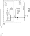
- FIG 6 represents a second example 600 of the modified SMPS.
- the capacitor voltage Vout is now referred with respect to the ground (GND) instead of Vin, however, the inductor current 304 monitoring and control is the same as in Figure 4 .
- the controller's ground (ICgnd) is not the modified SMPS's ground (GND) anymore.
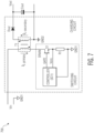
- Figure 7 represents a third example 700 of the modified SMPS.
- the modified SMPS now includes an isolated output by using two coupled inductors (e.g. a transformer with isolated windings).
- the two coupled inductors are for "galvanic isolation”.
- Figure 8 represents an operational timing diagram 800 for the third example 700 of the modified SMPS.
- the transformer's primary (I L-primary ) and secondary (I L-secondary ) current waveforms are shown.
- the third example 700 of the modified SMPS is also considered to be a continuous conduction mode (CCM) SMPS since a sum of the primary and secondary inductor currents is continuous, but not zero.
- CCM continuous conduction mode
- FIG. 9 represents an addition 900 to the first example of the modified SMPS.
- capacitance Cp is added to or is drawn in the circuit diagram.
- Capacitance Cp can be either a bulk capacitance added for EMI reduction, or a parasitic capacitance present in the modified SMPS.
- Figure 10 represents a more detailed operational timing diagram 1000 for the addition 900 to the first example of the modified SMPS.
- the modified SMPS discharges the Cp capacitance, creating a voltage spike on across the current sensing element 308 (e.g. sense resistor (R1)) and is registered by the controller's (IC1) sense voltage (Vsns). The spike is drawn in time window t0 to t10.
- the current sensing element 308 e.g. sense resistor (R1)
- IC1 controller's
- Vsns sense voltage
- the high current and low current comparator outputs are also blanked during the leading edge blanking time to prevent the controller (IC1) from being triggered as well.
- these instructions/steps are implemented as functional and software instructions.
- the instructions can be implemented either using logic gates, application specific chips, firmware, as well as other hardware forms.
- the instructions are embodied as a set of executable instructions in a non-transitory computer-readable or computer-usable media which are effected on a computer or machine programmed with and controlled by said executable instructions.
- Said instructions are loaded for execution on a processor (such as one or more CPUs).
- Said processor includes microprocessors, microcontrollers, processor modules or subsystems (including one or more microprocessors or microcontrollers), or other control or computing devices.
- a processor can refer to a single component or to plural components.
- Said computer-readable or computer-usable storage medium or media is (are) considered to be part of an article (or article of manufacture).
- An article or article of manufacture can refer to any manufactured single component or multiple components.
- the non-transitory machine or computer-usable media or mediums as defined herein excludes signals, but such media or mediums may be capable of receiving and processing information from signals and/or other transitory mediums.
Landscapes
- Engineering & Computer Science (AREA)
- Power Engineering (AREA)
- Dc-Dc Converters (AREA)
Abstract
One example discloses a switched mode power supply (SMPS), comprising: an inductor configured to supply an inductor current to a load; a charging circuit configured to increase an inductor current during a primary stroke time window, and to decrease the inductor current during a secondary stroke time window; wherein the charging circuit is configured to end the primary stroke when the inductor current reaches a high current limit; wherein the charging circuit is configured to set the secondary stroke time window to a predicted duration; wherein the charging circuit is configured to automatically start the primary stroke after the predicted duration and measure the inductor current at the end of a detection window; wherein if the inductor current is below a low limit at the end of the detection window, then the charging circuit is configured to shorten the predicted duration; and wherein if the inductor current is above the low limit at the end of the detection window, then the charging circuit is configured to lengthen the predicted duration.
Description
- The present specification relates to systems, methods, apparatuses, devices, articles of manufacture and instructions for controlling a switched mode power supply (SMPS).
- According to an example embodiment, a switched mode power supply (SMPS), comprising: an inductor configured to supply an inductor current to a load; a charging circuit configured to increase an inductor current during a primary stroke time window, and to decrease the inductor current during a secondary stroke time window; wherein the charging circuit is configured to end the primary stroke when the inductor current reaches a high current limit; wherein the charging circuit is configured to set the secondary stroke time window to a predicted duration; wherein the charging circuit is configured to automatically start the primary stroke after the predicted duration and measure the inductor current at the end of a detection window; wherein if the inductor current is below a low limit at the end of the detection window, then the charging circuit is configured to shorten the predicted duration; and wherein if the inductor current is above the low limit at the end of the detection window, then the charging circuit is configured to lengthen the predicted duration.
- In another example embodiment, the SMPS is operating in a continuous conduction mode (CCM).
- In another example embodiment, the low current limit can be set between a level close to zero and a level close to the high current limit.
- In another example embodiment, the charging circuit is configured to measure the inductor current during the primary stroke time window; and the charging circuit is configured not to measure the inductor current during the secondary stroke time window.
- In another example embodiment, the charging circuit includes a controller, a current sensing element, an inductor, a diode and a switch.
- In another example embodiment, the controller is configured to measure the inductor current using the current sensing element.
- In another example embodiment, during the primary stroke the switch is configured to both conduct the inductor current and enable the current sensing element to measure the inductor current.
- In another example embodiment, during the secondary stroke the switch does not conduct the inductor current and thus the current sensing element cannot measure the inductor current.
- In another example embodiment, the controller is configured to set the switch to a closed state during the primary stroke, and to set the switch to an open state during the secondary stroke.
- In another example embodiment, the current sensing element is a resistor.
- In another example embodiment, a first end of the resistor is coupled to the switch and a second end of the resistor is coupled to a ground potential.
- In another example embodiment, the controller is configured to derive the inductor current from a voltage across the resistor.
- In another example embodiment, the load is a capacitor charged by the inductor current from the charging circuit.
- In another example embodiment, a first end of the capacitor is coupled to the inductor and a second end of the capacitor is coupled to the diode.
- In another example embodiment, further comprising a transformer with isolated windings with the primary winding coupled to the switch and the secondary winding coupled to the diode and to the capacitor.
- The above discussion is not intended to represent every example embodiment or every implementation within the scope of the current or future Claim sets. The Figures and Detailed Description that follow also exemplify various example embodiments.
- Various example embodiments may be more completely understood in consideration of the following Detailed Description in connection with the accompanying Drawings.
-
-
Figure 1 represents a prior art switched mode power supply (SMPS). -
Figure 2 represents a prior art operational timing diagram for the prior art SMPS. -
Figure 3 represents a first example of a modified SMPS. -
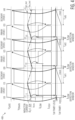
Figure 4 represents an operational timing diagram for the first example of the modified SMPS. -
Figure 5 represents an example of a controller for the first example of the modified SMPS. -
Figure 6 represents a second example of the modified SMPS. -
Figure 7 represents a third example of the modified SMPS. -
Figure 8 represents an operational timing diagram for the third example of the modified SMPS. -
Figure 9 represents an addition to the first example of the modified SMPS. -
Figure 10 represents a more detailed operational timing diagram for the addition to the first example of the modified SMPS. - While the disclosure is amenable to various modifications and alternative forms, specifics thereof have been shown by way of example in the drawings and will be described in detail. It should be understood, however, that other embodiments, beyond the particular embodiments described, are possible as well. All modifications, equivalents, and alternative embodiments falling within the spirit and scope of the appended claims are covered as well.
- Switched mode power supplies (SMPS) have proven to be a more efficient, lighter and smaller form factor circuit for powering a variety of devices, as compared to linear power supplies. SMPSs essentially include a switch (S1) (e.g. MOSFET or other transistor) that continually switches between just two states (i.e. on or off). In some applications, SMPS circuits are used in automotive applications such as for charging the DC-link capacitor of the traction inverter to the high voltage (e.g. 400V, 800V, etc.) of the battery pack.
- In an on-state (i.e. primary-stroke), the SMPS charges a storage device (e.g. an inductor), and in an off-state (i.e. secondary-stroke) the SMPS discharges the storage device by a load. A switching-cycle is defined as one primary-stroke time plus one secondary-stroke time. Further, as herein discussed, charging or discharging of a capacitor results in a change in voltage stored by the capacitor, and an inductor's current change is a result of the inductor magnetizing and demagnetizing. The terms charging and discharging however are often and commonly used for both capacitors and inductors. In this document the "common use" phrasing has been applied for both because both elements are storage devices: the capacitor stores a voltage and the inductor stores a current.
-
Figure 1 represents a prior art switched mode power supply (SMPS) 100. ThisSMPS 100 includes an input voltage (Vin), an output voltage (Vout), an output capacitor (Cout), a sense resistor (R1), an inductor (L1), a switch (S1), a controller (IC1), a diode (D1), and a ground (GND). - The SMPS charges the output capacitor (Cout) by the inductor (L1) current. The switch (S1) in on-state charges the inductor to a peak current. The inductor discharges when the switch (S1) is in off-state and the current flows via diode (D1), also known as a free-wheel diode, in the loop containing the inductor L1, the output capacitor (Cout) and diode (D1). The inductor current (IL1) is regulated by the controller (IC1) based on a measured voltage across sense resistor (R1), (i.e. Vsns = Vsns1 - Vsns2, and IL1 = Vsns/R1).
- The output capacitor's (Cout) current in on-state of the switch (S1) is substantially equal to the inductor current (IL1) flowing through the inductor (L1), the sense resistor (R1) and the switch (S1). The output capacitor's (Cout) current in off-state of the switch (S1) is substantially equal to the inductor current (IL1) flowing through the inductor (L1) and the diode (D1). The output capacitor's (Cout) current can include a current from a load receiving the output voltage (Vout).
-
Figure 2 represents a prior art operational timing diagram 200 for the prior art SMPS 100. The timing diagram 200 shows the switch's (S1) gate voltage (Vgate), the switch's (S1) drain voltage (Vdrain), the inductor current (IL1), a set ofswitching cycles - As soon as the inductor current (IL1) reaches a low value (Ilow_level) at time = 110, the switch (S1) is switched on (i.e. the primary stroke time window) via the gate signal (Vgate) from the controller (IC1) thereby starting the switching cycle (1). The inductor current (IL1) then increases to a high value (Ihigh_level) at time = t13 at which the controller (IC1) turns the switch (S1) off (secondary stroke time window). The inductor current (IL1) drops again to the low value (Ilow_level), leading to the next switching cycle (2).
- The controller (IC1) determines the high value (Ihigh_level) and the low value (Ilow_level) of the current by sensing a voltage (V) across sense resistor (R1) using the controller's input pins sns1 and sns2 (see
Figure 1 ). V(R1) = V(sns1) - V(sns2). Two input pins are required and their input voltages are between ground voltage (GND) and the input voltage (Vin). The two input voltages are high voltages (e.g. 400V, 800V, etc.) and require that the controller (IC1) be designed for high voltage operation, which can be expensive. - The inductor current (IL1) is controlled using a continuous conduction mode (CCM), since the inductor current (IL1) is always larger than zero (i.e. the current flow is continuous). An advantage of CCM over discontinuous conduction mode (DCM) designs is that the average current is larger for the same peak inductor (L1) current and charging of the output capacitor in this automotive application will happen faster. In this design, the inductor current (IL1) information is available continuously.
- Now discussed are CCM SMPS circuits where the inductor current (IL1) information need not be continuously available. In these CCM SMPS circuits, the inductor current (IL1) is measured only during part of the SMPS's switching cycle. Such CCM SMPS circuits are simpler, sensing of the current over the sense resistor (R1) is at low voltage, and the sensing is referred to ground and only one sense input is needed on the controller (IC1).
-
Figure 3 represents a first example of a modifiedSMPS 300. The modifiedSMPS 300 includes an input voltage (Vin), an output voltage (Vout) to be coupled to a load (not shown), a output capacitor (Cout) 302 configured to carry an inductor current 304, a chargingcircuit 305, an inductor (L1), a diode (D1), and aswitching circuit 306. Theswitching circuit 306 includes a current sensing element 308 (e.g. sense resistor (R1)), a switch (S1), and a controller (IC1). Ground (GND) is also shown. Note, in some example embodiments, the output capacitor (Cout) 302 is itself the objective load and thecapacitor 302. - The modified
SMPS 300 uses the output capacitor (Cout) 302 as a load. To charge thecapacitor 302, theswitching circuit 306 is configured to supply an increasing charging current 304 to thecapacitor 302 during a primary stroke time window and a decreasing charging current 304 during a secondary stroke time window using the switch (S1). - Here in
Figure 3 , unlikeFigure 1 , the current sensing element 308 (e.g. sense resistor (R1)) is placed on a low-voltage side in the modifiedSMPS 300 that is between the switch (S1) and the ground (GND). An additional benefit is that the controller's (IC1) current sense input (Vsns) is now a single pin with a sense voltage with respect to the (GND) pin of the controller. - However, in the modified
SMPS 300 the current sensing element 308 (e.g. sense resistor (R1)) is now on a side of the switch (S1) opposite to the output capacitor (Cout) 302, the inductor current 304 information is only available during the primary stroke time window when the switch (S1) is closed/conductive. - Since an on-time of the modified
SMPS 300 may vary from 0.1% to 99.9% depending on the input voltage (Vin) and the capacitor voltage (Vout), there still needs to be a way to constantly adjust a length of the secondary stroke time window so as to properly charge the output capacitor (Cout) 302 with a current between the high value (Ihigh_level) and the low value (Ilow_level). Such a way is now discussed below. -
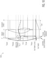
Figure 4 represents an operational timing diagram 400 for the first example of the modifiedSMPS 300. Since the current sensing element 308 (e.g. sense resistor (R1)) is on the low-side of the switch (S1), Vsns can only monitor the inductor current (IL1) between times t = 110 and t = t13, but not between times t = t13 and t = t20. Thus, ending the primary stroke time window can still be done based on direct sensing of the inductor current (IL1), such as discussed inFigure 1 . - However, a duration of the secondary stroke time window now becomes problematic (i.e. when to start the primary stroke time window again), since the controller (IC1) now has no way to directly sense the inductor current (IL1). A solution to this lack of information is now presented that defines the secondary stroke time window using a variable timer (i.e. that controls an off-time (Toff) of the switch (S 1) and an Ilow detection window.
- As shown in
Figure 4 , when the secondary stroke time window ends (i.e. Toff window ends), the controller (IC1) automatically turns the switch (S 1) on which enables the controller (IC1) to again have visibility as to the inductor current 304 (IL1) using the current sensing element 308 (e.g. sense resistor (R1)). At this time, the Ilow detection window begins (i.e. 110 to t12, t20 to t21, t30 to t32, etc.) as shown and the controller determines theinductor current 304. - If the inductor current 304 (IL1) is below (e.g. at t21) the low current level (Ilow_level) then the controller (IC1) shortens the secondary stroke time window (Toff) so as to begin a next primary stroke sooner. However, if the inductor current 304 is at or above (e.g. at 112 or t32) the low current level (Ilow_level) then the controller (IC1) lengthens the secondary stroke time window (Toff) so as to begin a next primary stroke later.
- In other words, if the inductor current 304 (IL1) in the
time window 110 to t12 remains below the Ilow_level, the Toff timer duration is shortened. At time t = t11 (111 is inside the mentioned time window), the low current level is exceeded, so for thesecondary stroke 1,Toff 1 is increased by making the Toff timer duration longer. - For the next primary stroke (primary stroke 2) the Ilow_level current is exceeded at time t = t22. As t22 is outside the t20 to t21 window, for the next secondary stroke (secondary stroke 2), the Toff2 time is decreased by making the Toff timer duration shorter. Thus, by continuously increasing and decreasing a duration of the secondary stroke time window (Toff), the low level current will be controlled around the Ilow_level, (just above or just below) resulting in a continuous current mode (CCM) operation through the inductor (L1) even though the switch (S1) is blocked during the secondary stroke time window.
- Thus the
switching circuit 306 is configured to end the primary stroke time window (i.e. for the first switching cycle) when the inductor current reaches a first limit (e.g. Ihigh_level) which the current sensing element 308 (e.g. sense resistor (R1)) can measure/monitor since the switch (S1) is closed. However, since the switch (S1) is open during the secondary stroke, the controller (ICI) is configured to set the secondary stroke time window to a predicted (e.g. estimated) duration wherein the inductor current decreases until the Ilow_level current. - The controller (IC1) is configured to automatically re-start the primary stroke time window (i.e. second switching cycle) and measure the inductor current 304 after the predicted Toff duration using the current sensing element 308 (e.g. sense resistor (R1)) since the switch (S1) is now closed again.
- As discussed, if the inductor current 304 is below a second limit (e.g. Ilow_level) after the Ilow_detection window, then the controller is configured to shorten the predicted duration so that next primary stroke with increase of the inductor current can begin sooner. However; if the inductor current 304 is above the second limit after the Ilow detection window, then the charging
circuit 305 is configured to lengthen the predicted duration wherein the inductor current decreases until the Ilow_level current. -
Figure 5 represents an example of acontroller 500 for the first example of the modifiedSMPS 300. The low (Ilow_level) and high (Ihigh_level) currents are sensed by comparators Comp1 and Comp2. When the high current (Ihigh_level) level is reached, set reset flip flop SR1 is reset, turning off the gate signal. When the Toff timer elapses, set reset flip flop SR1 is set, turning on the Vgate signal. This starts a timer,Timer 1, which creates the Ilow detection window t10 to t12. If before the end of the Ilow detection window the Ilow signal becomes high, the output of D-flipflop DFF1 is set and the Toff timer level is adjusted to a higher value in Register1. The off timer,Timer 2, starts at t = t13 and when the timer reaches the Toff timer level at t = t20, SR1 is set, starting a next SMPS cycle. The timers and register can be implemented by analog or digital circuits. -
Figure 6 represents a second example 600 of the modified SMPS. Here the capacitor voltage Vout is now referred with respect to the ground (GND) instead of Vin, however, the inductor current 304 monitoring and control is the same as inFigure 4 . Only the controller's ground (ICgnd), is not the modified SMPS's ground (GND) anymore. -
Figure 7 represents a third example 700 of the modified SMPS. Here the modified SMPS now includes an isolated output by using two coupled inductors (e.g. a transformer with isolated windings). As before the inductor current 304 monitoring and control is the same as inFigure 4 . The two coupled inductors are for "galvanic isolation". -
Figure 8 represents an operational timing diagram 800 for the third example 700 of the modified SMPS. The transformer's primary (IL-primary) and secondary (IL-secondary) current waveforms are shown. The third example 700 of the modified SMPS is also considered to be a continuous conduction mode (CCM) SMPS since a sum of the primary and secondary inductor currents is continuous, but not zero. -
Figure 9 represents anaddition 900 to the first example of the modified SMPS. Here capacitance Cp is added to or is drawn in the circuit diagram. Capacitance Cp can be either a bulk capacitance added for EMI reduction, or a parasitic capacitance present in the modified SMPS. -
Figure 10 represents a more detailed operational timing diagram 1000 for theaddition 900 to the first example of the modified SMPS. At the start of the primary stroke time window, the modified SMPS discharges the Cp capacitance, creating a voltage spike on across the current sensing element 308 (e.g. sense resistor (R1)) and is registered by the controller's (IC1) sense voltage (Vsns). The spike is drawn in time window t0 to t10. - To remedy this glitch on Vsns, the controller (IC1) defines a leading edge blanking time (i.e. time window t0 to t10). So while the primary stroke still starts at time t = t0, the Ilow detection window now starts after the leading edge blanking time (time window t0 to t10).
- This blocks Vsns from detecting the spike voltage. The high current and low current comparator outputs are also blanked during the leading edge blanking time to prevent the controller (IC1) from being triggered as well.
- Various instructions and/or operational steps discussed in the above Figures can be executed in any order, unless a specific order is explicitly stated. Also, those skilled in the art will recognize that while some example sets of instructions/steps have been discussed, the material in this specification can be combined in a variety of ways to yield other examples as well, and are to be understood within a context provided by this detailed description.
- In some example embodiments these instructions/steps are implemented as functional and software instructions. In other embodiments, the instructions can be implemented either using logic gates, application specific chips, firmware, as well as other hardware forms.
- When the instructions are embodied as a set of executable instructions in a non-transitory computer-readable or computer-usable media which are effected on a computer or machine programmed with and controlled by said executable instructions. Said instructions are loaded for execution on a processor (such as one or more CPUs). Said processor includes microprocessors, microcontrollers, processor modules or subsystems (including one or more microprocessors or microcontrollers), or other control or computing devices. A processor can refer to a single component or to plural components. Said computer-readable or computer-usable storage medium or media is (are) considered to be part of an article (or article of manufacture). An article or article of manufacture can refer to any manufactured single component or multiple components. The non-transitory machine or computer-usable media or mediums as defined herein excludes signals, but such media or mediums may be capable of receiving and processing information from signals and/or other transitory mediums.
- It will be readily understood that the components of the embodiments as generally described herein and illustrated in the appended figures could be arranged and designed in a wide variety of different configurations. Thus, the detailed description of various embodiments, as represented in the figures, is not intended to limit the scope of the present disclosure, but is merely representative of various embodiments. While the various aspects of the embodiments are presented in drawings, the drawings are not necessarily drawn to scale unless specifically indicated.
- The present invention may be embodied in other specific forms without departing from its spirit or essential characteristics. The described embodiments are to be considered in all respects only as illustrative and not restrictive. The scope of the invention is, therefore, indicated by the appended claims rather than by this detailed description. All changes which come within the meaning and range of equivalency of the claims are to be embraced within their scope.
- Reference throughout this specification to features, advantages, or similar language does not imply that all of the features and advantages that may be realized with the present invention should be or are in any single embodiment of the invention. Rather, language referring to the features and advantages is understood to mean that a specific feature, advantage, or characteristic described in connection with an embodiment is included in at least one embodiment of the present invention. Thus, discussions of the features and advantages, and similar language, throughout this specification may, but do not necessarily, refer to the same embodiment.
- Furthermore, the described features, advantages, and characteristics of the invention may be combined in any suitable manner in one or more embodiments. One skilled in the relevant art will recognize, in light of the description herein, that the invention can be practiced without one or more of the specific features or advantages of a particular embodiment. In other instances, additional features and advantages may be recognized in certain embodiments that may not be present in all embodiments of the invention.
- Reference throughout this specification to "one embodiment," "an embodiment," or similar language means that a particular feature, structure, or characteristic described in connection with the indicated embodiment is included in at least one embodiment of the present invention. Thus, the phrases "in one embodiment," "in an embodiment," and similar language throughout this specification may, but do not necessarily, all refer to the same embodiment.
Claims (15)
- A switched mode power supply, SMPS, comprising:an inductor configured to supply an inductor current to a load;a charging circuit configured to increase an inductor current during a primary stroke time window, and to decrease the inductor current during a secondary stroke time window;wherein the charging circuit is configured to end the primary stroke when the inductor current reaches a high current limit;wherein the charging circuit is configured to set the secondary stroke time window to a predicted duration;wherein the charging circuit is configured to automatically start the primary stroke after the predicted duration and measure the inductor current at the end of a detection window;wherein if the inductor current is below a low limit at the end of the detection window, then the charging circuit is configured to shorten the predicted duration; andwherein if the inductor current is above the low limit at the end of the detection window, then the charging circuit is configured to lengthen the predicted duration.
- The SMPS of claim 1:
wherein the SMPS is operating in a continuous conduction mode, CCM. - The SMPS of claim 1 or 2:
wherein the low current limit can be set between a level close to zero and a level close to the high current limit. - The SMPS of any preceding claim:wherein the charging circuit is configured to measure the inductor current during the primary stroke time window; andwherein the charging circuit is configured not to measure the inductor current during the secondary stroke time window.
- The SMPS of any preceding claim:
wherein the charging circuit includes a controller, a current sensing element, an inductor, a diode and a switch. - The SMPS of claim 5:
wherein the controller is configured to measure the inductor current using the current sensing element. - The SMPS of claim 5 or 6:
wherein during the primary stroke the switch is configured to both conduct the inductor current and enable the current sensing element to measure the inductor current. - The SMPS of any one of claims 5 to 7:
wherein during the secondary stroke the switch does not conduct the inductor current and thus the current sensing element cannot measure the inductor current. - The SMPS of any one of claims 5 to 8:
wherein the controller is configured to set the switch to a closed state during the primary stroke, and to set the switch to an open state during the secondary stroke. - The SMPS of any one of claims 5 to 9:
wherein the current sensing element is a resistor. - The SMPS of claim 10:
wherein a first end of the resistor is coupled to the switch and a second end of the resistor is coupled to a ground potential. - The SMPS of claim 10 or 11:
wherein the controller is configured to derive the inductor current from a voltage across the resistor. - The SMPS of any one of claims 5 to 12:
wherein the load is a capacitor charged by the inductor current from the charging circuit. - The SMPS of claim 13:
wherein a first end of the capacitor is coupled to the inductor and a second end of the capacitor is coupled to the diode. - The SMPS of any one of claims 5 to 14:
further comprising a transformer with isolated windings with the primary winding coupled to the switch and the secondary winding coupled to the diode and to the capacitor.
Applications Claiming Priority (1)
| Application Number | Priority Date | Filing Date | Title |
|---|---|---|---|
| US18/171,214 US20240283364A1 (en) | 2023-02-17 | 2023-02-17 | Switched mode power supply (smps) |
Publications (1)
| Publication Number | Publication Date |
|---|---|
| EP4418512A1 true EP4418512A1 (en) | 2024-08-21 |
Family
ID=89901193
Family Applications (1)
| Application Number | Title | Priority Date | Filing Date |
|---|---|---|---|
| EP24157051.4A Pending EP4418512A1 (en) | 2023-02-17 | 2024-02-12 | Switched mode power supply (smps) |
Country Status (3)
| Country | Link |
|---|---|
| US (1) | US20240283364A1 (en) |
| EP (1) | EP4418512A1 (en) |
| CN (1) | CN118523615A (en) |
Citations (2)
| Publication number | Priority date | Publication date | Assignee | Title |
|---|---|---|---|---|
| CN108390559A (en) * | 2018-05-08 | 2018-08-10 | 杰华特微电子(张家港)有限公司 | Switching power source control circuit based on continuous conduction mode and control method |
| CN208401738U (en) * | 2018-05-08 | 2019-01-18 | 杰华特微电子(张家港)有限公司 | Switching power source control circuit based on continuous conduction mode |
-
2023
- 2023-02-17 US US18/171,214 patent/US20240283364A1/en active Pending
-
2024
- 2024-02-12 EP EP24157051.4A patent/EP4418512A1/en active Pending
- 2024-02-18 CN CN202410183279.5A patent/CN118523615A/en active Pending
Patent Citations (2)
| Publication number | Priority date | Publication date | Assignee | Title |
|---|---|---|---|---|
| CN108390559A (en) * | 2018-05-08 | 2018-08-10 | 杰华特微电子(张家港)有限公司 | Switching power source control circuit based on continuous conduction mode and control method |
| CN208401738U (en) * | 2018-05-08 | 2019-01-18 | 杰华特微电子(张家港)有限公司 | Switching power source control circuit based on continuous conduction mode |
Non-Patent Citations (1)
| Title |
|---|
| CHAO-HSUAN LIU ET AL: "SAR-Controlled Adaptive Off-Time Technique Without Sensing Resistor for Achieving High Efficiency and Accuracy LED Lighting System", IEEE TRANSACTIONS ON CIRCUITS AND SYSTEMS I: REGULAR PAPERS, IEEE, US, vol. 57, no. 6, 1 June 2010 (2010-06-01), pages 1384 - 1394, XP011298562, ISSN: 1549-8328 * |
Also Published As
| Publication number | Publication date |
|---|---|
| CN118523615A (en) | 2024-08-20 |
| US20240283364A1 (en) | 2024-08-22 |
Similar Documents
| Publication | Publication Date | Title |
|---|---|---|
| US11848603B2 (en) | Auxiliary power supply apparatus and method for isolated power converters | |
| US10158282B1 (en) | Switching power supply device | |
| JP5652731B2 (en) | Controller for primary side controlled power converter, integrated circuit for power converter, power converter, method for adjusting bias winding voltage of power supply, and integrated circuit controller for power converter | |
| CN106664020B (en) | Shared Bootstrap Capacitors and Methods for Multiphase Buck Converter Circuits | |
| US10139770B2 (en) | Power source device and image forming apparatus | |
| US12476544B2 (en) | Switching converter | |
| JP6338867B2 (en) | Secondary controller for use in a synchronous flyback converter, power converter, and method of controlling a synchronous flyback converter | |
| US9948187B2 (en) | System and method for a switched-mode power supply | |
| CN107408889B (en) | Power converter | |
| TWI523396B (en) | Forward converter and secondary side switch controller | |
| US20230318469A1 (en) | Drive Circuit | |
| US9742289B2 (en) | Integrated circuit and switching power-supply device | |
| US11223284B2 (en) | System and method for determining a primary switching event in an isolated converter | |
| US20190341859A1 (en) | Active clamp flyback converters | |
| CN107834857B (en) | Power supply control device and insulated switching power supply device | |
| CN117155073A (en) | Switching converter and control circuit thereof | |
| CN117155074A (en) | TURBO mode switching converter and control circuit thereof | |
| US10784785B2 (en) | Monitoring SMPS power switch voltage via switch drain source capacitance | |
| US20250088118A1 (en) | Switch mode power converter with adaptive gate voltage regulation for fast turn-off of synchronous rectifier | |
| US20240283364A1 (en) | Switched mode power supply (smps) | |
| US12388373B2 (en) | Switch mode power converter with synchronous rectifier implementing adaptive turn-off voltage | |
| US20250070641A1 (en) | Power conversion circuit and method | |
| US20200083796A1 (en) | Zero current detector | |
| JP2005295627A (en) | Full-wave rectifying and smoothing circuit and switching power supply device | |
| US12525886B2 (en) | Converter circuit |
Legal Events
| Date | Code | Title | Description |
|---|---|---|---|
| PUAI | Public reference made under article 153(3) epc to a published international application that has entered the european phase |
Free format text: ORIGINAL CODE: 0009012 |
|
| STAA | Information on the status of an ep patent application or granted ep patent |
Free format text: STATUS: THE APPLICATION HAS BEEN PUBLISHED |
|
| AK | Designated contracting states |
Kind code of ref document: A1 Designated state(s): AL AT BE BG CH CY CZ DE DK EE ES FI FR GB GR HR HU IE IS IT LI LT LU LV MC ME MK MT NL NO PL PT RO RS SE SI SK SM TR |
|
| STAA | Information on the status of an ep patent application or granted ep patent |
Free format text: STATUS: REQUEST FOR EXAMINATION WAS MADE |
|
| 17P | Request for examination filed |
Effective date: 20250221 |