EP4418468A1 - Flat socket contact device - Google Patents
Flat socket contact device Download PDFInfo
- Publication number
- EP4418468A1 EP4418468A1 EP24157053.0A EP24157053A EP4418468A1 EP 4418468 A1 EP4418468 A1 EP 4418468A1 EP 24157053 A EP24157053 A EP 24157053A EP 4418468 A1 EP4418468 A1 EP 4418468A1
- Authority
- EP
- European Patent Office
- Prior art keywords
- contact
- wall
- flat socket
- contact device
- socket contact
- Prior art date
- Legal status (The legal status is an assumption and is not a legal conclusion. Google has not performed a legal analysis and makes no representation as to the accuracy of the status listed.)
- Pending
Links
Images




Classifications
-
- H—ELECTRICITY
- H01—ELECTRIC ELEMENTS
- H01R—ELECTRICALLY-CONDUCTIVE CONNECTIONS; STRUCTURAL ASSOCIATIONS OF A PLURALITY OF MUTUALLY-INSULATED ELECTRICAL CONNECTING ELEMENTS; COUPLING DEVICES; CURRENT COLLECTORS
- H01R13/00—Details of coupling devices of the kinds covered by groups H01R12/70 or H01R24/00 - H01R33/00
- H01R13/46—Bases; Cases
- H01R13/533—Bases, cases made for use in extreme conditions, e.g. high temperature, radiation, vibration, corrosive environment, pressure
-
- H—ELECTRICITY
- H01—ELECTRIC ELEMENTS
- H01R—ELECTRICALLY-CONDUCTIVE CONNECTIONS; STRUCTURAL ASSOCIATIONS OF A PLURALITY OF MUTUALLY-INSULATED ELECTRICAL CONNECTING ELEMENTS; COUPLING DEVICES; CURRENT COLLECTORS
- H01R13/00—Details of coupling devices of the kinds covered by groups H01R12/70 or H01R24/00 - H01R33/00
- H01R13/02—Contact members
-
- H—ELECTRICITY
- H01—ELECTRIC ELEMENTS
- H01R—ELECTRICALLY-CONDUCTIVE CONNECTIONS; STRUCTURAL ASSOCIATIONS OF A PLURALITY OF MUTUALLY-INSULATED ELECTRICAL CONNECTING ELEMENTS; COUPLING DEVICES; CURRENT COLLECTORS
- H01R13/00—Details of coupling devices of the kinds covered by groups H01R12/70 or H01R24/00 - H01R33/00
- H01R13/02—Contact members
- H01R13/10—Sockets for co-operation with pins or blades
- H01R13/11—Resilient sockets
- H01R13/113—Resilient sockets co-operating with pins or blades having a rectangular transverse section
-
- H—ELECTRICITY
- H01—ELECTRIC ELEMENTS
- H01R—ELECTRICALLY-CONDUCTIVE CONNECTIONS; STRUCTURAL ASSOCIATIONS OF A PLURALITY OF MUTUALLY-INSULATED ELECTRICAL CONNECTING ELEMENTS; COUPLING DEVICES; CURRENT COLLECTORS
- H01R13/00—Details of coupling devices of the kinds covered by groups H01R12/70 or H01R24/00 - H01R33/00
- H01R13/02—Contact members
- H01R13/10—Sockets for co-operation with pins or blades
- H01R13/11—Resilient sockets
-
- H—ELECTRICITY
- H01—ELECTRIC ELEMENTS
- H01R—ELECTRICALLY-CONDUCTIVE CONNECTIONS; STRUCTURAL ASSOCIATIONS OF A PLURALITY OF MUTUALLY-INSULATED ELECTRICAL CONNECTING ELEMENTS; COUPLING DEVICES; CURRENT COLLECTORS
- H01R13/00—Details of coupling devices of the kinds covered by groups H01R12/70 or H01R24/00 - H01R33/00
- H01R13/02—Contact members
- H01R13/15—Pins, blades or sockets having separate spring member for producing or increasing contact pressure
- H01R13/187—Pins, blades or sockets having separate spring member for producing or increasing contact pressure with spring member in the socket
-
- H—ELECTRICITY
- H01—ELECTRIC ELEMENTS
- H01R—ELECTRICALLY-CONDUCTIVE CONNECTIONS; STRUCTURAL ASSOCIATIONS OF A PLURALITY OF MUTUALLY-INSULATED ELECTRICAL CONNECTING ELEMENTS; COUPLING DEVICES; CURRENT COLLECTORS
- H01R13/00—Details of coupling devices of the kinds covered by groups H01R12/70 or H01R24/00 - H01R33/00
- H01R13/02—Contact members
- H01R13/193—Means for increasing contact pressure at the end of engagement of coupling part, e.g. zero insertion force or no friction
-
- H—ELECTRICITY
- H01—ELECTRIC ELEMENTS
- H01R—ELECTRICALLY-CONDUCTIVE CONNECTIONS; STRUCTURAL ASSOCIATIONS OF A PLURALITY OF MUTUALLY-INSULATED ELECTRICAL CONNECTING ELEMENTS; COUPLING DEVICES; CURRENT COLLECTORS
- H01R13/00—Details of coupling devices of the kinds covered by groups H01R12/70 or H01R24/00 - H01R33/00
- H01R13/02—Contact members
- H01R13/20—Pins, blades, or sockets shaped, or provided with separate member, to retain co-operating parts together
-
- H—ELECTRICITY
- H01—ELECTRIC ELEMENTS
- H01R—ELECTRICALLY-CONDUCTIVE CONNECTIONS; STRUCTURAL ASSOCIATIONS OF A PLURALITY OF MUTUALLY-INSULATED ELECTRICAL CONNECTING ELEMENTS; COUPLING DEVICES; CURRENT COLLECTORS
- H01R13/00—Details of coupling devices of the kinds covered by groups H01R12/70 or H01R24/00 - H01R33/00
- H01R13/40—Securing contact members in or to a base or case; Insulating of contact members
-
- H—ELECTRICITY
- H01—ELECTRIC ELEMENTS
- H01R—ELECTRICALLY-CONDUCTIVE CONNECTIONS; STRUCTURAL ASSOCIATIONS OF A PLURALITY OF MUTUALLY-INSULATED ELECTRICAL CONNECTING ELEMENTS; COUPLING DEVICES; CURRENT COLLECTORS
- H01R13/00—Details of coupling devices of the kinds covered by groups H01R12/70 or H01R24/00 - H01R33/00
- H01R13/46—Bases; Cases
- H01R13/502—Bases; Cases composed of different pieces
-
- H—ELECTRICITY
- H01—ELECTRIC ELEMENTS
- H01R—ELECTRICALLY-CONDUCTIVE CONNECTIONS; STRUCTURAL ASSOCIATIONS OF A PLURALITY OF MUTUALLY-INSULATED ELECTRICAL CONNECTING ELEMENTS; COUPLING DEVICES; CURRENT COLLECTORS
- H01R13/00—Details of coupling devices of the kinds covered by groups H01R12/70 or H01R24/00 - H01R33/00
- H01R13/62—Means for facilitating engagement or disengagement of coupling parts or for holding them in engagement
- H01R13/639—Additional means for holding or locking coupling parts together, after engagement, e.g. separate keylock, retainer strap
-
- H—ELECTRICITY
- H01—ELECTRIC ELEMENTS
- H01R—ELECTRICALLY-CONDUCTIVE CONNECTIONS; STRUCTURAL ASSOCIATIONS OF A PLURALITY OF MUTUALLY-INSULATED ELECTRICAL CONNECTING ELEMENTS; COUPLING DEVICES; CURRENT COLLECTORS
- H01R11/00—Individual connecting elements providing two or more spaced connecting locations for conductive members which are, or may be, thereby interconnected, e.g. end pieces for wires or cables supported by the wire or cable and having means for facilitating electrical connection to some other wire, terminal, or conductive member, blocks of binding posts
- H01R11/03—Individual connecting elements providing two or more spaced connecting locations for conductive members which are, or may be, thereby interconnected, e.g. end pieces for wires or cables supported by the wire or cable and having means for facilitating electrical connection to some other wire, terminal, or conductive member, blocks of binding posts characterised by the relationship between the connecting locations
- H01R11/05—Individual connecting elements providing two or more spaced connecting locations for conductive members which are, or may be, thereby interconnected, e.g. end pieces for wires or cables supported by the wire or cable and having means for facilitating electrical connection to some other wire, terminal, or conductive member, blocks of binding posts characterised by the relationship between the connecting locations the connecting locations having different types of direct connections
-
- H—ELECTRICITY
- H01—ELECTRIC ELEMENTS
- H01R—ELECTRICALLY-CONDUCTIVE CONNECTIONS; STRUCTURAL ASSOCIATIONS OF A PLURALITY OF MUTUALLY-INSULATED ELECTRICAL CONNECTING ELEMENTS; COUPLING DEVICES; CURRENT COLLECTORS
- H01R13/00—Details of coupling devices of the kinds covered by groups H01R12/70 or H01R24/00 - H01R33/00
- H01R13/02—Contact members
- H01R13/15—Pins, blades or sockets having separate spring member for producing or increasing contact pressure
-
- H—ELECTRICITY
- H01—ELECTRIC ELEMENTS
- H01R—ELECTRICALLY-CONDUCTIVE CONNECTIONS; STRUCTURAL ASSOCIATIONS OF A PLURALITY OF MUTUALLY-INSULATED ELECTRICAL CONNECTING ELEMENTS; COUPLING DEVICES; CURRENT COLLECTORS
- H01R13/00—Details of coupling devices of the kinds covered by groups H01R12/70 or H01R24/00 - H01R33/00
- H01R13/62—Means for facilitating engagement or disengagement of coupling parts or for holding them in engagement
-
- H—ELECTRICITY
- H01—ELECTRIC ELEMENTS
- H01R—ELECTRICALLY-CONDUCTIVE CONNECTIONS; STRUCTURAL ASSOCIATIONS OF A PLURALITY OF MUTUALLY-INSULATED ELECTRICAL CONNECTING ELEMENTS; COUPLING DEVICES; CURRENT COLLECTORS
- H01R2201/00—Connectors or connections adapted for particular applications
- H01R2201/26—Connectors or connections adapted for particular applications for vehicles
Definitions
- the invention relates to a flat socket contact device, in particular for use in automotive engineering.
- the flat socket contact device according to the invention can be used in particular for an electrical battery module in vehicle that can be electrically powered.
- the flat socket contact device according to the invention is suitable for use in the high-current range.
- the problem addressed by the invention lies in providing an improved flat socket contact device for an electrical high-current connection.
- an electrical flat socket contact device for an electrical power connection comprising:
- the flat socket contact device comprises a carrier structure which forms a primarily cuboid contact box unit into which a primarily cuboid tab contact can be plugged to create the high-current connection.
- a primarily cuboid contact body for contacting the tab contact is arranged in the contact box unit.
- the contact body On a top wall, the contact body, there is arranged at least one spring element unit, by means of which the contacting of the plugged tab contact can be effected.
- the top wall of the carrier structure has a greater wall thickness here than the base wall of the carrier structure.
- the restoring forces of the spring element unit can be used to generate contact normal forces in the region of 60 newtons.
- spring element units with higher restoring forces can also be used, which enable higher contact normal forces if this is required.
- the high contact normal forces exerted by the spring element unit on the tab contact can be used to press the tab contact more firmly against the contact body. This enables an efficient electrical connection to be made between the self-plugged tab contact and the contact body, which is suitable for a high-current connection.
- the high contact normal forces that can be provided by the spring element unit also ensure greater vibration resistance of the electrical connection between the tab contact and the contact body.
- the base wall and the top wall are formed by the two largest surfaces of the cuboid carrier structure or the contact box unit and are arranged opposite each other.
- the carrier structure or contact box unit defines a primarily cuboid receiving space.
- the top wall comprises an inner partial wall and an outer partial wall, wherein the inner and outer partial walls are arranged to contact one another in a planar manner, wherein the inner partial wall defines an inner wall of the contact box unit, and wherein the at least one spring element unit is formed on the inner partial wall.
- the technical advantage of this is that the top wall can be generated with twice the wall thickness using two partial walls arranged in planar contact with each other.
- the inner partial wall which defines an inner wall of the contact box unit, comprises the spring element unit that extends into the interior of the contact box unit.
- the outer partial wall resting on the inner partial wall does not comprise a spring element unit and is primarily used to stiffen the inner partial wall in order to enable the contact normal force of the spring element unit to be increased.
- the outer partial wall resting on the inner partial wall thus enables a technically simple stiffening of the entire carrier structure and thus an increase in the possible contact normal force of the spring element unit, which can exert an increased contact normal force on the tab contact and thus enables improved electrical contacting of the inserted tab contact.
- the wall thickness of the top wall can be at least twice the wall thickness of the base wall.
- the base wall is integrally connected to the inner partial wall via a first side wall element and via a second side wall element, wherein the first and second wall elements define side walls of the contact box unit.
- a robust carrier structure can be provided by the integral connection of the base wall to the inner partial wall via a first side wall element and to the outer partial wall via a second side wall element, each of which defines side walls of the contact box unit.
- the two side wall elements delimit the primarily cuboid receiving space of the contact box unit.
- the carrier structure is designed as a multi-surface bending structure.
- the first and second side wall elements are each arranged at an angle to the base wall and to the inner and outer partial walls via 90° bends.
- the 90° bends of the first and second side wall elements relative to the base wall and the inner and outer partial walls enable a simple and robust design of the carrier structure.
- the 90° bends describe, in accordance with the invention, an angular range between 75° and 105°, preferably between 80° and 100°, even more preferably between 85° and 95°, and particularly preferably 90°.
- the at least one spring element unit is formed integrally on the inner partial wall.
- the at least one spring element unit is designed as a bending element and is arranged on a side edge of the inner partial wall, wherein the spring element unit extends at least partially along the inner partial wall over a 180° bend.
- the design of the spring element unit as a bending element, which is formed integrally on the inner partial wall, enables a robust spring element unit.
- the spring element unit is easy to manufacture within the contact box unit thanks to the 180° bend, which allows the spring element unit to be aligned partially parallel to the inner partial wall.
- the 180° bends describe, in accordance with the invention, an angular range between 165° and 195°, preferably between 170° and 190°, even more preferably between 175° and 185°, and particularly preferably 180°.
- the inner partial wall and the outer partial wall are connected to each other via at least one clinch connection and/or a welded connection.
- the technical advantage of this is that the clinch connection and/or the welded connection enable the inner and outer partial walls to be securely and robustly fixed together.
- a fixing catch is arranged on the outer partial wall and/or on the base wall for fixing the flat socket contact device to a holding device.
- the flat socket contact device can be securely arranged on a mounting device, for example in a vehicle, thanks to the fixing catches on the outer partial wall and/or the base wall.
- the fixing catches allow the flat socket contact device to be mounted easily.
- a plurality of contacting domes and/or spring element units are formed on the contact body for contacting the tab contact.
- the contact body is fixed to the base wall of the carrier structure within the contact box unit via at least one clinch connection.
- a clinch connection can also be designed as a locking tab connection.
- the at least one clinch connection is formed at a front end, via which the tab contact can be inserted into the contact box unit, and/or at a rear end of the contact box unit arranged opposite the front end.
- the clinch connection at the front end prevents the contact body from slipping out of the contact box unit via the insertion opening.
- the clinch connections at the rear end of the contact box unit can prevent the contact body from tilting relative to the contact box unit.
- the clinch connections at the rear end are arranged on a side region of the contact body.
- the front end of the contact box unit is defined by the insertion opening of the contact box unit.
- the contact body comprises at least one receiving recess at a front end and/or on a side region of the contact body for receiving the at least one clinch connection.
- the contact box unit is limited at the rear end by a rear wall of the carrier structure.
- the rear wall is formed in one piece on a side edge of the inner partial wall, wherein the rear wall is arranged at an angle to the inner partial wall via a 90° bend.
- the 90° bend of the rear wall relative to the inner partial wall enables a simple technical solution for aligning the rear wall relative to the contact box unit.
- the carrier structure is made of stainless steel or a copper compound.
- the carrier structure is configured via the at least one spring element unit to provide a contact normal force of up to 40 N, preferably 50 N, particularly preferably 60 N, for contacting the inserted tab contact.
- This enables high-performance electrical contacting of the tab contact with the contact body, which enables high-current use in the high-current range.
- the high contact normal forces can be used to improve the vibration resistance of the connection.
- the contact normal force is oriented perpendicular to the surface of the tab contact.
- the tab contact can be clamped in the contact box unit via the spring element unit.
- the flat socket contact device is designed for electrical voltages of at least approximately: 200V, 300V, 400V, 500V, 1kV, 1.25kV or 1.5kV and/or for electrical currents of at least approximately: 200A, 300A, 400A, 500A, 600A, 800A, 1kA or 1.25kV.
- the flat socket contact device can be used for a wide range of electrical voltages and electrical currents, particularly in the high-voltage or high-current range.
- an electrical connection system with an electrical flat socket contact device according to one of the preceding embodiments and a primarily cuboid tab contact is provided.
- Figure 1 shows a schematic representation of an electrical connection system 200 according to one embodiment.
- the electrical connection system 200 shown comprises an electrical flat socket contact device 100 and a primarily cuboid tab contact 105.
- the electrical flat socket contact device 100 comprises a carrier structure 101.
- the carrier structure 101 defines a primarily cuboid contact box unit 103.
- the tab contact 105 can be inserted into the contact box unit 103 along a longitudinal direction L of the carrier structure 101 via an opening 153 of the carrier structure 101.
- the carrier structure 101 comprises a base wall 109, a top wall 111 arranged opposite the base wall 109, and two side wall elements 121, 123 connecting the base wall 109 and the top wall 111 to one another.
- the first and second side wall elements 115, 117 are designed to be spaced apart parallel to one another along the transverse direction Q.
- a primarily cuboid contact body 107 is arranged in the primarily cuboid contact box unit 103.
- the contact body 107 rests on the base wall 109 of the carrier structure.
- the top wall 111 and the base wall 109 are defined by the two large surfaces of the cuboid contact box unit 103 and are arranged parallel to each other and spaced apart along a height direction H of the contact box unit 103.
- the top wall 111 has a greater wall thickness than the base wall 109.
- the wall thickness of the top wall 111 is at least twice as great as the wall thickness of the base wall 109.
- at least one spring element unit 113 is arranged on the top wall 111.
- the spring element unit 113 extends into the contact box unit 103 and serves to make contact with the tab contact 105 inserted into the contact box unit 103. A contact normal force can be exerted, via the spring element unit 113, on the tab contact 105 inserted into the contact box unit 103.
- the tab contact 105 is pressed against the contact body 107 via the contact normal force, as a result of which the electrical contact is made between the tab contact 105 and the contact body 107.
- the spring element unit 113 is connected to the top wall 111, in particular to the inner partial wall 115, via a 180° bend. The 180° bend is formed at the front end 139 on the inner partial wall 115 and the spring element unit 113 thus runs parallel to the longitudinal axis L of the contact box unit 103.
- the contact body 107 is also connected to a line connection element 151 for the electrical current connection.
- the line connection element 151 is arranged outside the contact box unit 103 defined by the carrier structure 101 and is used for the electrical connection.
- the line connection element 151 can, for example, be designed as a cable lug, by means of which the flat socket contact device 100 can be connected to a cable.
- the contact body 107 can be made of a copper alloy, for example.
- the line connection element 151 can be designed as a crimping, ultrasonic or welding pad.
- the inserted tab contact 105 is arranged between the contact body 107 arranged in the contact box unit 103 and the top wall 111 of the carrier structure 101.
- the contact body 107 has a plurality of contacting domes 133 for electrical contacting.
- the contacting domes 133 are formed on a surface 165 of the contact body 107 and protrude from this surface 165 into the contact box unit 103.
- the inserted tab contact 105 is thus pressed onto the contact body 107 via the contact pressure of the spring element unit 113, whereby point contacting of the tab contact 105 with the plurality of contacting domes 133 is effected.
- the contacting domes 133 each comprise a partially cylindrical shape with an at least partially circular outer surface 134 and an at least partially spherical end region 136.
- the contacting domes 133 have at least partially cylindrical shapes and comprise at least partially circular outer surfaces 134, which protrude from the surface 165.
- the surface 165 is formed by one of the two large surfaces of the cuboid contact body 107 and is oriented parallel to the inner partial wall 115.
- the contact body 107 is connected to the carrier structure 101 via clinch connections 137.
- the clinch connections 137 are connected here integrally to the carrier structure 101 and, in the embodiment shown, engage in receiving recesses 145 formed on a side region 143 of the contact body 107.
- the side region 143 is formed by at least one of the small surfaces of the cuboid contact body 107, which rest against the two side wall elements 121, 123.
- the clinch connections 137 are formed in a rear end 141 of the carrier structure 101.
- the rear end 141 is arranged here opposite a front end 139 of the carrier structure 101.
- the top wall 111 comprises an outer partial wall 117 and an inner partial wall, not visible in Figure 1 .
- the inner and outer partial walls 115, 117 are arranged here to lie flat on top of each other.
- the outer partial wall 117 which defines an outer boundary of the carrier structure 101, has a fixing catch 131.
- the fixing catch 131 serves to fix the flat socket contact device 100 in a receiving structure, for example in a vehicle.
- the flat socket contact device 100 can be fixed securely in a corresponding holding structure for holding contact devices via the fixing catch 131.
- the first and second side wall elements 121, 123 each have, at the end face 139, two foldover elements 167 bent in the direction of the receiving chamber 103.
- the foldover elements 167 have a 180° bend and are arranged at least partially parallel to the first and second wall elements 121, 123.
- Figure 2 shows a schematic representation of an electrical flat socket contact device 100 according to one embodiment.
- the embodiment in Figure 2 is based on the embodiment in Figure 1 and comprises a large part of the features described there.
- Figure 2 shows the design of the inner and outer partial walls 115, 117 of the top wall 111.
- the inner and outer partial walls 115, 117 are arranged here to lie flat on top of each other.
- the inner partial wall 115 describes an inner ceiling boundary of the contact box unit 103.
- the already mentioned at least one spring element unit 113 is formed on the inner partial wall 115.
- the spring element unit 113 is designed as a bending element and extends into the receiving space of the contact box unit 103.
- the spring element unit 113 has a 180° bend 169 and is integrally connected to the inner partial wall 115.
- the spring element unit 113 is arranged to extend at least partially along the inner partial wall 115 via the 180° bend 169.
- the spring element unit is arranged here to exert a contact normal force in the direction of the base wall 109 of the carrier structure 101.
- the 180° bend of a side edge of the inner partial wall 115 is formed and thus runs parallel to the second side wall element 123.
- the side edge of the inner partial wall 115 is aligned parallel to the second side wall element 123.
- the spring element unit 113 thus extends perpendicular to the longitudinal axis L of the contact box unit 103.
- the spring element unit 113 which is formed as a bending element 125, comprises a first end 114 and an oppositely arranged second end 116.
- the first end is connected to the 180° bend, while the second end 116 is formed as a free end.
- two bar elements 118, 122 are formed which are connected to each other via a bend 120.
- the two inclined bar elements 118, 122 of the spring element unit 113 are at an angle to each other due to the bend 120.
- the second end 116 is also in contact with the inner partial wall 115.
- the two bar elements 118, 122 and the bend 120 are spaced apart from the inner partial wall 115 and protrude into the receiving space of the contact box unit 103.
- the contact body 107 in addition to the clinch connections 137 formed at the rear end 141, the contact body 107 is additionally fixed to the carrier structure 101 and in particular in the contact box unit 103 via a further clinch connection 137 formed at the front end 139.
- the contact body 107 has a further receiving recess 145 at the front end 139, into which the clinch connection 137 of the carrier structure 101 can engage.
- the clinch connection 137 is connected integrally to the base wall 109 of the carrier structure 101.
- the clinch connection 137 shown also has a curved region 163, which extends from the surface 165 of the contact body 107 into the contact box unit 103.
- the contact body 107 has the aforementioned plurality of contacting domes 133.
- the contacting domes 133 are again primarily cylindrical in shape and protrude from the surface 165 of the contact body 107.
- the contacting domes 133 are formed in groups spaced apart from one another over the surface 165 of the contact body 107.
- the carrier structure 101 also has a rear wall 147 at the rear end 141.
- the rear wall 147 is connected to the base wall 109 and is arranged at an angle to the latter.
- the contact box unit 103 is delimited towards the rear end 141 by the rear wall 147.
- the inner and outer partial walls 115, 117 are furthermore fixed into one another by two clinch connections 129.
- the clinch connections 129 are formed integrally on the outer partial wall 117 at the front end 139 and engage around the inner partial wall 115.
- the first side wall element 121 is largely formed as a continuous wall element.
- the second side wall element 123 is formed by two bar elements 173, which are arranged one at the front end 139 and one at the rear end 141.
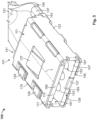
- Figure 3 shows a further schematic representation of an electrical flat socket contact device 100 according to a further embodiment.
- Figure 3 is based on the embodiment in Figure 2 and comprises all the features described there.
- a further fixing catch 131 is formed on the base wall 109 of the carrier structure 101.
- the further fixing catch 131 again enables the flat socket contact device 100 to be fixed to a corresponding receptacle.
- the fixing catches 131 on the base wall 109 and on the outer partial wall 117 are each formed by a punching and bending process from the respective walls 109, 117 and protrude from these.
- Figure 4 shows a further schematic representation of an electrical flat socket contact device 100 according to a further embodiment.
- the inner and outer partial walls 115, 117 are fixed together by two further clinch connections 129 in addition to the clinch connections 129 formed at the front end 139.
- the further clinch connections 129 are formed here on a side region 175 of the carrier structure 101.
- the clinch connections 129 are formed integrally on the first side wall element 121.
- the outer partial wall 117 has two receiving recesses 177 for receiving the side clinch connections 129, said recesses being arranged on the side region 175 of the outer partial wall 117.
- Figure 5 shows a further schematic representation of an electrical flat socket contact device 100 according to a further embodiment.
- the embodiment shown in Figure 5 is based on the embodiment in Figure 4 and comprises all the features described there.
- the embodiment shown differs from the embodiment in Figure 4 in that the second side wall element 123 is designed as a continuous wall element and is not formed by the two bar elements 173 as in the embodiment in Figure 4 .
- the clinch connection 137 formed at the front end 139 for fixing the contact body 107 is formed without the curved region 163.
- the clinch connection 137 is flush with the surface 165 of the contact body 107.
- first and second side wall elements 121, 123 have the side foldover elements 167 already shown in Figure 1 .
- the outer partial wall 117 has no clinch connections 129 at the front end 139.
- the inner and outer partial walls 115, 117 are thus fixed to one another exclusively via the clinch connections 129 formed on the side region 175.
- Figure 6 shows a further schematic representation of an electrical flat socket contact device 100 according to a further embodiment.
- the embodiment in Figure 6 is based on the embodiment in Figure 4 .
- no further clinch connections 129 are formed on the side region 175.
- the clinch connection 137 formed at the front end 139 does not have a curved region 163.
- the clinch connection 137 has a contact region 179 that rests directly on the surface 165 of the contact body 107.
- the contacting domes 133 of the contact body 107 are replaced by contacting springs 135.
- the contacting springs 135 run perpendicular to the longitudinal direction L of the carrier structure 101.
- the longitudinal direction L runs here from the front end 139 to the rear end 141.
- the plurality of contacting springs 135 are separated by slotted recesses 159, which are also arranged perpendicular to the longitudinal direction L.
- the contacting springs 135 each have a first end 181 and an oppositely arranged second end 183.
- the first end 181 is formed integrally on the contact body 107, while the second end 183 is formed as a free end.
- the contacting springs 135 also have a curved region 185.
- the curved region 185 extends between the first and second ends 181, 183 and extends into the receiving space of the contact box unit 103.
- the second ends 183 of the contacting springs 135 are freely mounted in round recesses 161, so that the second end 183 is freely movable relative to the contact body 107 and the contacting springs are set up to provide a contact normal force via the curved region 183.
- Figure 7 shows a further schematic representation of an electrical flat socket contact device 100 according to a further embodiment.
- Figure 7 primarily shows a side view of the flat socket contact device 100 in Figure 6 .
- the contacting springs 135 are shown aligned parallel to each other and perpendicular to the longitudinal direction L.
- the contacting springs 135 are separated from each other by the slotted recesses 177 and the second ends 183 are freely movable in the round recesses 161.
- Figure 8 shows a further schematic representation of an electrical flat socket contact device 100 according to a further embodiment.
- the carrier structure 101 of the flat socket contact device 100 is designed as a coherent bending structure.
- the individual components of the carrier structure 101 i.e. the base wall 109, the inner and outer partial walls 115, 117, and the first and second side wall elements 121, 123 are integrally connected to one another in the embodiment shown.
- the base wall 109 is connected here to the first side wall element 121 at a third side edge 187 and to the second side wall element 123 via a fourth side edge 189.
- the outer partial wall 117 is also connected to the second side wall element 123 via a fifth side edge 191.
- the inner partial wall 115 is connected to the first side wall element 121 via a second side edge 149.
- the spring element unit 113 is formed on a first side edge 127 of the inner partial wall 115.
- the first and second side wall elements 121, 123 have 90° bends 171.
- the carrier structure 101 is shown in an unbent form and describes a flat structure.
- the three-dimensional, primarily cuboid carrier structure 101 of Figures 1 to 7 is produced by corresponding bending processes at the 90° bends 171 and 180° bends 169.
- the outer partial wall 117 has the two clinch connections 129 spaced apart from one another at a front edge 193. Similarly, the outer partial wall 117 has two clinch connections 129 at the rear edge 195.
- the base plate 109 has a further clinch connection 137 at a front edge 193 and two laterally arranged clinch connections 137 at a rear edge 195.
- the clinch connections 129, 137 each have 180° bends 169, by means of which the clinch connections 129 can be bent around the inner partial wall 115 and the clinch connections 137 can be bent around the contact body 107.
- the inner partial plate 115 also has the rear wall 147 at a rear edge 195.
- the rear wall 147 is in turn arranged on the inner partial plate 115 via a 90° bend 171 and can thus be bent through 90° in order to provide the rearward delimitation of the contact box unit 103.
- the contacting spring 135 is arranged on the first side edge 127 via the 180° bend 169.
- the spring element unit is designed as a bending element 125 and has three spring element units 113 arranged next to one another, which are each separated from one another by slots 155.
- the bending element 125 has a first end 114 and an oppositely arranged second end 116.
- the bending element 125 is connected to the 180° bend 169 via the first end 114, while the second end 116 is formed as a free end.
- the individual spring element units 113 have two bar elements 118, 122, which are connected to one another via a bend 120.
- the bar elements 118, 122 can be arranged at an angle to one another via the bend 120.
- the spring element units 113 are able to effect a corresponding contact normal force.
- the 180° bend 169 allows the spring element units 113 or the bending element 125 to be arranged at least partially parallel to the inner partial wall 115, since the spring element units 113 are arranged perpendicular to the longitudinal direction L of the contact box unit and extend along the inner partial wall 115, as shown in the embodiments of Figures 2 to 4 and 6 and 7 .
- the second ends 116 can make contact here with the inner partial wall 115, while the bar elements 118, 122 connected to one another by the bend 120 are spaced apart from the inner partial wall 115 and extend into the receiving space of the contact box unit 103, in order to ensure the return
- the spring element units 113 or the spring element units 113 of the bending element 125 can also be formed at the front edge 193 of the inner partial wall 115 via a corresponding 180° bend 169, as shown in the embodiments of Figures 1 and 5 .
- the spring element units 113 of the bending element 125 run parallel to the longitudinal axis L of the contact box unit 103.
- the first side wall element 121 has four slots 155, which are arranged in the region of the 90° bends 171.
- the second side wall element 123 has a recess 157 and is primarily formed by the bar elements 173.
- the base wall 109 and the outer partial wall 117 have the fixing catches 131.
- the fixing catches 131 each have a first end 196 and an opposite second end 197.
- the first end 196 is connected to the base wall 109 or the outer partial wall 117 via a bend 198.
- the second end 197 is formed as a free end.
- the fixing catch 131 can be bent relative to the base wall 109 or the outer partial wall 117 at an angle that can be set as desired. This allows the fixing catch 137 to generate a contact normal force.
- the fixing catch 137 is manufactured by a stamping process and is surrounded by a primarily U-shaped slot 199.
- the carrier structure 101 is made of stainless steel.
- the carrier structure 101 can be manufactured from a corresponding sheet material by a stamping process and transformed into the three-dimensional carrier structure 101 of Figures 1 to 7 by the bending processes described above at the bends 169, 171, 198 provided for this purpose.
- the embodiment shown in Figure 8 is primarily merely exemplary and may deviate from the embodiment shown in respect of various factors.
- the spring element units 113 may differ in shape, number and orientation from the embodiment shown.
Landscapes
- Connecting Device With Holders (AREA)
- Coupling Device And Connection With Printed Circuit (AREA)
Abstract
The invention relates to an electrical flat socket contact device (100) for an electrical power connection, comprising:
a carrier structure (101), wherein the carrier structure (101) forms a primarily cuboid contact box unit (103), into which a primarily cuboid tab contact (105) for electrically contacting the flat socket contact device (100) can be plugged; and
a primarily cuboid contact body (107) arranged in the contact box unit (103) for contacting the tab contact (105) plugged into the contact box unit (103),
wherein the contact body (107) is arranged on a base wall (109) of the carrier structure (101), wherein on a top wall (111) of the carrier structure (101) arranged opposite the base wall (109) there is arranged at least one spring element unit (113) for mechanically contacting the tab contact (105), and wherein the top wall (111) has at least twice the wall thickness of the base wall (109).
a carrier structure (101), wherein the carrier structure (101) forms a primarily cuboid contact box unit (103), into which a primarily cuboid tab contact (105) for electrically contacting the flat socket contact device (100) can be plugged; and
a primarily cuboid contact body (107) arranged in the contact box unit (103) for contacting the tab contact (105) plugged into the contact box unit (103),
wherein the contact body (107) is arranged on a base wall (109) of the carrier structure (101), wherein on a top wall (111) of the carrier structure (101) arranged opposite the base wall (109) there is arranged at least one spring element unit (113) for mechanically contacting the tab contact (105), and wherein the top wall (111) has at least twice the wall thickness of the base wall (109).
Description
- The invention relates to a flat socket contact device, in particular for use in automotive engineering. The flat socket contact device according to the invention can be used in particular for an electrical battery module in vehicle that can be electrically powered. The flat socket contact device according to the invention is suitable for use in the high-current range.
- Flat socket contact devices for electrical power connections, in particular in automotive engineering, are known from the prior art.
- The problem addressed by the invention lies in providing an improved flat socket contact device for an electrical high-current connection.
- The problem addressed by the invention is solved by the flat socket contact device as per the independent claim. Advantageous embodiments are the subject of the dependent claims.
- According to one aspect of the invention, there is provided an electrical flat socket contact device for an electrical power connection, comprising:
- a carrier structure, wherein the carrier structure forms a primarily cuboid contact box unit into which a primarily cuboid tab contact for electrically contacting the flat socket contact device can be plugged; and
- a primarily cuboid contact body arranged in the contact box unit for contacting the tab contact plugged into the contact box unit,
- wherein the contact body is arranged on a base wall of the carrier structure, wherein on a top wall of the carrier structure arranged opposite the base wall there is arranged at least one spring element unit for mechanically contacting the tab contact, and wherein the top wall has a greater wall thickness than the base wall.
- This can achieve the technical advantage that an improved electrical flat socket contact device can be provided for an electrical high-current connection. For this purpose, the flat socket contact device comprises a carrier structure which forms a primarily cuboid contact box unit into which a primarily cuboid tab contact can be plugged to create the high-current connection. A primarily cuboid contact body for contacting the tab contact is arranged in the contact box unit. On a top wall, the contact body, there is arranged at least one spring element unit, by means of which the contacting of the plugged tab contact can be effected. The top wall of the carrier structure has a greater wall thickness here than the base wall of the carrier structure. Due to the greater wall thickness, a higher contact normal force of the spring element unit can be achieved, whereby the tab contact plugged into the contact box unit can be pressed against the contact body with an increased contact pressure. This can improve the electrical contact between the tab contact and the contact body. In particular, the restoring forces of the spring element unit can be used to generate contact normal forces in the region of 60 newtons. Depending on the application, spring element units with higher restoring forces can also be used, which enable higher contact normal forces if this is required. The high contact normal forces exerted by the spring element unit on the tab contact can be used to press the tab contact more firmly against the contact body. This enables an efficient electrical connection to be made between the self-plugged tab contact and the contact body, which is suitable for a high-current connection. The high contact normal forces that can be provided by the spring element unit also ensure greater vibration resistance of the electrical connection between the tab contact and the contact body. The flat socket contact device according to the invention thus fulfils the requirements of HV vibration classes > 2+ or class 3.
- The base wall and the top wall are formed by the two largest surfaces of the cuboid carrier structure or the contact box unit and are arranged opposite each other. The carrier structure or contact box unit defines a primarily cuboid receiving space.
- According to one embodiment, the top wall comprises an inner partial wall and an outer partial wall, wherein the inner and outer partial walls are arranged to contact one another in a planar manner, wherein the inner partial wall defines an inner wall of the contact box unit, and wherein the at least one spring element unit is formed on the inner partial wall.
- The technical advantage of this is that the top wall can be generated with twice the wall thickness using two partial walls arranged in planar contact with each other. The inner partial wall, which defines an inner wall of the contact box unit, comprises the spring element unit that extends into the interior of the contact box unit. The outer partial wall resting on the inner partial wall, on the other hand, does not comprise a spring element unit and is primarily used to stiffen the inner partial wall in order to enable the contact normal force of the spring element unit to be increased. The outer partial wall resting on the inner partial wall thus enables a technically simple stiffening of the entire carrier structure and thus an increase in the possible contact normal force of the spring element unit, which can exert an increased contact normal force on the tab contact and thus enables improved electrical contacting of the inserted tab contact. In particular, the wall thickness of the top wall can be at least twice the wall thickness of the base wall.
- According to one embodiment, the base wall is integrally connected to the inner partial wall via a first side wall element and via a second side wall element, wherein the first and second wall elements define side walls of the contact box unit.
- This has the technical advantage that a robust carrier structure can be provided by the integral connection of the base wall to the inner partial wall via a first side wall element and to the outer partial wall via a second side wall element, each of which defines side walls of the contact box unit. In this case, the two side wall elements delimit the primarily cuboid receiving space of the contact box unit.
- According to one embodiment, the carrier structure is designed as a multi-surface bending structure.
- This has the technical advantage that the multi-surface bending structure makes it easy to manufacture the carrier structure.
- According to one embodiment, the first and second side wall elements are each arranged at an angle to the base wall and to the inner and outer partial walls via 90° bends.
- In this way, the technical advantage can be achieved that the 90° bends of the first and second side wall elements relative to the base wall and the inner and outer partial walls enable a simple and robust design of the carrier structure. The 90° bends describe, in accordance with the invention, an angular range between 75° and 105°, preferably between 80° and 100°, even more preferably between 85° and 95°, and particularly preferably 90°.
- According to one embodiment, the at least one spring element unit is formed integrally on the inner partial wall.
- This has the technical advantage that the integral design of the spring element unit on the inner partial wall enables a robust design of the spring element unit and a robust connection of the spring element unit to the carrier structure.
- According to one embodiment, the at least one spring element unit is designed as a bending element and is arranged on a side edge of the inner partial wall, wherein the spring element unit extends at least partially along the inner partial wall over a 180° bend.
- This has the technical advantage that the design of the spring element unit as a bending element, which is formed integrally on the inner partial wall, enables a robust spring element unit. In addition, the spring element unit is easy to manufacture within the contact box unit thanks to the 180° bend, which allows the spring element unit to be aligned partially parallel to the inner partial wall. The 180° bends describe, in accordance with the invention, an angular range between 165° and 195°, preferably between 170° and 190°, even more preferably between 175° and 185°, and particularly preferably 180°.
- According to one embodiment, the inner partial wall and the outer partial wall are connected to each other via at least one clinch connection and/or a welded connection.
- The technical advantage of this is that the clinch connection and/or the welded connection enable the inner and outer partial walls to be securely and robustly fixed together.
- According to one embodiment, a fixing catch is arranged on the outer partial wall and/or on the base wall for fixing the flat socket contact device to a holding device.
- This can achieve the technical advantage that the flat socket contact device can be securely arranged on a mounting device, for example in a vehicle, thanks to the fixing catches on the outer partial wall and/or the base wall. The fixing catches allow the flat socket contact device to be mounted easily.
- According to one embodiment, a plurality of contacting domes and/or spring element units are formed on the contact body for contacting the tab contact.
- This can achieve the technical advantage that the contacting domes and/or the contacting springs of the contact body enable efficient and powerful contacting with the contact, which allows high-current conduction.
- According to one embodiment, the contact body is fixed to the base wall of the carrier structure within the contact box unit via at least one clinch connection.
- This has the technical advantage that the contact body is securely fixed in the contact box unit by the clinch connections. The clinch connections are a simple solution here for fixing the contact body.
- Within the meaning of the application, a clinch connection can also be designed as a locking tab connection.
- According to one embodiment, the at least one clinch connection is formed at a front end, via which the tab contact can be inserted into the contact box unit, and/or at a rear end of the contact box unit arranged opposite the front end.
- This has the technical advantage that the clinch connection at the front end prevents the contact body from slipping out of the contact box unit via the insertion opening. The clinch connections at the rear end of the contact box unit, on the other hand, can prevent the contact body from tilting relative to the contact box unit. The clinch connections at the rear end are arranged on a side region of the contact body.
- The front end of the contact box unit is defined by the insertion opening of the contact box unit.
- According to one embodiment, the contact body comprises at least one receiving recess at a front end and/or on a side region of the contact body for receiving the at least one clinch connection.
- This has the technical advantage that the clinch connections can engage securely in the contact body through the recesses at the front end or side region of the contact body, so that the contact body can be prevented from shifting or tilting within the contact box unit.
- According to one embodiment, the contact box unit is limited at the rear end by a rear wall of the carrier structure.
- This has the technical advantage that the rear wall arranged at the rear end of the contact box unit prevents the tab contact from slipping through the contact box unit. The tab contact can therefore be precisely positioned in the contact box unit by the rear wall.
- According to an embodiment, the rear wall is formed in one piece on a side edge of the inner partial wall, wherein the rear wall is arranged at an angle to the inner partial wall via a 90° bend.
- This has the technical advantage that the rear wall is secured to the carrier structure thanks to the one-piece design of the rear wall on the inner partial wall. The 90° bend of the rear wall relative to the inner partial wall enables a simple technical solution for aligning the rear wall relative to the contact box unit.
- According to one embodiment, the carrier structure is made of stainless steel or a copper compound.
- This has the technical advantage that a stable and robust carrier structure can be provided.
- According to one embodiment, the carrier structure is configured via the at least one spring element unit to provide a contact normal force of up to 40 N, preferably 50 N, particularly preferably 60 N, for contacting the inserted tab contact.
- This has the technical advantage that, via the increased restoring force of the spring element unit, an increased contact normal force can be exerted on the tab contact to be contacted. This enables high-performance electrical contacting of the tab contact with the contact body, which enables high-current use in the high-current range. In addition, the high contact normal forces can be used to improve the vibration resistance of the connection. The contact normal force is oriented perpendicular to the surface of the tab contact.
- According to one embodiment, the tab contact can be clamped in the contact box unit via the spring element unit.
- This has the technical advantage that, via the increased restoring force of the spring element unit and the contact normal force exerted on the tab contact, the tab contact can be securely fixed in the contact box unit. Slipping of the tab contact out of the contact box unit and the associated interruption of the electrical contact can therefore be avoided.
- According to one embodiment, the flat socket contact device is designed for electrical voltages of at least approximately: 200V, 300V, 400V, 500V, 1kV, 1.25kV or 1.5kV and/or for electrical currents of at least approximately: 200A, 300A, 400A, 500A, 600A, 800A, 1kA or 1.25kV.
- This has the technical advantage that the flat socket contact device can be used for a wide range of electrical voltages and electrical currents, particularly in the high-voltage or high-current range.
- According to one aspect, an electrical connection system with an electrical flat socket contact device according to one of the preceding embodiments and a primarily cuboid tab contact is provided.
- The invention is explained in greater detail below with reference to the figures. In the figures:
- Figure 1
- shows a schematic representation of an electrical connection system according to one embodiment,
- Figure 2
- shows a schematic representation of an electrical flat socket contact device according to one embodiment,
- Figure 3
- shows a further schematic representation of an electrical flat socket contact device according to a further embodiment,
- Figure 4
- shows a further schematic representation of an electrical flat socket contact device according to a further embodiment,
- Figure 5
- shows a further schematic representation of an electrical flat socket contact device according to a further embodiment,
- Figure 6
- shows a further schematic representation of an electrical flat socket contact device according to a further embodiment,
- Figure 7
- shows a further schematic representation of an electrical flat socket contact device according to a further embodiment, and
- Figure 8
- shows a further schematic representation of an electrical flat socket contact device according to a further embodiment.
-
Figure 1 shows a schematic representation of anelectrical connection system 200 according to one embodiment. - The
electrical connection system 200 shown comprises an electrical flatsocket contact device 100 and a primarilycuboid tab contact 105. - The electrical flat
socket contact device 100 comprises acarrier structure 101. Thecarrier structure 101 defines a primarily cuboidcontact box unit 103. Thetab contact 105 can be inserted into thecontact box unit 103 along a longitudinal direction L of thecarrier structure 101 via anopening 153 of thecarrier structure 101. Thecarrier structure 101 comprises abase wall 109, atop wall 111 arranged opposite thebase wall 109, and twoside wall elements base wall 109 and thetop wall 111 to one another. The first and secondside wall elements - A primarily
cuboid contact body 107 is arranged in the primarily cuboidcontact box unit 103. Thecontact body 107 rests on thebase wall 109 of the carrier structure. Thetop wall 111 and thebase wall 109 are defined by the two large surfaces of the cuboidcontact box unit 103 and are arranged parallel to each other and spaced apart along a height direction H of thecontact box unit 103. - According to the invention, the
top wall 111 has a greater wall thickness than thebase wall 109. Preferably, the wall thickness of thetop wall 111 is at least twice as great as the wall thickness of thebase wall 109. Furthermore, at least onespring element unit 113, not visible inFigure 1 , is arranged on thetop wall 111. Thespring element unit 113 extends into thecontact box unit 103 and serves to make contact with thetab contact 105 inserted into thecontact box unit 103. A contact normal force can be exerted, via thespring element unit 113, on thetab contact 105 inserted into thecontact box unit 103. Thetab contact 105 is pressed against thecontact body 107 via the contact normal force, as a result of which the electrical contact is made between thetab contact 105 and thecontact body 107. In the embodiment shown, thespring element unit 113 is connected to thetop wall 111, in particular to the innerpartial wall 115, via a 180° bend. The 180° bend is formed at thefront end 139 on the innerpartial wall 115 and thespring element unit 113 thus runs parallel to the longitudinal axis L of thecontact box unit 103. - The
contact body 107 is also connected to aline connection element 151 for the electrical current connection. Theline connection element 151 is arranged outside thecontact box unit 103 defined by thecarrier structure 101 and is used for the electrical connection. Theline connection element 151 can, for example, be designed as a cable lug, by means of which the flatsocket contact device 100 can be connected to a cable. Thecontact body 107 can be made of a copper alloy, for example. Alternatively or additionally, theline connection element 151 can be designed as a crimping, ultrasonic or welding pad. - In the embodiment shown, the inserted
tab contact 105 is arranged between thecontact body 107 arranged in thecontact box unit 103 and thetop wall 111 of thecarrier structure 101. - In the embodiment shown, the
contact body 107 has a plurality of contactingdomes 133 for electrical contacting. The contactingdomes 133 are formed on asurface 165 of thecontact body 107 and protrude from thissurface 165 into thecontact box unit 103. The insertedtab contact 105 is thus pressed onto thecontact body 107 via the contact pressure of thespring element unit 113, whereby point contacting of thetab contact 105 with the plurality of contactingdomes 133 is effected. In the embodiment shown, the contactingdomes 133 each comprise a partially cylindrical shape with an at least partially circularouter surface 134 and an at least partiallyspherical end region 136. The contactingdomes 133 have at least partially cylindrical shapes and comprise at least partially circularouter surfaces 134, which protrude from thesurface 165. Thesurface 165 is formed by one of the two large surfaces of thecuboid contact body 107 and is oriented parallel to the innerpartial wall 115. - In the embodiment shown, the
contact body 107 is connected to thecarrier structure 101 viaclinch connections 137. Theclinch connections 137 are connected here integrally to thecarrier structure 101 and, in the embodiment shown, engage in receivingrecesses 145 formed on aside region 143 of thecontact body 107. Theside region 143 is formed by at least one of the small surfaces of thecuboid contact body 107, which rest against the twoside wall elements clinch connections 137 are formed in arear end 141 of thecarrier structure 101. Therear end 141 is arranged here opposite afront end 139 of thecarrier structure 101. - In the embodiment shown, the
top wall 111 comprises an outerpartial wall 117 and an inner partial wall, not visible inFigure 1 . The inner and outerpartial walls - In the embodiment shown, the outer
partial wall 117, which defines an outer boundary of thecarrier structure 101, has a fixingcatch 131. The fixingcatch 131 serves to fix the flatsocket contact device 100 in a receiving structure, for example in a vehicle. The flatsocket contact device 100 can be fixed securely in a corresponding holding structure for holding contact devices via the fixingcatch 131. - In the embodiment shown, the first and second
side wall elements end face 139, twofoldover elements 167 bent in the direction of the receivingchamber 103. In this case, thefoldover elements 167 have a 180° bend and are arranged at least partially parallel to the first andsecond wall elements -
Figure 2 shows a schematic representation of an electrical flatsocket contact device 100 according to one embodiment. - The embodiment in
Figure 2 is based on the embodiment inFigure 1 and comprises a large part of the features described there. -
Figure 2 shows the design of the inner and outerpartial walls top wall 111. The inner and outerpartial walls partial wall 115 describes an inner ceiling boundary of thecontact box unit 103. The already mentioned at least onespring element unit 113 is formed on the innerpartial wall 115. In the embodiment shown, thespring element unit 113 is designed as a bending element and extends into the receiving space of thecontact box unit 103. In the embodiment shown, thespring element unit 113 has a 180°bend 169 and is integrally connected to the innerpartial wall 115. Thespring element unit 113 is arranged to extend at least partially along the innerpartial wall 115 via the 180°bend 169. The spring element unit is arranged here to exert a contact normal force in the direction of thebase wall 109 of thecarrier structure 101. - In the embodiment shown, the 180° bend of a side edge of the inner
partial wall 115 is formed and thus runs parallel to the secondside wall element 123. The side edge of the innerpartial wall 115 is aligned parallel to the secondside wall element 123. Thespring element unit 113 thus extends perpendicular to the longitudinal axis L of thecontact box unit 103. Thespring element unit 113, which is formed as abending element 125, comprises afirst end 114 and an oppositely arrangedsecond end 116. The first end is connected to the 180° bend, while thesecond end 116 is formed as a free end. Between the first and second ends 114, 116, twobar elements bend 120. The twoinclined bar elements spring element unit 113 are at an angle to each other due to thebend 120. Thesecond end 116 is also in contact with the innerpartial wall 115. As a result, the twobar elements bend 120 are spaced apart from the innerpartial wall 115 and protrude into the receiving space of thecontact box unit 103. - In the embodiment shown, in addition to the
clinch connections 137 formed at therear end 141, thecontact body 107 is additionally fixed to thecarrier structure 101 and in particular in thecontact box unit 103 via afurther clinch connection 137 formed at thefront end 139. For this purpose, thecontact body 107 has a further receivingrecess 145 at thefront end 139, into which theclinch connection 137 of thecarrier structure 101 can engage. For this purpose, theclinch connection 137 is connected integrally to thebase wall 109 of thecarrier structure 101. Theclinch connection 137 shown also has acurved region 163, which extends from thesurface 165 of thecontact body 107 into thecontact box unit 103. - In the embodiment shown, the
contact body 107 has the aforementioned plurality of contactingdomes 133. The contactingdomes 133 are again primarily cylindrical in shape and protrude from thesurface 165 of thecontact body 107. The contactingdomes 133 are formed in groups spaced apart from one another over thesurface 165 of thecontact body 107. - In the embodiment shown, the
carrier structure 101 also has arear wall 147 at therear end 141. Therear wall 147 is connected to thebase wall 109 and is arranged at an angle to the latter. Thecontact box unit 103 is delimited towards therear end 141 by therear wall 147. - In the embodiment shown, the inner and outer
partial walls clinch connections 129. In the embodiment shown, theclinch connections 129 are formed integrally on the outerpartial wall 117 at thefront end 139 and engage around the innerpartial wall 115. - In the embodiment shown, the first
side wall element 121 is largely formed as a continuous wall element. The secondside wall element 123, on the other hand, is formed by twobar elements 173, which are arranged one at thefront end 139 and one at therear end 141. -
Figure 3 shows a further schematic representation of an electrical flatsocket contact device 100 according to a further embodiment. -
Figure 3 is based on the embodiment inFigure 2 and comprises all the features described there. - In the embodiment shown, a further fixing
catch 131 is formed on thebase wall 109 of thecarrier structure 101. The further fixingcatch 131 again enables the flatsocket contact device 100 to be fixed to a corresponding receptacle. - The fixing catches 131 on the
base wall 109 and on the outerpartial wall 117 are each formed by a punching and bending process from therespective walls -
Figure 4 shows a further schematic representation of an electrical flatsocket contact device 100 according to a further embodiment. - The embodiment shown is based on the embodiment in
Figure 2 and comprises all the features described there. - In the embodiment shown, the inner and outer
partial walls further clinch connections 129 in addition to theclinch connections 129 formed at thefront end 139. Thefurther clinch connections 129 are formed here on aside region 175 of thecarrier structure 101. Theclinch connections 129 are formed integrally on the firstside wall element 121. The outerpartial wall 117 has two receivingrecesses 177 for receiving the side clinchconnections 129, said recesses being arranged on theside region 175 of the outerpartial wall 117. -
Figure 5 shows a further schematic representation of an electrical flatsocket contact device 100 according to a further embodiment. - The embodiment shown in
Figure 5 is based on the embodiment inFigure 4 and comprises all the features described there. The embodiment shown differs from the embodiment inFigure 4 in that the secondside wall element 123 is designed as a continuous wall element and is not formed by the twobar elements 173 as in the embodiment inFigure 4 . - Furthermore, the
clinch connection 137 formed at thefront end 139 for fixing thecontact body 107 is formed without thecurved region 163. Theclinch connection 137, on the other hand, is flush with thesurface 165 of thecontact body 107. - In addition, the first and second
side wall elements foldover elements 167 already shown inFigure 1 . - In addition, the outer
partial wall 117 has noclinch connections 129 at thefront end 139. The inner and outerpartial walls clinch connections 129 formed on theside region 175. -
Figure 6 shows a further schematic representation of an electrical flatsocket contact device 100 according to a further embodiment. - The embodiment in
Figure 6 is based on the embodiment inFigure 4 . In contrast to the embodiment inFigure 4 , no further clinchconnections 129 are formed on theside region 175. In addition, theclinch connection 137 formed at thefront end 139 does not have acurved region 163. Theclinch connection 137 has acontact region 179 that rests directly on thesurface 165 of thecontact body 107. Furthermore, the contactingdomes 133 of thecontact body 107 are replaced by contactingsprings 135. The contactingsprings 135 run perpendicular to the longitudinal direction L of thecarrier structure 101. The longitudinal direction L runs here from thefront end 139 to therear end 141. - The plurality of contacting
springs 135 are separated by slottedrecesses 159, which are also arranged perpendicular to the longitudinal direction L. - The contacting
springs 135 each have afirst end 181 and an oppositely arrangedsecond end 183. Thefirst end 181 is formed integrally on thecontact body 107, while thesecond end 183 is formed as a free end. The contactingsprings 135 also have acurved region 185. Thecurved region 185 extends between the first and second ends 181, 183 and extends into the receiving space of thecontact box unit 103. - The second ends 183 of the contacting
springs 135 are freely mounted inround recesses 161, so that thesecond end 183 is freely movable relative to thecontact body 107 and the contacting springs are set up to provide a contact normal force via thecurved region 183. -
Figure 7 shows a further schematic representation of an electrical flatsocket contact device 100 according to a further embodiment. - The embodiment shown is based on the embodiment in
Figure 6 and comprises all the features described there.Figure 7 primarily shows a side view of the flatsocket contact device 100 inFigure 6 . InFigure 7 , the contactingsprings 135 are shown aligned parallel to each other and perpendicular to the longitudinal direction L. The contactingsprings 135 are separated from each other by the slotted recesses 177 and the second ends 183 are freely movable in the round recesses 161. -
Figure 8 shows a further schematic representation of an electrical flatsocket contact device 100 according to a further embodiment. - In the embodiment shown, the
carrier structure 101 of the flatsocket contact device 100 is designed as a coherent bending structure. The individual components of thecarrier structure 101, i.e. thebase wall 109, the inner and outerpartial walls side wall elements - The
base wall 109 is connected here to the firstside wall element 121 at athird side edge 187 and to the secondside wall element 123 via afourth side edge 189. The outerpartial wall 117 is also connected to the secondside wall element 123 via afifth side edge 191. The innerpartial wall 115 is connected to the firstside wall element 121 via asecond side edge 149. Furthermore, thespring element unit 113 is formed on a first side edge 127 of the innerpartial wall 115. - At the connections to said side edges, the first and second
side wall elements carrier structure 101 is shown in an unbent form and describes a flat structure. The three-dimensional, primarilycuboid carrier structure 101 ofFigures 1 to 7 is produced by corresponding bending processes at the 90°bends 171 and 180° bends 169. - Furthermore, the outer
partial wall 117 has the twoclinch connections 129 spaced apart from one another at afront edge 193. Similarly, the outerpartial wall 117 has twoclinch connections 129 at therear edge 195. - Similarly, the
base plate 109 has afurther clinch connection 137 at afront edge 193 and two laterally arrangedclinch connections 137 at arear edge 195. - The
clinch connections bends 169, by means of which theclinch connections 129 can be bent around the innerpartial wall 115 and theclinch connections 137 can be bent around thecontact body 107. - The inner
partial plate 115 also has therear wall 147 at arear edge 195. Therear wall 147 is in turn arranged on the innerpartial plate 115 via a 90°bend 171 and can thus be bent through 90° in order to provide the rearward delimitation of thecontact box unit 103. - In the embodiment shown, the contacting
spring 135 is arranged on the first side edge 127 via the 180°bend 169. In the embodiment shown, the spring element unit is designed as abending element 125 and has threespring element units 113 arranged next to one another, which are each separated from one another byslots 155. The bendingelement 125 has afirst end 114 and an oppositely arrangedsecond end 116. The bendingelement 125 is connected to the 180°bend 169 via thefirst end 114, while thesecond end 116 is formed as a free end. The individualspring element units 113 have twobar elements bend 120. Thebar elements bend 120. Via thebend 120 and thebar elements bend 169, thespring element units 113 are able to effect a corresponding contact normal force. The 180°bend 169 allows thespring element units 113 or thebending element 125 to be arranged at least partially parallel to the innerpartial wall 115, since thespring element units 113 are arranged perpendicular to the longitudinal direction L of the contact box unit and extend along the innerpartial wall 115, as shown in the embodiments ofFigures 2 to 4 and6 and7 . The second ends 116 can make contact here with the innerpartial wall 115, while thebar elements bend 120 are spaced apart from the innerpartial wall 115 and extend into the receiving space of thecontact box unit 103, in order to ensure the return - Similarly, the
spring element units 113 or thespring element units 113 of thebending element 125 can also be formed at thefront edge 193 of the innerpartial wall 115 via a corresponding 180°bend 169, as shown in the embodiments ofFigures 1 and5 . In such a configuration, thespring element units 113 of thebending element 125 run parallel to the longitudinal axis L of thecontact box unit 103. - In the embodiment shown, the first
side wall element 121 has fourslots 155, which are arranged in the region of the 90° bends 171. Similarly, the secondside wall element 123 has a recess 157 and is primarily formed by thebar elements 173. - Furthermore, the
base wall 109 and the outerpartial wall 117 have the fixing catches 131. The fixing catches 131 each have a first end 196 and an oppositesecond end 197. The first end 196 is connected to thebase wall 109 or the outerpartial wall 117 via a bend 198. Thesecond end 197, on the other hand, is formed as a free end. Via the bend 198, the fixingcatch 131 can be bent relative to thebase wall 109 or the outerpartial wall 117 at an angle that can be set as desired. This allows the fixingcatch 137 to generate a contact normal force. The fixingcatch 137 is manufactured by a stamping process and is surrounded by a primarilyU-shaped slot 199. - According to one embodiment, the
carrier structure 101 is made of stainless steel. Thecarrier structure 101 can be manufactured from a corresponding sheet material by a stamping process and transformed into the three-dimensional carrier structure 101 ofFigures 1 to 7 by the bending processes described above at thebends - The embodiment shown in
Figure 8 is primarily merely exemplary and may deviate from the embodiment shown in respect of various factors. In particular, thespring element units 113 may differ in shape, number and orientation from the embodiment shown. -
- 100
- flat socket contact device
- 101
- carrier structure
- 103
- contact box unit
- 105
- tab contact
- 107
- contact body
- 109
- base wall
- 111
- top wall
- 113
- spring element unit
- 114
- first end
- 115
- inner partial wall
- 116
- second end
- 117
- outer partial wall
- 118
- bar element
- 119
- inner wall
- 120
- bend
- 121
- first side wall element
- 122
- bar element
- 123
- second side wall element
- 125
- bending element
- 127
- first side edge
- 129
- clinch connection
- 131
- fixing catch
- 133
- contacting dome
- 134
- outer surface
- 135
- contacting spring
- 136
- end region
- 137
- clinch connection
- 139
- front end
- 141
- rear end
- 143
- side region
- 145
- receiving recess
- 147
- rear wall
- 149
- second side edge
- 151
- line element
- 153
- opening
- 155
- slot
- 157
- recess
- 159
- slotted recess
- 161
- round recess
- 163
- curved region
- 165
- surface
- 167
- foldover element
- 169
- 180° bend
- 171
- 90° bend
- 173
- bar element
- 175
- side region
- 177
- receiving recess
- 179
- contact region
- 181
- first end
- 183
- second end
- 185
- curved region
- 187
- third side edge
- 189
- fourth side edge
- 191
- fifth side edge
- 193
- front edge
- 195
- rear edge
- 196
- first end
- 197
- second end
- 198
- bend
- 199
- U-shaped slot
- 200
- electrical high-current connection system
- H
- height direction
- L
- longitudinal direction
- Q
- transverse direction
Claims (20)
- Electrical flat socket contact device (100) for an electrical power connection, comprising:a carrier structure (101), wherein the carrier structure (101) forms a primarily cuboid contact box unit (103), into which a primarily cuboid tab contact (105) for electrically contacting the flat socket contact device (100) can be plugged; anda primarily cuboid contact body (107) arranged in the contact box unit (103) for contacting the tab contact (105) plugged into the contact box unit (103),wherein the contact body (107) is arranged on a base wall (109) of the carrier structure (101), wherein on a top wall (111) of the carrier structure (101) arranged opposite the base wall (109) there is arranged at least one spring element unit (113) for mechanically contacting the tab contact (105), and wherein the top wall (111) has a greater wall thickness than the base wall (109).
- Flat socket contact device(100) according to Claim 1,
wherein the top wall (111) comprises an inner partial wall (115) and an outer partial wall (117), wherein the inner and outer partial walls (115, 117) are arranged to contact one another in a planar manner, wherein the inner partial wall (115) defines an inner wall (119) of the contact box unit (103), and wherein the at least one spring element unit (113) is formed on the inner partial wall (115). - Flat socket contact device (100) according to Claim 2,
wherein the base wall (109) is integrally connected via a first side wall element (121) to the inner partial wall (115) and via a second side wall element (123) to the outer partial wall (117), and wherein the first and second wall elements (121, 123) define side walls of the contact box unit (103). - Flat socket contact device (100) according to one of the preceding claims, wherein the carrier structure (101) is designed as a multi-surface bending structure.
- Flat socket contact device (100) according to one of the preceding claims, wherein the first and second side wall elements (121, 123) are each arranged at an angle to the base wall (109) and to the inner and outer partial walls via 90° bends.
- Flat socket contact device (100) according to one of the preceding claims, wherein the at least one spring element unit (113) is formed integrally on the inner partial wall (115) .
- Flat socket contact device (100) according to one of the preceding claims, wherein the at least one spring element unit (113) is designed as a bending element (125) and is arranged on a side edge (127) of the inner partial wall (115), and wherein the spring element unit (113) extends at least partially along the inner partial wall (115) via a 180° bend.
- Flat socket contact device (100) according to one of the preceding claims, wherein the inner partial wall (115) and the outer partial wall (117) are connected to one another via at least one clinch connection (129) and/or a welded connection.
- Flat socket contact device (100) according to one of the preceding claims, wherein a fixing catch (131) is arranged on the outer partial wall (117) and/or on the base wall (109) for fixing the flat socket contact device (100) to a holding device.
- Flat socket contact device (100) according to one of the preceding claims, wherein at least one contacting dome (133) and/or at least one contacting spring (135) is formed on the contact body (107) for contacting the tab contact (105).
- Flat socket contact device (100) according to one of the preceding claims, wherein the contact body (107) is connected via at least one clinch connection (137) to the base wall (109) of the carrier structure (101) within the contact box unit (103).
- Flat socket contact device (100) according to one of the preceding claims, wherein the at least one clinch connection (137) is formed at a front end (139), via which the tab contact (105) can be plugged into the contact box unit (103), and/or at a rear end (141) of the contact box unit (103) arranged opposite the front end (139).
- Flat socket contact device (100) according to one of the preceding claims, wherein the contact body (107), at a front end (139) and/or at a side region (143) of the contact body (107), comprises at least one receiving recess (145) for receiving the at least one clinch connection (137) .
- Flat socket contact device (100) according to one of the preceding claims, wherein the contact box unit (103) is delimited at the rear end (141) via a rear wall (147) of the carrier structure (101).
- Flat socket contact device (100) according to one of the preceding claims, wherein the rear wall (147) is formed integrally on a side edge (149) of the inner partial wall (115), and wherein the rear wall (147) is arranged at an angle to the inner partial wall (115) via a 90° bend.
- Flat socket contact device (100) according to one of the preceding claims, wherein the carrier structure (101) is manufactured from stainless steel or from a copper compound.
- Flat socket contact device (100) according to one of the preceding claims, wherein the carrier structure (101) is configured via the at least one spring element unit (113) to provide a contact normal force of up to 40 N, preferably 50 N, particularly preferably 60 N, for contacting the plugged-in tab contact (105).
- Flat socket contact device (100) according to one of the preceding claims, wherein the tab contact (105) can be clamped in the contact box unit (103) via the spring element unit (113).
- Flat socket contact device (100) according to one of the preceding claims, wherein the flat socket contact device (100) is designed for electrical voltages of at least approximately: 200V, 300V, 400V, 500V, 1kV, 1.25kV or 1.5kV and/or for electrical currents of at least approximately: 200A, 300A, 400A, 500A, 600A, 800A, 1kA or 1.25kV.
- Electrical connection system (200) comprising an electric flat socket contact device (100) according to one of the preceding Claims 1 to 20 and comprising a primarily cuboid tab contact (105).
Applications Claiming Priority (1)
| Application Number | Priority Date | Filing Date | Title |
|---|---|---|---|
| DE102023103680.7A DE102023103680A1 (en) | 2023-02-15 | 2023-02-15 | Flat socket contact device |
Publications (1)
| Publication Number | Publication Date |
|---|---|
| EP4418468A1 true EP4418468A1 (en) | 2024-08-21 |
Family
ID=89901001
Family Applications (1)
| Application Number | Title | Priority Date | Filing Date |
|---|---|---|---|
| EP24157053.0A Pending EP4418468A1 (en) | 2023-02-15 | 2024-02-12 | Flat socket contact device |
Country Status (6)
| Country | Link |
|---|---|
| US (1) | US20240275101A1 (en) |
| EP (1) | EP4418468A1 (en) |
| JP (1) | JP2024116097A (en) |
| KR (1) | KR20240127296A (en) |
| CN (1) | CN118508122A (en) |
| DE (1) | DE102023103680A1 (en) |
Citations (3)
| Publication number | Priority date | Publication date | Assignee | Title |
|---|---|---|---|---|
| EP1775797A2 (en) * | 2005-10-13 | 2007-04-18 | J.S.T. Mfg. Co., Ltd. | Perpendicular fitting female terminal and housing to mount it therein |
| US20180083380A1 (en) * | 2016-09-20 | 2018-03-22 | Sumitomo Wiring Systems, Ltd. | Female terminal and connector |
| WO2018073346A1 (en) * | 2016-10-20 | 2018-04-26 | Lisa Dräxlmaier GmbH | Contact part |
Family Cites Families (7)
| Publication number | Priority date | Publication date | Assignee | Title |
|---|---|---|---|---|
| JPH05258832A (en) * | 1992-03-11 | 1993-10-08 | Ryosei Denso Kk | Manufacture of electrical connection terminal |
| FR2740266B1 (en) * | 1995-10-20 | 1997-11-28 | Cinch Connecteurs Sa | DEVICE FOR CONNECTING TWO MALE TABS OF ELECTRICAL CONTACTS |
| DE19619514A1 (en) * | 1996-05-14 | 1997-11-20 | Grote & Hartmann | Flat plug contact sleeve with resilient arm joined to base plate |
| JP5614369B2 (en) * | 2011-05-19 | 2014-10-29 | 住友電装株式会社 | Terminal fitting |
| DE102011054316B4 (en) * | 2011-10-07 | 2021-04-01 | Te Connectivity Germany Gmbh | Two-part crimp contact element |
| JP6634210B2 (en) * | 2014-12-25 | 2020-01-22 | 日本航空電子工業株式会社 | Contact and connector including the same |
| JP7532668B2 (en) * | 2020-12-22 | 2024-08-13 | モレックス エルエルシー | Electrical terminals |
-
2023
- 2023-02-15 DE DE102023103680.7A patent/DE102023103680A1/en active Pending
-
2024
- 2024-02-08 CN CN202410177092.4A patent/CN118508122A/en active Pending
- 2024-02-12 US US18/438,879 patent/US20240275101A1/en active Pending
- 2024-02-12 EP EP24157053.0A patent/EP4418468A1/en active Pending
- 2024-02-13 KR KR1020240020570A patent/KR20240127296A/en active Pending
- 2024-02-13 JP JP2024019112A patent/JP2024116097A/en active Pending
Patent Citations (3)
| Publication number | Priority date | Publication date | Assignee | Title |
|---|---|---|---|---|
| EP1775797A2 (en) * | 2005-10-13 | 2007-04-18 | J.S.T. Mfg. Co., Ltd. | Perpendicular fitting female terminal and housing to mount it therein |
| US20180083380A1 (en) * | 2016-09-20 | 2018-03-22 | Sumitomo Wiring Systems, Ltd. | Female terminal and connector |
| WO2018073346A1 (en) * | 2016-10-20 | 2018-04-26 | Lisa Dräxlmaier GmbH | Contact part |
Also Published As
| Publication number | Publication date |
|---|---|
| JP2024116097A (en) | 2024-08-27 |
| KR20240127296A (en) | 2024-08-22 |
| US20240275101A1 (en) | 2024-08-15 |
| DE102023103680A1 (en) | 2024-08-22 |
| CN118508122A (en) | 2024-08-16 |
Similar Documents
| Publication | Publication Date | Title |
|---|---|---|
| CN112335115B (en) | Pluggable module connector and method for conductively connecting at least two battery modules | |
| JP7395112B2 (en) | female terminal | |
| KR101460928B1 (en) | Receptacle terminal | |
| US20210091484A1 (en) | Electrical connection arrangement comprising a busbar having a conduct arrangement, which is connected to the said busbar, and a clip element | |
| CN107046190B (en) | Method for manufacturing vehicle and electrical connection structure | |
| JP7447182B2 (en) | Anti-vibration high current electrical flat socket contact device | |
| JP2016525782A (en) | Contact element for the socket structure of a specific bus system configured externally | |
| US10044126B2 (en) | Plug connector to connect two electrical assemblies | |
| US11005203B2 (en) | Terminal module | |
| US10770848B2 (en) | Connecting element | |
| US20220294142A1 (en) | Female terminal | |
| KR20240006060A (en) | A bus bar for contacting battery cells accommodated in a cell holder, a battery module device, and a method for connecting the bus bar to the battery cells. | |
| US12413016B2 (en) | Connector and connector device | |
| JP2017107801A (en) | Wiring module | |
| US20240275101A1 (en) | Flat socket contact device | |
| CN115986447A (en) | Vehicle electrical connection terminals | |
| CN103181032B (en) | High electric current connectors | |
| JP7753286B2 (en) | Connector manufacturing equipment | |
| CN209804966U (en) | Straight connector jack | |
| EP4224638B1 (en) | Electrical circuit board-plug contact device | |
| KR101333423B1 (en) | Wiring duct junction | |
| CN114844285B (en) | Motor terminal block and vehicle | |
| EP2960996A1 (en) | Photovoltaic junction box | |
| CN116569420A (en) | terminal unit | |
| CN219873928U (en) | Electric connector |
Legal Events
| Date | Code | Title | Description |
|---|---|---|---|
| PUAI | Public reference made under article 153(3) epc to a published international application that has entered the european phase |
Free format text: ORIGINAL CODE: 0009012 |
|
| STAA | Information on the status of an ep patent application or granted ep patent |
Free format text: STATUS: THE APPLICATION HAS BEEN PUBLISHED |
|
| AK | Designated contracting states |
Kind code of ref document: A1 Designated state(s): AL AT BE BG CH CY CZ DE DK EE ES FI FR GB GR HR HU IE IS IT LI LT LU LV MC ME MK MT NL NO PL PT RO RS SE SI SK SM TR |
|
| STAA | Information on the status of an ep patent application or granted ep patent |
Free format text: STATUS: REQUEST FOR EXAMINATION WAS MADE |
|
| 17P | Request for examination filed |
Effective date: 20250217 |