EP4418329A1 - Semiconductor device and method for manufacturing the same - Google Patents
Semiconductor device and method for manufacturing the same Download PDFInfo
- Publication number
- EP4418329A1 EP4418329A1 EP23189868.5A EP23189868A EP4418329A1 EP 4418329 A1 EP4418329 A1 EP 4418329A1 EP 23189868 A EP23189868 A EP 23189868A EP 4418329 A1 EP4418329 A1 EP 4418329A1
- Authority
- EP
- European Patent Office
- Prior art keywords
- nitride
- semiconductor
- region
- partial region
- electrode
- Prior art date
- Legal status (The legal status is an assumption and is not a legal conclusion. Google has not performed a legal analysis and makes no representation as to the accuracy of the status listed.)
- Pending
Links
Images



Classifications
-
- H—ELECTRICITY
- H10—SEMICONDUCTOR DEVICES; ELECTRIC SOLID-STATE DEVICES NOT OTHERWISE PROVIDED FOR
- H10D—INORGANIC ELECTRIC SEMICONDUCTOR DEVICES
- H10D62/00—Semiconductor bodies, or regions thereof, of devices having potential barriers
- H10D62/10—Shapes, relative sizes or dispositions of the regions of the semiconductor bodies; Shapes of the semiconductor bodies
- H10D62/102—Constructional design considerations for preventing surface leakage or controlling electric field concentration
- H10D62/103—Constructional design considerations for preventing surface leakage or controlling electric field concentration for increasing or controlling the breakdown voltage of reverse-biased devices
- H10D62/105—Constructional design considerations for preventing surface leakage or controlling electric field concentration for increasing or controlling the breakdown voltage of reverse-biased devices by having particular doping profiles, shapes or arrangements of PN junctions; by having supplementary regions, e.g. junction termination extension [JTE]
-
- H—ELECTRICITY
- H10—SEMICONDUCTOR DEVICES; ELECTRIC SOLID-STATE DEVICES NOT OTHERWISE PROVIDED FOR
- H10D—INORGANIC ELECTRIC SEMICONDUCTOR DEVICES
- H10D30/00—Field-effect transistors [FET]
- H10D30/40—FETs having zero-dimensional [0D], one-dimensional [1D] or two-dimensional [2D] charge carrier gas channels
- H10D30/47—FETs having zero-dimensional [0D], one-dimensional [1D] or two-dimensional [2D] charge carrier gas channels having two-dimensional [2D] charge carrier gas channels, e.g. nanoribbon FETs or high electron mobility transistors [HEMT]
- H10D30/471—High electron mobility transistors [HEMT] or high hole mobility transistors [HHMT]
- H10D30/475—High electron mobility transistors [HEMT] or high hole mobility transistors [HHMT] having wider bandgap layer formed on top of lower bandgap active layer, e.g. undoped barrier HEMTs such as i-AlGaN/GaN HEMTs
-
- H—ELECTRICITY
- H10—SEMICONDUCTOR DEVICES; ELECTRIC SOLID-STATE DEVICES NOT OTHERWISE PROVIDED FOR
- H10D—INORGANIC ELECTRIC SEMICONDUCTOR DEVICES
- H10D30/00—Field-effect transistors [FET]
- H10D30/01—Manufacture or treatment
- H10D30/015—Manufacture or treatment of FETs having heterojunction interface channels or heterojunction gate electrodes, e.g. HEMT
-
- H—ELECTRICITY
- H10—SEMICONDUCTOR DEVICES; ELECTRIC SOLID-STATE DEVICES NOT OTHERWISE PROVIDED FOR
- H10D—INORGANIC ELECTRIC SEMICONDUCTOR DEVICES
- H10D30/00—Field-effect transistors [FET]
- H10D30/01—Manufacture or treatment
- H10D30/021—Manufacture or treatment of FETs having insulated gates [IGFET]
-
- H—ELECTRICITY
- H10—SEMICONDUCTOR DEVICES; ELECTRIC SOLID-STATE DEVICES NOT OTHERWISE PROVIDED FOR
- H10D—INORGANIC ELECTRIC SEMICONDUCTOR DEVICES
- H10D30/00—Field-effect transistors [FET]
- H10D30/40—FETs having zero-dimensional [0D], one-dimensional [1D] or two-dimensional [2D] charge carrier gas channels
- H10D30/47—FETs having zero-dimensional [0D], one-dimensional [1D] or two-dimensional [2D] charge carrier gas channels having two-dimensional [2D] charge carrier gas channels, e.g. nanoribbon FETs or high electron mobility transistors [HEMT]
-
- H—ELECTRICITY
- H10—SEMICONDUCTOR DEVICES; ELECTRIC SOLID-STATE DEVICES NOT OTHERWISE PROVIDED FOR
- H10D—INORGANIC ELECTRIC SEMICONDUCTOR DEVICES
- H10D30/00—Field-effect transistors [FET]
- H10D30/60—Insulated-gate field-effect transistors [IGFET]
-
- H—ELECTRICITY
- H10—SEMICONDUCTOR DEVICES; ELECTRIC SOLID-STATE DEVICES NOT OTHERWISE PROVIDED FOR
- H10D—INORGANIC ELECTRIC SEMICONDUCTOR DEVICES
- H10D62/00—Semiconductor bodies, or regions thereof, of devices having potential barriers
- H10D62/10—Shapes, relative sizes or dispositions of the regions of the semiconductor bodies; Shapes of the semiconductor bodies
- H10D62/117—Shapes of semiconductor bodies
-
- H—ELECTRICITY
- H10—SEMICONDUCTOR DEVICES; ELECTRIC SOLID-STATE DEVICES NOT OTHERWISE PROVIDED FOR
- H10D—INORGANIC ELECTRIC SEMICONDUCTOR DEVICES
- H10D62/00—Semiconductor bodies, or regions thereof, of devices having potential barriers
- H10D62/10—Shapes, relative sizes or dispositions of the regions of the semiconductor bodies; Shapes of the semiconductor bodies
- H10D62/124—Shapes, relative sizes or dispositions of the regions of semiconductor bodies or of junctions between the regions
-
- H—ELECTRICITY
- H10—SEMICONDUCTOR DEVICES; ELECTRIC SOLID-STATE DEVICES NOT OTHERWISE PROVIDED FOR
- H10D—INORGANIC ELECTRIC SEMICONDUCTOR DEVICES
- H10D62/00—Semiconductor bodies, or regions thereof, of devices having potential barriers
- H10D62/80—Semiconductor bodies, or regions thereof, of devices having potential barriers characterised by the materials
- H10D62/85—Semiconductor bodies, or regions thereof, of devices having potential barriers characterised by the materials being Group III-V materials, e.g. GaAs
- H10D62/8503—Nitride Group III-V materials, e.g. AlN or GaN
-
- H—ELECTRICITY
- H10—SEMICONDUCTOR DEVICES; ELECTRIC SOLID-STATE DEVICES NOT OTHERWISE PROVIDED FOR
- H10D—INORGANIC ELECTRIC SEMICONDUCTOR DEVICES
- H10D64/00—Electrodes of devices having potential barriers
- H10D64/20—Electrodes characterised by their shapes, relative sizes or dispositions
- H10D64/27—Electrodes not carrying the current to be rectified, amplified, oscillated or switched, e.g. gates
- H10D64/311—Gate electrodes for field-effect devices
- H10D64/411—Gate electrodes for field-effect devices for FETs
- H10D64/511—Gate electrodes for field-effect devices for FETs for IGFETs
- H10D64/512—Disposition of the gate electrodes, e.g. buried gates
-
- H—ELECTRICITY
- H10—SEMICONDUCTOR DEVICES; ELECTRIC SOLID-STATE DEVICES NOT OTHERWISE PROVIDED FOR
- H10D—INORGANIC ELECTRIC SEMICONDUCTOR DEVICES
- H10D64/00—Electrodes of devices having potential barriers
- H10D64/20—Electrodes characterised by their shapes, relative sizes or dispositions
- H10D64/27—Electrodes not carrying the current to be rectified, amplified, oscillated or switched, e.g. gates
- H10D64/311—Gate electrodes for field-effect devices
- H10D64/411—Gate electrodes for field-effect devices for FETs
- H10D64/511—Gate electrodes for field-effect devices for FETs for IGFETs
- H10D64/512—Disposition of the gate electrodes, e.g. buried gates
- H10D64/513—Disposition of the gate electrodes, e.g. buried gates within recesses in the substrate, e.g. trench gates, groove gates or buried gates
-
- H—ELECTRICITY
- H10—SEMICONDUCTOR DEVICES; ELECTRIC SOLID-STATE DEVICES NOT OTHERWISE PROVIDED FOR
- H10D—INORGANIC ELECTRIC SEMICONDUCTOR DEVICES
- H10D64/00—Electrodes of devices having potential barriers
- H10D64/20—Electrodes characterised by their shapes, relative sizes or dispositions
- H10D64/27—Electrodes not carrying the current to be rectified, amplified, oscillated or switched, e.g. gates
- H10D64/311—Gate electrodes for field-effect devices
- H10D64/411—Gate electrodes for field-effect devices for FETs
- H10D64/511—Gate electrodes for field-effect devices for FETs for IGFETs
- H10D64/514—Gate electrodes for field-effect devices for FETs for IGFETs characterised by the insulating layers
-
- H—ELECTRICITY
- H10—SEMICONDUCTOR DEVICES; ELECTRIC SOLID-STATE DEVICES NOT OTHERWISE PROVIDED FOR
- H10D—INORGANIC ELECTRIC SEMICONDUCTOR DEVICES
- H10D30/00—Field-effect transistors [FET]
- H10D30/40—FETs having zero-dimensional [0D], one-dimensional [1D] or two-dimensional [2D] charge carrier gas channels
- H10D30/47—FETs having zero-dimensional [0D], one-dimensional [1D] or two-dimensional [2D] charge carrier gas channels having two-dimensional [2D] charge carrier gas channels, e.g. nanoribbon FETs or high electron mobility transistors [HEMT]
- H10D30/471—High electron mobility transistors [HEMT] or high hole mobility transistors [HHMT]
- H10D30/478—High electron mobility transistors [HEMT] or high hole mobility transistors [HHMT] the 2D charge carrier gas being at least partially not parallel to a main surface of the semiconductor body
Definitions
- Embodiments of the invention generally relate to a semiconductor device and a method for manufacturing the same.
- semiconductor devices are desired to have improved characteristics.
- a semiconductor device includes a first electrode, a second electrode, a third electrode, a first semiconductor region, a second semiconductor region, a first nitride region, and a first insulating member.
- a direction from the first electrode to the second electrode is along a first direction.
- the third electrode includes a first electrode portion. A position of the third electrode in the first direction being between a position of the first electrode in the first direction and a position of the second electrode in the first direction.
- the first semiconductor region includes Al x1 Ga 1-x1 N (0 ⁇ x1 ⁇ 1).
- the first semiconductor region includes a first partial region, a second partial region, a third partial region, a fourth partial region, and a fifth partial region.
- a second direction from the first partial region to the first electrode crosses the first direction.
- a direction from the second partial region to the second electrode is along the second direction.
- a direction from the third partial region to the first electrode portion is along the second direction.
- a position of the fourth partial region in the first direction is between a position of the first partial region in the first direction and a position of the third partial region in the first direction.
- a position of the fifth partial region in the first direction is between the position of the third partial region in the first direction and a position of the second partial region in the first direction.
- the second semiconductor region includes Al x2 Ga 1-x2 N (0 ⁇ x2 ⁇ 1, x1 ⁇ x2).
- the second semiconductor region includes a first semiconductor portion.
- a direction from the fifth partial region to the first semiconductor portion is along the second direction.
- the first nitride region includes Al and N.
- the first nitride region includes a first nitride portion and a second nitride portion.
- the first nitride portion is located between the third partial region and the first electrode portion in the second direction.
- the first insulating member includes a first insulating portion and a second insulating portion.
- the first insulating portion is located between the first nitride portion and the first electrode portion.
- a part of the second nitride portion is located between the first insulating portion and the fifth partial region in the first direction. Another part of the second nitride portion is located between the second insulating portion and the first semiconductor portion.
- a first nitride portion thickness along the second direction of the first nitride portion is thicker than a second nitride portion thickness along the first direction of the part of the second nitride portion.
- a first semiconductor portion thickness along the second direction of the first semiconductor portion is thicker than the first nitride portion thickness.
- FIG. 1 is a schematic cross-sectional view illustrating a semiconductor device according to a first embodiment.
- a semiconductor device 110 includes a first electrode 51, a second electrode 52, a third electrode 53, a first semiconductor region 10, a second semiconductor region 20, a first nitride region 30, and a first insulating member 41.
- a direction from the first electrode 51 to the second electrode 52 is along a first direction D1.
- the first direction D1 is defined as an X-axis direction.
- One direction perpendicular to the X-axis direction is defined as a Z-axis direction.
- a direction perpendicular to the X-axis direction and the Z-axis direction is defined as a Y-axis direction.
- the third electrode 53 includes a first electrode portion 53a.
- a position of the third electrode 53 in the first direction D1 is between a position of the first electrode 51 in the first direction D1 and a position of the second electrode 52 in the first direction D1.
- the first semiconductor region 10 includes Al x1 Ga 1-x1 N (0 ⁇ x1 ⁇ 1).
- the composition ratio x1 may be, for example, not less than 0 and not more than 0.1.
- the first semiconductor region 10 is, for example, a GaN layer.
- the first semiconductor region 10 includes a first partial region 11, a second partial region 12, a third partial region 13, a fourth partial region 14 and a fifth partial region 15.
- the second direction D2 is, for example, the Z-axis direction.
- a direction from the second partial region 12 to the second electrode 52 is along the second direction D2.
- a direction from the third partial region 13 to the first electrode portion 53a is along the second direction D2.
- a position of the fourth partial region 14 in the first direction D1 is between a position of the first partial region 11 in the first direction D1 and a position of the third partial region 13 in the first direction D1.
- a position of the fifth partial region 15 in the first direction D1 is between the position of the third partial region 13 in the first direction D1 and a position of the second partial region 12 in the first direction D1.
- the second semiconductor region 20 includes Al x2 Ga 1-x2 N (0 ⁇ x2 ⁇ 1, x1 ⁇ x2).
- the composition ratio x2 is, for example, more than 0.1 and not more than 0.35.
- the second semiconductor region 20 is, for example, an AlGaN layer.
- the second semiconductor region 20 includes a first semiconductor portion 21. A direction from the fifth partial region 15 to the first semiconductor portion 21 is along the second direction D2.
- the first nitride region 30 includes Al and N.
- the first nitride region 30 may be AlN, for example.
- the first nitride region 30 includes a first nitride portion 31 and a second nitride portion 32.
- the first nitride portion 31 is located between the third partial region 13 and the first electrode portion 53a in the second direction D2.
- a direction from a part of the second nitride portion 32 to the fifth partial region 15 is along the first direction D1.
- a direction from another part of the second nitride portion 32 to the first semiconductor portion 21 is along the first direction D1.
- a first nitride portion thickness t31 of the first nitride portion 31 along the second direction D2 is thicker than a second nitride portion thickness t32 of the second nitride portion 32 along the first direction D1.
- a first semiconductor portion thickness t21 along the second direction D2 of the first semiconductor portion 21 is thicker than the first nitride portion thickness t31.
- the first insulating member 41 includes a first insulating portion 41a and a second insulating portion 41b.
- the first insulating portion 41a is located between the first nitride portion 31 and the first electrode portion 53a.
- the second insulating portion 41b is located between the first electrode portion 53a and the second nitride portion 32.
- a part of the second nitride portion 32 is located between the first insulating portion 41a and the fifth partial region 15 in the first direction D1.
- the other part of the second nitride portion 32 is located between the second insulating portion 41b and the first semiconductor portion 21.
- the second semiconductor region 20 further includes a second semiconductor portion 22.
- a direction from the fourth partial region 14 to the second semiconductor portion 22 is along the second direction D2.
- the first electrode portion 53a is located between the first semiconductor portion 21 and the second semiconductor portion 22 in the first direction D1.
- a current flowing between the first electrode 51 and the second electrode 52 can be controlled by a potential of the third electrode 53.
- the potential of the third electrode 53 is, for example, a potential based on a potential of the first electrode 51.
- the first electrode 51 is, for example, a source electrode.
- the second electrode 52 is, for example, a drain electrode.
- the third electrode 53 is, for example, a gate electrode.
- the semiconductor device 110 is, for example, a transistor.
- the first semiconductor region 10 includes a region facing the second semiconductor region 20.
- a carrier region 10c is formed in this region.
- the semiconductor device 110 is, for example, a HEMT (High Electron Mobility Transistor).
- a distance between the first electrode 51 and the third electrode 53 is shorter than a distance between the second electrode 52 and the third electrode 53. It becomes easy to obtain stable operation.
- the first nitride portion thickness t31 is thicker than the second nitride portion thickness t32.
- the first nitride portion thickness t31 being thick, for example, high mobility can be obtained.
- the second nitride portion thickness t32 being thin, it becomes easy to obtain, for example, a high threshold voltage. According to the embodiments, it is possible to provide a semiconductor device with improved characteristics.
- the first nitride region 30 is provided apart from the first semiconductor portion 21 of the second semiconductor region 20. This makes it easy to obtain stable operation. For example, by providing the first nitride region 30, it is possible to suppress the intrusion of impurities from the outside into the second semiconductor region 20 during the manufacturing process.
- the Al composition ratio in the first nitride region 30 can be increased. This makes it easy to obtain a high carrier concentration. High mobility is easily obtained. For example, the time required for the manufacturing process can be shortened.
- At least a part of the first insulating portion 41a is located between the fourth partial region 14 and the fifth partial region 15 in the first direction D1. For example, a normally-off characteristic can be obtained.
- the first nitride portion thickness t31 is 2 nm and the second nitride portion thickness t32 is 2 nm.
- the channel mobility is 790 cm 2 /Vs.
- the threshold voltage is 1.5V.
- the first nitride portion thickness t31 is 2 nm and the second nitride portion thickness t32 is 1.8 nm.
- the channel mobility is 800 cm 2 /Vs.
- the threshold voltage is 2.1V.
- the first nitride partial thickness t31 is preferably not less than 1 nm and not more 10 nm, for example.
- the Al composition ratio of the first nitride region 30 can be increased. High carrier mobility is easily obtained. For example, it becomes easy to obtain high crystallinity. Leak current caused by grain boundaries can be suppressed. Leak current can be reduced.
- the second nitride partial thickness t32 is preferably not less than 0.5 nm and not more than 5 nm, for example.
- the first semiconductor portion thickness t21 is preferably not less than 15 nm and not more than 40 nm, for example.
- the first nitride portion 31 includes Al z1 Ga 1-z1 N (0 ⁇ z1 ⁇ 1, x2 ⁇ z1.
- the second nitride portion 32 includes Al z2 Ga 1-z2 N (0 ⁇ z2 ⁇ 1, z1 ⁇ z2).
- the composition ratio x2 is, for example, not less than 0.1 and not more than 0.35.
- the composition ratio z1 is not less than 0.6 and less than 1, for example.
- the composition ratio z1 may be not less than 0.6 and not more than 0.98.
- the composition ratio z2 is more than 0.98 and not more than 1, for example.
- the third partial region 13 includes a first facing face Fa1.
- the first facing face Fa1 faces the first nitride portion 31.
- the first semiconductor portion 21 includes a first face F1 and a second face F2.
- the second face F2 faces the fifth partial region 15.
- the second face F2 is located between the fifth partial region 15 and the first face F1 in the second direction D2.
- a distance along the second direction D2 between a position of the first facing face Fa1 in the second direction D2 and a position of the first face F1 in the second direction D2 is defined as a distance d1.
- the distance d1 is preferably not less than 100 nm and not more than 400 nm.
- the distance d1 is 100 nm or more, it becomes easy to obtain an appropriately high threshold voltage.
- the distance d1 is 400 nm or less, it becomes easy to obtain a low on-resistance. A high threshold voltage and a low on-resistance are easily obtained.
- the first insulating member 41 includes, for example, at least one selected from the group consisting of SiO 2 , SiON, AlSiON, AlON and Al 2 O 3 .
- the semiconductor device 110 may include a second insulating member 42.
- the second insulating member 42 includes a first insulating region 42a.
- the first semiconductor portion 21 is located between the fifth partial region 15 and the first insulating region 42a.
- the second insulating member 42 functions, for example, as a protective film. Current collapse can be reduced. It becomes easy to obtain stable operation. For example, it becomes easy to obtain a high breakdown voltage.
- the second insulating member 42 includes, for example, at least one selected from the group consisting of SiN, SiO 2 , SiON, AlSiON, AlON and Al 2 O 3 .
- the first nitride region 30 may further include a third nitride portion 33.
- the first semiconductor portion 21 is located between the fifth partial region 15 and the third nitride portion 33.
- a third nitride portion thickness t33 along the second direction D2 of the third nitride portion 33 may be thicker than the second nitride portion thickness t32.
- the first nitride region 30 may further include a fourth nitride portion 34.
- a part of the fourth nitride portion 34 is located between the fourth partial region 14 and the first insulating portion 41a in the first direction D1.
- the first nitride portion thickness t31 is thicker than a fourth nitride portion thickness t34 of the part of the fourth nitride portion 34 along the first direction D1.
- the second semiconductor portion thickness t22 along the second direction D2 of the second semiconductor portion 22 is thicker than the first nitride portion thickness t31.
- the first insulating member 41 further includes a third insulating portion 41c.
- a third insulating portion 41c is located between the part of the fourth nitride portion 34 and the first insulating portion 41a.
- at least a part of the third insulating portion 41c may be located between the fourth nitride portion 34 and the first electrode portion 53a.
- Another part of the fourth nitride portion 34 is located between the second semiconductor portion 22 and the third insulating portion 41c in the first direction D1.
- the first nitride region 30 may further include a third nitride portion 33 and a fifth nitride portion 35.
- the first semiconductor portion 21 is located between the fifth partial region 15 and the third nitride portion 33.
- the third nitride portion thickness t33 along the second direction D2 of the third nitride portion 33 is thicker than the second nitride portion thickness t32.
- the second semiconductor portion 22 is located between the fourth partial region 14 and the fifth nitride portion 35.
- a fifth nitride portion thickness t35 along the second direction D2 of the fifth nitride portion 35 is thicker than the second nitride portion thickness t32.
- the first insulating member 41 may further include a fourth insulating portion 41d and a fifth insulating portion 41e.
- the first semiconductor portion 21 is located between the fifth partial region 15 and the fourth insulating portion 41d in the second direction D2.
- the second semiconductor portion 22 is located between the fourth partial region 14 and the fifth insulating portion 41e in the second direction D2.
- the second insulating member 42 may include a second insulating region 42b.
- the second semiconductor portion 22 is located between the fourth partial region 14 and the second insulating region 42b in the second direction D2.
- the semiconductor device 110 may include a base body 18s and a nitride layer 18b.
- the base body 18s may be, for example, a silicon substrate.
- the nitride layer 18b is provided on the base body 18s.
- the first semiconductor region 10 is provided on the nitride layer 18b.
- the second semiconductor region 20 is provided on the first semiconductor region 10.
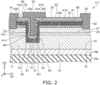
- FIG. 2 is a schematic cross-sectional view illustrating a semiconductor device according to the first embodiment.
- a semiconductor device 111 includes a first compound region 60. Except for this, the configuration of the semiconductor device 111 may be the same as the configuration of the semiconductor device 110.
- the first compound region 60 includes Al and oxygen.
- the first compound region 60 includes, for example, at least one selected from the group consisting of AlO and AlON.
- the first compound region 60 includes a first compound portion 61 and a second compound portion 62.
- the first compound portion 61 is located between the first nitride portion 31 and the first insulating portion 41a.
- the second compound portion 62 is located between the second insulating portion 41b and the second nitride portion 32.
- the first compound region 60 for example, higher carrier mobility can be easily obtained. For example, it becomes easy to obtain a low on-resistance.
- the trap level density at the interface can be reduced. It becomes easy to obtain stable characteristics.
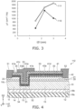
- FIG. 3 is a graph illustrating characteristics of the semiconductor device according to the first embodiment.
- FIG. 3 exemplifies the characteristics of the semiconductor device 110 and the characteristics of the semiconductor device 111.
- the horizontal axis of FIG. 3 is the first nitride partial thickness t31.
- the vertical axis is the carrier mobility ⁇ 1.
- the first compound region 60 is not provided in the semiconductor device 110.
- the first compound region 60 is provided in the semiconductor device 111.
- At least one of the first compound portion 61 or the second compound portion 62 may include an amorphous portion.
- a second compound portion thickness t62 (see FIG. 2 ) along the first direction D1 of the second compound portion 62 may be larger than a first compound portion thickness t61 (see FIG. 2 ) along the second direction D2 of the first compound portion 61.
- the first compound portion thickness t61 is not less than 0.5 nm and not more than 2 nm.
- the second compound portion thickness t62 is 3 nm or less.
- FIG. 4 is a schematic cross-sectional view illustrating a semiconductor device according to the first embodiment.
- the second insulating region 42b is omitted. Except for this, the configuration of the semiconductor device 112 may be the same as the configuration of the semiconductor device 110 or the configuration of the semiconductor device 111.
- the second semiconductor portion 22 contacts the fifth nitride portion 35.
- a high electron carrier concentration is easy to be obtained in the region corresponding to the second semiconductor portion 22. It becomes easy to obtain a low on-resistance.
- a low on-resistance and a high threshold voltage are also obtained in the semiconductor device 112.
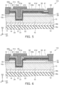
- FIG. 5 is a schematic cross-sectional view illustrating a semiconductor device according to the first embodiment.
- a part of the first nitride region 30 is provided between the first insulating region 42a and the second electrode 52. Except for this, the configuration of the semiconductor device 113 may be the same as the configuration of the semiconductor devices 110-112.
- the semiconductor device 113 for example, current collapse can be suppressed. It is easy to obtain a stable operation. For example, a high carrier concentration can be easily obtained in a region where a part of the first nitride region 30 is provided between the first insulating region 42a and the second electrode 52. It becomes easy to obtain low on-resistance. A low on-resistance and a high threshold voltage can also be obtained in the semiconductor device 113.
- FIG. 6 is a schematic cross-sectional view illustrating a semiconductor device according to the first embodiment.
- a part of the first face F1 (See FIG.1 ) of the first semiconductor portion 21 contacts the first nitride region 30. Another portion of the first face F1 contacts the first insulating region 42a. Except for this, the configuration of the semiconductor device 114 may be the same as the configuration of the semiconductor devices 110-112.
- the part of the first face F1 contacting the first nitride region 30 overlaps a part of the third electrode 53 in the second direction D2.
- a high carrier concentration can be easily obtained in a region where the first face F1 contacting the first nitride region 30. It becomes easy to obtain a low on-resistance. For example, in the portion where the first face F1 contacts the first nitride region 30, it becomes easy to reduce the trap level density at the interface. It becomes easy to obtain stable operation.
- at least a part of the first insulating region 42a may overlap a part of the third electrode 53 in the second direction D2. It becomes easy to obtain a high breakdown voltage. Also in the semiconductor device 114, a high carrier mobility ⁇ 1 and a high threshold voltage are obtained.
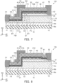
- FIG. 7 is a schematic cross-sectional view illustrating a semiconductor device according to the first embodiment.
- the second semiconductor portion 22 is not provided. Except for this, the configuration of the semiconductor device 115 may be the same as the configuration of the semiconductor devices 110-114.
- the first nitride region 30 further includes a fifth nitride portion 35.
- a direction from the fourth partial region 14 to the fifth nitride portion 35 is along the second direction D2.
- a direction from the fifth nitride portion 35 to the first nitride portion 31 is along the first direction D1.
- a high carrier mobility ⁇ 1 and a high threshold voltage are also obtained in the semiconductor device 115.
- FIG. 8 is a schematic cross-sectional view illustrating a semiconductor device according to the first embodiment.
- the second semiconductor portion 22 is also not provided.
- semiconductor device 116 a part of the first nitride region 30 is provided between first insulating region 42a and second electrode 52. Except for this, the configuration of the semiconductor device 116 may be the same as the configuration of the semiconductor device 115. A high carrier mobility ⁇ 1 and a high threshold voltage are also obtained in the semiconductor device 116. It becomes easy to obtain stable operation that suppresses current collapse.
- FIG. 9 is a schematic cross-sectional view illustrating a semiconductor device according to a second embodiment.
- a semiconductor device 120 includes a first electrode 51, a second electrode 52, a third electrode 53, a first semiconductor region 10, a second semiconductor region 20, a first nitride region 30, and a first insulating member 41.
- the direction from the first electrode 51 to the second electrode 52 is along the first direction D1.
- the third electrode 53 includes the first electrode portion 53a.
- the position of the third electrode 53 in the first direction D1 is between the position of the first electrode 51 in the first direction D1 and the position of the second electrode 52 in the first direction D1.
- the first semiconductor region 10 includes Al x1 Ga 1-x1 N (0 ⁇ x1 ⁇ 1).
- the first semiconductor region 10 includes the first partial region 11, the second partial region 12, the third partial region 13, the fourth partial region 14, and the fifth partial region 15.
- the second direction D2 from the first partial region 11 to the first electrode 51 crosses the first direction D1.
- the direction from the second partial region 12 to the second electrode 52 is along the second direction D2.
- the direction from the third partial region 13 to the first electrode portion 53a is along the second direction D2.
- the position of the fourth partial region 14 in the first direction D1 is between the position of the first partial region 11 in the first direction D1 and the position of the third partial region 13 in the first direction D1.
- the position of the fifth partial region 15 in the first direction D1 is between the position of the third partial region 13 in the first direction D1 and the position of the second partial region 12 in the first direction D1.
- the second semiconductor region 20 includes Al x2 Ga 1-x2 N (0 ⁇ x2 ⁇ 1, x1 ⁇ x2).
- the second semiconductor region 20 includes the first semiconductor portion 21.
- the direction from the fifth partial region 15 to the first semiconductor portion 21 is along the second direction D2.
- the first nitride region 30 includes Al and N.
- the first nitride region 30 includes the first nitride portion 31.
- the first nitride portion 31 is located between the third partial region 13 and the first electrode portion 53a in the second direction D2.
- the direction from the first nitride portion 31 to the fifth partial region 15 is along the first direction D1.
- the first insulating member 41 includes the first insulating portion 41a and the second insulating portion 41b.
- the first insulating portion 41a is located between the first nitride portion 31 and the first electrode portion 53a.
- the direction from at least a part of the first insulating portion 41a to the first semiconductor portion 21 is along the first direction D1.
- the second insulating portion 41b contacts the fifth partial region 15.
- the direction from a part of the second insulating portion 41b to the fifth partial region 15 is along the first direction D1.
- the direction from other portion of the second insulating portion 41b to the first semiconductor portion 21 is along the first direction D1.
- the other portion of the second insulating portion 41b contacts the first semiconductor portion 21.
- the first insulating member 41 includes the first insulating portion 41a and the second insulating portion 41b.
- a high carrier mobility ⁇ 1 can be obtained.
- a high threshold voltage can be obtained.
- a semiconductor device with improved characteristics can be provided.
- the first nitride region 30 includes, for example, Al z1 Ga 1-z1 N (0 ⁇ z1 ⁇ 1, x2 ⁇ z1).
- the composition ratio x2 in the second semiconductor region 20 is, for example, not less than 0.1 and not more than 0.35.
- the composition ratio z1 in the first nitride region 30 is not less than 0.6 and no more than 1.
- the second semiconductor region 20 includes the second semiconductor portion 22.
- the configuration described with respect to the first embodiment may be applied to the semiconductor device 120.
- FIG. 10 is a schematic cross-sectional view illustrating a semiconductor device according to the second embodiment.
- the second semiconductor portion 22 is omitted. Except for this, the configuration of the semiconductor device 121 may be the same as the configuration of the semiconductor device 120.
- the first nitride region 30 further includes the fifth nitride portion 35.
- the direction from the fourth partial region 14 to the fifth nitride portion 35 is along the second direction D2.
- the direction from the fifth nitride portion 35 to the first nitride portion 31 is along the first direction D1. Also in the semiconductor device 121, a high carrier mobility ⁇ 1 and a high threshold voltage are obtained.
- the third embodiment relates to a method of manufacturing a semiconductor device.
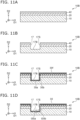
- FIGS. 11A to 11D and 12A to 12C are schematic cross-sectional views illustrating the method for manufacturing a semiconductor device according to the third embodiment.
- a structure 10B is prepared.
- the structure 10B includes the first semiconductor region 10 including Al x1 Ga 1-x1 N (0 ⁇ x1 ⁇ 1) and the second semiconductor region 20 including Al x2 Ga 1-x2 N (0 ⁇ x2 ⁇ 1, x1 ⁇ x2).
- the second semiconductor region 20 is provided on the first semiconductor region 10.
- the structure 10B includes second insulating member 42.
- the second insulating member 42 is provided on the second semiconductor region 20.
- a recess 17 are formed in the structure 10B.
- the recess 17 can be formed by etching using a mask.
- the structure 10B may include a recess 17.
- the recess 17 extends in a direction from the second semiconductor region 20 to first semiconductor region 10. A portion of the first semiconductor region 10 is exposed at a bottom 17B of the recess 17.
- the second semiconductor region 20 is exposed at the side portion 17S of the recess 17.
- a film 30f including Al and N is formed inside the recess 17.
- the film 30f can be formed by epitaxial growth.
- the film 30f includes a first film portion 30a and a second film portion 30b.
- the first film portion 30a is provided on the bottom 17B of the recess 17.
- the second film portion 30b is provided on the side portion 17S of the recess 17.
- the thickness t30b of the second film portion 30b is made thinner than the thickness t30a of the first film portion 30a.
- an additional film is selectively formed on the portion corresponding to the bottom 17B of the recess 17. Thereby, a difference in thickness is obtained.
- a part of the film 30f corresponding to the side portion 17S of the recess 17 is selectively removed. Thereby, a difference in thickness is obtained.
- the growth mode and growth conditions of the film 30f are controlled. For example, different growth rates can be obtained depending on the crystal orientation.
- a thickness difference is obtained by controlling the growth method and the growth condition.
- heat treatment or the like is performed. Thereby, the thickness t30a of the second film portion 30b decreases from the thickness before heating.
- the thickness difference is obtained by various methods. The first nitride region 30 having a difference in thickness is obtained.
- the semiconductor device according to the embodiment is obtained.
- the embodiments may include the following configurations (for example, technical proposals).
- a semiconductor device comprising:
- the first insulating member includes at least one selected from the group consisting of SiO 2 , SiON, AlSiON, AlON and Al 2 O 3 .
- the semiconductor device comprising:
- a method for manufacturing a semiconductor device comprising:
- a semiconductor device capable of improving characteristics and a method of manufacturing the same are provided.
Landscapes
- Junction Field-Effect Transistors (AREA)
- Electrodes Of Semiconductors (AREA)
- Insulated Gate Type Field-Effect Transistor (AREA)
Abstract
A semiconductor device includes a first electrode (51), a second electrode (52), a third electrode (53), a first semiconductor region (10), a second semiconductor region (20), a first nitride region (30), and a first insulating member (41). The first semiconductor region includes Alx1Ga1-x1N (0 ≤ x1 < 1). The second semiconductor region includes Alx2Ga1-x2N (0 < x2 < 1, x1 < x2). A first nitride portion thickness (t31) along a second direction of the first nitride portion is thicker than a second nitride portion thickness (t32) along the first direction of the part of the second nitride portion. A first semiconductor portion thickness (t21) along the second direction of the first semiconductor portion is thicker than the first nitride portion thickness.
Description
- Embodiments of the invention generally relate to a semiconductor device and a method for manufacturing the same.
- For example, semiconductor devices are desired to have improved characteristics.
-
-
FIG. 1 is a schematic cross-sectional view illustrating a semiconductor device according to a first embodiment; -
FIG. 2 is a schematic cross-sectional view illustrating a semiconductor device according to the first embodiment; -
FIG. 3 is a graph illustrating characteristics of the semiconductor device according to the first embodiment; -
FIG. 4 is a schematic cross-sectional view illustrating a semiconductor device according to the first embodiment; -
FIG. 5 is a schematic cross-sectional view illustrating a semiconductor device according to the first embodiment; -
FIG. 6 is a schematic cross-sectional view illustrating a semiconductor device according to the first embodiment; -
FIG. 7 is a schematic cross-sectional view illustrating a semiconductor device according to the first embodiment; -
FIG. 8 is a schematic cross-sectional view illustrating a semiconductor device according to the first embodiment; -
FIG. 9 is a schematic cross-sectional view illustrating a semiconductor device according to a second embodiment; -
FIG. 10 is a schematic cross-sectional view illustrating a semiconductor device according to the second embodiment; -
FIGS. 11A to 11D are schematic cross-sectional views illustrating the method for manufacturing a semiconductor device according to a third embodiment; and -
FIGS. 12A to 12C are schematic cross-sectional views illustrating the method for manufacturing the semiconductor device according to the third embodiment. - According to one embodiment, a semiconductor device includes a first electrode, a second electrode, a third electrode, a first semiconductor region, a second semiconductor region, a first nitride region, and a first insulating member. A direction from the first electrode to the second electrode is along a first direction. The third electrode includes a first electrode portion. A position of the third electrode in the first direction being between a position of the first electrode in the first direction and a position of the second electrode in the first direction. The first semiconductor region includes Alx1Ga1-x1N (0 ≤ x1 < 1). The first semiconductor region includes a first partial region, a second partial region, a third partial region, a fourth partial region, and a fifth partial region. A second direction from the first partial region to the first electrode crosses the first direction. A direction from the second partial region to the second electrode is along the second direction. A direction from the third partial region to the first electrode portion is along the second direction. A position of the fourth partial region in the first direction is between a position of the first partial region in the first direction and a position of the third partial region in the first direction. A position of the fifth partial region in the first direction is between the position of the third partial region in the first direction and a position of the second partial region in the first direction. The second semiconductor region includes Alx2Ga1-x2N (0 < x2 < 1, x1 < x2). The second semiconductor region includes a first semiconductor portion. A direction from the fifth partial region to the first semiconductor portion is along the second direction. The first nitride region includes Al and N. The first nitride region includes a first nitride portion and a second nitride portion. The first nitride portion is located between the third partial region and the first electrode portion in the second direction. The first insulating member includes a first insulating portion and a second insulating portion. The first insulating portion is located between the first nitride portion and the first electrode portion. A part of the second nitride portion is located between the first insulating portion and the fifth partial region in the first direction. Another part of the second nitride portion is located between the second insulating portion and the first semiconductor portion. A first nitride portion thickness along the second direction of the first nitride portion is thicker than a second nitride portion thickness along the first direction of the part of the second nitride portion. A first semiconductor portion thickness along the second direction of the first semiconductor portion is thicker than the first nitride portion thickness.
- Various embodiments are described below with reference to the accompanying drawings.
- The drawings are schematic and conceptual; and the relationships between the thickness and width of portions, the proportions of sizes among portions, etc., are not necessarily the same as the actual values. The dimensions and proportions may be illustrated differently among drawings, even for identical portions.
- In the specification and drawings, components similar to those described previously in an antecedent drawing are marked with like reference numerals, and a detailed description is omitted as appropriate.
-
FIG. 1 is a schematic cross-sectional view illustrating a semiconductor device according to a first embodiment. - As shown in
FIG. 1 , asemiconductor device 110 according to the embodiment includes afirst electrode 51, asecond electrode 52, athird electrode 53, afirst semiconductor region 10, asecond semiconductor region 20, afirst nitride region 30, and a firstinsulating member 41. - A direction from the
first electrode 51 to thesecond electrode 52 is along a first direction D1. The first direction D1 is defined as an X-axis direction. One direction perpendicular to the X-axis direction is defined as a Z-axis direction. A direction perpendicular to the X-axis direction and the Z-axis direction is defined as a Y-axis direction. - The
third electrode 53 includes afirst electrode portion 53a. A position of thethird electrode 53 in the first direction D1 is between a position of thefirst electrode 51 in the first direction D1 and a position of thesecond electrode 52 in the first direction D1. - The
first semiconductor region 10 includes Alx1Ga1-x1N (0 ≤ x1 < 1). The composition ratio x1 may be, for example, not less than 0 and not more than 0.1. Thefirst semiconductor region 10 is, for example, a GaN layer. - The
first semiconductor region 10 includes a firstpartial region 11, a secondpartial region 12, a thirdpartial region 13, a fourthpartial region 14 and a fifthpartial region 15. A second direction D2 from the firstpartial region 11 to thefirst electrode 51 crosses the first direction D1. The second direction D2 is, for example, the Z-axis direction. - A direction from the second
partial region 12 to thesecond electrode 52 is along the second direction D2. A direction from the thirdpartial region 13 to thefirst electrode portion 53a is along the second direction D2. A position of the fourthpartial region 14 in the first direction D1 is between a position of the firstpartial region 11 in the first direction D1 and a position of the thirdpartial region 13 in the first direction D1. A position of the fifthpartial region 15 in the first direction D1 is between the position of the thirdpartial region 13 in the first direction D1 and a position of the secondpartial region 12 in the first direction D1. - The
second semiconductor region 20 includes Alx2Ga1-x2N (0<x2<1, x1<x2). The composition ratio x2 is, for example, more than 0.1 and not more than 0.35. Thesecond semiconductor region 20 is, for example, an AlGaN layer. Thesecond semiconductor region 20 includes afirst semiconductor portion 21. A direction from the fifthpartial region 15 to thefirst semiconductor portion 21 is along the second direction D2. - The
first nitride region 30 includes Al and N. Thefirst nitride region 30 may be AlN, for example. Thefirst nitride region 30 includes afirst nitride portion 31 and asecond nitride portion 32. Thefirst nitride portion 31 is located between the thirdpartial region 13 and thefirst electrode portion 53a in the second direction D2. A direction from a part of thesecond nitride portion 32 to the fifthpartial region 15 is along the first direction D1. A direction from another part of thesecond nitride portion 32 to thefirst semiconductor portion 21 is along the first direction D1. - A first nitride portion thickness t31 of the
first nitride portion 31 along the second direction D2 is thicker than a second nitride portion thickness t32 of thesecond nitride portion 32 along the first direction D1. A first semiconductor portion thickness t21 along the second direction D2 of thefirst semiconductor portion 21 is thicker than the first nitride portion thickness t31. - The first insulating
member 41 includes a first insulatingportion 41a and a second insulatingportion 41b. The first insulatingportion 41a is located between thefirst nitride portion 31 and thefirst electrode portion 53a. The second insulatingportion 41b is located between thefirst electrode portion 53a and thesecond nitride portion 32. A part of thesecond nitride portion 32 is located between the first insulatingportion 41a and the fifthpartial region 15 in the first direction D1. The other part of thesecond nitride portion 32 is located between the second insulatingportion 41b and thefirst semiconductor portion 21. - In this example, the
second semiconductor region 20 further includes asecond semiconductor portion 22. A direction from the fourthpartial region 14 to thesecond semiconductor portion 22 is along the second direction D2. In this example, thefirst electrode portion 53a is located between thefirst semiconductor portion 21 and thesecond semiconductor portion 22 in the first direction D1. - In the
semiconductor device 110, a current flowing between thefirst electrode 51 and thesecond electrode 52 can be controlled by a potential of thethird electrode 53. The potential of thethird electrode 53 is, for example, a potential based on a potential of thefirst electrode 51. Thefirst electrode 51 is, for example, a source electrode. Thesecond electrode 52 is, for example, a drain electrode. Thethird electrode 53 is, for example, a gate electrode. Thesemiconductor device 110 is, for example, a transistor. - The
first semiconductor region 10 includes a region facing thesecond semiconductor region 20. Acarrier region 10c is formed in this region. Thesemiconductor device 110 is, for example, a HEMT (High Electron Mobility Transistor). - A distance between the
first electrode 51 and thethird electrode 53 is shorter than a distance between thesecond electrode 52 and thethird electrode 53. It becomes easy to obtain stable operation. - As noted above, the first nitride portion thickness t31 is thicker than the second nitride portion thickness t32. By the first nitride portion thickness t31 being thick, for example, high mobility can be obtained. By the second nitride portion thickness t32 being thin, it becomes easy to obtain, for example, a high threshold voltage. According to the embodiments, it is possible to provide a semiconductor device with improved characteristics.
- In the embodiment, the
first nitride region 30 is provided apart from thefirst semiconductor portion 21 of thesecond semiconductor region 20. This makes it easy to obtain stable operation. For example, by providing thefirst nitride region 30, it is possible to suppress the intrusion of impurities from the outside into thesecond semiconductor region 20 during the manufacturing process. - By the first nitride portion thickness t31 being thinner than the first semiconductor portion thickness t21, for example, the Al composition ratio in the
first nitride region 30 can be increased. This makes it easy to obtain a high carrier concentration. High mobility is easily obtained. For example, the time required for the manufacturing process can be shortened. - In the embodiment, at least a part of the first insulating
portion 41a is located between the fourthpartial region 14 and the fifthpartial region 15 in the first direction D1. For example, a normally-off characteristic can be obtained. - For example, in a first configuration, the first nitride portion thickness t31 is 2 nm and the second nitride portion thickness t32 is 2 nm. In the first configuration, the channel mobility is 790 cm2/Vs. The threshold voltage is 1.5V.
- For example, in a second configuration, the first nitride portion thickness t31 is 2 nm and the second nitride portion thickness t32 is 1.8 nm. In the second configuration, the channel mobility is 800 cm2/Vs. The threshold voltage is 2.1V.
- In the embodiment, the first nitride partial thickness t31 is preferably not less than 1 nm and not more 10 nm, for example. For example, the Al composition ratio of the
first nitride region 30 can be increased. High carrier mobility is easily obtained. For example, it becomes easy to obtain high crystallinity. Leak current caused by grain boundaries can be suppressed. Leak current can be reduced. - In the embodiment, the second nitride partial thickness t32 is preferably not less than 0.5 nm and not more than 5 nm, for example. For example, it becomes easy to obtain the
second nitride portion 32 being stable. For example, it becomes easy to obtain a high threshold voltage. For example, it becomes easy to obtain high crystallinity. Leak current caused by grain boundaries can be suppressed. Leak current can be reduced. - In the embodiment, the first semiconductor portion thickness t21 is preferably not less than 15 nm and not more than 40 nm, for example. For example, it becomes easy to control the carrier concentration. It becomes easy to obtain stable characteristics. For example, it becomes easy to obtain high crystallinity. Leak current caused by grain boundaries can be suppressed. Leak current can be reduced.
- In the embodiment, for example, the
first nitride portion 31 includes Alz1Ga1-z1N (0 < z1 < 1, x2 < z1. Thesecond nitride portion 32 includes Alz2Ga1-z2N (0 < z2 ≤ 1, z1 < z2). - In the
second semiconductor region 20, the composition ratio x2 is, for example, not less than 0.1 and not more than 0.35. In one example, the composition ratio z1 is not less than 0.6 and less than 1, for example. For example, the composition ratio z1 may be not less than 0.6 and not more than 0.98. At this time, the composition ratio z2 is more than 0.98 and not more than 1, for example. - As shown in
FIG. 1 , the thirdpartial region 13 includes a first facing face Fa1. The first facing face Fa1 faces thefirst nitride portion 31. Thefirst semiconductor portion 21 includes a first face F1 and a second face F2. The second face F2 faces the fifthpartial region 15. The second face F2 is located between the fifthpartial region 15 and the first face F1 in the second direction D2. - A distance along the second direction D2 between a position of the first facing face Fa1 in the second direction D2 and a position of the first face F1 in the second direction D2 is defined as a distance d1. In the embodiment, the distance d1 is preferably not less than 100 nm and not more than 400 nm. For example, when the distance d1 is 100 nm or more, it becomes easy to obtain an appropriately high threshold voltage. For example, when the distance d1 is 400 nm or less, it becomes easy to obtain a low on-resistance. A high threshold voltage and a low on-resistance are easily obtained.
- The first insulating
member 41 includes, for example, at least one selected from the group consisting of SiO2, SiON, AlSiON, AlON and Al2O3. - As shown in
FIG. 1 , thesemiconductor device 110 may include a second insulatingmember 42. The second insulatingmember 42 includes a firstinsulating region 42a. Thefirst semiconductor portion 21 is located between the fifthpartial region 15 and the firstinsulating region 42a. The second insulatingmember 42 functions, for example, as a protective film. Current collapse can be reduced. It becomes easy to obtain stable operation. For example, it becomes easy to obtain a high breakdown voltage. - The second insulating
member 42 includes, for example, at least one selected from the group consisting of SiN, SiO2, SiON, AlSiON, AlON and Al2O3. - As shown in
FIG. 1 , thefirst nitride region 30 may further include athird nitride portion 33. Thefirst semiconductor portion 21 is located between the fifthpartial region 15 and thethird nitride portion 33. A third nitride portion thickness t33 along the second direction D2 of thethird nitride portion 33 may be thicker than the second nitride portion thickness t32. By the third nitride partial thickness t33 being thicker than the second nitride partial thickness t32, for example, it is possible to more effectively suppress the intrusion of impurities from the outside into thesecond semiconductor region 20 during the manufacturing process. - As shown in
FIG. 1 , thefirst nitride region 30 may further include afourth nitride portion 34. A part of thefourth nitride portion 34 is located between the fourthpartial region 14 and the first insulatingportion 41a in the first direction D1. The first nitride portion thickness t31 is thicker than a fourth nitride portion thickness t34 of the part of thefourth nitride portion 34 along the first direction D1. The second semiconductor portion thickness t22 along the second direction D2 of thesecond semiconductor portion 22 is thicker than the first nitride portion thickness t31. - The first insulating
member 41 further includes a third insulatingportion 41c. For example, at least a part of the third insulatingportion 41c is located between the part of thefourth nitride portion 34 and the first insulatingportion 41a. For example, at least a part of the third insulatingportion 41c may be located between thefourth nitride portion 34 and thefirst electrode portion 53a. Another part of thefourth nitride portion 34 is located between thesecond semiconductor portion 22 and the third insulatingportion 41c in the first direction D1. - As shown in
FIG. 1 , thefirst nitride region 30 may further include athird nitride portion 33 and afifth nitride portion 35. Thefirst semiconductor portion 21 is located between the fifthpartial region 15 and thethird nitride portion 33. As already explained, the third nitride portion thickness t33 along the second direction D2 of thethird nitride portion 33 is thicker than the second nitride portion thickness t32. - The
second semiconductor portion 22 is located between the fourthpartial region 14 and thefifth nitride portion 35. A fifth nitride portion thickness t35 along the second direction D2 of thefifth nitride portion 35 is thicker than the second nitride portion thickness t32. - The first insulating
member 41 may further include a fourth insulatingportion 41d and a fifth insulatingportion 41e. Thefirst semiconductor portion 21 is located between the fifthpartial region 15 and the fourth insulatingportion 41d in the second direction D2. Thesecond semiconductor portion 22 is located between the fourthpartial region 14 and the fifth insulatingportion 41e in the second direction D2. - The second insulating
member 42 may include a secondinsulating region 42b. Thesecond semiconductor portion 22 is located between the fourthpartial region 14 and the secondinsulating region 42b in the second direction D2. - The
semiconductor device 110 may include abase body 18s and anitride layer 18b. Thebase body 18s may be, for example, a silicon substrate. Thenitride layer 18b is provided on thebase body 18s. Thefirst semiconductor region 10 is provided on thenitride layer 18b. Thesecond semiconductor region 20 is provided on thefirst semiconductor region 10. -
FIG. 2 is a schematic cross-sectional view illustrating a semiconductor device according to the first embodiment. - As shown in
FIG. 2 , asemiconductor device 111 according to the embodiment includes afirst compound region 60. Except for this, the configuration of thesemiconductor device 111 may be the same as the configuration of thesemiconductor device 110. - The
first compound region 60 includes Al and oxygen. Thefirst compound region 60 includes, for example, at least one selected from the group consisting of AlO and AlON. - The
first compound region 60 includes afirst compound portion 61 and asecond compound portion 62. Thefirst compound portion 61 is located between thefirst nitride portion 31 and the first insulatingportion 41a. Thesecond compound portion 62 is located between the second insulatingportion 41b and thesecond nitride portion 32. - By providing the
first compound region 60, for example, higher carrier mobility can be easily obtained. For example, it becomes easy to obtain a low on-resistance. By providing thefirst compound region 60, for example, the trap level density at the interface can be reduced. It becomes easy to obtain stable characteristics. -
FIG. 3 is a graph illustrating characteristics of the semiconductor device according to the first embodiment. -
FIG. 3 exemplifies the characteristics of thesemiconductor device 110 and the characteristics of thesemiconductor device 111. The horizontal axis ofFIG. 3 is the first nitride partial thickness t31. The vertical axis is the carrier mobility µ1. Thefirst compound region 60 is not provided in thesemiconductor device 110. Thefirst compound region 60 is provided in thesemiconductor device 111. - As shown in
FIG. 3 , in thesemiconductor device 111, a carrier mobility µ1 higher than that in thesemiconductor device 110 is obtained. - In the
semiconductor device 111, at least one of thefirst compound portion 61 or thesecond compound portion 62 may include an amorphous portion. - A second compound portion thickness t62 (see
FIG. 2 ) along the first direction D1 of thesecond compound portion 62 may be larger than a first compound portion thickness t61 (seeFIG. 2 ) along the second direction D2 of thefirst compound portion 61. - For example, the first compound portion thickness t61 is not less than 0.5 nm and not more than 2 nm. For example, the second compound portion thickness t62 is 3 nm or less.
-
FIG. 4 is a schematic cross-sectional view illustrating a semiconductor device according to the first embodiment. - As shown in
FIG. 4 , in asemiconductor device 112 according to the embodiment, the secondinsulating region 42b is omitted. Except for this, the configuration of thesemiconductor device 112 may be the same as the configuration of thesemiconductor device 110 or the configuration of thesemiconductor device 111. - In the
semiconductor device 112, thesecond semiconductor portion 22 contacts thefifth nitride portion 35. A high electron carrier concentration is easy to be obtained in the region corresponding to thesecond semiconductor portion 22. It becomes easy to obtain a low on-resistance. A low on-resistance and a high threshold voltage are also obtained in thesemiconductor device 112. -
FIG. 5 is a schematic cross-sectional view illustrating a semiconductor device according to the first embodiment. - As shown in
FIG. 5 , in asemiconductor device 113 according to the embodiment, a part of thefirst nitride region 30 is provided between the firstinsulating region 42a and thesecond electrode 52. Except for this, the configuration of thesemiconductor device 113 may be the same as the configuration of the semiconductor devices 110-112. - In the
semiconductor device 113, for example, current collapse can be suppressed. It is easy to obtain a stable operation. For example, a high carrier concentration can be easily obtained in a region where a part of thefirst nitride region 30 is provided between the firstinsulating region 42a and thesecond electrode 52. It becomes easy to obtain low on-resistance. A low on-resistance and a high threshold voltage can also be obtained in thesemiconductor device 113. -
FIG. 6 is a schematic cross-sectional view illustrating a semiconductor device according to the first embodiment. - As shown in
FIG. 6 , in asemiconductor device 114 according to the embodiment, a part of the first face F1 (SeeFIG.1 ) of thefirst semiconductor portion 21 contacts thefirst nitride region 30. Another portion of the first face F1 contacts the firstinsulating region 42a. Except for this, the configuration of thesemiconductor device 114 may be the same as the configuration of the semiconductor devices 110-112. - In the
semiconductor device 114, the part of the first face F1 contacting thefirst nitride region 30 overlaps a part of thethird electrode 53 in the second direction D2. In thesemiconductor device 114, for example, a high carrier concentration can be easily obtained in a region where the first face F1 contacting thefirst nitride region 30. It becomes easy to obtain a low on-resistance. For example, in the portion where the first face F1 contacts thefirst nitride region 30, it becomes easy to reduce the trap level density at the interface. It becomes easy to obtain stable operation. In thesemiconductor device 114, at least a part of the firstinsulating region 42a may overlap a part of thethird electrode 53 in the second direction D2. It becomes easy to obtain a high breakdown voltage. Also in thesemiconductor device 114, a high carrier mobility µ1 and a high threshold voltage are obtained. -
FIG. 7 is a schematic cross-sectional view illustrating a semiconductor device according to the first embodiment. - As shown in
FIG. 7 , in asemiconductor device 115 according to the embodiment, thesecond semiconductor portion 22 is not provided. Except for this, the configuration of thesemiconductor device 115 may be the same as the configuration of the semiconductor devices 110-114. - In the
semiconductor device 115, thefirst nitride region 30 further includes afifth nitride portion 35. A direction from the fourthpartial region 14 to thefifth nitride portion 35 is along the second direction D2. A direction from thefifth nitride portion 35 to thefirst nitride portion 31 is along the first direction D1. A high carrier mobility µ1 and a high threshold voltage are also obtained in thesemiconductor device 115. -
FIG. 8 is a schematic cross-sectional view illustrating a semiconductor device according to the first embodiment. - As shown in
FIG. 8 , in thesemiconductor device 116 according to the embodiment, thesecond semiconductor portion 22 is also not provided. Insemiconductor device 116, a part of thefirst nitride region 30 is provided between firstinsulating region 42a andsecond electrode 52. Except for this, the configuration of thesemiconductor device 116 may be the same as the configuration of thesemiconductor device 115. A high carrier mobility µ1 and a high threshold voltage are also obtained in thesemiconductor device 116. It becomes easy to obtain stable operation that suppresses current collapse. -
FIG. 9 is a schematic cross-sectional view illustrating a semiconductor device according to a second embodiment. - As shown in
FIG. 9 , asemiconductor device 120 according to the embodiment includes afirst electrode 51, asecond electrode 52, athird electrode 53, afirst semiconductor region 10, asecond semiconductor region 20, afirst nitride region 30, and a first insulatingmember 41. - The direction from the
first electrode 51 to thesecond electrode 52 is along the first direction D1. Thethird electrode 53 includes thefirst electrode portion 53a. The position of thethird electrode 53 in the first direction D1 is between the position of thefirst electrode 51 in the first direction D1 and the position of thesecond electrode 52 in the first direction D1. - The
first semiconductor region 10 includes Alx1Ga1-x1N (0 ≤ x1 < 1). Thefirst semiconductor region 10 includes the firstpartial region 11, the secondpartial region 12, the thirdpartial region 13, the fourthpartial region 14, and the fifthpartial region 15. The second direction D2 from the firstpartial region 11 to thefirst electrode 51 crosses the first direction D1. The direction from the secondpartial region 12 to thesecond electrode 52 is along the second direction D2. The direction from the thirdpartial region 13 to thefirst electrode portion 53a is along the second direction D2. The position of the fourthpartial region 14 in the first direction D1 is between the position of the firstpartial region 11 in the first direction D1 and the position of the thirdpartial region 13 in the first direction D1. The position of the fifthpartial region 15 in the first direction D1 is between the position of the thirdpartial region 13 in the first direction D1 and the position of the secondpartial region 12 in the first direction D1. - The
second semiconductor region 20 includes Alx2Ga1-x2N (0 < x2 < 1, x1 < x2). Thesecond semiconductor region 20 includes thefirst semiconductor portion 21. The direction from the fifthpartial region 15 to thefirst semiconductor portion 21 is along the second direction D2. - The
first nitride region 30 includes Al and N. Thefirst nitride region 30 includes thefirst nitride portion 31. Thefirst nitride portion 31 is located between the thirdpartial region 13 and thefirst electrode portion 53a in the second direction D2. For example, the direction from thefirst nitride portion 31 to the fifthpartial region 15 is along the first direction D1. - The first insulating
member 41 includes the first insulatingportion 41a and the second insulatingportion 41b. The first insulatingportion 41a is located between thefirst nitride portion 31 and thefirst electrode portion 53a. The direction from at least a part of the first insulatingportion 41a to thefirst semiconductor portion 21 is along the first direction D1. The second insulatingportion 41b contacts the fifthpartial region 15. The direction from a part of the second insulatingportion 41b to the fifthpartial region 15 is along the first direction D1. The direction from other portion of the second insulatingportion 41b to thefirst semiconductor portion 21 is along the first direction D1. For example, the other portion of the second insulatingportion 41b contacts thefirst semiconductor portion 21. - The first insulating
member 41 includes the first insulatingportion 41a and the second insulatingportion 41b. In thesemiconductor device 120, by providing thefirst nitride portion 31, a high carrier mobility µ1 can be obtained. By the second insulatingportion 41b contacting the fifthpartial region 15, for example, a high threshold voltage can be obtained. According to thesemiconductor device 120, a semiconductor device with improved characteristics can be provided. - In the
semiconductor device 120, thefirst nitride region 30 includes, for example, Alz1Ga1-z1N (0 < z1 <1, x2 < z1). The composition ratio x2 in thesecond semiconductor region 20 is, for example, not less than 0.1 and not more than 0.35. The composition ratio z1 in thefirst nitride region 30 is not less than 0.6 and no more than 1. - In the
semiconductor device 120, thesecond semiconductor region 20 includes thesecond semiconductor portion 22. The configuration described with respect to the first embodiment may be applied to thesemiconductor device 120. -
FIG. 10 is a schematic cross-sectional view illustrating a semiconductor device according to the second embodiment. - As shown in
FIG. 10 , in thesemiconductor device 121 according to the embodiment, thesecond semiconductor portion 22 is omitted. Except for this, the configuration of thesemiconductor device 121 may be the same as the configuration of thesemiconductor device 120. - In the
semiconductor device 121, thefirst nitride region 30 further includes thefifth nitride portion 35. The direction from the fourthpartial region 14 to thefifth nitride portion 35 is along the second direction D2. The direction from thefifth nitride portion 35 to thefirst nitride portion 31 is along the first direction D1. Also in thesemiconductor device 121, a high carrier mobility µ1 and a high threshold voltage are obtained. - The third embodiment relates to a method of manufacturing a semiconductor device.
-
FIGS. 11A to 11D and12A to 12C are schematic cross-sectional views illustrating the method for manufacturing a semiconductor device according to the third embodiment. - As shown in
FIG. 11A , astructure 10B is prepared. Thestructure 10B includes thefirst semiconductor region 10 including Alx1Ga1-x1N (0 ≤ x1<1) and thesecond semiconductor region 20 including Alx2Ga1-x2N (0 < x2 <1, x1 < x2). Thesecond semiconductor region 20 is provided on thefirst semiconductor region 10. In this example, thestructure 10B includes second insulatingmember 42. The second insulatingmember 42 is provided on thesecond semiconductor region 20. - As shown in
FIG. 11B , arecess 17 are formed in thestructure 10B. For example, therecess 17 can be formed by etching using a mask. Thestructure 10B may include arecess 17. Therecess 17 extends in a direction from thesecond semiconductor region 20 tofirst semiconductor region 10. A portion of thefirst semiconductor region 10 is exposed at a bottom 17B of therecess 17. Thesecond semiconductor region 20 is exposed at theside portion 17S of therecess 17. - As shown in
FIG. 11C , afilm 30f including Al and N is formed inside therecess 17. For example, thefilm 30f can be formed by epitaxial growth. Thefilm 30f includes afirst film portion 30a and asecond film portion 30b. Thefirst film portion 30a is provided on the bottom 17B of therecess 17. Thesecond film portion 30b is provided on theside portion 17S of therecess 17. - As shown in
FIG. 11D , the thickness t30b of thesecond film portion 30b is made thinner than the thickness t30a of thefirst film portion 30a. - In one example, after forming a film having a uniform thickness, an additional film is selectively formed on the portion corresponding to the bottom 17B of the
recess 17. Thereby, a difference in thickness is obtained. In another example, after thefilm 30f having a uniform thickness is formed, a part of thefilm 30f corresponding to theside portion 17S of therecess 17 is selectively removed. Thereby, a difference in thickness is obtained. - In another example, the growth mode and growth conditions of the
film 30f are controlled. For example, different growth rates can be obtained depending on the crystal orientation. A thickness difference is obtained by controlling the growth method and the growth condition. In another example, after thefilm 30f having a uniform thickness is formed, heat treatment or the like is performed. Thereby, the thickness t30a of thesecond film portion 30b decreases from the thickness before heating. The thickness difference is obtained by various methods. Thefirst nitride region 30 having a difference in thickness is obtained. - As shown in
FIG. 12A , the first insulatingmember 41 is formed. As shown inFIG. 12 B , thethird electrode 53 is formed. As shown inFIG. 12C , thefirst electrode 51 and thesecond electrode 52 are formed. In this way, the semiconductor device according to the embodiment is obtained. - The embodiments may include the following configurations (for example, technical proposals).
- A semiconductor device, comprising:
- a first electrode;
- a second electrode, a direction from the first electrode to the second electrode being along a first direction;
- a third electrode including a first electrode portion, a position of the third electrode in the first direction being between a position of the first electrode in the first direction and a position of the second electrode in the first direction;
- a first semiconductor region including Alx1Ga1-x1N (0 ≤ x1 < 1), the first semiconductor region including a first partial region, a second partial region, a third partial region, a fourth partial region, and a fifth partial region, a second direction from the first partial region to the first electrode crossing the first direction, a direction from the second partial region to the second electrode being along the second direction, a direction from the third partial region to the first electrode portion being along the second direction, a position of the fourth partial region in the first direction being between a position of the first partial region in the first direction and a position of the third partial region in the first direction, a position of the fifth partial region in the first direction being between the position of the third partial region in the first direction and a position of the second partial region in the first direction;
- a second semiconductor region including Alx2Ga1-x2N (0 < x2 < 1, x1 < x2), the second semiconductor region including a first semiconductor portion, a direction from the fifth partial region to the first semiconductor portion being along the second direction;
- a first nitride region including Al and N, the first nitride region including a first nitride portion and a second nitride portion, the first nitride portion being located between the third partial region and the first electrode portion in the second direction; and
- a first insulating member including a first insulating portion and a second insulating portion, the first insulating portion being located between the first nitride portion and the first electrode portion, a part of the second nitride portion being located between the first insulating portion and the fifth partial region in the first direction, another part of the second nitride portion being located between the second insulating portion and the first semiconductor portion,
- a first nitride portion thickness along the second direction of the first nitride portion being thicker than a second nitride portion thickness along the first direction of the part of the second nitride portion, and
- a first semiconductor portion thickness along the second direction of the first semiconductor portion being thicker than the first nitride portion thickness.
- The semiconductor device according to
Configuration 1, wherein - the second semiconductor region further includes a second semiconductor portion,
- a direction from the fourth partial region to the second semiconductor portion is along the second direction, and
- the first electrode portion is located between the first semiconductor portion and the second semiconductor portion in the first direction.
- The semiconductor device according to
Configuration - the first semiconductor portion thickness is not less than 15 nm and note more than 40 nm;
- the first nitride portion thickness is not less than 1 nm and not more than 10 nm, and
- the second nitride portion thickness is not less than 0.5 nm and not more than 5 nm.
- The semiconductor device according to any one of Configurations 1-3, wherein
- the first nitride portion includes Alz1Ga1-z1N (0 < z1 < 1, x 2< z1), and
- the second nitride portion includes Alz2Ga1-z2N (0 < z2 ≤ 1, z1 < z2).
- The semiconductor device according to
Configuration 4, wherein - the x2 is not less than 0.1 and not more than 0.35, and
- the z1 is not less than 0.6 and less than 1.
- The semiconductor device according to Configuration 5, wherein
- the z1 is not less than 0.6 and not more than 0.98, and
- the z2 is more than 0.98 and not more than 1.
- The semiconductor device according to any one of Configurations 1-6, wherein
- the third partial region includes a first facing face,
- the first facing face faces the first nitride portion,
- the first semiconductor portion includes a first face and a second face,
- the second face faces the fifth partial region,
- the second face is located between the fifth partial region and the first face in the second direction, and
- a distance along the second direction between a position of the first facing face in the second direction and a position of the first face in the second direction is not less than 100 nm and not more than 400 nm.
- The semiconductor device according to any one of Configurations 1-7, further comprising:
- a first compound region including Al and oxygen,
- the first compound region including a first compound portion and a second compound portion,
- the first compound portion being located between the first nitride portion and the first insulating portion, and
- the second compound portion being located between the second insulating portion and the second nitride portion.
- The semiconductor device according to Configuration 8, wherein
at least one of the first compound portion or the second compound portion includes an amorphous portion. - The semiconductor device according to Configuration 8 or 9, wherein
a second compound portion thickness along the first direction of the second compound portion is thicker than a first compound portion thickness along the second direction of the first compound portion. - The semiconductor device according to
Configuration 10, wherein
the second compound portion thickness is 3 nm or less. - The semiconductor device according to any one of Configurations 1-11, wherein
the first insulating member includes at least one selected from the group consisting of SiO2, SiON, AlSiON, AlON and Al2O3. - The semiconductor device according to
Configuration 1, further comprising: - a second insulating member including a first insulating region,
- the first semiconductor portion being located between the fifth partial region and the first insulating region, and
- the second insulating member includes at least one selected from the group consisting of SiN, SiO2, SiON, AlSiON, AlON and Al2O3.
- The semiconductor device according to any one of Configurations 1-13, wherein
- the first nitride region further includes a third nitride portion,
- the first semiconductor portion is located between the fifth partial region and the third nitride portion, and
- a third nitride portion thickness along the second direction of the third nitride portion is thicker than the second nitride portion thickness.
- The semiconductor device according to
Configuration 2, wherein - the first nitride region further includes a fourth nitride portion,
- a part of the fourth nitride portion is located between the fourth partial region and the first insulating portion in the first direction,
- the first nitride portion thickness is thicker than a fourth nitride portion thickness along the first direction of the part of the fourth nitride portion,
- a second semiconductor portion thickness along the second direction of the second semiconductor portion is thicker than the first nitride portion thickness,
- the first insulating member further includes a third insulating portion, and
- at least a part of the third insulating portion is located between the part of the fourth nitride portion and the first insulating portion.
- The semiconductor device according to
Configuration 2, wherein - the first nitride region further includes a third nitride portion and a fifth nitride portion,
- the first semiconductor portion is located between the fifth partial region and the third nitride portion,
- a third nitride portion thickness along the second direction of the third nitride portion is thicker than the second nitride portion thickness,
- the second semiconductor portion is located between the fourth partial region and the fifth nitride portion, and
- a fifth nitride portion thickness along the second direction of the fifth nitride portion is thicker than the second nitride portion thickness.
- The semiconductor device according to
Configuration 1, wherein - the first nitride region further includes a fifth nitride portion,
- a direction from the fourth partial region to the fifth nitride portion is along the second direction, and
- a direction from the fifth nitride portion to the first nitride portion is along the first direction.
- The semiconductor device, comprising:
- a first electrode;
- a second electrode, a direction from the first electrode to the second electrode being along a first direction;
- a third electrode including a first electrode portion, a position of the third electrode in the first direction being between a position of the first electrode in the first direction and a position of the second electrode in the first direction;
- a first semiconductor region including Alx1Ga1-x1N (0 ≤ x1 < 1), the first semiconductor region including a first partial region, a second partial region, a third partial region, a fourth partial region, and a fifth partial region, a second direction from the first partial region to the first electrode crossing the first direction, a direction from the second partial region to the second electrode being along the second direction, a direction from the third partial region to the first electrode portion being along the second direction, a position of the fourth partial region in the first direction being between a position of the first partial region in the first direction and a position of the third partial region in the first direction, a position of the fifth partial region in the first direction being between the position of the third partial region in the first direction and a position of the second partial region in the first direction;
- a second semiconductor region including Alx2Ga1-x2N (0 < x2 < 1, x1 < x2), the second semiconductor region including a first semiconductor portion, a direction from the fifth partial region to the first semiconductor portion being along the second direction;
- a first nitride region including Al and N, the first nitride region including a first nitride portion, the first nitride portion being located between the third partial region and the first electrode portion in the second direction; and
- a first insulating member including a first insulating portion and a second insulating portion, the first insulating portion being located between the first nitride portion and the first electrode portion, the second insulating portion contacting the fifth partial region.
- The semiconductor device according to Configuration 18, wherein
- the first nitride region includes Alz1Ga1-z1N (0 < z1 < 1, x2 < z1),
- the x2 is not less than 0.1 and not more than 0.35, and
- the z1 is not less than 0.6 and not more than 1.
- A method for manufacturing a semiconductor device, the method comprising:
- providing a structure, the structure including a first semiconductor region including Alx1Ga1-x1N (0 ≤ x1 < 1), and a second semiconductor region including Alx2Ga1-x2N (0 < x2 < 1, x1 <x 2), the structure including a recess, the recess extends in a direction from the second semiconductor region to the first semiconductor region, a part of the first semiconductor region being exposed at a bottom of the recess;
- forming a film including Al and N inside the recess, the film including a first film portion and a second film portion, the first film portion being provided at the bottom of the recess, the second film portion being provided at a side portion of the recess; and
- making a thickness of the second film portion thinner than a thickness of the first film portion.
- According to the embodiments, a semiconductor device capable of improving characteristics and a method of manufacturing the same are provided.
- Hereinabove, exemplary embodiments of the invention are described with reference to specific examples. However, the embodiments of the invention are not limited to these specific examples. For example, one skilled in the art may similarly practice the invention by appropriately selecting specific configurations of components included in semiconductor devices such as electrodes, semiconductor regions, nitride regions, insulating members, etc., from known art. Such practice is included in the scope of the invention to the extent that similar effects thereto are obtained.
- Further, any two or more components of the specific examples may be combined within the extent of technical feasibility and are included in the scope of the invention to the extent that the purport of the invention is included.
- Moreover, all semiconductor devices and methods of manufacturing the same practicable by an appropriate design modification by one skilled in the art based on the semiconductor devices and methods of manufacturing the same described above as embodiments of the invention also are within the scope of the invention to the extent that the purport of the invention is included.
- Various other variations and modifications can be conceived by those skilled in the art within the spirit of the invention, and it is understood that such variations and modifications are also encompassed within the scope of the invention.
- While certain embodiments have been described, these embodiments have been presented by way of example only, and are not intended to limit the scope of the inventions. Indeed, the novel embodiments described herein may be embodied in a variety of other forms; furthermore, various omissions, substitutions and changes in the form of the embodiments described herein may be made without departing from the spirit of the inventions. The accompanying claims and their equivalents are intended to cover such forms or modifications as would fall within the scope and spirit of the invention.
Claims (15)
- A semiconductor device, comprising:a first electrode;a second electrode, a direction from the first electrode to the second electrode being along a first direction;a third electrode including a first electrode portion, a position of the third electrode in the first direction being between a position of the first electrode in the first direction and a position of the second electrode in the first direction;a first semiconductor region including Alx1Ga1-x1N (0 ≤ x1 < 1), the first semiconductor region including a first partial region, a second partial region, a third partial region, a fourth partial region, and a fifth partial region, a second direction from the first partial region to the first electrode crossing the first direction, a direction from the second partial region to the second electrode being along the second direction, a direction from the third partial region to the first electrode portion being along the second direction, a position of the fourth partial region in the first direction being between a position of the first partial region in the first direction and a position of the third partial region in the first direction, a position of the fifth partial region in the first direction being between the position of the third partial region in the first direction and a position of the second partial region in the first direction;a second semiconductor region including Alx2Ga1-x2N (0 < x2 < 1, x1 < x2), the second semiconductor region including a first semiconductor portion, a direction from the fifth partial region to the first semiconductor portion being along the second direction;a first nitride region including Al and N, the first nitride region including a first nitride portion and a second nitride portion, the first nitride portion being located between the third partial region and the first electrode portion in the second direction; anda first insulating member including a first insulating portion and a second insulating portion, the first insulating portion being located between the first nitride portion and the first electrode portion, a part of the second nitride portion being located between the first insulating portion and the fifth partial region in the first direction, another part of the second nitride portion being located between the second insulating portion and the first semiconductor portion,a first nitride portion thickness along the second direction of the first nitride portion being thicker than a second nitride portion thickness along the first direction of the part of the second nitride portion, anda first semiconductor portion thickness along the second direction of the first semiconductor portion being thicker than the first nitride portion thickness.
- The semiconductor device according to claim 1, whereinthe second semiconductor region further includes a second semiconductor portion,a direction from the fourth partial region to the second semiconductor portion is along the second direction, andthe first electrode portion is located between the first semiconductor portion and the second semiconductor portion in the first direction.
- The semiconductor device according to claim 1 or 2, whereinthe first nitride portion includes Alz1Ga1-z1N (0 < z1 < 1, x 2< z1), andthe second nitride portion includes Alz2Ga1-z2N (0 < z2 ≤ 1, z1 < z2).
- The semiconductor device according to any one of claims 1-3, whereinthe third partial region includes a first facing face,the first facing face faces the first nitride portion,the first semiconductor portion includes a first face and a second face,the second face faces the fifth partial region,the second face is located between the fifth partial region and the first face in the second direction, anda distance along the second direction between a position of the first facing face in the second direction and a position of the first face in the second direction is not less than 100 nm and not more than 400 nm.
- The semiconductor device according to any one of claims 1-4, further comprising:a first compound region including Al and oxygen,the first compound region including a first compound portion and a second compound portion,the first compound portion being located between the first nitride portion and the first insulating portion, andthe second compound portion being located between the second insulating portion and the second nitride portion.
- The semiconductor device according to claim 5, wherein
at least one of the first compound portion or the second compound portion includes an amorphous portion. - The semiconductor device according to claim 5 or 6, wherein
a second compound portion thickness along the first direction of the second compound portion is thicker than a first compound portion thickness along the second direction of the first compound portion. - The semiconductor device according to any one of claims 1-7, wherein
the first insulating member includes at least one selected from the group consisting of SiO2, SiON, AlSiON, AlON and Al2O3. - The semiconductor device according to claim 1, further comprising:a second insulating member including a first insulating region,the first semiconductor portion being located between the fifth partial region and the first insulating region, andthe second insulating member includes at least one selected from the group consisting of SiN, SiO2, SiON, AlSiON, AlON and Al2O3.
- The semiconductor device according to any one of claims 1-9, whereinthe first nitride region further includes a third nitride portion,the first semiconductor portion is located between the fifth partial region and the third nitride portion, anda third nitride portion thickness along the second direction of the third nitride portion is thicker than the second nitride portion thickness.
- The semiconductor device according to claim 2, whereinthe first nitride region further includes a fourth nitride portion,a part of the fourth nitride portion is located between the fourth partial region and the first insulating portion in the first direction,the first nitride portion thickness is thicker than a fourth nitride portion thickness along the first direction of the part of the fourth nitride portion,a second semiconductor portion thickness along the second direction of the second semiconductor portion is thicker than the first nitride portion thickness,the first insulating member further includes a third insulating portion, andat least a part of the third insulating portion is located between the part of the fourth nitride portion and the first insulating portion.
- The semiconductor device according to claim 2, whereinthe first nitride region further includes a third nitride portion and a fifth nitride portion,the first semiconductor portion is located between the fifth partial region and the third nitride portion,a third nitride portion thickness along the second direction of the third nitride portion is thicker than the second nitride portion thickness,the second semiconductor portion is located between the fourth partial region and the fifth nitride portion, anda fifth nitride portion thickness along the second direction of the fifth nitride portion is thicker than the second nitride portion thickness.
- The semiconductor device according to claim 1, whereinthe first nitride region further includes a fifth nitride portion,a direction from the fourth partial region to the fifth nitride portion is along the second direction, anda direction from the fifth nitride portion to the first nitride portion is along the first direction.
- The semiconductor device, comprising:a first electrode;a second electrode, a direction from the first electrode to the second electrode being along a first direction;a third electrode including a first electrode portion, a position of the third electrode in the first direction being between a position of the first electrode in the first direction and a position of the second electrode in the first direction;a first semiconductor region including Alx1Ga1-x1N (0 ≤ x1 < 1), the first semiconductor region including a first partial region, a second partial region, a third partial region, a fourth partial region, and a fifth partial region, a second direction from the first partial region to the first electrode crossing the first direction, a direction from the second partial region to the second electrode being along the second direction, a direction from the third partial region to the first electrode portion being along the second direction, a position of the fourth partial region in the first direction being between a position of the first partial region in the first direction and a position of the third partial region in the first direction, a position of the fifth partial region in the first direction being between the position of the third partial region in the first direction and a position of the second partial region in the first direction;a second semiconductor region including Alx2Ga1-x2N (0 < x2 < 1, x1 < x2), the second semiconductor region including a first semiconductor portion, a direction from the fifth partial region to the first semiconductor portion being along the second direction;a first nitride region including Al and N, the first nitride region including a first nitride portion, the first nitride portion being located between the third partial region and the first electrode portion in the second direction; anda first insulating member including a first insulating portion and a second insulating portion, the first insulating portion being located between the first nitride portion and the first electrode portion, the second insulating portion contacting the fifth partial region.
- A method for manufacturing a semiconductor device, the method comprising:providing a structure, the structure including a first semiconductor region including Alx1Ga1-x1N (0 ≤ x1 < 1), and a second semiconductor region including Alx2Ga1-x2N (0 < x2 < 1, x1 <x 2), the structure including a recess, the recess extends in a direction from the second semiconductor region to the first semiconductor region, a part of the first semiconductor region being exposed at a bottom of the recess;forming a film including Al and N inside the recess, the film including a first film portion and a second film portion, the first film portion being provided at the bottom of the recess, the second film portion being provided at a side portion of the recess; andmaking a thickness of the second film portion thinner than a thickness of the first film portion.
Applications Claiming Priority (1)
| Application Number | Priority Date | Filing Date | Title |
|---|---|---|---|
| JP2023020566A JP2024115088A (en) | 2023-02-14 | 2023-02-14 | Semiconductor device and its manufacturing method |
Publications (1)
| Publication Number | Publication Date |
|---|---|
| EP4418329A1 true EP4418329A1 (en) | 2024-08-21 |
Family
ID=87557743
Family Applications (1)
| Application Number | Title | Priority Date | Filing Date |
|---|---|---|---|
| EP23189868.5A Pending EP4418329A1 (en) | 2023-02-14 | 2023-08-04 | Semiconductor device and method for manufacturing the same |
Country Status (4)
| Country | Link |
|---|---|
| US (1) | US20240274703A1 (en) |
| EP (1) | EP4418329A1 (en) |
| JP (1) | JP2024115088A (en) |
| CN (1) | CN118507509A (en) |
Families Citing this family (1)
| Publication number | Priority date | Publication date | Assignee | Title |
|---|---|---|---|---|
| JP7822561B2 (en) | 2020-09-04 | 2026-03-03 | コーニング インコーポレイテッド | Coated pharmaceutical packaging that blocks ultraviolet light |
Citations (4)
| Publication number | Priority date | Publication date | Assignee | Title |
|---|---|---|---|---|
| US20220045202A1 (en) * | 2020-08-06 | 2022-02-10 | Kabushiki Kaisha Toshiba | Semiconductor device |
| US20220130986A1 (en) * | 2020-10-26 | 2022-04-28 | Kabushiki Kaisha Toshiba | Semiconductor device |
| US20220384629A1 (en) * | 2021-06-01 | 2022-12-01 | Kabushiki Kaisha Toshiba | Semiconductor device |
| US20230025093A1 (en) * | 2021-07-26 | 2023-01-26 | Kabushiki Kaisha Toshiba | Semiconductor device |
Family Cites Families (5)
| Publication number | Priority date | Publication date | Assignee | Title |
|---|---|---|---|---|
| KR20140014778A (en) * | 2012-07-26 | 2014-02-06 | 서울바이오시스 주식회사 | Normally-off nitride-based transistor and method of fabricating the same |
| JP6659283B2 (en) * | 2015-09-14 | 2020-03-04 | 株式会社東芝 | Semiconductor device |
| JP6951301B2 (en) * | 2018-07-23 | 2021-10-20 | 株式会社東芝 | Semiconductor devices and their manufacturing methods |
| JP7362410B2 (en) * | 2019-10-17 | 2023-10-17 | 株式会社東芝 | Manufacturing method of semiconductor device and semiconductor device |
| JP2022184315A (en) * | 2021-06-01 | 2022-12-13 | 株式会社東芝 | Semiconductor device |
-
2023
- 2023-02-14 JP JP2023020566A patent/JP2024115088A/en active Pending
- 2023-08-04 EP EP23189868.5A patent/EP4418329A1/en active Pending
- 2023-08-17 US US18/451,218 patent/US20240274703A1/en active Pending
- 2023-08-21 CN CN202311054496.6A patent/CN118507509A/en active Pending
Patent Citations (4)
| Publication number | Priority date | Publication date | Assignee | Title |
|---|---|---|---|---|
| US20220045202A1 (en) * | 2020-08-06 | 2022-02-10 | Kabushiki Kaisha Toshiba | Semiconductor device |
| US20220130986A1 (en) * | 2020-10-26 | 2022-04-28 | Kabushiki Kaisha Toshiba | Semiconductor device |
| US20220384629A1 (en) * | 2021-06-01 | 2022-12-01 | Kabushiki Kaisha Toshiba | Semiconductor device |
| US20230025093A1 (en) * | 2021-07-26 | 2023-01-26 | Kabushiki Kaisha Toshiba | Semiconductor device |
Also Published As
| Publication number | Publication date |
|---|---|
| US20240274703A1 (en) | 2024-08-15 |
| CN118507509A (en) | 2024-08-16 |
| JP2024115088A (en) | 2024-08-26 |
Similar Documents
| Publication | Publication Date | Title |
|---|---|---|
| US11967641B2 (en) | Semiconductor device including different nitride regions improving characteristics of the semiconductor device | |
| US9406792B2 (en) | Semiconductor device having GaN-based layer | |
| US11088269B2 (en) | Semiconductor device | |
| US7948011B2 (en) | N-polar aluminum gallium nitride/gallium nitride enhancement-mode field effect transistor | |
| US10388779B2 (en) | Semiconductor device and manufacturing method thereof | |
| US9343563B2 (en) | Selectively area regrown III-nitride high electron mobility transistor | |
| CN108400170A (en) | The manufacturing method of semiconductor devices and semiconductor devices | |
| JP2021009989A (en) | Nitride semiconductor device | |
| US20220130986A1 (en) | Semiconductor device | |
| JP7165328B2 (en) | Semiconductor device and method for manufacturing semiconductor device | |
| US20240274703A1 (en) | Semiconductor device and method for manufacturing the same | |
| JP2020177940A (en) | Semiconductor devices and their manufacturing methods | |
| US11699724B2 (en) | Semiconductor device | |
| US10651307B2 (en) | Semiconductor device and method for manufacturing the same | |
| US12543339B2 (en) | Semiconductor device | |
| US20240105828A1 (en) | Nitride semiconductor device and method for manufacturing nitride semiconductor device | |
| US12087823B2 (en) | Semiconductor device | |
| CN118231447A (en) | Enhancement-mode GaN transistors | |
| US20250203909A1 (en) | Semiconductor device | |
| US20240313100A1 (en) | Semiconductor device and method for manufacturing the same | |
| US20250056826A1 (en) | Semiconductor device | |
| JP2016225426A (en) | Semiconductor device and manufacturing method thereof | |
| US12628395B2 (en) | Hemt semiconductor device with a AlInGaN layer for polarity control | |
| JP2026065877A (en) | Nitride semiconductor equipment | |
| CN119521712A (en) | Semiconductor devices |
Legal Events
| Date | Code | Title | Description |
|---|---|---|---|
| PUAI | Public reference made under article 153(3) epc to a published international application that has entered the european phase |
Free format text: ORIGINAL CODE: 0009012 |
|
| STAA | Information on the status of an ep patent application or granted ep patent |
Free format text: STATUS: REQUEST FOR EXAMINATION WAS MADE |
|
| 17P | Request for examination filed |
Effective date: 20230804 |
|
| AK | Designated contracting states |
Kind code of ref document: A1 Designated state(s): AL AT BE BG CH CY CZ DE DK EE ES FI FR GB GR HR HU IE IS IT LI LT LU LV MC ME MK MT NL NO PL PT RO RS SE SI SK SM TR |