EP4415128A1 - Energy storage device and power consuming apparatus - Google Patents
Energy storage device and power consuming apparatus Download PDFInfo
- Publication number
- EP4415128A1 EP4415128A1 EP23212544.3A EP23212544A EP4415128A1 EP 4415128 A1 EP4415128 A1 EP 4415128A1 EP 23212544 A EP23212544 A EP 23212544A EP 4415128 A1 EP4415128 A1 EP 4415128A1
- Authority
- EP
- European Patent Office
- Prior art keywords
- energy storage
- storage device
- current collecting
- lower plastic
- grid structure
- Prior art date
- Legal status (The legal status is an assumption and is not a legal conclusion. Google has not performed a legal analysis and makes no representation as to the accuracy of the status listed.)
- Granted
Links
Images




Classifications
-
- H—ELECTRICITY
- H01—ELECTRIC ELEMENTS
- H01M—PROCESSES OR MEANS, e.g. BATTERIES, FOR THE DIRECT CONVERSION OF CHEMICAL ENERGY INTO ELECTRICAL ENERGY
- H01M50/00—Constructional details or processes of manufacture of the non-active parts of electrochemical cells other than fuel cells, e.g. hybrid cells
- H01M50/10—Primary casings; Jackets or wrappings
- H01M50/147—Lids or covers
- H01M50/148—Lids or covers characterised by their shape
- H01M50/15—Lids or covers characterised by their shape for prismatic or rectangular cells
-
- H—ELECTRICITY
- H01—ELECTRIC ELEMENTS
- H01M—PROCESSES OR MEANS, e.g. BATTERIES, FOR THE DIRECT CONVERSION OF CHEMICAL ENERGY INTO ELECTRICAL ENERGY
- H01M50/00—Constructional details or processes of manufacture of the non-active parts of electrochemical cells other than fuel cells, e.g. hybrid cells
- H01M50/10—Primary casings; Jackets or wrappings
- H01M50/147—Lids or covers
- H01M50/155—Lids or covers characterised by the material
- H01M50/16—Organic material
-
- H—ELECTRICITY
- H01—ELECTRIC ELEMENTS
- H01M—PROCESSES OR MEANS, e.g. BATTERIES, FOR THE DIRECT CONVERSION OF CHEMICAL ENERGY INTO ELECTRICAL ENERGY
- H01M50/00—Constructional details or processes of manufacture of the non-active parts of electrochemical cells other than fuel cells, e.g. hybrid cells
- H01M50/10—Primary casings; Jackets or wrappings
- H01M50/147—Lids or covers
- H01M50/155—Lids or covers characterised by the material
- H01M50/164—Lids or covers characterised by the material having a layered structure
-
- H—ELECTRICITY
- H01—ELECTRIC ELEMENTS
- H01M—PROCESSES OR MEANS, e.g. BATTERIES, FOR THE DIRECT CONVERSION OF CHEMICAL ENERGY INTO ELECTRICAL ENERGY
- H01M50/00—Constructional details or processes of manufacture of the non-active parts of electrochemical cells other than fuel cells, e.g. hybrid cells
- H01M50/10—Primary casings; Jackets or wrappings
- H01M50/172—Arrangements of electric connectors penetrating the casing
- H01M50/174—Arrangements of electric connectors penetrating the casing adapted for the shape of the cells
- H01M50/176—Arrangements of electric connectors penetrating the casing adapted for the shape of the cells for prismatic or rectangular cells
-
- H—ELECTRICITY
- H01—ELECTRIC ELEMENTS
- H01M—PROCESSES OR MEANS, e.g. BATTERIES, FOR THE DIRECT CONVERSION OF CHEMICAL ENERGY INTO ELECTRICAL ENERGY
- H01M50/00—Constructional details or processes of manufacture of the non-active parts of electrochemical cells other than fuel cells, e.g. hybrid cells
- H01M50/30—Arrangements for facilitating escape of gases
-
- H—ELECTRICITY
- H01—ELECTRIC ELEMENTS
- H01M—PROCESSES OR MEANS, e.g. BATTERIES, FOR THE DIRECT CONVERSION OF CHEMICAL ENERGY INTO ELECTRICAL ENERGY
- H01M50/00—Constructional details or processes of manufacture of the non-active parts of electrochemical cells other than fuel cells, e.g. hybrid cells
- H01M50/30—Arrangements for facilitating escape of gases
- H01M50/342—Non-re-sealable arrangements
-
- H—ELECTRICITY
- H01—ELECTRIC ELEMENTS
- H01M—PROCESSES OR MEANS, e.g. BATTERIES, FOR THE DIRECT CONVERSION OF CHEMICAL ENERGY INTO ELECTRICAL ENERGY
- H01M50/00—Constructional details or processes of manufacture of the non-active parts of electrochemical cells other than fuel cells, e.g. hybrid cells
- H01M50/30—Arrangements for facilitating escape of gases
- H01M50/394—Gas-pervious parts or elements
-
- H—ELECTRICITY
- H01—ELECTRIC ELEMENTS
- H01M—PROCESSES OR MEANS, e.g. BATTERIES, FOR THE DIRECT CONVERSION OF CHEMICAL ENERGY INTO ELECTRICAL ENERGY
- H01M50/00—Constructional details or processes of manufacture of the non-active parts of electrochemical cells other than fuel cells, e.g. hybrid cells
- H01M50/50—Current conducting connections for cells or batteries
- H01M50/531—Electrode connections inside a battery casing
- H01M50/536—Electrode connections inside a battery casing characterised by the method of fixing the leads to the electrodes, e.g. by welding
-
- H—ELECTRICITY
- H01—ELECTRIC ELEMENTS
- H01M—PROCESSES OR MEANS, e.g. BATTERIES, FOR THE DIRECT CONVERSION OF CHEMICAL ENERGY INTO ELECTRICAL ENERGY
- H01M50/00—Constructional details or processes of manufacture of the non-active parts of electrochemical cells other than fuel cells, e.g. hybrid cells
- H01M50/50—Current conducting connections for cells or batteries
- H01M50/543—Terminals
- H01M50/547—Terminals characterised by the disposition of the terminals on the cells
- H01M50/55—Terminals characterised by the disposition of the terminals on the cells on the same side of the cell
-
- H—ELECTRICITY
- H01—ELECTRIC ELEMENTS
- H01M—PROCESSES OR MEANS, e.g. BATTERIES, FOR THE DIRECT CONVERSION OF CHEMICAL ENERGY INTO ELECTRICAL ENERGY
- H01M50/00—Constructional details or processes of manufacture of the non-active parts of electrochemical cells other than fuel cells, e.g. hybrid cells
- H01M50/50—Current conducting connections for cells or batteries
- H01M50/543—Terminals
- H01M50/552—Terminals characterised by their shape
- H01M50/553—Terminals adapted for prismatic, pouch or rectangular cells
-
- H—ELECTRICITY
- H01—ELECTRIC ELEMENTS
- H01M—PROCESSES OR MEANS, e.g. BATTERIES, FOR THE DIRECT CONVERSION OF CHEMICAL ENERGY INTO ELECTRICAL ENERGY
- H01M50/00—Constructional details or processes of manufacture of the non-active parts of electrochemical cells other than fuel cells, e.g. hybrid cells
- H01M50/50—Current conducting connections for cells or batteries
- H01M50/572—Means for preventing undesired use or discharge
- H01M50/574—Devices or arrangements for the interruption of current
- H01M50/578—Devices or arrangements for the interruption of current in response to pressure
-
- H—ELECTRICITY
- H01—ELECTRIC ELEMENTS
- H01M—PROCESSES OR MEANS, e.g. BATTERIES, FOR THE DIRECT CONVERSION OF CHEMICAL ENERGY INTO ELECTRICAL ENERGY
- H01M50/00—Constructional details or processes of manufacture of the non-active parts of electrochemical cells other than fuel cells, e.g. hybrid cells
- H01M50/50—Current conducting connections for cells or batteries
- H01M50/572—Means for preventing undesired use or discharge
- H01M50/584—Means for preventing undesired use or discharge for preventing incorrect connections inside or outside the batteries
- H01M50/59—Means for preventing undesired use or discharge for preventing incorrect connections inside or outside the batteries characterised by the protection means
- H01M50/593—Spacers; Insulating plates
-
- H—ELECTRICITY
- H01—ELECTRIC ELEMENTS
- H01M—PROCESSES OR MEANS, e.g. BATTERIES, FOR THE DIRECT CONVERSION OF CHEMICAL ENERGY INTO ELECTRICAL ENERGY
- H01M50/00—Constructional details or processes of manufacture of the non-active parts of electrochemical cells other than fuel cells, e.g. hybrid cells
- H01M50/50—Current conducting connections for cells or batteries
- H01M50/572—Means for preventing undesired use or discharge
- H01M50/574—Devices or arrangements for the interruption of current
- H01M50/583—Devices or arrangements for the interruption of current in response to current, e.g. fuses
-
- Y—GENERAL TAGGING OF NEW TECHNOLOGICAL DEVELOPMENTS; GENERAL TAGGING OF CROSS-SECTIONAL TECHNOLOGIES SPANNING OVER SEVERAL SECTIONS OF THE IPC; TECHNICAL SUBJECTS COVERED BY FORMER USPC CROSS-REFERENCE ART COLLECTIONS [XRACs] AND DIGESTS
- Y02—TECHNOLOGIES OR APPLICATIONS FOR MITIGATION OR ADAPTATION AGAINST CLIMATE CHANGE
- Y02E—REDUCTION OF GREENHOUSE GAS [GHG] EMISSIONS, RELATED TO ENERGY GENERATION, TRANSMISSION OR DISTRIBUTION
- Y02E60/00—Enabling technologies; Technologies with a potential or indirect contribution to GHG emissions mitigation
- Y02E60/10—Energy storage using batteries
Definitions
- the disclosure relates to the technical field of energy storage, and in particular to an energy storage device and a power consuming apparatus.
- a current collecting member of an energy storage device is usually arranged on one side of a lower plastic member, and a side of the current collecting member close to the lower plastic member is provided with welding protrusions. Since the welding protrusions protrude from the current collecting member, during assembly or battery transportation, the lower plastic member presses down against the welding protrusions due to vibrations such that the current collecting member moves down to cause a displacement or disalignment of the current collecting member, leading to functional failure of the current collecting member, and thus impairing the service life of the energy storage device.
- an energy storage device with a prolonged service life includes an electrode assembly, an end cover assembly, and a current collecting member.
- the end cover assembly includes a top cover, a lower plastic member, and a terminal.
- the terminal is fixed to the top cover.
- the top cover includes a response member, the top cover defines an opening, and the response member is attached to the top cover and covers the opening.
- the lower plastic member is arranged between the top cover and the electrode assembly.
- the lower plastic member includes a first surface facing the top cover and a second surface facing away from the first surface.
- the lower plastic member includes a grid structure. The grid structure defines vent holes extending through the grid structure in a thickness direction of the grid structure.
- the grid structure is arranged opposite the response member in the thickness direction of the energy storage device.
- the vent holes are in communication with the opening.
- the current collecting member includes a first connecting portion and a second connecting portion connected to the first connecting portion.
- the first connecting portion is connected to the terminal, and the second connecting portion is connected to the electrode assembly.
- a surface of the second connecting portion facing the second surface is provided with welding protrusions, and the second connecting portion at least partially shelters the grid structure.
- the grid structure defines an avoidance space dented from the second surface towards the first surface, and the welding protrusions is accommodated in the avoidance space.
- a power consuming apparatus is provided in a second aspect of the disclosure.
- the power consuming apparatus includes the energy storage device provided in the first aspect, the energy storage device is configured to power the power consuming apparatus.
- the energy storage device 1 includes an electrode assembly 30, an end cover assembly 10, and a current collecting member 20.
- the end cover assembly 10 includes a top cover 13, a lower plastic member 11, and a terminal 15.
- the terminal 15 is fixed to the top cover 13, the top cover 13 includes a response member 14, the top cover 13 defines an opening 131, and the response member 14 is attached to the top cover 13 and covers the opening 131.
- the lower plastic member 11 is arranged between the top cover 13 and the electrode assembly 30, the lower plastic member 11 includes a first surface 11a facing the top cover 13 and a second surface 11b facing away from the first surface 11a, the lower plastic member 11 includes a grid structure 111, the grid structure 111 defines vent holes 1110 extending through the structure in a thickness direction Z of the grid structure, the grid structure 111 is arranged opposite the response member 14 in the thickness direction Z of the energy storage device 1, and the vent holes 1110 are in communication with the opening 131.
- the current collecting member 20 is provided.
- the current collecting member 20 includes a first connecting portion 202 and a second connecting portion 203 connected to the first connecting portion 202.
- the first connecting portion 202 is connected to the terminal 15, and the second connecting portion 203 is connected to the electrode assembly 30.
- a surface of the second connecting portion 203 facing the second surface 11b is provided with welding protrusions 201, and the second connecting portion 203 at least partially shelters the grid structure 111.
- the grid structure 111 defines an avoidance space 113 dented from the second surface 11b towards the first surface 11a, and the welding protrusions 201 are accommodated in the avoidance space 113.
- the electrode assembly 30 and the current collecting member 20, particularly a tab and the current collecting member 20 are welded by an ultrasonic welding process.
- the current collecting member 20 and the tab disposed on the current collecting member 20 (collectively referred to as welded parts) are clamped between an upper applicator and a lower applicator, elastic vibration energy generated by ultrasonic waves are input to the welded parts by means of the upper applicator (a welding head of a welding apparatus), the lower applicator (a base of the welding apparatus) supports the welded parts, and contact surfaces of the two welded parts are connected to each other under the actions of a static pressure and high-frequency elastic vibration energy. Therefore, when the electrode assembly 30 is welded to the current collecting member 20, the welding protrusions 201 protrude from a surface of the current collecting member 20.
- the energy storage device 1 may include, but is not limited to, a battery cell, a battery module, a battery pack, a battery system, etc.
- the energy storage device 1 may be a square battery when it is a battery cell.
- the lower plastic member 11 is a component of a three-dimensional structure with a certain dimension, and thus the lower plastic member 11 has a length direction, a width direction, and a thickness direction.
- the length direction may be understood as an X direction in the figures, and the length direction X may also be understood as a direction from one end of the lower plastic member 11 to the other end of the lower plastic member 11.
- the width direction may be understood as a Y direction in the figures, and the width direction Y may also be understood as a direction perpendicular to the direction from one end of the lower plastic member 11 to the other end of the lower plastic member 11.
- the thickness direction may be understood as a Z direction in the figures, and the thickness direction Z may also be understood as a direction in which the top cover 13, the lower plastic member 11 and the current collecting member 20 are arranged.
- other components such as the current collecting member 20 also have a length direction X, a width direction Y, and a thickness direction Z.
- the length direction X, the width direction Y and the thickness direction Z of the other components may be understood in the same way as the length direction X, the width direction Y and the thickness direction Z of the lower plastic member 11, which will not be repeated here in this implementation.
- the energy storage device 1 may include a housing, an end cover assembly 10, a current collecting member 20, and an electrode assembly 30.
- the end cover assembly 10 includes an upper plastic member 11, a lower plastic member 12, a terminal 15, a top cover 13, and a response member 14.
- the electrode assembly 30 includes a tab and a cell 40.
- the end cover assembly 10 is mounted inside the housing, and the housing and the end cover assembly 10 enclose a receiving space for receiving the cell 40.
- the electrode assembly 30 below may also be understood as a tab, and the tab and the cell 40 will be described separately.
- the technical problems mentioned above can be solved only by using the two structural members, i.e., the lower plastic member 11 and the current collecting member 20. Next, the structure of the energy storage device 1 will be described in detail.
- the first surface 11a of the lower plastic member 11 refers to a surface of a side of the lower plastic member 11 facing upwards in the thickness direction Z.
- the second surface 1 1b of the lower plastic member 11 refers to the surface of the side the lower plastic member 11 facing downwards in the thickness direction Z.
- the top cover 13 is mounted on the first surface 11a of the lower plastic member 11. In other words, the top cover 13 is arranged on one side of the lower plastic member 11, and the top cover 13 is arranged on the outer side.
- the response member 14 may be arranged on the top cover 13. Specifically, the top cover 13 defines an opening 131, and the response member 14 is mounted in the opening 131 and connected to the top cover 13. Moreover, the vent holes 1110 of the grid structure 111 are in communication with the opening 131, such that a gas inside the energy storage device 1 can enter the opening 131 through the vent holes 1110 and thus impact the response member 14.
- the lower plastic member 11 may define a through hole 110 facing the response member 14.
- the vent holes 1110 of the grid structure 111 are in communication with the through hole 110, and the through hole 110 is in communication with the opening 131, so as to allow the vent holes 1110 to communicate with the opening 131, such that the gas inside the energy storage device 1 can enter the through hole 110 through the vent holes 1110 and then enter the opening 131 through the through hole 110, and thus impact the response member 14.
- the terminal 15 includes a positive terminal and a negative terminal spaced apart from each other.
- the energy storage device 1 further includes metallic electrically-conductive press blocks.
- the two metallic electrically-conductive press blocks are both arranged on a side of the response member 14 facing away from the lower plastic member 11, and the metallic electrically-conductive press blocks are arranged opposite the response member 14.
- One of the metallic electrically-conductive press blocks is connected to the positive terminal, and the other metallic electrically-conductive press block is connected to the negative terminal.
- the electrode assembly 30 includes a positive electrode assembly and a negative electrode assembly.
- the positive terminal and the positive electrode assembly are both connected to one current collecting member 20, and the negative terminal and the negative electrode assembly are both connected to another current collecting member 20.
- the response member 14 is configured to undergo stress deformation in response to an increase in a pressure inside the energy storage device 1, such that when the gas inside the energy storage device 1 exceeds a preset pressure threshold, the response member 14 can undergo stress deformation and come into contact with the metallic electrically-conductive press block. Therefore, the positive terminal connected to the metallic electrically-conductive press block is externally short-circuited with the negative terminal, and then the response member 14 and the bottom of the metallic electrically-conductive press block undergo fusing and topping due to a high short-circuit current to return to an open circuit state, thereby preventing overcharge of the energy storage device 1 and thus preventing explosion of the energy storage device 1.
- the energy storage device 1 When the energy storage device 1 encounters an abnormal situation, a large amount of gas will be generated inside the energy storage device 1 and impact the response member 14 through the through hole 110 in the lower plastic member 11 to turn over the response member 14 and thus allow the positive terminal to be connected to the negative terminal of the energy storage device 1 by means of the top cover 13. In other words, the positive terminal and the negative terminal are short-circuited to prevent explosion of the energy storage device 1, thereby effectively protecting the energy storage device 1. Specifically, when the positive terminal and the negative terminal are short-circuited, the current will not flow in a path from the positive terminal through the current collecting member 20 and into the cell 40.
- the abnormal situation includes overcharge, over-discharge, violent collision, etc.
- a large amount of gas will be generated inside the energy storage device 1 in a short period of time.
- a gas will also be generated inside the energy storage device 1 and gradually accumulated, such that a large amount of gas will be accumulated inside the energy storage device 1. In other words, the energy storage device 1 will bulge after long-term use.
- top cover 13 defines a first mounting hole 132
- the lower plastic member 11 defines a second mounting hole 114 corresponding to the first mounting hole 132.
- the terminal 15 runs through the first mounting hole 132 and the second mounting hole 114, so as to allow the terminal 15 to be mounted to the top cover 13 and the lower plastic member 11.
- the lower plastic member 11 may be made of a material such as plastic by means of injection molding.
- the lower plastic member 11 may also be provided with a grid structure 111 that is located on a side of the through hole 110 facing away from the response member 14, and the grid structure 111 is configured to divide a part of the through hole 110 into multiple vent holes 1110.
- the grid structure 111 divides a part of the through hole 110 close to the current collecting member 20 into multiple vent holes 1110, and each vent hole 1110 is in communication with the through hole 110.
- the through hole 110 is located between the response member 14 and the grid structure 111, and the grid structure 111 is located inside the energy storage device 1.
- the grid structure 111 is a structure composed of multiple grids.
- the grid structure 111 is not a solid structure, and the multiple grids may surround spaces to define at least one vent hole 1110.
- vent holes 1110 in the grid structure 111 may be used to allow the gas to normally enter the through hole 110, and thus the function of the response member 14 will not be affected.
- the multiple grids of the grid structure 111 may be further used to prevent an explosion-proof failure due to other components, such as the electrode assembly 30 or a blue film, cracking in some cases and floating to the through hole 110 below the response member 14 to block a channel through which the gas passes. Therefore, the grid structure 111 can effectively ensure normal service of the function of the response member 14.
- the grid structure 111 and the lower plastic member 11 may be of an integrated structure or separate structures.
- the grid structure 111 and the lower plastic member 11 are both made of plastic. This implementation is only schematically illustrated in the case where the grid structure 111 and the lower plastic member 11 are of an integrated structure. The specific structures of the grid structure 111 and the lower plastic member 11 will be described in detail below in this implementation.
- the current collecting member 20 may be arranged on a side of the grid structure 111 facing away from the through hole 110. In other words, a portion of the current collecting member 20 may be located directly below the grid structure 111. In other words, the portion of the current collecting member 20 shelters the grid structure 111; and the other portion of the current collecting member 20 does not cover the grid structure 111.
- the current collecting member 20 may abut against the lower plastic member 11 on a periphery of the grid structure 111, so as to allow the current collecting member 20 to be mounted to the lower plastic member 11. This is easy for mounting and removal, and since the current collecting member 20 abuts against the lower plastic member 11, the gas in the energy storage device 1 can still enter the vent holes 1110 of the grid structure 111 through a gap between the current collecting member 20 and the lower plastic member 11 and then enter the through hole 110.
- an orthographic projection of the current collecting member 20 on the top cover 13 overlaps an orthographic projection of the grid structure 111 on the top cover 13.
- the current collecting member 20 can cover at least a part of the grid structure 111.
- the current collecting member 20 is arranged directly corresponding to at least part of the multiple vent holes 1110.
- the current collecting member 20 is arranged on a side of the grid structure 111 facing away from the response member 14, in other words, the current collecting member 20 is located directly below the grid structure 111, and the current collecting member 20 can cover at least a part of the grid structure 111. Therefore, the grid structure 111 can be blocked by the current collecting member 20, that is, a component made of plastic is blocked by a component made of metal, so as to effectively protect the grid structure 111 to prevent the grids with thin ribs in the grid structure 111 from being broken due to factors such as vibrations and bumping during transportation of the energy storage device 1, thereby improving the stability and the service life of the energy storage device 1.
- the arrangement of the current collecting member 20 can provide further protection for the through hole 110, that is, prevent the risk that the broken electrode assembly 30 is inserted into the current collecting member 20 and the vent holes 1110 on the periphery of the grid structure 111, enters the through hole 110 through the vent holes 1110, and is then short-circuited with the response member 14.
- the current collecting member 20 mainly functions as an adapter in the energy storage device 1, that is, the terminal 15 is indirectly connected to the electrode assembly 30 by means of the current collecting member 20.
- the positive terminal may be indirectly connected to the positive electrode assembly
- the negative terminal may also be indirectly connected to the negative electrode assembly.
- the current collecting member 20 is located directly below the grid structure 111, so that the grid structure 111 is blocked by the current collecting member 20, so as to effectively protect the grid structure 111 to prevent the grid structure 111 from being broken due to factors such as vibrations or bumping during transportation of the energy storage device 1, thereby improving the stability and the service life of the energy storage device 1.
- the arrangement of the current collecting member 20 can provide further protection for the through hole 110, that is, prevent the risk that the broken electrode assembly 30 is inserted into the current collecting member 20 and the vent holes 1110 on the periphery of and the grid structure 111, enters the through holes 110 through the vent hole 1110, and is then short-circuited with the response member 14.
- the material of the current collecting member 20 includes, but is not limited to, metal, such as copper, aluminum, and nickel.
- the current collecting member 20 includes a first connecting portion 202 and a second connecting portion 203.
- the first connecting portion 202 is located on one side of the second connecting portion 203, and the second connecting portion 203 is provided with welding protrusions 201 facing the grid structure 111.
- the current collecting member 20 may include two portions, that is, the first connecting portion 202 and the second connecting portion 203.
- the first connecting portion 202 is configured to be connected to the terminal 15.
- the second connecting portion 203 is configured to be connected to the electrode assembly 30.
- the electrode assembly 30 may be welded to a surface of a side of the second connecting portion 203 facing away from the lower plastic member 11, so that the welding protrusions 201 may be formed on a surface of the other side of the second connecting portion 203, that is, the side of the second connecting portion 203 close to the lower plastic member 11.
- the welding protrusions 201 allow the electrode assembly 30 to be connected to the second connecting portion 203 more closely so as to reduce the probability of pseudo soldering.
- the shapes of the welding protrusions 201 include, but are not limited to, a diamond, a triangle, a rectangle, and a circle.
- the welding protrusions 201 are arranged on both the surface of the side of the current collecting member 20 close to the lower plastic member 11 and the surface of the side of the current collecting member 20 facing away from the lower plastic member 11.
- the terminal 15 runs through from one side of the lower plastic member 11 to the other side of the lower plastic member 11.
- the entire terminal 15 located on one side of the lower plastic member 11 is exposed from the energy storage device 1, and can be connected to other external components.
- the terminal 15 running through the lower plastic member 11 to the other side of the lower plastic member is located inside the energy storage device 1, the surface of the side of the first connecting portion 202 close to the lower plastic member 11 may be electrically connected to the terminal 15 by means of welding, etc., and the surface of the side of the second connecting portion 203 facing away from the lower plastic member 11 may be electrically connected to one end of the electrode assembly 30 by means of welding, etc.
- the other end of the electrode assembly 30 may be connected to the cell 40, so that the terminal 15, the current collecting member 20, the electrode assembly 30 and the cell 40 are connected together, which facilitates subsequent current transmission.
- the current collecting member 20 further includes a fusing portion arranged between the first connecting portion 202 and the second connecting portion 203, with the width of the fusing portion being less than that of the first connecting portion 202 and that of the second connecting portion 203 in the width direction Y of the current collecting member 20.
- the current collecting member 20 further includes a transition portion arranged between the fusing portion and the second connecting portion 203, and the transition portion defines multiple transition grooves.
- the fusing portion and/or the transition portion are/is arranged on the current collecting member 20 corresponding to the positive terminal.
- the current collecting member 20 corresponding to the negative terminal has no fusing portion and no transition portion.
- the grid structure 111 defines an avoidance space 113, and the avoidance space 113 is used to accommodate at least part of the welding protrusions 201.
- Part of the welding protrusions 201 is arranged in the avoidance space 113; or all of the welding protrusions 201 are arranged in the avoidance space 113.
- a side of the grid structure 111 close to the welding protrusions 201 has an avoidance recess; or the grid structure 111 has an avoidance hole.
- the side of the grid structure 111 close to the welding protrusions 201 protrudes away from the welding protrusions 201.
- the entire grid structure 111 protrudes away from the welding protrusions.
- the grid structure 111 defines the avoidance space 113, so that the welding protrusions 201 of the current collecting member 20 may be arranged in the avoidance space 113.
- the lower plastic member 11 has the avoidance space 113 to provide avoidance for the welding protrusions 201 of the current collecting member 20, so that the assembly of the lower plastic member 11 and the current collecting member 20 is more compact, that is, the lower plastic member 11 is attached to the current collecting member 20 more closely, thereby improving the assembly effect of the lower plastic member 11 and the current collecting member 20.
- the welding protrusions 201 may be received in the avoidance space 113, or in other words, the welding protrusions 201 are located in the avoidance space 113, the welding protrusions 201 will not directly abut against the lower plastic member 11, which can reduce the probability of the lower plastic member 11 pressing down against the welding protrusions 201 due to vibrations so as to reduce the probability of the displacement or disalignment of the current collecting member 20 and thus reduce the probability of functional failure of the current collecting member 20.
- the welding protrusions 201 are received in the avoidance space 113, it is possible to prevent the welding protrusions 201 from directly abutting against the second surface 11b of the lower plastic member 11, so that the overall thickness of the lower plastic member 11 and the current collecting member 20 can be reduced.
- the energy storage device 1 according to this implementation can not only prevent the explosion-proof failure of the energy storage device 1, but also improve the stability and the service life of the energy storage device 1, and allow the assembly of the lower plastic member 11 and the current collecting member 20 to be more compact, so as to reduce the risk of displacement or disalignment of the current collecting member 20 and thus reduce the risk of failure of the current collecting member 20.
- the energy storage device 1 according to this implementation may further reduce the overall thickness of the lower plastic member 11 and the current collecting member 20.
- the surface of the side of the grid structure 111 close to the current collecting member 20 is bent and dented away from the current collecting member 20 to define the avoidance space 113.
- the grids of the grid structure 111 may be bent away from the current collecting member 20, so that the grids are bent and dented away from the current collecting member 20 as a whole to define the avoidance space 113 mentioned above, so that the difficulty of manufacturing the grid structure 111 can be reduced. Since the surface of the other side of the grid corresponds to the through hole 110, the normal use of the response member 14 will not be affected when the surface of the other side of the grid protrudes or even enters the through hole 110.
- the surface of the side of the grid close to the current collecting member 20 in the grid structure 111 can be bent and dented, so that the surface of the side of the grid close to the current collecting member 20 is bent and dented away from the current collecting member 20 to define the avoidance space 113.
- the surface of the side of the grid close to the current collecting member 20 is slotted to define the avoidance space 113 mentioned above.
- the avoidance space 113 has a first portion 113a, a second portion 113b, and a third portion 113c.
- the second portion 113b is connected between the first portion 113a and the third portion 113c, a dented depth of the first portion 113a and a dented depth of the third portion 113c are both less than a dented depth of the second portion 113b, and at least part of the welding protrusions 201 faces the second portion 113b in the thickness direction Z of the energy storage device 1.
- the avoidance space 113 may include three regions, that is, a first portion 113a, a second portion 113b, and a third portion 113c.
- the second portion 113b is arranged between the first portion 113a and the third portion 113c, so that the second portion 113b may also be understood as a central region of the avoidance space 113, and the first portion 113a and the third portion 113c may be understood as peripheral regions of the avoidance space 113.
- the dented depth of the first portion 113a and the dented depth of the third portion 113c are both less than that of the second portion 113b.
- the dented depth of the central region of the avoidance space 113 is greater than those of the peripheral regions of the avoidance space 113, that is, the avoidance space 113 is a depression that is shallow at its edge and deep in the middle.
- the first portion 113a and the third portion 113c are arranged symmetrically. The dented depth of the first portion 113a is equal to that of the third portion 113c.
- At least part of the welding protrusions 201 faces the second portion 113b in the thickness direction Z of the energy storage device 1, and it can also be understood that the welding protrusions 201 are arranged directly corresponding to the second portion 113b.
- the welding protrusions 201 are arranged in the second portion 113b with a greater dented depth, so as to provide more avoidance space 113 for the welding protrusions 201 to reduce the probability of the welding protrusions 201 coming into contact with the lower plastic member 11, so that the assembly of the lower plastic member 11 and the current collecting member 20 is more compact.
- a height of each of the welding protrusions 201 is less than the dented depth of the second portion 113b and greater than the dented depth of the first portion 113a and the dented depth of the third portion 113c.
- the grids of the first portion 113a and the third portion 113c can limit the position of the welding protrusions 201 of the current collecting member 20 on the lower plastic member 11, and also reduce the probability of the lower plastic member 11 pressing down against the welding protrusions 201 due to vibrations, so as to reduce the probability of displacement or disalignment of the current collecting member 20 and thus reduce the probability of functional failure of the current collecting member 20.
- the grids of the first portion 113a and the third portion 113c can fit with the grids of the second portion 113b, so as to provide a positioning function during assembly of the lower plastic member 11 and the current collecting member 20, thereby reducing the assembly difficulty.
- the welding protrusions 201 are divided into a fourth part, a fifth part, and a sixth part.
- the fifth part is arranged between the fourth part and the sixth part, and the height of each welding protrusion in the fourth part and the height of each welding protrusion in the sixth part are both less than that of each welding protrusion in the fifth part.
- the welding protrusions 201 of the fourth part face the avoidance space 113 of the first portion 113a
- the welding protrusions 201 of the fifth part face the avoidance space 113 of the second portion 113b
- the welding protrusions 201 of the sixth part face the avoidance space 113 of the third portion 113c.
- the grid structure 111 includes multiple first grids 1111 arranged at intervals in a length direction of the lower plastic member 11; every adjacent two of the first grids 1111 surround a space to define a vent hole 1110; and at least part of each of the first grids 1111 is bent away from the current collecting member 20 to define the avoidance space 113.
- the grid structure 111 may include multiple first grids 1111 configured to surround spaces to define multiple vent holes 1110.
- the first grids 1111 and the lower plastic member 11 form an integrally formed structural member. There are 2-6 first grids 1111. Every two adjacent first grids 1111 are equally spaced.
- the grid structure 111 includes three first grids 1111 arranged at intervals in the length direction X of the current collecting member 20, and the two adjacent first grids 1111 may surround spaces to two vent holes 1110.
- the first grids 1111 together with a partial structure of the lower plastic member 11 may also define two further vent holes 1110 .
- two vent holes 1110 of the four vent holes 1110 in the middle protrude from the current collecting member 20. Further, optionally, all the four vent holes 1110 protrude from the current collecting member 20.
- At least part of each of the first grids 1111 is at least partially bent away from the current collecting member 20 to define the avoidance space 113.
- a part of each of the first grids 1111 is bent away from the current collecting member 20 to define the avoidance space 113.
- middle portions of the first grids 1111 are bent away from the current collecting member 20 to define the avoidance space 113.
- the entireties of the first grids 1111 are bent away from the current collecting member 20 to define the avoidance space 113.
- the lower plastic member 11 has the avoidance space 113 to provide avoidance for the welding protrusions 201 of the current collecting member 20.
- the grid structure 111 defines the avoidance space 113 to allow the welding protrusions 201 to be arranged in the avoidance space 113, so that the lower plastic member 11 is attached to the current collecting member 20 more closely, and the overall thickness is reduced; and the grid structure 111 has multiple vent holes 1110 to allow gas to normally enter the through hole 110, and the multiple first grids 1111 may also be used to prevent the explosion-proof failure due to other components, such as the electrode assembly 30 or the blue film, cracking in some cases and floating to the through hole 110 below the response member 14 to block the channel through which the gas passes.
- the first grid 1111 includes a bent portion 111 1a and supporting portions 111 1b arranged on two opposite sides of the bent portion 111 1a, and the bent portion 1111a is bent away from the current collecting member 20 to form the avoidance space 113.
- the first grid 1111 may include a supporting portion 1111b and a bent portion 1111a.
- the supporting portion 1111b is configured to support the bent portion 1111a and/or the current collecting member 20, and the bent portion 1111a is configured to form the avoidance space 113.
- the surface of the side of the supporting portion 1111b close to the current collecting member 20 is arranged horizontally to the surface of the side of the lower plastic member 11 close to the current collecting member 20.
- the supporting portion 1111b and the bent portion 1111a form an integrally formed structural member.
- the supporting portion 1111b, the bent portion 1111a and the lower plastic member 11 form an integrally formed structural member.
- the supporting portion 1111b and the bent portion 1111a are provided and fit with each other, so that the bent portion 1111a can form the avoidance space 113, and the welding protrusions 201 can be arranged in the avoidance space 113, so that the lower plastic member 11 is attached to the current collecting member 20 more closely, so as to reduce the risk of displacement or disalignment of the current collecting member 20 and thus reduce the risk of failure of the current collecting member 20.
- the overall thickness of the lower plastic member 11 and the current collecting member 20 may also be reduced.
- the supporting portion 111 1b can support the bent portion 1111a and/or the current collecting member 20, so as to improve the supporting capacity of the grid structure 111, thereby improving the stability of the energy storage device 1.
- the second surface 11b of the lower plastic member 11 defines a recess 112
- the grid structure 111 is arranged in the recess 112
- the first surface 11a of the lower plastic member 11 defines a through hole 110
- the through hole 110 runs through the second surface 11b of the lower plastic member 11 and a bottom wall of the recess 112
- the first grids 1111 may also enclose the vent holes 1110 with a side wall of the recess 112
- the supporting portion 1111b is arranged opposite the bottom wall of the recess 112
- the bent portion 1111a is arranged opposite the through hole 110.
- the lower plastic member 11 may define a recess 112, the grid structure 111 is arranged in the recess 112, and the through hole 110 runs through a bottom wall of the recess 112, so that the through hole 110 can be in communication with the grid structure 111, and the overall thickness of the lower plastic member 11 can also be reduced.
- the first grids 1111 may also enclose vent holes 1110 with a side wall of the recess 112, and the first grids 1111 are arranged on the side wall of the recess 112.
- the first grid 1111 is arranged on the side wall of the recess 112, and there is a gap between the first grid 1111 and the bottom wall of the recess 112.
- the first grid 1111 may be arranged on both the bottom wall and the side wall of the recess 112. This implementation is only schematically illustrated in the case where the first grid 1111 is arranged on both the bottom wall and the side wall of the recess 112.
- the supporting portion 1111b is arranged on the side wall of the recess 112, and there is a gap between the supporting portion 1111b and the bottom wall of the recess 112.
- the supporting portion 1111b is arranged on both the bottom wall and the side wall of the recess 112.
- the bent portion 1111a is at least partially arranged in the through hole 110.
- the supporting portion 111 1b is arranged opposite the bottom wall of the recess 112, which may also be understood as that the supporting portion 1111b is arranged directly corresponding to the bottom wall of the recess 112.
- the orthographic projection of the supporting portion 111 1b on the side of the lower plastic member 11 close to the current collecting member 20 is located in the bottom wall of the recess 112.
- the supporting portion 1111b is arranged on the bottom wall and/or the side wall of the recess 112. This arrangement can allow the first grid 1111 to be attached to the recess 112 of the lower plastic member 11 more closely, and enhance the overall strength of the grid structure 111, thereby improving the overall stability of the grid structure 111.
- bent portion 1111a is arranged opposite the through hole 110, which may also be understood as that the bent portion 1111a is arranged directly corresponding to the through hole 110. This arrangement may provide more space that the bent portion 1111a is dented away from the current collecting member 20, that is, provide a larger avoidance space 113.
- the grid structure 111 may be arranged on the bottom wall of the recess 112. In another implementation, the grid structure 111 may be arranged on the side wall of the recess 112. In yet another implementation, the grid structure 111 may be arranged on both the bottom wall and the side wall of the recess 112.
- the top cover 13 defines a first mounting hole 132
- the lower plastic member 11 defines a second mounting hole 114 arranged opposite the first mounting hole 132
- the second mounting hole 114 runs through the first surface 11a and the second surface 11b
- the terminal 15 runs through the first mounting hole 132 and the second mounting hole 114
- the side wall of the recess 112 away from the second mounting hole 114 has two chamfers 1121 arranged opposite each other in the width direction Y of the lower plastic member 11, and the end of the second connecting portion 203 away from the first connecting portion 202 is arranged opposite the two chamfers 1121.
- the end of the second connecting portion 203 away from the first connecting portion 202 is arranged opposite the two chamfers 1121, in other words, the second connecting portion 203 abuts against the chamfers 1121 of the side wall of the recess 112, or the second connecting portion 203 is clamped at the chamfers 1121 of the side wall of the recess 112.
- the side wall of the recess 112 away from the second mounting hole 114 is provided with the two chamfers 1121, and the two chamfers 1121 are configured to correspond to the end of the second connecting portion 203 away from the first connecting portion 202, so that the current collecting member 20 can be reliably lapped on the side wall of the recess 112, and thus the current collecting member 20 does not need to be lapped on the second surface 11b outside the recess 112 of the lower plastic member 11 away from the second mounting hole 114, so that the length of the current collecting member 20 is effectively limited to avoid waste of materials in the case that the current collecting member 20 is too long.
- the position of the current collecting member 20 can be further limited by clamping the current collecting member 20 by means of the chamfers 1121, so as to prevent the grid structure 111 from being damaged by vibration when the welding protrusions 201 come into direct contact with the grid structure 111.
- the supporting portion 1111b at least partially abuts against the second connecting portion 203 of the current collecting member 20.
- a portion of the supporting portion 1111b may abut against the second connecting portion 203 of the current collecting member 20.
- the whole supporting portion 1111b may abut against the second connecting portion 203 of the current collecting member 20. This implementation is only schematically illustrated in the case where a portion of the supporting portion 111 1b abuts against the second connecting portion 203 of the current collecting member 20.
- the second connecting portion 203 of the current collecting member 20 may abut against at least a part of the supporting portion 1111b, so that the bent portion 1111a is located directly above the current collecting member 20.
- This can effectively protect the bent portion 1111a of the grid structure 111 to prevent the avoidance space 113 from being destroyed during transportation of the energy storage device 1 caused by the grid structure 111 being broken due to factors such as vibration or bumping or caused by the deformation of the bent portion 111 1a, thereby improving the stability and prolonging the service life of the energy storage device 1.
- the grid structure 111 further includes a second grid 1112 extending in the same direction as the length direction X of the lower plastic member 11, the second grid 1112 is connected to the multiple first grids 1111, the two opposite ends of the second grid 1112 are both connected to the side wall of the recess 112, and the second grid 1112 is entirely bent away from the current collecting member 20 to form the avoidance space 113.
- the top cover 13 defines a first mounting hole 132
- the lower plastic member 11 defines a second mounting hole 114 corresponding to the first mounting hole 132
- the second mounting hole 114 extends through the first surface 11a and the second surface 11b
- the terminal 15 extends through the first mounting hole 132 and the second mounting hole 114
- the one end of the second connecting portion 203 away from the first connecting portion 202 goes beyond one end of the second grid 1112 away from the second mounting hole 114.
- the end of the second connecting portion 203 away from the first connecting portion 202 abuts against the second surface 11b of the lower plastic member 11 on the side of the second grid 1112 away from the second mounting hole 114.
- the end of the second connecting portion 203 away from the first connecting portion 202 goes beyond the end of the second grid 1112 away from the second mounting hole 114. It can also be understood that the rightmost end of the current collecting member 20 can be reliably lapped on the rightmost second surface 11b of the second grid 1112.
- limiting the position of the end of the second connecting portion 203 away from the first connecting portion 202 can ensure that the second connecting portion 203 of the current collecting member 20 can be reliably lapped on the second surface 11b of the lower plastic member 11 on the side of the second grid 1112 away from the second mounting hole 114.
- the current collecting member 20 is relatively protruding, or in other words, the current collecting member 20 is relatively long, it is also possible to provide a certain error tolerance for a position where the current collecting member 20 is welded to the terminal 15 (that is, the lapping at the rightmost end can be achieved in case of welding a little to the left or to the right), in other words, it is also possible to provide a certain error tolerance for the first connecting portion 202.
- the end of the second connecting portion 203 away from the first connecting portion 202 goes beyond the end of the second grid 1112 away from the second mounting hole 114 by a distance of 1 mm to 12 mm.
- the end of the second connecting portion 203 away from the first connecting portion 202 goes beyond the end of the second grid 1112 away from the second mounting hole 114 by a distance (shown as L in FIG. 7 ) of 1 mm to 12 mm.
- This can ensure that the second connecting portion 203 of the current collecting member 20 can be reliably lapped on the second surface 1 1b of the second grid 1112 on the side away from the second mounting hole 114 in the lower plastic member 11, and can also provide a certain error tolerance for the position where the current collecting member 20 is welded to the terminal 15 (that is, the lapping at the rightmost end can be achieved in case of welding a little to the left or to the right), in other words, it is also possible to provide a certain error tolerance for the first connecting portion 202.
- the end of the second connecting portion 203 away from the first connecting portion 202 goes beyond the end of the second grid 1112 away from the second mounting hole 114 by a distance of 1 mm, 2 mm, 3 mm, 4 mm, 5 mm, 6 mm, 7 mm, 8 mm, 9 mm, 10 mm, 11 mm, 12 mm, etc.
- the grid structure 111 may further include a second grid 1112.
- the second grid 1112 extends in the same direction as the length direction X of the lower plastic member 11.
- the second grid 1112 is arranged perpendicular to the first grids 1111.
- the first grids 1111 and the second grid 1112 form an integrally formed structural member.
- the first grids 1111, the second grid 1112 and the lower plastic member 11 form an integrally formed structural member.
- the second grid 1112 has a width greater than that of the first grids 1111.
- the second grid 1112, the first grids 1111, and a side wall of the recess 112 surround spaces to define multiple vent holes 1110.
- the second grid 1112 In the width direction Y of the current collecting member 20, the second grid 1112 has the same distance from side walls of two opposite sides of the recess 112.
- the second grid 1112 has two ends respectively connected to the side walls of the recess 112, and the second grid 1112 extends through the first grids 1111, so that the grid structure 111 is fixed and has an enhanced overall strength so as to prevent the grid structure 111 from being broken due to factors such as vibrations or bumping during transportation of the energy storage device 1, thereby improving the stability and the service life of the energy storage device 1.
- the supporting portion 1111b is flush with a surface of the lower plastic member 11 that defines the recess 112. This can improve the flatness of the surface of the lower plastic member 11 and reduce the difficulty of machining and molding. Moreover, the assembly of the current collecting member 20 with the grid structure 111 and the lower plastic member 11 is more compact, that is, the supporting portion 111 1b is flush with the surface of the lower plastic member 11 that defines the recess 112, so that both the supporting portion 1111b and the surface of the lower plastic member 11 that defines the recess 112 can abut against the current collecting member 20.
- the current collecting member 20 can not only abut against the surface of the lower plastic member 11 that defines the recess 112, but also abut against the supporting portion 1111b of the grid structure 111, so that the assembly of the lower plastic member 11 and the current collecting member 20 is more compact, so as to reduce the probability of displacement or disalignment of the current collecting member 20 and thus reduce the probability of functional failure of the current collecting member 20.
- a ratio of a height of the welding protrusions 201 to the maximum dented depth of the grid structure 111 is 0.15-0.95.
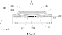
- the height of the welding protrusions 201 refers to the dimension of the welding protrusions 201 in the thickness direction Z of the current collecting member 20, and may also be understood as the thickness of the welding protrusions 201 (shown as H2 in FIG. 12 ).
- the dented depth of the grid structure 111 refers to the maximum dented depth of the grid structure 111 in the thickness direction Z of the current collecting member 20 (shown as H1 in FIG. 12 ).
- the ratio of the height of the welding protrusions 201 to the maximum dented depth of the grid structure 111 is defined to ensure that the welding protrusions 201 have a distance from the grid structure 111 when the welding protrusions 201 are arranged in the avoidance space 113 of the grid structure 111, so that a sufficient avoidance space 113 is reserved for the welding protrusions 201 to reduce the probability of the lower plastic member 11 pressing down against the welding protrusions 201 due to vibrations, so as to reduce the probability of displacement or disalignment of the current collecting member 20 and thus reduce the probability of functional failure of the current collecting member 20, thereby prolonging the service life of the energy storage device 1.
- the ratio of the height of the welding protrusions 201 to the maximum dented depth of the grid structure 111 may be 0.15, 0.2, 0.25, 0.3, 0.35, 0.4, 0.45, 0.5, 0.55, 0.6, 0.65, 0.7, 0.75, 0.8, 0.85, 0.9, 0.95, etc.
- the maximum dented depth of the grid structure 111 is 0.05 mm to 1.8 mm.
- the dented depth of the grid structure 111 refers to the maximum dented depth of the grid structure 111 in the thickness direction Z of the current collecting member 20 (shown as H1 in FIG. 12 ).
- the maximum dented depth of the grid structure 111 is defined to ensure that the grid structure 111 has a sufficient dented depth, so that the welding protrusions 201 have a distance from the grid structure 111 when the welding protrusions 201 are arranged in the avoidance space 113 of the grid structure 111, so that a sufficient avoidance space 113 is reserved for the welding protrusions 201 to reduce the probability of the lower plastic member 11 pressing down against the welding protrusions 201 due to vibrations, so as to reduce the probability of displacement or disalignment of the current collecting member 20 and thus reduce the probability of functional failure of the current collecting member 20, thereby prolonging the service life of the energy storage device 1.
- the maximum dented depth of the grid structure 111 may be 0.05 mm, 0.25 mm, 0.45 mm, 0.65 mm, 0.85 mm, 1.05 mm, 1.25 mm, 1.45 mm, 1.65 mm, 1.75 mm, 1.8 mm, etc.
- This implementation further provides a power consuming apparatus, including an energy storage device according to the above implementation of the disclosure, the energy storage device supplying power to the power consuming apparatus.
- the power consuming apparatus may be applied in the fields of vehicles, power storage stations, etc.
- the illustration is made taking an example in which the power consuming apparatus is a vehicle that may be a fuel vehicle, a gas vehicle or a new energy vehicle.
- the new energy vehicle may be a battery electric vehicle, a hybrid electric vehicle, an extended-range vehicle, etc.
- the vehicle includes a battery, a controller, and a motor.
- the battery is configured to supply power to the controller and the motor as a power source for operating and driving the vehicle.
- the battery is configured to meet the operation power demands during starting, navigation, and traveling of the vehicle.
- the battery supplies power to the controller, the controller controls the battery to supply power to the motor, and the motor receives and uses the power from the battery as a power supply for driving the vehicle, replacing or partially replacing fuel or natural gas to provide driving power for the vehicle.
- the energy storage device In the power consuming apparatus according to this implementation, the energy storage device according to the above implementation of the disclosure is used. Firstly, since in the energy storage device, the vent holes are in communication with the opening by means of the grid structure to allow the vent holes to be in communication with the response member, the vent holes in the grid structure can be used to allow a gas to pass through, so that the response member can be turned over away from the lower plastic member when the predetermined pressure is exceeded. Multiple grids in the grid structure may be further used to prevent the explosion-proof failure due to other components, such as the electrode assembly or the blue film, cracking in some cases and floating to below the response member to block the channel through which the gas passes.
- the grid structure defines the avoidance space, so that the welding protrusions of the current collecting member may be arranged in the avoidance space.
- the lower plastic member has the avoidance space to provide avoidance and receive the welding protrusions of the current collecting member, so that the assembly of the lower plastic member and the current collecting member is more compact, that is, the lower plastic member is attached to the current collecting member more closely, thereby improving the assembly effect of the lower plastic member and the current collecting member.
- the welding protrusions are received in the avoidance space, the welding protrusions are prevented from directly abutting against the second surface of the lower plastic member, so that the overall thickness of the lower plastic member and the current collecting member can be reduced.
- the explosion-proof failure of the energy storage device can be prevented, and the assembly of the lower plastic member and the current collecting member can be more compact, so as to reduce the risk of displacement or disalignment of the current collecting member and thus reduce the risk of failure of the current collecting member.
- the overall thickness of the lower plastic member and the current collecting member can also be reduced.
- example or “implementation” mentioned herein means that a particular feature, structure, or characteristic described with reference to the implementation or implementation may be included in at least one implementation of the disclosure.
- This term appearing in various parts of the specification not necessarily refers to the same implementation, or an independent or alternative implementation that is exclusive to other implementations. Those skilled in the art understand explicitly or implicitly that the implementation described herein may be combined with another implementation.
- the terms “mount”, “connected”, and “connect” should be construed in a broad sense, unless otherwise expressly specified and defined. For example, they may be fixed connection, detachable connection, or integral connection; may be mechanical connection or electrical connection; or may be direct connection, indirect connection by means of an intermediate member, or internal communication between two elements. Those of ordinary skill in the art may understand the meanings of the above terms in the disclosure based on the situation.
Landscapes
- Chemical & Material Sciences (AREA)
- Chemical Kinetics & Catalysis (AREA)
- Electrochemistry (AREA)
- General Chemical & Material Sciences (AREA)
- Cell Electrode Carriers And Collectors (AREA)
- Connection Of Batteries Or Terminals (AREA)
- Sealing Battery Cases Or Jackets (AREA)
Abstract
Description
- The disclosure relates to the technical field of energy storage, and in particular to an energy storage device and a power consuming apparatus.
- In the related art, a current collecting member of an energy storage device is usually arranged on one side of a lower plastic member, and a side of the current collecting member close to the lower plastic member is provided with welding protrusions. Since the welding protrusions protrude from the current collecting member, during assembly or battery transportation, the lower plastic member presses down against the welding protrusions due to vibrations such that the current collecting member moves down to cause a displacement or disalignment of the current collecting member, leading to functional failure of the current collecting member, and thus impairing the service life of the energy storage device.
- In view of this, in a first aspect of the disclosure, an energy storage device with a prolonged service life is provided. The energy storage device includes an electrode assembly, an end cover assembly, and a current collecting member. The end cover assembly includes a top cover, a lower plastic member, and a terminal. The terminal is fixed to the top cover. The top cover includes a response member, the top cover defines an opening, and the response member is attached to the top cover and covers the opening. The lower plastic member is arranged between the top cover and the electrode assembly. The lower plastic member includes a first surface facing the top cover and a second surface facing away from the first surface. The lower plastic member includes a grid structure. The grid structure defines vent holes extending through the grid structure in a thickness direction of the grid structure. The grid structure is arranged opposite the response member in the thickness direction of the energy storage device. The vent holes are in communication with the opening. The current collecting member includes a first connecting portion and a second connecting portion connected to the first connecting portion. The first connecting portion is connected to the terminal, and the second connecting portion is connected to the electrode assembly. A surface of the second connecting portion facing the second surface is provided with welding protrusions, and the second connecting portion at least partially shelters the grid structure. The grid structure defines an avoidance space dented from the second surface towards the first surface, and the welding protrusions is accommodated in the avoidance space.
- A power consuming apparatus is provided in a second aspect of the disclosure. The power consuming apparatus includes the energy storage device provided in the first aspect, the energy storage device is configured to power the power consuming apparatus.
-
- To explain the technical solutions in the implementations of the disclosure more clearly, the accompanying drawings required for the implementations of the disclosure will be described below.
-
FIG. 1 is a perspective schematic structure diagram of an energy storage device according to an implementation of the disclosure. -
FIG. 2 is a perspective schematic structure diagram of the energy storage device shown inFIG. 1 , with a housing removed and then a cell unfolded. -
FIG. 3 is a perspective schematic structure diagram of the energy storage device shown inFIG. 2 from another perspective. -
FIG. 4 is an exploded view of a partial structure of the energy storage device shown inFIG. 2 . -
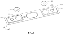
FIG. 5 is an exploded view of structures of a top cover and a response member shown inFIG. 2 . -
FIG. 6 is a schematic cross-sectional diagram of the energy storage device shown inFIG. 2 along line A-A, with the cell removed. -
FIG. 7 is a partial schematic diagram inFIG. 6 . -
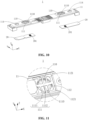
FIG. 8 is a schematic diagram of a lower plastic member fitting with a current collecting member according to an implementation of the disclosure. -
FIG. 9 is an exploded view of the lower plastic member and the current collecting member shown inFIG. 8 . -
FIG. 10 is an exploded view of the lower plastic member and the current collecting member shown inFIG. 8 from another perspective. -
FIG. 11 is a partial schematic diagram inFIG. 9 . -
FIG. 12 is a schematic cross-sectional diagram of the lower plastic member and the current collecting member shown inFIG. 8 along line B-B. - Description of reference numerals:
Energy storage device - 1, end cover assembly - 10, lower plastic member - 11, first surface - 11a, second surface - 11b, through hole - 110, grid structure - 111, vent hole - 1110, first grid - 1111, bent portion - 1111a, supporting portion - 1111b, second grid - 1112, recess - 112, chamfer - 1121, avoidance space - 113, first portion - 113a, second portion - 113b, third portion - 113c, second mounting hole - 114, upper plastic member - 12, top cover - 13, opening - 131, first mounting hole - 132, response member - 14, terminal - 15, current collecting member - 20, welding protrusion - 201, length direction - X, width direction - Y, thickness direction - Z, first connecting portion - 202, second connecting portion - 203, electrode assembly - 30, cell - 40. - Implementations of the disclosure are provided below, and it should be noted that for those of ordinary skill in the art, several improvements and modifications may also be made without departing from the principle of the disclosure, and these improvements and modifications are also considered to be within the scope of protection of the disclosure.
- Referring to
FIGS. 1 to 10 , this implementation provides anenergy storage device 1. Theenergy storage device 1 includes anelectrode assembly 30, anend cover assembly 10, and acurrent collecting member 20. - The
end cover assembly 10 includes atop cover 13, a lowerplastic member 11, and aterminal 15. Theterminal 15 is fixed to thetop cover 13, thetop cover 13 includes aresponse member 14, thetop cover 13 defines anopening 131, and theresponse member 14 is attached to thetop cover 13 and covers theopening 131. The lowerplastic member 11 is arranged between thetop cover 13 and theelectrode assembly 30, the lowerplastic member 11 includes a first surface 11a facing thetop cover 13 and asecond surface 11b facing away from the first surface 11a, the lowerplastic member 11 includes agrid structure 111, thegrid structure 111 definesvent holes 1110 extending through the structure in a thickness direction Z of the grid structure, thegrid structure 111 is arranged opposite theresponse member 14 in the thickness direction Z of theenergy storage device 1, and thevent holes 1110 are in communication with theopening 131. - The current collecting
member 20 is provided. Thecurrent collecting member 20 includes a first connectingportion 202 and a second connectingportion 203 connected to the first connectingportion 202. The first connectingportion 202 is connected to theterminal 15, and the second connectingportion 203 is connected to theelectrode assembly 30. A surface of the second connectingportion 203 facing thesecond surface 11b is provided withwelding protrusions 201, and the second connectingportion 203 at least partially shelters thegrid structure 111. Thegrid structure 111 defines anavoidance space 113 dented from thesecond surface 11b towards the first surface 11a, and thewelding protrusions 201 are accommodated in theavoidance space 113. - It should be noted that the
electrode assembly 30 and the current collectingmember 20, particularly a tab and thecurrent collecting member 20 are welded by an ultrasonic welding process. The current collectingmember 20 and the tab disposed on the current collecting member 20 (collectively referred to as welded parts) are clamped between an upper applicator and a lower applicator, elastic vibration energy generated by ultrasonic waves are input to the welded parts by means of the upper applicator (a welding head of a welding apparatus), the lower applicator (a base of the welding apparatus) supports the welded parts, and contact surfaces of the two welded parts are connected to each other under the actions of a static pressure and high-frequency elastic vibration energy. Therefore, when theelectrode assembly 30 is welded to thecurrent collecting member 20, thewelding protrusions 201 protrude from a surface of thecurrent collecting member 20. - It can be understood that the
energy storage device 1 according to this implementation may include, but is not limited to, a battery cell, a battery module, a battery pack, a battery system, etc. Theenergy storage device 1 may be a square battery when it is a battery cell. - First, it should be noted that the lower
plastic member 11 is a component of a three-dimensional structure with a certain dimension, and thus the lowerplastic member 11 has a length direction, a width direction, and a thickness direction. The length direction may be understood as an X direction in the figures, and the length direction X may also be understood as a direction from one end of the lowerplastic member 11 to the other end of the lowerplastic member 11. The width direction may be understood as a Y direction in the figures, and the width direction Y may also be understood as a direction perpendicular to the direction from one end of the lowerplastic member 11 to the other end of the lowerplastic member 11. The thickness direction may be understood as a Z direction in the figures, and the thickness direction Z may also be understood as a direction in which thetop cover 13, the lowerplastic member 11 and thecurrent collecting member 20 are arranged. In addition, other components such as thecurrent collecting member 20 also have a length direction X, a width direction Y, and a thickness direction Z. The length direction X, the width direction Y and the thickness direction Z of the other components may be understood in the same way as the length direction X, the width direction Y and the thickness direction Z of the lowerplastic member 11, which will not be repeated here in this implementation. - Optionally, the
energy storage device 1 may include a housing, anend cover assembly 10, acurrent collecting member 20, and anelectrode assembly 30. Theend cover assembly 10 includes an upperplastic member 11, a lowerplastic member 12, aterminal 15, atop cover 13, and aresponse member 14. Theelectrode assembly 30 includes a tab and acell 40. Theend cover assembly 10 is mounted inside the housing, and the housing and theend cover assembly 10 enclose a receiving space for receiving thecell 40. For ease of understanding, theelectrode assembly 30 below may also be understood as a tab, and the tab and thecell 40 will be described separately. In this implementation, the technical problems mentioned above can be solved only by using the two structural members, i.e., thelower plastic member 11 and the current collectingmember 20. Next, the structure of theenergy storage device 1 will be described in detail. - As shown in
FIG. 2 , the first surface 11a of thelower plastic member 11 refers to a surface of a side of thelower plastic member 11 facing upwards in the thickness direction Z. Thesecond surface 1 1b of thelower plastic member 11 refers to the surface of the side thelower plastic member 11 facing downwards in the thickness direction Z. - The
top cover 13 is mounted on the first surface 11a of thelower plastic member 11. In other words, thetop cover 13 is arranged on one side of thelower plastic member 11, and thetop cover 13 is arranged on the outer side. Theresponse member 14 may be arranged on thetop cover 13. Specifically, thetop cover 13 defines anopening 131, and theresponse member 14 is mounted in theopening 131 and connected to thetop cover 13. Moreover, the vent holes 1110 of thegrid structure 111 are in communication with theopening 131, such that a gas inside theenergy storage device 1 can enter theopening 131 through the vent holes 1110 and thus impact theresponse member 14. - In other words, the
lower plastic member 11 may define a throughhole 110 facing theresponse member 14. The vent holes 1110 of thegrid structure 111 are in communication with the throughhole 110, and the throughhole 110 is in communication with theopening 131, so as to allow the vent holes 1110 to communicate with theopening 131, such that the gas inside theenergy storage device 1 can enter the throughhole 110 through the vent holes 1110 and then enter theopening 131 through the throughhole 110, and thus impact theresponse member 14. - Optionally, the terminal 15 includes a positive terminal and a negative terminal spaced apart from each other. The
energy storage device 1 further includes metallic electrically-conductive press blocks. The two metallic electrically-conductive press blocks are both arranged on a side of theresponse member 14 facing away from thelower plastic member 11, and the metallic electrically-conductive press blocks are arranged opposite theresponse member 14. One of the metallic electrically-conductive press blocks is connected to the positive terminal, and the other metallic electrically-conductive press block is connected to the negative terminal. - The
electrode assembly 30 includes a positive electrode assembly and a negative electrode assembly. The positive terminal and the positive electrode assembly are both connected to one current collectingmember 20, and the negative terminal and the negative electrode assembly are both connected to another current collectingmember 20. - In this implementation, the
response member 14 is configured to undergo stress deformation in response to an increase in a pressure inside theenergy storage device 1, such that when the gas inside theenergy storage device 1 exceeds a preset pressure threshold, theresponse member 14 can undergo stress deformation and come into contact with the metallic electrically-conductive press block. Therefore, the positive terminal connected to the metallic electrically-conductive press block is externally short-circuited with the negative terminal, and then theresponse member 14 and the bottom of the metallic electrically-conductive press block undergo fusing and topping due to a high short-circuit current to return to an open circuit state, thereby preventing overcharge of theenergy storage device 1 and thus preventing explosion of theenergy storage device 1. - When the
energy storage device 1 encounters an abnormal situation, a large amount of gas will be generated inside theenergy storage device 1 and impact theresponse member 14 through the throughhole 110 in thelower plastic member 11 to turn over theresponse member 14 and thus allow the positive terminal to be connected to the negative terminal of theenergy storage device 1 by means of thetop cover 13. In other words, the positive terminal and the negative terminal are short-circuited to prevent explosion of theenergy storage device 1, thereby effectively protecting theenergy storage device 1. Specifically, when the positive terminal and the negative terminal are short-circuited, the current will not flow in a path from the positive terminal through the current collectingmember 20 and into thecell 40. Instead, the current directly flows from the positive terminal to the negative terminal through thetop cover 13, so as to prevent the current from flowing into thecell 40 and thus prevent the current from causing continued operation of thecell 40 which may aggravate the abnormality. The abnormal situation includes overcharge, over-discharge, violent collision, etc. Under the abnormal situations mentioned above, a large amount of gas will be generated inside theenergy storage device 1 in a short period of time. Alternatively, when theenergy storage device 1 has been used for a long time and theenergy storage device 1 undergoes many charge-discharge cycles, a gas will also be generated inside theenergy storage device 1 and gradually accumulated, such that a large amount of gas will be accumulated inside theenergy storage device 1. In other words, theenergy storage device 1 will bulge after long-term use. - In addition, the
top cover 13 defines a first mountinghole 132, and thelower plastic member 11 defines asecond mounting hole 114 corresponding to the first mountinghole 132. The terminal 15 runs through the first mountinghole 132 and thesecond mounting hole 114, so as to allow the terminal 15 to be mounted to thetop cover 13 and thelower plastic member 11. - Optionally, the
lower plastic member 11 may be made of a material such as plastic by means of injection molding. - In addition, the
lower plastic member 11 may also be provided with agrid structure 111 that is located on a side of the throughhole 110 facing away from theresponse member 14, and thegrid structure 111 is configured to divide a part of the throughhole 110 into multiple vent holes 1110. In other words, thegrid structure 111 divides a part of the throughhole 110 close to the current collectingmember 20 intomultiple vent holes 1110, and eachvent hole 1110 is in communication with the throughhole 110. In other words, the throughhole 110 is located between theresponse member 14 and thegrid structure 111, and thegrid structure 111 is located inside theenergy storage device 1. Thegrid structure 111 is a structure composed of multiple grids. Thegrid structure 111 is not a solid structure, and the multiple grids may surround spaces to define at least onevent hole 1110. Therefore, the vent holes 1110 in thegrid structure 111 may be used to allow the gas to normally enter the throughhole 110, and thus the function of theresponse member 14 will not be affected. Moreover, the multiple grids of thegrid structure 111 may be further used to prevent an explosion-proof failure due to other components, such as theelectrode assembly 30 or a blue film, cracking in some cases and floating to the throughhole 110 below theresponse member 14 to block a channel through which the gas passes. Therefore, thegrid structure 111 can effectively ensure normal service of the function of theresponse member 14. - Optionally, the
grid structure 111 and thelower plastic member 11 may be of an integrated structure or separate structures. When thegrid structure 111 and thelower plastic member 11 are of an integrated structure, thegrid structure 111 and thelower plastic member 11 are both made of plastic. This implementation is only schematically illustrated in the case where thegrid structure 111 and thelower plastic member 11 are of an integrated structure. The specific structures of thegrid structure 111 and thelower plastic member 11 will be described in detail below in this implementation. - In addition, on the basis of the
grid structure 111, in this implementation, the current collectingmember 20 may be arranged on a side of thegrid structure 111 facing away from the throughhole 110. In other words, a portion of the current collectingmember 20 may be located directly below thegrid structure 111. In other words, the portion of the current collectingmember 20 shelters thegrid structure 111; and the other portion of the current collectingmember 20 does not cover thegrid structure 111. - The current collecting
member 20 may abut against thelower plastic member 11 on a periphery of thegrid structure 111, so as to allow the current collectingmember 20 to be mounted to thelower plastic member 11. This is easy for mounting and removal, and since the current collectingmember 20 abuts against thelower plastic member 11, the gas in theenergy storage device 1 can still enter the vent holes 1110 of thegrid structure 111 through a gap between the current collectingmember 20 and thelower plastic member 11 and then enter the throughhole 110. - Optionally, an orthographic projection of the current collecting
member 20 on thetop cover 13 overlaps an orthographic projection of thegrid structure 111 on thetop cover 13. In other words, the current collectingmember 20 can cover at least a part of thegrid structure 111. In other words, the current collectingmember 20 is arranged directly corresponding to at least part of the multiple vent holes 1110. - In this implementation, the current collecting
member 20 is arranged on a side of thegrid structure 111 facing away from theresponse member 14, in other words, the current collectingmember 20 is located directly below thegrid structure 111, and the current collectingmember 20 can cover at least a part of thegrid structure 111. Therefore, thegrid structure 111 can be blocked by the current collectingmember 20, that is, a component made of plastic is blocked by a component made of metal, so as to effectively protect thegrid structure 111 to prevent the grids with thin ribs in thegrid structure 111 from being broken due to factors such as vibrations and bumping during transportation of theenergy storage device 1, thereby improving the stability and the service life of theenergy storage device 1. In addition, the arrangement of the current collectingmember 20 can provide further protection for the throughhole 110, that is, prevent the risk that thebroken electrode assembly 30 is inserted into the current collectingmember 20 and the vent holes 1110 on the periphery of thegrid structure 111, enters the throughhole 110 through the vent holes 1110, and is then short-circuited with theresponse member 14. - The current collecting
member 20 mainly functions as an adapter in theenergy storage device 1, that is, the terminal 15 is indirectly connected to theelectrode assembly 30 by means of the current collectingmember 20. For example, the positive terminal may be indirectly connected to the positive electrode assembly, and the negative terminal may also be indirectly connected to the negative electrode assembly. The current collectingmember 20 is located directly below thegrid structure 111, so that thegrid structure 111 is blocked by the current collectingmember 20, so as to effectively protect thegrid structure 111 to prevent thegrid structure 111 from being broken due to factors such as vibrations or bumping during transportation of theenergy storage device 1, thereby improving the stability and the service life of theenergy storage device 1. Moreover, the arrangement of the current collectingmember 20 can provide further protection for the throughhole 110, that is, prevent the risk that thebroken electrode assembly 30 is inserted into the current collectingmember 20 and the vent holes 1110 on the periphery of and thegrid structure 111, enters the throughholes 110 through thevent hole 1110, and is then short-circuited with theresponse member 14. - Optionally, the material of the current collecting
member 20 includes, but is not limited to, metal, such as copper, aluminum, and nickel. - Optionally, the current collecting
member 20 includes a first connectingportion 202 and a second connectingportion 203. The first connectingportion 202 is located on one side of the second connectingportion 203, and the second connectingportion 203 is provided withwelding protrusions 201 facing thegrid structure 111. - The current collecting
member 20 may include two portions, that is, the first connectingportion 202 and the second connectingportion 203. The first connectingportion 202 is configured to be connected to the terminal 15. The second connectingportion 203 is configured to be connected to theelectrode assembly 30. Specifically, theelectrode assembly 30 may be welded to a surface of a side of the second connectingportion 203 facing away from thelower plastic member 11, so that thewelding protrusions 201 may be formed on a surface of the other side of the second connectingportion 203, that is, the side of the second connectingportion 203 close to thelower plastic member 11. Thewelding protrusions 201 allow theelectrode assembly 30 to be connected to the second connectingportion 203 more closely so as to reduce the probability of pseudo soldering. Optionally, the shapes of thewelding protrusions 201 include, but are not limited to, a diamond, a triangle, a rectangle, and a circle. Optionally, thewelding protrusions 201 are arranged on both the surface of the side of the current collectingmember 20 close to thelower plastic member 11 and the surface of the side of the current collectingmember 20 facing away from thelower plastic member 11. - The terminal 15 runs through from one side of the
lower plastic member 11 to the other side of thelower plastic member 11. Theentire terminal 15 located on one side of thelower plastic member 11 is exposed from theenergy storage device 1, and can be connected to other external components. The terminal 15 running through thelower plastic member 11 to the other side of the lower plastic member is located inside theenergy storage device 1, the surface of the side of the first connectingportion 202 close to thelower plastic member 11 may be electrically connected to the terminal 15 by means of welding, etc., and the surface of the side of the second connectingportion 203 facing away from thelower plastic member 11 may be electrically connected to one end of theelectrode assembly 30 by means of welding, etc. The other end of theelectrode assembly 30 may be connected to thecell 40, so that the terminal 15, the current collectingmember 20, theelectrode assembly 30 and thecell 40 are connected together, which facilitates subsequent current transmission. - Optionally, the current collecting
member 20 further includes a fusing portion arranged between the first connectingportion 202 and the second connectingportion 203, with the width of the fusing portion being less than that of the first connectingportion 202 and that of the second connectingportion 203 in the width direction Y of the current collectingmember 20. - Optionally, the current collecting
member 20 further includes a transition portion arranged between the fusing portion and the second connectingportion 203, and the transition portion defines multiple transition grooves. - Optionally, the fusing portion and/or the transition portion are/is arranged on the current collecting
member 20 corresponding to the positive terminal. In other words, the current collectingmember 20 corresponding to the negative terminal has no fusing portion and no transition portion. - Moreover, the
grid structure 111 defines anavoidance space 113, and theavoidance space 113 is used to accommodate at least part of thewelding protrusions 201. Part of thewelding protrusions 201 is arranged in theavoidance space 113; or all of thewelding protrusions 201 are arranged in theavoidance space 113. For example, a side of thegrid structure 111 close to thewelding protrusions 201 has an avoidance recess; or thegrid structure 111 has an avoidance hole. For example, the side of thegrid structure 111 close to thewelding protrusions 201 protrudes away from thewelding protrusions 201. For another example, theentire grid structure 111 protrudes away from the welding protrusions. - In this implementation, the
grid structure 111 defines theavoidance space 113, so that thewelding protrusions 201 of the current collectingmember 20 may be arranged in theavoidance space 113. In other words, thelower plastic member 11 has theavoidance space 113 to provide avoidance for thewelding protrusions 201 of the current collectingmember 20, so that the assembly of thelower plastic member 11 and the current collectingmember 20 is more compact, that is, thelower plastic member 11 is attached to the current collectingmember 20 more closely, thereby improving the assembly effect of thelower plastic member 11 and the current collectingmember 20. During assembly or battery transportation, since thewelding protrusions 201 may be received in theavoidance space 113, or in other words, thewelding protrusions 201 are located in theavoidance space 113, thewelding protrusions 201 will not directly abut against thelower plastic member 11, which can reduce the probability of thelower plastic member 11 pressing down against thewelding protrusions 201 due to vibrations so as to reduce the probability of the displacement or disalignment of the current collectingmember 20 and thus reduce the probability of functional failure of the current collectingmember 20. - In addition, since the
welding protrusions 201 are received in theavoidance space 113, it is possible to prevent thewelding protrusions 201 from directly abutting against thesecond surface 11b of thelower plastic member 11, so that the overall thickness of thelower plastic member 11 and the current collectingmember 20 can be reduced. - In conclusion, the
energy storage device 1 according to this implementation can not only prevent the explosion-proof failure of theenergy storage device 1, but also improve the stability and the service life of theenergy storage device 1, and allow the assembly of thelower plastic member 11 and the current collectingmember 20 to be more compact, so as to reduce the risk of displacement or disalignment of the current collectingmember 20 and thus reduce the risk of failure of the current collectingmember 20. In addition, theenergy storage device 1 according to this implementation may further reduce the overall thickness of thelower plastic member 11 and the current collectingmember 20. - Referring to
FIGS. 5 to 10 , optionally, in this implementation, the surface of the side of thegrid structure 111 close to the current collectingmember 20 is bent and dented away from the current collectingmember 20 to define theavoidance space 113. - In an implementation, the grids of the
grid structure 111 may be bent away from the current collectingmember 20, so that the grids are bent and dented away from the current collectingmember 20 as a whole to define theavoidance space 113 mentioned above, so that the difficulty of manufacturing thegrid structure 111 can be reduced. Since the surface of the other side of the grid corresponds to the throughhole 110, the normal use of theresponse member 14 will not be affected when the surface of the other side of the grid protrudes or even enters the throughhole 110. - In another implementation, the surface of the side of the grid close to the current collecting
member 20 in thegrid structure 111 can be bent and dented, so that the surface of the side of the grid close to the current collectingmember 20 is bent and dented away from the current collectingmember 20 to define theavoidance space 113. For example, the surface of the side of the grid close to the current collectingmember 20 is slotted to define theavoidance space 113 mentioned above. - Referring to
FIGS. 6 and7 , in this implementation, theavoidance space 113 has afirst portion 113a, a second portion 113b, and a third portion 113c. The second portion 113b is connected between thefirst portion 113a and the third portion 113c, a dented depth of thefirst portion 113a and a dented depth of the third portion 113c are both less than a dented depth of the second portion 113b, and at least part of thewelding protrusions 201 faces the second portion 113b in the thickness direction Z of theenergy storage device 1. - The
avoidance space 113 may include three regions, that is, afirst portion 113a, a second portion 113b, and a third portion 113c. The second portion 113b is arranged between thefirst portion 113a and the third portion 113c, so that the second portion 113b may also be understood as a central region of theavoidance space 113, and thefirst portion 113a and the third portion 113c may be understood as peripheral regions of theavoidance space 113. Moreover, the dented depth of thefirst portion 113a and the dented depth of the third portion 113c are both less than that of the second portion 113b. In other words, the dented depth of the central region of theavoidance space 113 is greater than those of the peripheral regions of theavoidance space 113, that is, theavoidance space 113 is a depression that is shallow at its edge and deep in the middle. Optionally, thefirst portion 113a and the third portion 113c are arranged symmetrically. The dented depth of thefirst portion 113a is equal to that of the third portion 113c. - At least part of the
welding protrusions 201 faces the second portion 113b in the thickness direction Z of theenergy storage device 1, and it can also be understood that thewelding protrusions 201 are arranged directly corresponding to the second portion 113b. Thewelding protrusions 201 are arranged in the second portion 113b with a greater dented depth, so as to providemore avoidance space 113 for thewelding protrusions 201 to reduce the probability of thewelding protrusions 201 coming into contact with thelower plastic member 11, so that the assembly of thelower plastic member 11 and the current collectingmember 20 is more compact. Optionally, a height of each of thewelding protrusions 201 is less than the dented depth of the second portion 113b and greater than the dented depth of thefirst portion 113a and the dented depth of the third portion 113c. In this implementation, since the height of thewelding protrusions 201 is greater than the dented depth of thefirst portion 113a and the dented depth of the third portion 113c, the grids of thefirst portion 113a and the third portion 113c can limit the position of thewelding protrusions 201 of the current collectingmember 20 on thelower plastic member 11, and also reduce the probability of thelower plastic member 11 pressing down against thewelding protrusions 201 due to vibrations, so as to reduce the probability of displacement or disalignment of the current collectingmember 20 and thus reduce the probability of functional failure of the current collectingmember 20. In addition, the grids of thefirst portion 113a and the third portion 113c can fit with the grids of the second portion 113b, so as to provide a positioning function during assembly of thelower plastic member 11 and the current collectingmember 20, thereby reducing the assembly difficulty. - Optionally, the
welding protrusions 201 are divided into a fourth part, a fifth part, and a sixth part. The fifth part is arranged between the fourth part and the sixth part, and the height of each welding protrusion in the fourth part and the height of each welding protrusion in the sixth part are both less than that of each welding protrusion in the fifth part. Thewelding protrusions 201 of the fourth part face theavoidance space 113 of thefirst portion 113a, thewelding protrusions 201 of the fifth part face theavoidance space 113 of the second portion 113b, and thewelding protrusions 201 of the sixth part face theavoidance space 113 of the third portion 113c. - Referring to
FIGS. 9 and11 , in this implementation, thegrid structure 111 includes multiplefirst grids 1111 arranged at intervals in a length direction of thelower plastic member 11; every adjacent two of thefirst grids 1111 surround a space to define avent hole 1110; and at least part of each of thefirst grids 1111 is bent away from the current collectingmember 20 to define theavoidance space 113. - The
grid structure 111 may include multiplefirst grids 1111 configured to surround spaces to define multiple vent holes 1110. Thefirst grids 1111 and thelower plastic member 11 form an integrally formed structural member. There are 2-6first grids 1111. Every two adjacentfirst grids 1111 are equally spaced. For example, thegrid structure 111 includes threefirst grids 1111 arranged at intervals in the length direction X of the current collectingmember 20, and the two adjacentfirst grids 1111 may surround spaces to two vent holes 1110. Thefirst grids 1111 together with a partial structure of thelower plastic member 11 may also define two further vent holes 1110 . Optionally, twovent holes 1110 of the fourvent holes 1110 in the middle protrude from the current collectingmember 20. Further, optionally, all the fourvent holes 1110 protrude from the current collectingmember 20. - At least part of each of the
first grids 1111 is at least partially bent away from the current collectingmember 20 to define theavoidance space 113. Optionally, in an implementation, a part of each of thefirst grids 1111 is bent away from the current collectingmember 20 to define theavoidance space 113. In another implementation, middle portions of thefirst grids 1111 are bent away from the current collectingmember 20 to define theavoidance space 113. In yet another implementation, the entireties of thefirst grids 1111 are bent away from the current collectingmember 20 to define theavoidance space 113. - In this implementation, by means of arranging the multiple
first grids 1111 and allowing at least part of each of thefirst grids 1111 to be bent, thelower plastic member 11 has theavoidance space 113 to provide avoidance for thewelding protrusions 201 of the current collectingmember 20. In this way, thegrid structure 111 defines theavoidance space 113 to allow thewelding protrusions 201 to be arranged in theavoidance space 113, so that thelower plastic member 11 is attached to the current collectingmember 20 more closely, and the overall thickness is reduced; and thegrid structure 111 hasmultiple vent holes 1110 to allow gas to normally enter the throughhole 110, and the multiplefirst grids 1111 may also be used to prevent the explosion-proof failure due to other components, such as theelectrode assembly 30 or the blue film, cracking in some cases and floating to the throughhole 110 below theresponse member 14 to block the channel through which the gas passes. - Referring to
FIGS. 8, 9 ,11 and12 , in this implementation, thefirst grid 1111 includes abent portion 111 1a and supportingportions 111 1b arranged on two opposite sides of thebent portion 111 1a, and thebent portion 1111a is bent away from the current collectingmember 20 to form theavoidance space 113. - The
first grid 1111 may include a supportingportion 1111b and abent portion 1111a. The supportingportion 1111b is configured to support thebent portion 1111a and/or the current collectingmember 20, and thebent portion 1111a is configured to form theavoidance space 113. The surface of the side of the supportingportion 1111b close to the current collectingmember 20 is arranged horizontally to the surface of the side of thelower plastic member 11 close to the current collectingmember 20. Optionally, the supportingportion 1111b and thebent portion 1111a form an integrally formed structural member. The supportingportion 1111b, thebent portion 1111a and thelower plastic member 11 form an integrally formed structural member. - In this implementation, the supporting
portion 1111b and thebent portion 1111a are provided and fit with each other, so that thebent portion 1111a can form theavoidance space 113, and thewelding protrusions 201 can be arranged in theavoidance space 113, so that thelower plastic member 11 is attached to the current collectingmember 20 more closely, so as to reduce the risk of displacement or disalignment of the current collectingmember 20 and thus reduce the risk of failure of the current collectingmember 20. In addition, in theenergy storage device 1 of this implementation, the overall thickness of thelower plastic member 11 and the current collectingmember 20 may also be reduced. In this implementation, the supportingportion 111 1b can support thebent portion 1111a and/or the current collectingmember 20, so as to improve the supporting capacity of thegrid structure 111, thereby improving the stability of theenergy storage device 1. - Referring to
FIGS. 11 and12 , in this implementation, thesecond surface 11b of thelower plastic member 11 defines arecess 112, thegrid structure 111 is arranged in therecess 112, the first surface 11a of thelower plastic member 11 defines a throughhole 110, the throughhole 110 runs through thesecond surface 11b of thelower plastic member 11 and a bottom wall of therecess 112, thefirst grids 1111 may also enclose the vent holes 1110 with a side wall of therecess 112, the supportingportion 1111b is arranged opposite the bottom wall of therecess 112, and thebent portion 1111a is arranged opposite the throughhole 110. - The
lower plastic member 11 may define arecess 112, thegrid structure 111 is arranged in therecess 112, and the throughhole 110 runs through a bottom wall of therecess 112, so that the throughhole 110 can be in communication with thegrid structure 111, and the overall thickness of thelower plastic member 11 can also be reduced. - The
first grids 1111 may also enclosevent holes 1110 with a side wall of therecess 112, and thefirst grids 1111 are arranged on the side wall of therecess 112. Optionally, in an implementation, thefirst grid 1111 is arranged on the side wall of therecess 112, and there is a gap between thefirst grid 1111 and the bottom wall of therecess 112. In another implementation, thefirst grid 1111 may be arranged on both the bottom wall and the side wall of therecess 112. This implementation is only schematically illustrated in the case where thefirst grid 1111 is arranged on both the bottom wall and the side wall of therecess 112. - Optionally, in an implementation, the supporting
portion 1111b is arranged on the side wall of therecess 112, and there is a gap between the supportingportion 1111b and the bottom wall of therecess 112. In another implementation, the supportingportion 1111b is arranged on both the bottom wall and the side wall of therecess 112. Optionally, thebent portion 1111a is at least partially arranged in the throughhole 110. - The supporting
portion 111 1b is arranged opposite the bottom wall of therecess 112, which may also be understood as that the supportingportion 1111b is arranged directly corresponding to the bottom wall of therecess 112. In other words, the orthographic projection of the supportingportion 111 1b on the side of thelower plastic member 11 close to the current collectingmember 20 is located in the bottom wall of therecess 112. In other words, the supportingportion 1111b is arranged on the bottom wall and/or the side wall of therecess 112. This arrangement can allow thefirst grid 1111 to be attached to therecess 112 of thelower plastic member 11 more closely, and enhance the overall strength of thegrid structure 111, thereby improving the overall stability of thegrid structure 111. In addition, thebent portion 1111a is arranged opposite the throughhole 110, which may also be understood as that thebent portion 1111a is arranged directly corresponding to the throughhole 110. This arrangement may provide more space that thebent portion 1111a is dented away from the current collectingmember 20, that is, provide alarger avoidance space 113. - Optionally, in an implementation, the
grid structure 111 may be arranged on the bottom wall of therecess 112. In another implementation, thegrid structure 111 may be arranged on the side wall of therecess 112. In yet another implementation, thegrid structure 111 may be arranged on both the bottom wall and the side wall of therecess 112. - Referring to
FIG. 11 , in this implementation, thetop cover 13 defines a first mountinghole 132, thelower plastic member 11 defines asecond mounting hole 114 arranged opposite the first mountinghole 132, thesecond mounting hole 114 runs through the first surface 11a and thesecond surface 11b, the terminal 15 runs through the first mountinghole 132 and thesecond mounting hole 114, the side wall of therecess 112 away from thesecond mounting hole 114 has twochamfers 1121 arranged opposite each other in the width direction Y of thelower plastic member 11, and the end of the second connectingportion 203 away from the first connectingportion 202 is arranged opposite the twochamfers 1121. - The end of the second connecting
portion 203 away from the first connectingportion 202 is arranged opposite the twochamfers 1121, in other words, the second connectingportion 203 abuts against thechamfers 1121 of the side wall of therecess 112, or the second connectingportion 203 is clamped at thechamfers 1121 of the side wall of therecess 112. In this implementation, the side wall of therecess 112 away from thesecond mounting hole 114 is provided with the twochamfers 1121, and the twochamfers 1121 are configured to correspond to the end of the second connectingportion 203 away from the first connectingportion 202, so that the current collectingmember 20 can be reliably lapped on the side wall of therecess 112, and thus the current collectingmember 20 does not need to be lapped on thesecond surface 11b outside therecess 112 of thelower plastic member 11 away from thesecond mounting hole 114, so that the length of the current collectingmember 20 is effectively limited to avoid waste of materials in the case that the current collectingmember 20 is too long. Moreover, the position of the current collectingmember 20 can be further limited by clamping the current collectingmember 20 by means of thechamfers 1121, so as to prevent thegrid structure 111 from being damaged by vibration when thewelding protrusions 201 come into direct contact with thegrid structure 111. - Referring to
FIGS. 8 and12 , in this implementation, the supportingportion 1111b at least partially abuts against the second connectingportion 203 of the current collectingmember 20. - Optionally, in an implementation, a portion of the supporting
portion 1111b may abut against the second connectingportion 203 of the current collectingmember 20. In another implementation, the whole supportingportion 1111b may abut against the second connectingportion 203 of the current collectingmember 20. This implementation is only schematically illustrated in the case where a portion of the supportingportion 111 1b abuts against the second connectingportion 203 of the current collectingmember 20. - In this implementation, the second connecting
portion 203 of the current collectingmember 20 may abut against at least a part of the supportingportion 1111b, so that thebent portion 1111a is located directly above the current collectingmember 20. This can effectively protect thebent portion 1111a of thegrid structure 111 to prevent theavoidance space 113 from being destroyed during transportation of theenergy storage device 1 caused by thegrid structure 111 being broken due to factors such as vibration or bumping or caused by the deformation of thebent portion 111 1a, thereby improving the stability and prolonging the service life of theenergy storage device 1. - Referring to
FIG. 11 , in this implementation, thegrid structure 111 further includes asecond grid 1112 extending in the same direction as the length direction X of thelower plastic member 11, thesecond grid 1112 is connected to the multiplefirst grids 1111, the two opposite ends of thesecond grid 1112 are both connected to the side wall of therecess 112, and thesecond grid 1112 is entirely bent away from the current collectingmember 20 to form theavoidance space 113. - Referring to
FIG. 7 , in this implementation, thetop cover 13 defines a first mountinghole 132, thelower plastic member 11 defines asecond mounting hole 114 corresponding to the first mountinghole 132, thesecond mounting hole 114 extends through the first surface 11a and thesecond surface 11b, the terminal 15 extends through the first mountinghole 132 and thesecond mounting hole 114, and in the length direction X of thelower plastic member 11, the one end of the second connectingportion 203 away from the first connectingportion 202 goes beyond one end of thesecond grid 1112 away from thesecond mounting hole 114. - The end of the second connecting
portion 203 away from the first connectingportion 202 abuts against thesecond surface 11b of thelower plastic member 11 on the side of thesecond grid 1112 away from thesecond mounting hole 114. In other words, the end of the second connectingportion 203 away from the first connectingportion 202 goes beyond the end of thesecond grid 1112 away from thesecond mounting hole 114. It can also be understood that the rightmost end of the current collectingmember 20 can be reliably lapped on the rightmostsecond surface 11b of thesecond grid 1112. - In this implementation, limiting the position of the end of the second connecting
portion 203 away from the first connectingportion 202 can ensure that the second connectingportion 203 of the current collectingmember 20 can be reliably lapped on thesecond surface 11b of thelower plastic member 11 on the side of thesecond grid 1112 away from thesecond mounting hole 114. Moreover, since the current collectingmember 20 is relatively protruding, or in other words, the current collectingmember 20 is relatively long, it is also possible to provide a certain error tolerance for a position where the current collectingmember 20 is welded to the terminal 15 (that is, the lapping at the rightmost end can be achieved in case of welding a little to the left or to the right), in other words, it is also possible to provide a certain error tolerance for the first connectingportion 202. - Referring to
FIG. 7 , in this implementation, the end of the second connectingportion 203 away from the first connectingportion 202 goes beyond the end of thesecond grid 1112 away from thesecond mounting hole 114 by a distance of 1 mm to 12 mm. - In this implementation, the end of the second connecting
portion 203 away from the first connectingportion 202 goes beyond the end of thesecond grid 1112 away from thesecond mounting hole 114 by a distance (shown as L inFIG. 7 ) of 1 mm to 12 mm. This can ensure that the second connectingportion 203 of the current collectingmember 20 can be reliably lapped on thesecond surface 1 1b of thesecond grid 1112 on the side away from thesecond mounting hole 114 in thelower plastic member 11, and can also provide a certain error tolerance for the position where the current collectingmember 20 is welded to the terminal 15 (that is, the lapping at the rightmost end can be achieved in case of welding a little to the left or to the right), in other words, it is also possible to provide a certain error tolerance for the first connectingportion 202. - Optionally, the end of the second connecting
portion 203 away from the first connectingportion 202 goes beyond the end of thesecond grid 1112 away from thesecond mounting hole 114 by a distance of 1 mm, 2 mm, 3 mm, 4 mm, 5 mm, 6 mm, 7 mm, 8 mm, 9 mm, 10 mm, 11 mm, 12 mm, etc. - The
grid structure 111 may further include asecond grid 1112. Optionally, thesecond grid 1112 extends in the same direction as the length direction X of thelower plastic member 11. Thesecond grid 1112 is arranged perpendicular to thefirst grids 1111. Thefirst grids 1111 and thesecond grid 1112 form an integrally formed structural member. Thefirst grids 1111, thesecond grid 1112 and thelower plastic member 11 form an integrally formed structural member. Thesecond grid 1112 has a width greater than that of thefirst grids 1111. Thesecond grid 1112, thefirst grids 1111, and a side wall of therecess 112 surround spaces to define multiple vent holes 1110. In the width direction Y of the current collectingmember 20, thesecond grid 1112 has the same distance from side walls of two opposite sides of therecess 112. - In this implementation, the
second grid 1112 has two ends respectively connected to the side walls of therecess 112, and thesecond grid 1112 extends through thefirst grids 1111, so that thegrid structure 111 is fixed and has an enhanced overall strength so as to prevent thegrid structure 111 from being broken due to factors such as vibrations or bumping during transportation of theenergy storage device 1, thereby improving the stability and the service life of theenergy storage device 1. - Referring to
FIGS. 8 and12 , in this implementation, the supportingportion 1111b is flush with a surface of thelower plastic member 11 that defines therecess 112. This can improve the flatness of the surface of thelower plastic member 11 and reduce the difficulty of machining and molding. Moreover, the assembly of the current collectingmember 20 with thegrid structure 111 and thelower plastic member 11 is more compact, that is, the supportingportion 111 1b is flush with the surface of thelower plastic member 11 that defines therecess 112, so that both the supportingportion 1111b and the surface of thelower plastic member 11 that defines therecess 112 can abut against the current collectingmember 20. In other words, the current collectingmember 20 can not only abut against the surface of thelower plastic member 11 that defines therecess 112, but also abut against the supportingportion 1111b of thegrid structure 111, so that the assembly of thelower plastic member 11 and the current collectingmember 20 is more compact, so as to reduce the probability of displacement or disalignment of the current collectingmember 20 and thus reduce the probability of functional failure of the current collectingmember 20. - Referring to
FIG. 12 , in this implementation, a ratio of a height of thewelding protrusions 201 to the maximum dented depth of thegrid structure 111 is 0.15-0.95. - The height of the
welding protrusions 201 refers to the dimension of thewelding protrusions 201 in the thickness direction Z of the current collectingmember 20, and may also be understood as the thickness of the welding protrusions 201 (shown as H2 inFIG. 12 ). The dented depth of thegrid structure 111 refers to the maximum dented depth of thegrid structure 111 in the thickness direction Z of the current collecting member 20 (shown as H1 inFIG. 12 ). - In this implementation, the ratio of the height of the
welding protrusions 201 to the maximum dented depth of thegrid structure 111 is defined to ensure that thewelding protrusions 201 have a distance from thegrid structure 111 when thewelding protrusions 201 are arranged in theavoidance space 113 of thegrid structure 111, so that asufficient avoidance space 113 is reserved for thewelding protrusions 201 to reduce the probability of thelower plastic member 11 pressing down against thewelding protrusions 201 due to vibrations, so as to reduce the probability of displacement or disalignment of the current collectingmember 20 and thus reduce the probability of functional failure of the current collectingmember 20, thereby prolonging the service life of theenergy storage device 1. - Optionally, the ratio of the height of the
welding protrusions 201 to the maximum dented depth of thegrid structure 111 may be 0.15, 0.2, 0.25, 0.3, 0.35, 0.4, 0.45, 0.5, 0.55, 0.6, 0.65, 0.7, 0.75, 0.8, 0.85, 0.9, 0.95, etc. - Referring to
FIG. 12 , in this implementation, the maximum dented depth of thegrid structure 111 is 0.05 mm to 1.8 mm. - The dented depth of the
grid structure 111 refers to the maximum dented depth of thegrid structure 111 in the thickness direction Z of the current collecting member 20 (shown as H1 inFIG. 12 ). - In this implementation, the maximum dented depth of the
grid structure 111 is defined to ensure that thegrid structure 111 has a sufficient dented depth, so that thewelding protrusions 201 have a distance from thegrid structure 111 when thewelding protrusions 201 are arranged in theavoidance space 113 of thegrid structure 111, so that asufficient avoidance space 113 is reserved for thewelding protrusions 201 to reduce the probability of thelower plastic member 11 pressing down against thewelding protrusions 201 due to vibrations, so as to reduce the probability of displacement or disalignment of the current collectingmember 20 and thus reduce the probability of functional failure of the current collectingmember 20, thereby prolonging the service life of theenergy storage device 1. - Optionally, the maximum dented depth of the
grid structure 111 may be 0.05 mm, 0.25 mm, 0.45 mm, 0.65 mm, 0.85 mm, 1.05 mm, 1.25 mm, 1.45 mm, 1.65 mm, 1.75 mm, 1.8 mm, etc. - This implementation further provides a power consuming apparatus, including an energy storage device according to the above implementation of the disclosure, the energy storage device supplying power to the power consuming apparatus.
- The power consuming apparatus according to this implementation may be applied in the fields of vehicles, power storage stations, etc. Optionally, the illustration is made taking an example in which the power consuming apparatus is a vehicle that may be a fuel vehicle, a gas vehicle or a new energy vehicle. The new energy vehicle may be a battery electric vehicle, a hybrid electric vehicle, an extended-range vehicle, etc. The vehicle includes a battery, a controller, and a motor. The battery is configured to supply power to the controller and the motor as a power source for operating and driving the vehicle. For example, the battery is configured to meet the operation power demands during starting, navigation, and traveling of the vehicle. For example, the battery supplies power to the controller, the controller controls the battery to supply power to the motor, and the motor receives and uses the power from the battery as a power supply for driving the vehicle, replacing or partially replacing fuel or natural gas to provide driving power for the vehicle.
- In the power consuming apparatus according to this implementation, the energy storage device according to the above implementation of the disclosure is used. Firstly, since in the energy storage device, the vent holes are in communication with the opening by means of the grid structure to allow the vent holes to be in communication with the response member, the vent holes in the grid structure can be used to allow a gas to pass through, so that the response member can be turned over away from the lower plastic member when the predetermined pressure is exceeded. Multiple grids in the grid structure may be further used to prevent the explosion-proof failure due to other components, such as the electrode assembly or the blue film, cracking in some cases and floating to below the response member to block the channel through which the gas passes.
- Secondly, the grid structure defines the avoidance space, so that the welding protrusions of the current collecting member may be arranged in the avoidance space. In other words, the lower plastic member has the avoidance space to provide avoidance and receive the welding protrusions of the current collecting member, so that the assembly of the lower plastic member and the current collecting member is more compact, that is, the lower plastic member is attached to the current collecting member more closely, thereby improving the assembly effect of the lower plastic member and the current collecting member. During assembly or battery transportation, since the welding protrusions may be received in the avoidance space, it is possible to reduce the probability of the lower plastic member pressing down against the welding protrusions due to vibration, so as to reduce the probability of displacement or disalignment of the current collecting member and thus reduce the probability of functional failure of the current collecting member.
- In addition, since the welding protrusions are received in the avoidance space, the welding protrusions are prevented from directly abutting against the second surface of the lower plastic member, so that the overall thickness of the lower plastic member and the current collecting member can be reduced.
- In conclusion, in the power consuming apparatus according to this implementation, using the above energy storage device, the explosion-proof failure of the energy storage device can be prevented, and the assembly of the lower plastic member and the current collecting member can be more compact, so as to reduce the risk of displacement or disalignment of the current collecting member and thus reduce the risk of failure of the current collecting member. In addition, according to the energy storage device of the disclosure, the overall thickness of the lower plastic member and the current collecting member can also be reduced.
- The "example" or "implementation" mentioned herein means that a particular feature, structure, or characteristic described with reference to the implementation or implementation may be included in at least one implementation of the disclosure. This term appearing in various parts of the specification not necessarily refers to the same implementation, or an independent or alternative implementation that is exclusive to other implementations. Those skilled in the art understand explicitly or implicitly that the implementation described herein may be combined with another implementation.
- It should be noted that the terms "first", "second", and the like in the specification, the claims, and the accompanying drawings of the disclosure are used to distinguish different objects, rather than to describe a particular order. In addition, the terms "include" and "have" and any variations thereof are intended to cover a non-exclusive inclusion.
- In this specification, for the sake of convenience, the expressions indicating an orientation or positional relationship such as "middle", "upper", "lower", "front", "rear", "vertical", "horizontal", "top", "bottom", "inner" and "outer" are intended to illustrate the positional relationship between the constituent elements with reference to the accompanying drawings, and are merely for ease of description of this specification and simplification of the description, rather than indicating or implying that the device or elements referred to must have a specific orientation or be constructed and operated in a specific orientation, and therefore cannot be construed as limiting the disclosure. The position relationship between the constituent elements is appropriately changed depending on directions of the described constituent elements. Therefore, the position relationship is not limited to the words described in the specification, which may be appropriately replaced depending on the situation.
- In this specification, the terms "mount", "connected", and "connect" should be construed in a broad sense, unless otherwise expressly specified and defined. For example, they may be fixed connection, detachable connection, or integral connection; may be mechanical connection or electrical connection; or may be direct connection, indirect connection by means of an intermediate member, or internal communication between two elements. Those of ordinary skill in the art may understand the meanings of the above terms in the disclosure based on the situation.
Claims (14)
- An energy storage device (1), comprising:an electrode assembly (30);an end cover assembly (10), the end cover assembly (10) comprising a top cover (13), a lower plastic member (11), and a terminal (15), wherein the terminal (15) is fixed to the top cover (13), the top cover (13) comprises a response member (14), the top cover (13) defines an opening (131), and the response member (14) is attached to the top cover (13) and covers the opening (131); and the lower plastic member (11) is arranged between the top cover (13) and the electrode assembly (30), the lower plastic member (11) comprises a first surface (11a) facing the top cover (13) and a second surface (11b) facing away from the first surface (11a), the lower plastic member (11) comprises a grid structure (111), the grid structure (111) defines vent holes (1110) extending through the grid structure (111) in a thickness direction (Z) of the grid structure (111), the grid structure (111) is arranged opposite the response member (14) in the thickness direction (Z) of the energy storage device (1), and the vent holes (1110) are in communication with the opening (131); anda current collecting member (20), the current collecting member (20) comprising a first connecting portion (202) and a second connecting portion (203) connected to the first connecting portion (202), wherein the first connecting portion (202) is connected to the terminal (15), and the second connecting portion (203) is connected to the electrode assembly (30); a surface of the second connecting portion (203) facing the second surface (11b) is provided with welding protrusions (201), and the second connecting portion (203) at least partially shelters the grid structure (111); and the grid structure (111) defines an avoidance space (113) dented from the second surface (11b) towards the first surface (11a), and the welding protrusions (201) is accommodated in the avoidance space (113);the avoidance space (113) has a first portion (113a), a second portion (113b), and a third portion (113c), the second portion (113b) is connected between the first portion (113a) and the third portion (113c), a dented depth of the first portion (1 13a) and a dented depth of the third portion (113c) are both less than a dented depth of the second portion (1 13b), at least part of the welding protrusions (201) faces the second portion (113b) in the thickness direction (Z) of the energy storage device (1), a height of each of the welding protrusions (201) is less than the dented depth of the second portion (113b) and greater than each of the dented depth of the first portion (113a) and the dented depth of the third portion (113c).
- The energy storage device (1) according to claim 1, wherein the grid structure (111) comprises a plurality of first grids (1111) arranged at intervals in a length direction (X) of the lower plastic member (11); every adjacent two of the first grids (1111) surround a space to define the vent hole (1110); and at least part of each of the first grids (1111) is bent away from the current collecting member (20) to define the avoidance space (113).
- The energy storage device (1) according to claim 2, wherein each of the plurality of first grids (1111) comprises a bent portion (1111a) and supporting portions (111 1b) arranged on two opposite sides of the bent portion (1111a), and the bent portion (1111a) is bent away from the current collecting member (20) to form the avoidance space (113).
- The energy storage device (1) according to claim 3, wherein the second surface (11b) of the lower plastic member (11) defines a recess (112), the grid structure (111) is arranged in the recess (112), the first surface (11a) of the lower plastic member (11) defines a through hole (110), the through hole (110) extends through the second surface (11b) of the lower plastic member (11) and a bottom wall of the recess (112), the first grids (1111) and side walls of the recess (112) cooperatively define spaces as the vent holes (1110), the supporting portion (1 1 1 1b) faces the bottom wall of the recess (112), and the bent portion (111 1a) faces the through hole (110).
- The energy storage device (1) according to claim 4, wherein the top cover (13) defines a first mounting hole (132), the lower plastic member (11) defines a second mounting hole (114) corresponding to the first mounting hole (132), the second mounting hole (114) extends through the first surface (11a) and the second surface (11b), the terminal (15) extends through the first mounting hole (132) and the second mounting hole (114), the side walls of the recess (112) away from the second mounting hole (114) have two chamfers (1121) arranged opposite each other in a width direction (Y) of the lower plastic member (11), and one end of the second connecting portion (203) away from the first connecting portion (202) faces the two chamfers (1121).
- The energy storage device (1) according to claim 4 or 5, wherein at least part of the supporting portion (1111b) abuts against the second connecting portion (203) of the current collecting member (20).
- The energy storage device (1) according to any one of claims 4 to 6, wherein the grid structure (111) further comprises a second grid (1112) extending in the same direction as the length direction (X) of the lower plastic member (11), the second grid (1112) is connected to the plurality of first grids (1111), two opposite ends of the second grid (1112) are both connected to the side walls of the recess (112), and the second grid (1112) is entirely bent away from the current collecting member (20) to define the avoidance space (113).
- The energy storage device (1) according to claim 7, wherein the top cover (13) defines a first mounting hole (132), the lower plastic member (11) defines a second mounting hole (114) corresponding to the first mounting hole (132), the second mounting hole (114) extends through the first surface (11a) and the second surface (11b), the terminal (15) extends through the first mounting hole (132) and the second mounting hole (114), and in the length direction (X) of the lower plastic member (11), the one end of the second connecting portion (203) away from the first connecting portion (202) goes beyond one end of the second grid (1112) away from the second mounting hole (114).
- The energy storage device (1) according to claim 8, wherein the one end of the second connecting portion (203) away from the first connecting portion (202) goes beyond the one end of the second grid (1112) away from the second mounting hole (114) by a distance of 1 mm to 12 mm.
- The energy storage device (1) according to any one of claims 4 to 9, wherein the supporting portion (1111b) is flush with the second surface (11b) of the lower plastic member (11) that defines the recess (112).
- The energy storage device (1) according to any one of claims 1 to 10, wherein an orthographic projection of the current collecting member (20) on the top cover (13) overlaps an orthographic projection of the grid structure (111) on the top cover (13).
- The energy storage device (1) according to any one of claims 1 to 11, wherein a ratio of a height of the welding protrusions (201) to the maximum dented depth of the grid structure (111) is 0.15-0.95.
- The energy storage device (1) according to claim 12, wherein the maximum dented depth of the grid structure (111) is 0.05 mm to 1.8 mm.
- A power consuming apparatus, comprising the energy storage device (1) according to any one of claims 1 to 13, the energy storage device (1) being configured to power the power consuming apparatus.
Applications Claiming Priority (1)
| Application Number | Priority Date | Filing Date | Title |
|---|---|---|---|
| CN202310091066.5A CN116014319B (en) | 2023-02-09 | 2023-02-09 | Energy storage device and electrical equipment |
Publications (2)
| Publication Number | Publication Date |
|---|---|
| EP4415128A1 true EP4415128A1 (en) | 2024-08-14 |
| EP4415128B1 EP4415128B1 (en) | 2025-05-21 |
Family
ID=86029950
Family Applications (1)
| Application Number | Title | Priority Date | Filing Date |
|---|---|---|---|
| EP23212544.3A Active EP4415128B1 (en) | 2023-02-09 | 2023-11-28 | Energy storage device and power consuming apparatus |
Country Status (4)
| Country | Link |
|---|---|
| US (1) | US12119504B2 (en) |
| EP (1) | EP4415128B1 (en) |
| CN (1) | CN116014319B (en) |
| HU (1) | HUE072569T2 (en) |
Families Citing this family (4)
| Publication number | Priority date | Publication date | Assignee | Title |
|---|---|---|---|---|
| CN115882171B (en) * | 2023-02-09 | 2023-05-16 | 深圳海润新能源科技有限公司 | Energy storage device and electric equipment |
| CN116387711B (en) * | 2023-05-31 | 2023-08-11 | 深圳海辰储能控制技术有限公司 | Lower plastic, end cover components, energy storage devices and electrical equipment |
| CN116780127A (en) * | 2023-08-16 | 2023-09-19 | 深圳海辰储能控制技术有限公司 | Lower plastic, end cover components, energy storage device and electrical equipment |
| CN121238103A (en) * | 2024-06-28 | 2025-12-30 | 宁德时代新能源科技股份有限公司 | Battery cells, batteries and electrical devices |
Citations (4)
| Publication number | Priority date | Publication date | Assignee | Title |
|---|---|---|---|---|
| CN213026283U (en) * | 2020-10-21 | 2021-04-20 | 昆山聚创新能源科技有限公司 | Battery cover and battery |
| CN215418346U (en) * | 2021-04-12 | 2022-01-04 | 江苏正力新能电池技术有限公司 | Plastic structure of power battery top cap, top cap and battery |
| CN215988965U (en) * | 2021-09-28 | 2022-03-08 | 宁德时代新能源科技股份有限公司 | End cover assembly, battery monomer, battery and power consumption device |
| CN115632208A (en) * | 2022-11-04 | 2023-01-20 | 厦门海辰储能科技股份有限公司 | Lower plastic of battery, top cap subassembly and battery of battery |
Family Cites Families (21)
| Publication number | Priority date | Publication date | Assignee | Title |
|---|---|---|---|---|
| US11552377B2 (en) * | 2012-11-26 | 2023-01-10 | Vehicle Energy Japan Inc. | Rectangular secondary battery |
| JP6780419B2 (en) * | 2016-09-30 | 2020-11-04 | 株式会社Gsユアサ | Power storage element |
| CN110326124B (en) * | 2017-02-27 | 2022-04-22 | 三洋电机株式会社 | Square secondary battery |
| CN207818654U (en) | 2018-02-27 | 2018-09-04 | 宁德时代新能源科技股份有限公司 | Top cover assembly and secondary battery |
| CN208690318U (en) * | 2018-09-26 | 2019-04-02 | 宁德时代新能源科技股份有限公司 | A top cover assembly of a battery cell and a battery cell |
| CN213401334U (en) * | 2020-09-28 | 2021-06-08 | 东莞塔菲尔新能源科技有限公司 | Battery top cap structure, battery and battery module |
| CN214313345U (en) | 2020-12-17 | 2021-09-28 | 江苏塔菲尔新能源科技股份有限公司 | Lower plastic part, top cap and power battery that power battery used |
| CN214898782U (en) | 2020-12-29 | 2021-11-26 | 厦门海辰新能源科技有限公司 | Switching piece and power battery |
| CN112382813B (en) * | 2021-01-14 | 2021-04-20 | 蜂巢能源科技有限公司 | Lower plastic parts for cells, cells and battery modules |
| CN112820988A (en) * | 2021-01-20 | 2021-05-18 | 东莞塔菲尔新能源科技有限公司 | Power battery top cover structure and power battery |
| EP4080654A4 (en) * | 2021-02-09 | 2024-04-03 | Contemporary Amperex Technology Co., Limited | END COVER ASSEMBLY, CELL, BATTERY, ELECTRICAL DEVICE AND MANUFACTURING METHOD |
| CN121394510A (en) | 2021-02-10 | 2026-01-23 | 宁德时代新能源科技股份有限公司 | Battery monomer, battery and electric equipment |
| WO2022226971A1 (en) * | 2021-04-30 | 2022-11-03 | 宁德时代新能源科技股份有限公司 | Battery cell, fabrication method and fabrication system therefor, battery, and electrical apparatus |
| CN215578767U (en) * | 2021-06-25 | 2022-01-18 | 银隆新能源股份有限公司 | Battery cover assembly and electric vehicle having the same |
| CN216055077U (en) * | 2021-08-31 | 2022-03-15 | 宁德时代新能源科技股份有限公司 | Battery cell, battery and power consumption device |
| CN216085238U (en) | 2021-09-30 | 2022-03-18 | 宁德时代新能源科技股份有限公司 | Battery cells, batteries and electrical devices |
| CN216354490U (en) | 2021-12-01 | 2022-04-19 | 宁德时代新能源科技股份有限公司 | Battery cells, batteries and electrical equipment |
| CN114914515B (en) * | 2022-04-07 | 2026-01-09 | 大连中比动力电池有限公司 | Lithium batteries and their preparation methods |
| CN115101898B (en) * | 2022-07-14 | 2024-03-22 | 苏州清陶新能源科技有限公司 | Connection structure of tab and cover plate of secondary battery and secondary battery |
| CN115441105A (en) * | 2022-09-14 | 2022-12-06 | 厦门海辰储能科技股份有限公司 | End cover components, battery cells, battery modules and electrical equipment |
| CN115588817B (en) * | 2022-11-11 | 2023-03-14 | 深圳海润新能源科技有限公司 | Lower plastic part, top cap assembly, energy storage device and electric equipment |
-
2023
- 2023-02-09 CN CN202310091066.5A patent/CN116014319B/en active Active
- 2023-11-28 HU HUE23212544A patent/HUE072569T2/en unknown
- 2023-11-28 EP EP23212544.3A patent/EP4415128B1/en active Active
- 2023-11-29 US US18/523,678 patent/US12119504B2/en active Active
Patent Citations (4)
| Publication number | Priority date | Publication date | Assignee | Title |
|---|---|---|---|---|
| CN213026283U (en) * | 2020-10-21 | 2021-04-20 | 昆山聚创新能源科技有限公司 | Battery cover and battery |
| CN215418346U (en) * | 2021-04-12 | 2022-01-04 | 江苏正力新能电池技术有限公司 | Plastic structure of power battery top cap, top cap and battery |
| CN215988965U (en) * | 2021-09-28 | 2022-03-08 | 宁德时代新能源科技股份有限公司 | End cover assembly, battery monomer, battery and power consumption device |
| CN115632208A (en) * | 2022-11-04 | 2023-01-20 | 厦门海辰储能科技股份有限公司 | Lower plastic of battery, top cap subassembly and battery of battery |
Also Published As
| Publication number | Publication date |
|---|---|
| CN116014319A (en) | 2023-04-25 |
| CN116014319B (en) | 2023-06-06 |
| HUE072569T2 (en) | 2025-11-28 |
| US12119504B2 (en) | 2024-10-15 |
| US20240274930A1 (en) | 2024-08-15 |
| EP4415128B1 (en) | 2025-05-21 |
Similar Documents
| Publication | Publication Date | Title |
|---|---|---|
| EP4415128A1 (en) | Energy storage device and power consuming apparatus | |
| EP3699976B1 (en) | Battery pack provided with degassing flow channel | |
| EP4037082A2 (en) | Battery module | |
| EP2445032B1 (en) | Battery module | |
| US11923551B2 (en) | Battery cell, battery, electric apparatus, and manufacturing method and system of battery cell | |
| KR20180113906A (en) | Battery Pack with extendible battery module | |
| KR102737226B1 (en) | Battery cell, battery, electrical device, method and system for manufacturing battery cell | |
| EP3787098A1 (en) | Battery pack | |
| KR102074322B1 (en) | Intergrated Cartridge for battery cell and Battery Pack having the same | |
| US20210066682A1 (en) | Battery pack | |
| US20260121188A1 (en) | Box body, battery and electrical apparatus | |
| US12580254B2 (en) | Energy storage apparatus and electric device | |
| KR20260036257A (en) | Battery | |
| KR102084152B1 (en) | Battery Pack having tray stopper for preventing spring back of Pack cover | |
| KR102367375B1 (en) | Battery pack | |
| KR20220151560A (en) | Busbar assembly, battery pack and vehicle comprising the busbar assembly | |
| EP4415143B1 (en) | Energy-storage apparatus and electricity-consumption device | |
| EP4604292A1 (en) | Battery and electric apparatus | |
| EP4586394A1 (en) | Battery cell, battery and electric device | |
| KR102012403B1 (en) | Intergrated Cartridge for battery cell and Battery Pack having the same | |
| WO2024164254A1 (en) | Energy storage apparatus and electric device | |
| EP4435962A1 (en) | Battery cell, battery and electrical apparatus | |
| EP4503270A1 (en) | Battery pack with improved cooling structure and device including same | |
| CN220510121U (en) | Battery and electronic device | |
| EP4654344A1 (en) | Battery cap and battery |
Legal Events
| Date | Code | Title | Description |
|---|---|---|---|
| PUAI | Public reference made under article 153(3) epc to a published international application that has entered the european phase |
Free format text: ORIGINAL CODE: 0009012 |
|
| STAA | Information on the status of an ep patent application or granted ep patent |
Free format text: STATUS: THE APPLICATION HAS BEEN PUBLISHED |
|
| STAA | Information on the status of an ep patent application or granted ep patent |
Free format text: STATUS: REQUEST FOR EXAMINATION WAS MADE |
|
| AK | Designated contracting states |
Kind code of ref document: A1 Designated state(s): AL AT BE BG CH CY CZ DE DK EE ES FI FR GB GR HR HU IE IS IT LI LT LU LV MC ME MK MT NL NO PL PT RO RS SE SI SK SM TR |
|
| 17P | Request for examination filed |
Effective date: 20240717 |
|
| RBV | Designated contracting states (corrected) |
Designated state(s): AL AT BE BG CH CY CZ DE DK EE ES FI FR GB GR HR HU IE IS IT LI LT LU LV MC ME MK MT NL NO PL PT RO RS SE SI SK SM TR |
|
| GRAP | Despatch of communication of intention to grant a patent |
Free format text: ORIGINAL CODE: EPIDOSNIGR1 |
|
| STAA | Information on the status of an ep patent application or granted ep patent |
Free format text: STATUS: GRANT OF PATENT IS INTENDED |
|
| INTG | Intention to grant announced |
Effective date: 20250103 |
|
| RIN1 | Information on inventor provided before grant (corrected) |
Inventor name: WANG, FENG Inventor name: XIONG, YONGFENG Inventor name: ZHOU, WENYANG |
|
| GRAS | Grant fee paid |
Free format text: ORIGINAL CODE: EPIDOSNIGR3 |
|
| RAP1 | Party data changed (applicant data changed or rights of an application transferred) |
Owner name: HITHIUM TECH HK LIMITED |
|
| GRAA | (expected) grant |
Free format text: ORIGINAL CODE: 0009210 |
|
| STAA | Information on the status of an ep patent application or granted ep patent |
Free format text: STATUS: THE PATENT HAS BEEN GRANTED |
|
| P01 | Opt-out of the competence of the unified patent court (upc) registered |
Free format text: CASE NUMBER: APP_17411/2025 Effective date: 20250409 |
|
| AK | Designated contracting states |
Kind code of ref document: B1 Designated state(s): AL AT BE BG CH CY CZ DE DK EE ES FI FR GB GR HR HU IE IS IT LI LT LU LV MC ME MK MT NL NO PL PT RO RS SE SI SK SM TR |
|
| REG | Reference to a national code |
Ref country code: GB Ref legal event code: FG4D |
|
| REG | Reference to a national code |
Ref country code: CH Ref legal event code: EP |
|
| REG | Reference to a national code |
Ref country code: DE Ref legal event code: R096 Ref document number: 602023003610 Country of ref document: DE |
|
| REG | Reference to a national code |
Ref country code: IE Ref legal event code: FG4D |
|
| REG | Reference to a national code |
Ref country code: SE Ref legal event code: TRGR |
|
| REG | Reference to a national code |
Ref country code: NL Ref legal event code: MP Effective date: 20250521 |
|
| PG25 | Lapsed in a contracting state [announced via postgrant information from national office to epo] |
Ref country code: FI Free format text: LAPSE BECAUSE OF FAILURE TO SUBMIT A TRANSLATION OF THE DESCRIPTION OR TO PAY THE FEE WITHIN THE PRESCRIBED TIME-LIMIT Effective date: 20250521 Ref country code: ES Free format text: LAPSE BECAUSE OF FAILURE TO SUBMIT A TRANSLATION OF THE DESCRIPTION OR TO PAY THE FEE WITHIN THE PRESCRIBED TIME-LIMIT Effective date: 20250521 Ref country code: PT Free format text: LAPSE BECAUSE OF FAILURE TO SUBMIT A TRANSLATION OF THE DESCRIPTION OR TO PAY THE FEE WITHIN THE PRESCRIBED TIME-LIMIT Effective date: 20250922 |
|
| REG | Reference to a national code |
Ref country code: LT Ref legal event code: MG9D |
|
| PG25 | Lapsed in a contracting state [announced via postgrant information from national office to epo] |
Ref country code: NO Free format text: LAPSE BECAUSE OF FAILURE TO SUBMIT A TRANSLATION OF THE DESCRIPTION OR TO PAY THE FEE WITHIN THE PRESCRIBED TIME-LIMIT Effective date: 20250821 Ref country code: GR Free format text: LAPSE BECAUSE OF FAILURE TO SUBMIT A TRANSLATION OF THE DESCRIPTION OR TO PAY THE FEE WITHIN THE PRESCRIBED TIME-LIMIT Effective date: 20250822 |
|
| PG25 | Lapsed in a contracting state [announced via postgrant information from national office to epo] |
Ref country code: NL Free format text: LAPSE BECAUSE OF FAILURE TO SUBMIT A TRANSLATION OF THE DESCRIPTION OR TO PAY THE FEE WITHIN THE PRESCRIBED TIME-LIMIT Effective date: 20250521 Ref country code: PL Free format text: LAPSE BECAUSE OF FAILURE TO SUBMIT A TRANSLATION OF THE DESCRIPTION OR TO PAY THE FEE WITHIN THE PRESCRIBED TIME-LIMIT Effective date: 20250521 |
|
| PG25 | Lapsed in a contracting state [announced via postgrant information from national office to epo] |
Ref country code: BG Free format text: LAPSE BECAUSE OF FAILURE TO SUBMIT A TRANSLATION OF THE DESCRIPTION OR TO PAY THE FEE WITHIN THE PRESCRIBED TIME-LIMIT Effective date: 20250521 |
|
| PG25 | Lapsed in a contracting state [announced via postgrant information from national office to epo] |
Ref country code: HR Free format text: LAPSE BECAUSE OF FAILURE TO SUBMIT A TRANSLATION OF THE DESCRIPTION OR TO PAY THE FEE WITHIN THE PRESCRIBED TIME-LIMIT Effective date: 20250521 |
|
| PG25 | Lapsed in a contracting state [announced via postgrant information from national office to epo] |
Ref country code: RS Free format text: LAPSE BECAUSE OF FAILURE TO SUBMIT A TRANSLATION OF THE DESCRIPTION OR TO PAY THE FEE WITHIN THE PRESCRIBED TIME-LIMIT Effective date: 20250821 |
|
| PG25 | Lapsed in a contracting state [announced via postgrant information from national office to epo] |
Ref country code: IS Free format text: LAPSE BECAUSE OF FAILURE TO SUBMIT A TRANSLATION OF THE DESCRIPTION OR TO PAY THE FEE WITHIN THE PRESCRIBED TIME-LIMIT Effective date: 20250921 |
|
| PG25 | Lapsed in a contracting state [announced via postgrant information from national office to epo] |
Ref country code: LV Free format text: LAPSE BECAUSE OF FAILURE TO SUBMIT A TRANSLATION OF THE DESCRIPTION OR TO PAY THE FEE WITHIN THE PRESCRIBED TIME-LIMIT Effective date: 20250521 |
|
| REG | Reference to a national code |
Ref country code: HU Ref legal event code: AG4A Ref document number: E072569 Country of ref document: HU |
|
| PGFP | Annual fee paid to national office [announced via postgrant information from national office to epo] |
Ref country code: HU Payment date: 20251107 Year of fee payment: 3 |
|
| REG | Reference to a national code |
Ref country code: AT Ref legal event code: MK05 Ref document number: 1797598 Country of ref document: AT Kind code of ref document: T Effective date: 20250521 |
|
| PGFP | Annual fee paid to national office [announced via postgrant information from national office to epo] |
Ref country code: DE Payment date: 20251124 Year of fee payment: 3 |
|
| PG25 | Lapsed in a contracting state [announced via postgrant information from national office to epo] |
Ref country code: SM Free format text: LAPSE BECAUSE OF FAILURE TO SUBMIT A TRANSLATION OF THE DESCRIPTION OR TO PAY THE FEE WITHIN THE PRESCRIBED TIME-LIMIT Effective date: 20250521 Ref country code: DK Free format text: LAPSE BECAUSE OF FAILURE TO SUBMIT A TRANSLATION OF THE DESCRIPTION OR TO PAY THE FEE WITHIN THE PRESCRIBED TIME-LIMIT Effective date: 20250521 Ref country code: AT Free format text: LAPSE BECAUSE OF FAILURE TO SUBMIT A TRANSLATION OF THE DESCRIPTION OR TO PAY THE FEE WITHIN THE PRESCRIBED TIME-LIMIT Effective date: 20250521 |
|
| PGFP | Annual fee paid to national office [announced via postgrant information from national office to epo] |
Ref country code: FR Payment date: 20251128 Year of fee payment: 3 |
|
| PGFP | Annual fee paid to national office [announced via postgrant information from national office to epo] |
Ref country code: SE Payment date: 20251127 Year of fee payment: 3 |
|
| PG25 | Lapsed in a contracting state [announced via postgrant information from national office to epo] |
Ref country code: CZ Free format text: LAPSE BECAUSE OF FAILURE TO SUBMIT A TRANSLATION OF THE DESCRIPTION OR TO PAY THE FEE WITHIN THE PRESCRIBED TIME-LIMIT Effective date: 20250521 |
|
| PG25 | Lapsed in a contracting state [announced via postgrant information from national office to epo] |
Ref country code: EE Free format text: LAPSE BECAUSE OF FAILURE TO SUBMIT A TRANSLATION OF THE DESCRIPTION OR TO PAY THE FEE WITHIN THE PRESCRIBED TIME-LIMIT Effective date: 20250521 |
|
| PG25 | Lapsed in a contracting state [announced via postgrant information from national office to epo] |
Ref country code: SK Free format text: LAPSE BECAUSE OF FAILURE TO SUBMIT A TRANSLATION OF THE DESCRIPTION OR TO PAY THE FEE WITHIN THE PRESCRIBED TIME-LIMIT Effective date: 20250521 |
|
| PG25 | Lapsed in a contracting state [announced via postgrant information from national office to epo] |
Ref country code: IT Free format text: LAPSE BECAUSE OF FAILURE TO SUBMIT A TRANSLATION OF THE DESCRIPTION OR TO PAY THE FEE WITHIN THE PRESCRIBED TIME-LIMIT Effective date: 20250521 |
|
| REG | Reference to a national code |
Ref country code: DE Ref legal event code: R097 Ref document number: 602023003610 Country of ref document: DE |
|
| PG25 | Lapsed in a contracting state [announced via postgrant information from national office to epo] |
Ref country code: RO Free format text: LAPSE BECAUSE OF FAILURE TO SUBMIT A TRANSLATION OF THE DESCRIPTION OR TO PAY THE FEE WITHIN THE PRESCRIBED TIME-LIMIT Effective date: 20250521 |
|
| PLBE | No opposition filed within time limit |
Free format text: ORIGINAL CODE: 0009261 |
|
| STAA | Information on the status of an ep patent application or granted ep patent |
Free format text: STATUS: NO OPPOSITION FILED WITHIN TIME LIMIT |
|
| REG | Reference to a national code |
Ref country code: CH Ref legal event code: L10 Free format text: ST27 STATUS EVENT CODE: U-0-0-L10-L00 (AS PROVIDED BY THE NATIONAL OFFICE) Effective date: 20260402 |
|
| 26N | No opposition filed |
Effective date: 20260224 |