EP4415092A1 - Power storage module - Google Patents
Power storage module Download PDFInfo
- Publication number
- EP4415092A1 EP4415092A1 EP24150911.6A EP24150911A EP4415092A1 EP 4415092 A1 EP4415092 A1 EP 4415092A1 EP 24150911 A EP24150911 A EP 24150911A EP 4415092 A1 EP4415092 A1 EP 4415092A1
- Authority
- EP
- European Patent Office
- Prior art keywords
- insulating member
- power storage
- storage module
- electrode plates
- battery element
- Prior art date
- Legal status (The legal status is an assumption and is not a legal conclusion. Google has not performed a legal analysis and makes no representation as to the accuracy of the status listed.)
- Granted
Links
Images

Classifications
-
- H—ELECTRICITY
- H01—ELECTRIC ELEMENTS
- H01M—PROCESSES OR MEANS, e.g. BATTERIES, FOR THE DIRECT CONVERSION OF CHEMICAL ENERGY INTO ELECTRICAL ENERGY
- H01M10/00—Secondary cells; Manufacture thereof
- H01M10/04—Construction or manufacture in general
- H01M10/0413—Large-sized flat cells or batteries for motive or stationary systems with plate-like electrodes
- H01M10/0418—Large-sized flat cells or batteries for motive or stationary systems with plate-like electrodes with bipolar electrodes
-
- H—ELECTRICITY
- H01—ELECTRIC ELEMENTS
- H01M—PROCESSES OR MEANS, e.g. BATTERIES, FOR THE DIRECT CONVERSION OF CHEMICAL ENERGY INTO ELECTRICAL ENERGY
- H01M10/00—Secondary cells; Manufacture thereof
- H01M10/05—Accumulators with non-aqueous electrolyte
- H01M10/058—Construction or manufacture
- H01M10/0585—Construction or manufacture of accumulators having only flat construction elements, i.e. flat positive electrodes, flat negative electrodes and flat separators
-
- H—ELECTRICITY
- H01—ELECTRIC ELEMENTS
- H01M—PROCESSES OR MEANS, e.g. BATTERIES, FOR THE DIRECT CONVERSION OF CHEMICAL ENERGY INTO ELECTRICAL ENERGY
- H01M10/00—Secondary cells; Manufacture thereof
- H01M10/04—Construction or manufacture in general
-
- H—ELECTRICITY
- H01—ELECTRIC ELEMENTS
- H01M—PROCESSES OR MEANS, e.g. BATTERIES, FOR THE DIRECT CONVERSION OF CHEMICAL ENERGY INTO ELECTRICAL ENERGY
- H01M10/00—Secondary cells; Manufacture thereof
- H01M10/05—Accumulators with non-aqueous electrolyte
- H01M10/052—Li-accumulators
- H01M10/0525—Rocking-chair batteries, i.e. batteries with lithium insertion or intercalation in both electrodes; Lithium-ion batteries
-
- H—ELECTRICITY
- H01—ELECTRIC ELEMENTS
- H01M—PROCESSES OR MEANS, e.g. BATTERIES, FOR THE DIRECT CONVERSION OF CHEMICAL ENERGY INTO ELECTRICAL ENERGY
- H01M10/00—Secondary cells; Manufacture thereof
- H01M10/42—Methods or arrangements for servicing or maintenance of secondary cells or secondary half-cells
- H01M10/4235—Safety or regulating additives or arrangements in electrodes, separators or electrolyte
-
- H—ELECTRICITY
- H01—ELECTRIC ELEMENTS
- H01M—PROCESSES OR MEANS, e.g. BATTERIES, FOR THE DIRECT CONVERSION OF CHEMICAL ENERGY INTO ELECTRICAL ENERGY
- H01M50/00—Constructional details or processes of manufacture of the non-active parts of electrochemical cells other than fuel cells, e.g. hybrid cells
- H01M50/10—Primary casings; Jackets or wrappings
- H01M50/183—Sealing members
- H01M50/184—Sealing members characterised by their shape or structure
-
- H—ELECTRICITY
- H01—ELECTRIC ELEMENTS
- H01M—PROCESSES OR MEANS, e.g. BATTERIES, FOR THE DIRECT CONVERSION OF CHEMICAL ENERGY INTO ELECTRICAL ENERGY
- H01M50/00—Constructional details or processes of manufacture of the non-active parts of electrochemical cells other than fuel cells, e.g. hybrid cells
- H01M50/10—Primary casings; Jackets or wrappings
- H01M50/183—Sealing members
- H01M50/186—Sealing members characterised by the disposition of the sealing members
- H01M50/188—Sealing members characterised by the disposition of the sealing members the sealing members being arranged between the lid and terminal
-
- H—ELECTRICITY
- H01—ELECTRIC ELEMENTS
- H01M—PROCESSES OR MEANS, e.g. BATTERIES, FOR THE DIRECT CONVERSION OF CHEMICAL ENERGY INTO ELECTRICAL ENERGY
- H01M50/00—Constructional details or processes of manufacture of the non-active parts of electrochemical cells other than fuel cells, e.g. hybrid cells
- H01M50/10—Primary casings; Jackets or wrappings
- H01M50/183—Sealing members
- H01M50/19—Sealing members characterised by the material
- H01M50/198—Sealing members characterised by the material characterised by physical properties, e.g. adhesiveness or hardness
-
- H—ELECTRICITY
- H01—ELECTRIC ELEMENTS
- H01M—PROCESSES OR MEANS, e.g. BATTERIES, FOR THE DIRECT CONVERSION OF CHEMICAL ENERGY INTO ELECTRICAL ENERGY
- H01M50/00—Constructional details or processes of manufacture of the non-active parts of electrochemical cells other than fuel cells, e.g. hybrid cells
- H01M50/40—Separators; Membranes; Diaphragms; Spacing elements inside cells
- H01M50/471—Spacing elements inside cells other than separators, membranes or diaphragms; Manufacturing processes thereof
- H01M50/474—Spacing elements inside cells other than separators, membranes or diaphragms; Manufacturing processes thereof characterised by their position inside the cells
-
- H—ELECTRICITY
- H01—ELECTRIC ELEMENTS
- H01M—PROCESSES OR MEANS, e.g. BATTERIES, FOR THE DIRECT CONVERSION OF CHEMICAL ENERGY INTO ELECTRICAL ENERGY
- H01M50/00—Constructional details or processes of manufacture of the non-active parts of electrochemical cells other than fuel cells, e.g. hybrid cells
- H01M50/50—Current conducting connections for cells or batteries
- H01M50/572—Means for preventing undesired use or discharge
- H01M50/584—Means for preventing undesired use or discharge for preventing incorrect connections inside or outside the batteries
- H01M50/586—Means for preventing undesired use or discharge for preventing incorrect connections inside or outside the batteries inside the batteries, e.g. incorrect connections of electrodes
-
- H—ELECTRICITY
- H01—ELECTRIC ELEMENTS
- H01M—PROCESSES OR MEANS, e.g. BATTERIES, FOR THE DIRECT CONVERSION OF CHEMICAL ENERGY INTO ELECTRICAL ENERGY
- H01M50/00—Constructional details or processes of manufacture of the non-active parts of electrochemical cells other than fuel cells, e.g. hybrid cells
- H01M50/50—Current conducting connections for cells or batteries
- H01M50/572—Means for preventing undesired use or discharge
- H01M50/584—Means for preventing undesired use or discharge for preventing incorrect connections inside or outside the batteries
- H01M50/59—Means for preventing undesired use or discharge for preventing incorrect connections inside or outside the batteries characterised by the protection means
-
- H—ELECTRICITY
- H01—ELECTRIC ELEMENTS
- H01M—PROCESSES OR MEANS, e.g. BATTERIES, FOR THE DIRECT CONVERSION OF CHEMICAL ENERGY INTO ELECTRICAL ENERGY
- H01M4/00—Electrodes
- H01M4/02—Electrodes composed of, or comprising, active material
- H01M2004/026—Electrodes composed of, or comprising, active material characterised by the polarity
- H01M2004/029—Bipolar electrodes
-
- H—ELECTRICITY
- H01—ELECTRIC ELEMENTS
- H01M—PROCESSES OR MEANS, e.g. BATTERIES, FOR THE DIRECT CONVERSION OF CHEMICAL ENERGY INTO ELECTRICAL ENERGY
- H01M2200/00—Safety devices for primary or secondary batteries
- H01M2200/10—Temperature sensitive devices
-
- H—ELECTRICITY
- H01—ELECTRIC ELEMENTS
- H01M—PROCESSES OR MEANS, e.g. BATTERIES, FOR THE DIRECT CONVERSION OF CHEMICAL ENERGY INTO ELECTRICAL ENERGY
- H01M4/00—Electrodes
- H01M4/02—Electrodes composed of, or comprising, active material
- H01M4/13—Electrodes for accumulators with non-aqueous electrolyte, e.g. for lithium-accumulators; Processes of manufacture thereof
- H01M4/131—Electrodes based on mixed oxides or hydroxides, or on mixtures of oxides or hydroxides, e.g. LiCoOx
-
- H—ELECTRICITY
- H01—ELECTRIC ELEMENTS
- H01M—PROCESSES OR MEANS, e.g. BATTERIES, FOR THE DIRECT CONVERSION OF CHEMICAL ENERGY INTO ELECTRICAL ENERGY
- H01M4/00—Electrodes
- H01M4/02—Electrodes composed of, or comprising, active material
- H01M4/13—Electrodes for accumulators with non-aqueous electrolyte, e.g. for lithium-accumulators; Processes of manufacture thereof
- H01M4/133—Electrodes based on carbonaceous material, e.g. graphite-intercalation compounds or CFx
-
- H—ELECTRICITY
- H01—ELECTRIC ELEMENTS
- H01M—PROCESSES OR MEANS, e.g. BATTERIES, FOR THE DIRECT CONVERSION OF CHEMICAL ENERGY INTO ELECTRICAL ENERGY
- H01M4/00—Electrodes
- H01M4/02—Electrodes composed of, or comprising, active material
- H01M4/64—Carriers or collectors
- H01M4/66—Selection of materials
- H01M4/661—Metal or alloys, e.g. alloy coatings
-
- Y—GENERAL TAGGING OF NEW TECHNOLOGICAL DEVELOPMENTS; GENERAL TAGGING OF CROSS-SECTIONAL TECHNOLOGIES SPANNING OVER SEVERAL SECTIONS OF THE IPC; TECHNICAL SUBJECTS COVERED BY FORMER USPC CROSS-REFERENCE ART COLLECTIONS [XRACs] AND DIGESTS
- Y02—TECHNOLOGIES OR APPLICATIONS FOR MITIGATION OR ADAPTATION AGAINST CLIMATE CHANGE
- Y02E—REDUCTION OF GREENHOUSE GAS [GHG] EMISSIONS, RELATED TO ENERGY GENERATION, TRANSMISSION OR DISTRIBUTION
- Y02E60/00—Enabling technologies; Technologies with a potential or indirect contribution to GHG emissions mitigation
- Y02E60/10—Energy storage using batteries
-
- Y—GENERAL TAGGING OF NEW TECHNOLOGICAL DEVELOPMENTS; GENERAL TAGGING OF CROSS-SECTIONAL TECHNOLOGIES SPANNING OVER SEVERAL SECTIONS OF THE IPC; TECHNICAL SUBJECTS COVERED BY FORMER USPC CROSS-REFERENCE ART COLLECTIONS [XRACs] AND DIGESTS
- Y02—TECHNOLOGIES OR APPLICATIONS FOR MITIGATION OR ADAPTATION AGAINST CLIMATE CHANGE
- Y02P—CLIMATE CHANGE MITIGATION TECHNOLOGIES IN THE PRODUCTION OR PROCESSING OF GOODS
- Y02P70/00—Climate change mitigation technologies in the production process for final industrial or consumer products
- Y02P70/50—Manufacturing or production processes characterised by the final manufactured product
Definitions
- the present disclosure relates to a power storage module.
- Japanese Patent Laying-Open No. 2022-081868 discloses a conventional power storage module.
- a spacer prevents a short circuit caused by contact between a positive electrode current collector and a negative electrode current collector.
- the spacer is in the form of a frame that surrounds a positive electrode active material layer and a negative electrode active material layer. The spacer seals an enclosed space, together with the positive electrode current collector and the negative electrode current collector, to thereby suppress leakage of an electrolyte contained in the enclosed space to the outside of the enclosed space.
- the present disclosure has been made in light of the above-described problem, and an object of the present disclosure is to provide a power storage module that allows early suppression of a further increase in temperature.
- a power storage module includes: a pair of electrode plates; a sealing member; a battery element; and an insulating member.
- the sealing member is provided between the pair of electrode plates to form a space together with the pair of electrode plates.
- the battery element includes a positive electrode active material layer, a negative electrode active material layer and an electrolyte.
- the positive electrode active material layer is provided on a surface of one of the pair of electrode plates in the space.
- the negative electrode active material layer is provided on a surface of the other of the pair of electrode plates in the space.
- the insulating member is positioned between the pair of electrode plates, the insulating member being provided on a side opposite to the space when viewed from the sealing member. A melting point of the insulating member is lower than a melting point of the sealing member.
- the battery element may further include a separator positioned between the positive electrode active material layer and the negative electrode active material layer. It is preferable that the melting point of the insulating member should be lower than a melting point of the separator.
- the insulating member melts before an internal short circuit caused by melting of the separator occurs, the electrode plates face each other earlier outside the space and an external short circuit caused by electric discharge occurs earlier.
- an increase in temperature of the battery element can be suppressed earlier.
- the melting point of the insulating member should be higher than 60°C.
- the power storage module according to the present disclosure may further include three or more electrode plates including the pair of electrode plates, the three or more electrode plates being aligned in one direction. It is preferable that each of the sealing member, the battery element and the insulating member should be provided between the electrode plates that are adjacent to each other, of the three or more electrode plates.
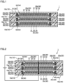
- Fig. 1 is a cross-sectional view showing a power storage module according to an embodiment of the present disclosure.
- a power storage module 1 according to the embodiment of the present disclosure includes a pair of electrode plates 10a and 10b, a sealing member 20a, a battery element 30a, and an insulating member 40a.
- Both of electrode plates 10a and 10b have electrical conductivity, and specifically, are made of metal.
- Each of electrode plates 10a and 10b has a positive electrode current collector plate and a negative electrode current collector plate.
- the positive electrode current collector plate and the negative electrode current collector plate are joined to each other by an adhesive layer.
- the positive electrode current collector plate of one electrode plate 10a of the pair of electrode plates 10a and 10b and the negative electrode current collector plate of the other electrode plate 10b face each other with battery element 30a interposed therebetween.
- electrode plate 10a may include only the positive electrode current collector plate and electrode plate 10b may include only the negative electrode current collector plate.
- the positive electrode current collector plate may include at least one selected from the group consisting of aluminum (Al), stainless steel, nickel (Ni), chromium (Cr), platinum (Pt), niobium (Nb), iron (Fe), titanium (Ti), and zinc (Zn).
- the positive electrode current collector plate is formed, for example, by a metal member such as Al foil.
- the negative electrode current collector plate may include at least one selected from the group consisting of aluminum (Al), stainless steel, nickel (Ni), chromium (Cr), platinum (Pt), niobium (Nb), iron (Fe), titanium (Ti), and zinc (Zn).
- the negative electrode current collector plate is formed, for example, by a metal member such as Al foil.
- Sealing member 20a is provided between the pair of electrode plates 10a and 10b to form a (first) space S1 together with the pair of electrode plates 10a and 10b.
- Space S1 is an enclosed space.
- Sealing member 20a has, for example, a rectangular cylindrical outer shape. Sealing member 20a is formed by curing a resin member such as a hot melt member, a thermoplastic resin, a thermosetting resin, or a photocurable resin. Examples of a material constituting sealing member 20a include a polyolefin-based resin such as polyethylene (PE) or polypropylene (PP), or a polyester-based resin such as polyethylene terephthalate (PET).
- PE polyethylene
- PP polypropylene
- PET polyethylene terephthalate
- Battery element 30a includes a positive electrode active material layer 31, a negative electrode active material layer 32, a separator 33, and an electrolyte 34.
- Positive electrode active material layer 31 is provided on a surface of one electrode plate 10a in space S1. Specifically, positive electrode active material layer 31 is provided on the positive electrode current collector plate of electrode plate 10a.
- the positive electrode active material layer includes a positive electrode active material, a conductive material and a binder.
- the positive electrode active material may include, for example, at least one selected from the group consisting of lithium cobalt oxide, lithium nickel oxide, lithium manganese oxide, lithium nickel cobalt manganese oxide (such as, for example, LiNi 1/3 Co 1/3 Mn 1/3 O 2 ), lithium nickel cobalt aluminate, and lithium iron phosphate.
- the conductive material may include, for example, at least one selected from the group consisting of carbon black (such as acetylene black), vapor grown carbon fiber (VGCF), carbon nanotube (CNT), and graphene flake.
- carbon black such as acetylene black
- VGCF vapor grown carbon fiber
- CNT carbon nanotube
- graphene flake graphene flake
- the binder may include, for example, at least one selected from the group consisting of carboxymethylcellulose (CMC), styrene-butadiene rubber (SBR), polyvinylidene fluoride (PVdF), and polytetrafluoroethylene (PTFE).
- CMC carboxymethylcellulose
- SBR styrene-butadiene rubber
- PVdF polyvinylidene fluoride
- PTFE polytetrafluoroethylene
- Negative electrode active material layer 32 is provided on a surface of the other electrode plate 10b in space S1. Specifically, negative electrode active material layer 32 is provided on the negative electrode current collector plate of electrode plate 10b.
- Negative electrode active material layer 32 includes a negative electrode active material and a binder.
- the negative electrode active material may be, for example, a carbon-based negative electrode active material such as natural graphite, easily graphitizable carbon or non-graphitizable carbon, or may be an alloy-based negative electrode active material containing silicon (Si), tin (Sn) or the like.
- Si silicon
- Sn tin
- a material that can be used as the binder included in the positive electrode active material layer can be used as the binder.
- Separator 33 is positioned between positive electrode active material layer 31 and negative electrode active material layer 32. Separator 33 is formed to have, for example, a sheet shape. Although not particularly limited, a thickness of separator 33 may be, for example, approximately 20 ⁇ m. Separator 33 is joined to sealing member 20. Therefore, space S1 is further partitioned into two spaces by separator 33.
- separator 33 examples include a porous film made of a polyolefin-based resin such as polyethylene (PE) or polypropylene (PP), woven or non-woven cloth made of a polyamide-based resin such as nylon and aromatic polyamide (aramid), polypropylene, polyethylene terephthalate (PET), or methylcellulose, or the like. Separator 33 may be reinforced with a vinylidene fluoride resin compound.
- a polyolefin-based resin such as polyethylene (PE) or polypropylene (PP)
- woven or non-woven cloth made of a polyamide-based resin such as nylon and aromatic polyamide (aramid), polypropylene, polyethylene terephthalate (PET), or methylcellulose, or the like.
- Separator 33 may be reinforced with a vinylidene fluoride resin compound.
- Separator 33 may have, for example, a multilayer structure, and specifically, may have a three-layer structure. Separator 33 may include, for example, a PP layer, a PE layer and a PP layer. The PP layer, the PE layer and the PP layer may be stacked in this order.
- Electrolyte 34 is arranged in space S1.
- electrolyte 34 is an electrolyte solution injected into space S1.
- electrolyte 34 is a non-aqueous electrolyte solution or a water-based electrolyte solution, and is, for example, a mixed solvent of EC/EMC/DMC.
- electrolyte 34 may be a solid electrolyte.
- electrolyte 34 is provided between positive electrode active material layer 31 and negative electrode active material layer 32, and battery element 30a may not be provided with the separator.
- Insulating member 40a is positioned between the pair of electrode plates 10a and 10b, insulating member 40a being provided on a side opposite to space S1 when viewed from sealing member 20a. It is preferable that insulating member 40a should be arranged such that the pair of electrode plates 10a and 10b do not directly face each other on the side opposite to space S1 when viewed from sealing member 20a. It is also preferable that insulating member 40a is arranged only in a space between the pair of electrode plates 10a and 10b.
- Examples of a material constituting insulating member 40a include a polyolefin-based resin such as polyethylene (PE) or polypropylene (PP), oils and fats such as paraffin, or the like.
- a polyolefin-based resin such as polyethylene (PE) or polypropylene (PP)
- oils and fats such as paraffin, or the like.
- a melting point of insulating member 40a is lower than a melting point of sealing member 20a.
- the melting point of insulating member 40a is preferably lower than a melting point of separator 33.
- a difference between the melting point of sealing member 20a and the melting point of insulating member 40a is preferably equal to or higher than 20°C, more preferably equal to or higher than 30°C, and further preferably equal to or higher than 40°C.
- the melting point of insulating member 40a is preferably higher than 60°C.
- the melting point of separator 33 is preferably equal to or higher than the melting point of sealing member 20a.
- electrolyte 34 When electrolyte 34 is a solid electrolyte, the operating temperature of power storage module 1 may reach a high temperature of approximately 80°C. Therefore, a sealing member and an insulating member that have melting points of 80°C or higher or 90°C or higher may be used as sealing member 20a and insulating member 40a.
- examples of a combination of sealing member 20a, separator 33 and insulating member 40a include the following combinations.
- sealing member 20a is PE (melting point of about 120°C) and separator 33 is a porous film made of PE (melting point of about 120°C) or PP (melting point of about 160°C), or woven or non-woven cloth made of aromatic polyamide (aramid) (melting point of about 200°C to 300°C), paraffin (melting point of about 70°C to 100°C) can be used as a material constituting insulating member 40a.
- PE melting point of about 120°C
- separator 33 is a porous film made of PE (melting point of about 120°C) or PP (melting point of about 160°C), or woven or non-woven cloth made of aromatic polyamide (aramid) (melting point of about 200°C to 300°C), paraffin (melting point of about 70°C to 100°C) can be used as a material constituting insulating member 40a.
- sealing member 20a is PP (melting point of about 160°C) and separator 33 is a porous film made of PP (melting point of about 160°C), or woven or non-woven cloth made of aromatic polyamide (aramid) (melting point of about 200°C to 300°C), paraffin (melting point of about 70°C to 100°C) or PE (melting point of about 120°C) can be used as a material constituting insulating member 40a.
- PP melting point of about 160°C
- separator 33 is a porous film made of PP (melting point of about 160°C), or woven or non-woven cloth made of aromatic polyamide (aramid) (melting point of about 200°C to 300°C), paraffin (melting point of about 70°C to 100°C) or PE (melting point of about 120°C)
- aromatic polyamide aromatic polyamide
- paraffin melting point of about 70°C to 100°C
- PE melting point of about 120°C
- sealing member 20a is PET (melting point of about 260°C) and separator 33 is woven or non-woven cloth made of aromatic polyamide (aramid) (melting point of about 200°C to 300°C), paraffin (melting point of about 70°C to 100°C) or PE (melting point of about 120°C) or PP (melting point of about 160°C) can be used as a material constituting insulating member 40a.
- aromatic polyamide aromatic polyamide
- paraffin melting point of about 70°C to 100°C
- PE melting point of about 120°C
- PP melting point of about 160°C
- Power storage module 1 according to the present embodiment includes three or more electrode plates 10 aligned in one direction. Three or more electrode plates 10 aligned in one direction include the pair of electrode plates 10a and 10b described above. Specifically, as shown in Fig. 1 , power storage module 1 according to the present embodiment includes four electrode plates 10. However, power storage module 1 according to the present embodiment may include five or more electrode plates 10.
- Power storage module 1 further includes a third electrode plate 10c positioned on a side opposite to the other electrode plate 10b (second electrode plate 10b) when viewed from one electrode plate 10a (first electrode plate 10a) of the pair of electrode plates 10.
- Power storage module 1 further includes a fourth electrode plate 10d positioned on a side opposite to first electrode plate 10a when viewed from second electrode plate 10b.
- Each of sealing member 20, battery element 30 and insulating member 40 is provided between electrode plates 10 that are adjacent to each other, of three or more electrode plates 10 (in the present embodiment, four electrode plates 10c, 10a, 10b, and 10d). That is, in the present embodiment, power storage module 1 includes a plurality of sealing members 20, a plurality of battery elements 30, and a plurality of insulating members 40. Power storage module 1 according to the present embodiment is a so-called bipolar battery.
- the plurality of sealing members 20 include (first) sealing member 20a, and further include a second sealing member 20b and a third sealing member 20c.
- Second sealing member 20b is provided between first electrode plate 10a and third electrode plate 10c to form a second space S2 together with first electrode plate 10a and third electrode plate 10c.
- Second space S2 is an enclosed space.
- Third sealing member 20c is provided between second electrode plate 10b and fourth electrode plate 10d to form a third space S3 together with second electrode plate 10b and fourth electrode plate 10d.
- Third space S3 is an enclosed space.
- the plurality of battery elements 30 include (first) battery element 30a, and further include a second battery element 30b and a third battery element 30c.
- Positive electrode active material layer 31 of second battery element 30b is provided on a surface of third electrode plate 10c in second space S2.
- Negative electrode active material layer 32 of second battery element 30b is provided on a surface of first electrode plate 10a in second space S2.
- Separator 33 is also positioned between these positive electrode active material layer 31 and negative electrode active material layer 32.
- Electrolyte 34 is also arranged in space S2.
- Positive electrode active material layer 31 of third battery element 30c is provided on a surface of second electrode plate 10b in third space S3.
- Negative electrode active material layer 32 of third battery element 30c is provided on a surface of fourth electrode plate 10d in third space S3.
- Separator 33 is also positioned between these positive electrode active material layer 31 and negative electrode active material layer 32.
- Electrolyte 34 is also arranged in space S3.
- the plurality of insulating members 40 include (first) insulating member 40a, and further include a second insulating member 40b and a third insulating member 40c.
- Second insulating member 40b is positioned between first electrode plate 10a and third electrode plate 10c, second insulating member 40b being provided on a side opposite to second space S2 when viewed from second sealing member 20b.
- Third insulating member 40c is positioned between second electrode plate 10b and fourth electrode plate 10d, third insulating member 40c being provided on a side opposite to third space S3 when viewed from third sealing member 20c.
- the plurality of insulating members 40 may be connected to each other on the lateral side of electrode plates 10.
- the plurality of insulating members 40 may be integrally formed by being connected to each other.
- Power storage module 1 may further include restraint members.
- the restraint members may restrain the plurality of electrode plates 10 and the plurality of battery elements 30 from the further outer sides of electrode plates 10 (in the present embodiment, third electrode plate 10c and fourth electrode plate 10d) located on the outermost side in a direction in which the plurality of electrode plates 10 are aligned (stacking direction in power storage module 1).
- Fig. 2 is a schematic cross-sectional view showing a state in which the power storage module according to the embodiment of the present disclosure is being charged. As shown in Fig. 2 , a voltage is applied to power storage module 1 from an external DC power supply, such that a charging current flows through power storage module 1. In Fig. 2 and the subsequent figures, the charging current is indicated by a thick black arrow.
- the charging current flows through third electrode plate 10c, second battery element 30b, first electrode plate 10a, first battery element 30a, second electrode plate 10b, third battery element 30c, and fourth electrode plate 10d in this order.
- each battery element 30 During charging of power storage module 1, the temperature of each battery element 30 increases. When the voltage is applied and the charging current continues to flow although power storage module 1 has already been fully charged, each battery element 30 generates heat excessively. Particularly, in the present embodiment, first battery element 30a positioned between second battery element 30b and third battery element 30c generates heat most excessively. The heat generation occurs more noticeably when battery element 30a is restrained by the above-described restraint members and expansion of battery element 30a is suppressed.
- Fig. 3 is a schematic cross-sectional view showing a state in which the power storage module according to the embodiment of the present disclosure has been overcharged and the first insulating member has melted away.
- insulating member 40a see Fig. 2
- the pair of electrode plates 10a and 10b face each other outside space S1. Electric discharge occurs between the pair of facing electrode plates 10a and 10b.
- first electrode plate 10a and second electrode plate 10b Due to the electric discharge between first electrode plate 10a and second electrode plate 10b, overcharging of the other battery elements 30 (in the present embodiment, second battery element 30b and third battery element 30c) in power storage module 1 continues.
- the charging current flows through third electrode plate 10c, second battery element 30b, first electrode plate 10a, second electrode plate 10b, third battery element 30c, and fourth electrode plate 10d in this order.
- second insulating member 40b and third insulating member 40c When the external short circuit occurs in first battery element 30a, the heat generated locally by this external short circuit is transmitted to second insulating member 40b and third insulating member 40c through first electrode plate 10a and second electrode plate 10b, respectively. As a result, the temperatures of second insulating member 40b and third insulating member 40c further increase temporarily. When the temperatures of second insulating member 40b and third insulating member 40c reach the respective melting points, second insulating member 40b and third insulating member 40c melt, and second insulating member 40b and third insulating member 40c also eventually melt away from between electrode plates 10.
- Fig. 4 is a schematic cross-sectional view showing a state in which the power storage module according to the embodiment of the present disclosure has been overcharged and the plurality of insulating members have melted away.
- second insulating member 40b see Fig. 3
- first electrode plate 10a and third electrode plate 10c face each other outside second space S2.
- Electric discharge occurs between first electrode plate 10a and third electrode plate 10c that face each other.
- the above-described electric discharge causes an external short circuit to occur in second battery element 30b.
- an SOC of second battery element 30b decreases forcibly.
- third insulating member 40c melts away, second electrode plate 10b and fourth electrode plate 10d face each other outside third space S3. Electric discharge occurs between second electrode plate 10b and fourth electrode plate 10d that face each other.
- the above-described electric discharge causes an external short circuit to occur in third battery element 30c.
- an SOC of third battery element 30c decreases forcibly.
Landscapes
- Chemical & Material Sciences (AREA)
- Chemical Kinetics & Catalysis (AREA)
- Electrochemistry (AREA)
- General Chemical & Material Sciences (AREA)
- Engineering & Computer Science (AREA)
- Manufacturing & Machinery (AREA)
- Materials Engineering (AREA)
- Sealing Battery Cases Or Jackets (AREA)
- Secondary Cells (AREA)
- Cell Separators (AREA)
Abstract
Description
- This nonprovisional application is based on
Japanese Patent Application No. 2023-019928 filed on February 13, 2023 - The present disclosure relates to a power storage module.
-
Japanese Patent Laying-Open No. 2022-081868 - There is a need of a power storage module that allows early suppression of a further increase in temperature when excessive heat generation occurs in the power storage module.
- The present disclosure has been made in light of the above-described problem, and an object of the present disclosure is to provide a power storage module that allows early suppression of a further increase in temperature.
- A power storage module according to the present disclosure includes: a pair of electrode plates; a sealing member; a battery element; and an insulating member. The sealing member is provided between the pair of electrode plates to form a space together with the pair of electrode plates. The battery element includes a positive electrode active material layer, a negative electrode active material layer and an electrolyte. The positive electrode active material layer is provided on a surface of one of the pair of electrode plates in the space. The negative electrode active material layer is provided on a surface of the other of the pair of electrode plates in the space. The insulating member is positioned between the pair of electrode plates, the insulating member being provided on a side opposite to the space when viewed from the sealing member. A melting point of the insulating member is lower than a melting point of the sealing member.
- According to this configuration, when the temperature of the battery element increases excessively, the insulating member melts before the sealing member melts. This causes the pair of electrode plates to face each other outside the space, and electric discharge occurs between the facing electrode plates. This electric discharge causes the battery element to be externally short-circuited, and a state of charge (SOC) of the battery element decreases forcibly. Therefore, a further increase in temperature of the battery element having the excessively increased temperature can be suppressed. Thus, it is possible to provide a power storage module that allows early suppression of a further increase in temperature.
- In the power storage module according to the present disclosure, the battery element may further include a separator positioned between the positive electrode active material layer and the negative electrode active material layer. It is preferable that the melting point of the insulating member should be lower than a melting point of the separator.
- According to this configuration, since the insulating member melts before an internal short circuit caused by melting of the separator occurs, the electrode plates face each other earlier outside the space and an external short circuit caused by electric discharge occurs earlier. Thus, an increase in temperature of the battery element can be suppressed earlier.
- In the power storage module according to the present disclosure, it is preferable that the melting point of the insulating member should be higher than 60°C.
- According to this configuration, when the temperature of the power storage module is equal to or lower than 60°C, which is a temperature at which the power storage module can operate relatively normally, melting of the insulating member can be prevented.
- The power storage module according to the present disclosure may further include three or more electrode plates including the pair of electrode plates, the three or more electrode plates being aligned in one direction. It is preferable that each of the sealing member, the battery element and the insulating member should be provided between the electrode plates that are adjacent to each other, of the three or more electrode plates.
- According to this configuration, heat generated by an external short circuit of the battery element having generated heat excessively is conveyed to a sealing member between electrode plates corresponding to another battery element. This heat causes the sealing member between the electrode plates corresponding to the other battery element to melt, and an external short circuit also occurs in the other battery element due to electric discharge between the electrode plates. Thus, an SOC of the power storage module as a whole decreases forcibly, and a further increase in temperature of the power storage module can be further suppressed.
- The foregoing and other objects, features, aspects and advantages of the present disclosure will become more apparent from the following detailed description of the present disclosure when taken in conjunction with the accompanying drawings.
-
-
Fig. 1 is a cross-sectional view showing a power storage module according to an embodiment of the present disclosure. -
Fig. 2 is a schematic cross-sectional view showing a state in which the power storage module according to the embodiment of the present disclosure is being charged. -
Fig. 3 is a schematic cross-sectional view showing a state in which the power storage module according to the embodiment of the present disclosure has been overcharged and a first insulating member has melted away. -
Fig. 4 is a schematic cross-sectional view showing a state in which the power storage module according to the embodiment of the present disclosure has been overcharged and a plurality of insulating members have melted away. - Hereinafter, a power storage module according to an embodiment of the present disclosure will be described with reference to the drawings. In the following description of the embodiment, the same or corresponding portions in the drawings are denoted by the same reference characters and description thereof will not be repeated.
-
Fig. 1 is a cross-sectional view showing a power storage module according to an embodiment of the present disclosure. As shown inFig. 1 , apower storage module 1 according to the embodiment of the present disclosure includes a pair ofelectrode plates sealing member 20a, abattery element 30a, and aninsulating member 40a. - Both of
electrode plates electrode plates electrode plate 10a of the pair ofelectrode plates other electrode plate 10b face each other withbattery element 30a interposed therebetween. - When
power storage module 1 includes only the pair ofelectrode plates electrode plate 10a may include only the positive electrode current collector plate andelectrode plate 10b may include only the negative electrode current collector plate. - The positive electrode current collector plate may include at least one selected from the group consisting of aluminum (Al), stainless steel, nickel (Ni), chromium (Cr), platinum (Pt), niobium (Nb), iron (Fe), titanium (Ti), and zinc (Zn). The positive electrode current collector plate is formed, for example, by a metal member such as Al foil.
- The negative electrode current collector plate may include at least one selected from the group consisting of aluminum (Al), stainless steel, nickel (Ni), chromium (Cr), platinum (Pt), niobium (Nb), iron (Fe), titanium (Ti), and zinc (Zn). The negative electrode current collector plate is formed, for example, by a metal member such as Al foil.
-
Sealing member 20a is provided between the pair ofelectrode plates electrode plates -
Sealing member 20a has, for example, a rectangular cylindrical outer shape. Sealingmember 20a is formed by curing a resin member such as a hot melt member, a thermoplastic resin, a thermosetting resin, or a photocurable resin. Examples of a material constitutingsealing member 20a include a polyolefin-based resin such as polyethylene (PE) or polypropylene (PP), or a polyester-based resin such as polyethylene terephthalate (PET). -
Battery element 30a includes a positive electrodeactive material layer 31, a negative electrodeactive material layer 32, aseparator 33, and anelectrolyte 34. - Positive electrode
active material layer 31 is provided on a surface of oneelectrode plate 10a in space S1. Specifically, positive electrodeactive material layer 31 is provided on the positive electrode current collector plate ofelectrode plate 10a. - The positive electrode active material layer includes a positive electrode active material, a conductive material and a binder. The positive electrode active material may include, for example, at least one selected from the group consisting of lithium cobalt oxide, lithium nickel oxide, lithium manganese oxide, lithium nickel cobalt manganese oxide (such as, for example, LiNi1/3Co1/3Mn1/3O2), lithium nickel cobalt aluminate, and lithium iron phosphate.
- The conductive material may include, for example, at least one selected from the group consisting of carbon black (such as acetylene black), vapor grown carbon fiber (VGCF), carbon nanotube (CNT), and graphene flake.
- The binder may include, for example, at least one selected from the group consisting of carboxymethylcellulose (CMC), styrene-butadiene rubber (SBR), polyvinylidene fluoride (PVdF), and polytetrafluoroethylene (PTFE).
- Negative electrode
active material layer 32 is provided on a surface of theother electrode plate 10b in space S1. Specifically, negative electrodeactive material layer 32 is provided on the negative electrode current collector plate ofelectrode plate 10b. - Negative electrode
active material layer 32 includes a negative electrode active material and a binder. The negative electrode active material may be, for example, a carbon-based negative electrode active material such as natural graphite, easily graphitizable carbon or non-graphitizable carbon, or may be an alloy-based negative electrode active material containing silicon (Si), tin (Sn) or the like. A material that can be used as the binder included in the positive electrode active material layer can be used as the binder. -
Separator 33 is positioned between positive electrodeactive material layer 31 and negative electrodeactive material layer 32.Separator 33 is formed to have, for example, a sheet shape. Although not particularly limited, a thickness ofseparator 33 may be, for example, approximately 20 µm.Separator 33 is joined to sealingmember 20. Therefore, space S1 is further partitioned into two spaces byseparator 33. - Examples of
separator 33 include a porous film made of a polyolefin-based resin such as polyethylene (PE) or polypropylene (PP), woven or non-woven cloth made of a polyamide-based resin such as nylon and aromatic polyamide (aramid), polypropylene, polyethylene terephthalate (PET), or methylcellulose, or the like.Separator 33 may be reinforced with a vinylidene fluoride resin compound. -
Separator 33 may have, for example, a multilayer structure, and specifically, may have a three-layer structure.Separator 33 may include, for example, a PP layer, a PE layer and a PP layer. The PP layer, the PE layer and the PP layer may be stacked in this order. -
Electrolyte 34 is arranged in space S1. In the present embodiment,electrolyte 34 is an electrolyte solution injected into space S1. Specifically,electrolyte 34 is a non-aqueous electrolyte solution or a water-based electrolyte solution, and is, for example, a mixed solvent of EC/EMC/DMC. Alternatively,electrolyte 34 may be a solid electrolyte. Whenelectrolyte 34 is a solid electrolyte,electrolyte 34 is provided between positive electrodeactive material layer 31 and negative electrodeactive material layer 32, andbattery element 30a may not be provided with the separator. - Insulating
member 40a is positioned between the pair ofelectrode plates member 40a being provided on a side opposite to space S1 when viewed from sealingmember 20a. It is preferable that insulatingmember 40a should be arranged such that the pair ofelectrode plates member 20a. It is also preferable that insulatingmember 40a is arranged only in a space between the pair ofelectrode plates - Examples of a material constituting insulating
member 40a include a polyolefin-based resin such as polyethylene (PE) or polypropylene (PP), oils and fats such as paraffin, or the like. - A melting point of insulating
member 40a is lower than a melting point of sealingmember 20a. In addition, the melting point of insulatingmember 40a is preferably lower than a melting point ofseparator 33. A difference between the melting point of sealingmember 20a and the melting point of insulatingmember 40a is preferably equal to or higher than 20°C, more preferably equal to or higher than 30°C, and further preferably equal to or higher than 40°C. Furthermore, considering that an example of the temperature at whichpower storage module 1 can operate normally is approximately 50°C or lower to 60°C or lower, the melting point of insulatingmember 40a is preferably higher than 60°C. The melting point ofseparator 33 is preferably equal to or higher than the melting point of sealingmember 20a. Whenelectrolyte 34 is a solid electrolyte, the operating temperature ofpower storage module 1 may reach a high temperature of approximately 80°C. Therefore, a sealing member and an insulating member that have melting points of 80°C or higher or 90°C or higher may be used as sealingmember 20a and insulatingmember 40a. - Considering the melting points of the materials described above, examples of a combination of sealing
member 20a,separator 33 and insulatingmember 40a include the following combinations. - When sealing
member 20a is PE (melting point of about 120°C) andseparator 33 is a porous film made of PE (melting point of about 120°C) or PP (melting point of about 160°C), or woven or non-woven cloth made of aromatic polyamide (aramid) (melting point of about 200°C to 300°C), paraffin (melting point of about 70°C to 100°C) can be used as a material constituting insulatingmember 40a. When sealingmember 20a is PP (melting point of about 160°C) andseparator 33 is a porous film made of PP (melting point of about 160°C), or woven or non-woven cloth made of aromatic polyamide (aramid) (melting point of about 200°C to 300°C), paraffin (melting point of about 70°C to 100°C) or PE (melting point of about 120°C) can be used as a material constituting insulatingmember 40a. When sealingmember 20a is PET (melting point of about 260°C) andseparator 33 is woven or non-woven cloth made of aromatic polyamide (aramid) (melting point of about 200°C to 300°C), paraffin (melting point of about 70°C to 100°C) or PE (melting point of about 120°C) or PP (melting point of about 160°C) can be used as a material constituting insulatingmember 40a. -
Power storage module 1 according to the present embodiment includes three ormore electrode plates 10 aligned in one direction. Three ormore electrode plates 10 aligned in one direction include the pair ofelectrode plates Fig. 1 ,power storage module 1 according to the present embodiment includes fourelectrode plates 10. However,power storage module 1 according to the present embodiment may include five ormore electrode plates 10. -
Power storage module 1 according to the present embodiment further includes athird electrode plate 10c positioned on a side opposite to theother electrode plate 10b (second electrode plate 10b) when viewed from oneelectrode plate 10a (first electrode plate 10a) of the pair ofelectrode plates 10.Power storage module 1 further includes afourth electrode plate 10d positioned on a side opposite tofirst electrode plate 10a when viewed fromsecond electrode plate 10b. - Each of sealing
member 20,battery element 30 and insulatingmember 40 is provided betweenelectrode plates 10 that are adjacent to each other, of three or more electrode plates 10 (in the present embodiment, fourelectrode plates power storage module 1 includes a plurality of sealingmembers 20, a plurality ofbattery elements 30, and a plurality of insulatingmembers 40.Power storage module 1 according to the present embodiment is a so-called bipolar battery. - The plurality of sealing
members 20 include (first) sealingmember 20a, and further include asecond sealing member 20b and athird sealing member 20c. - Second sealing
member 20b is provided betweenfirst electrode plate 10a andthird electrode plate 10c to form a second space S2 together withfirst electrode plate 10a andthird electrode plate 10c. Second space S2 is an enclosed space. Third sealingmember 20c is provided betweensecond electrode plate 10b andfourth electrode plate 10d to form a third space S3 together withsecond electrode plate 10b andfourth electrode plate 10d. Third space S3 is an enclosed space. - The plurality of
battery elements 30 include (first)battery element 30a, and further include asecond battery element 30b and athird battery element 30c. - Positive electrode
active material layer 31 ofsecond battery element 30b is provided on a surface ofthird electrode plate 10c in second space S2. Negative electrodeactive material layer 32 ofsecond battery element 30b is provided on a surface offirst electrode plate 10a in second space S2.Separator 33 is also positioned between these positive electrodeactive material layer 31 and negative electrodeactive material layer 32.Electrolyte 34 is also arranged in space S2. - Positive electrode
active material layer 31 ofthird battery element 30c is provided on a surface ofsecond electrode plate 10b in third space S3. Negative electrodeactive material layer 32 ofthird battery element 30c is provided on a surface offourth electrode plate 10d in third space S3.Separator 33 is also positioned between these positive electrodeactive material layer 31 and negative electrodeactive material layer 32.Electrolyte 34 is also arranged in space S3. - The plurality of insulating
members 40 include (first) insulatingmember 40a, and further include a second insulatingmember 40b and a third insulatingmember 40c. - Second insulating
member 40b is positioned betweenfirst electrode plate 10a andthird electrode plate 10c, second insulatingmember 40b being provided on a side opposite to second space S2 when viewed from second sealingmember 20b. Third insulatingmember 40c is positioned betweensecond electrode plate 10b andfourth electrode plate 10d, third insulatingmember 40c being provided on a side opposite to third space S3 when viewed from third sealingmember 20c. - The plurality of insulating
members 40 may be connected to each other on the lateral side ofelectrode plates 10. The plurality of insulatingmembers 40 may be integrally formed by being connected to each other. -
Power storage module 1 may further include restraint members. The restraint members may restrain the plurality ofelectrode plates 10 and the plurality ofbattery elements 30 from the further outer sides of electrode plates 10 (in the present embodiment,third electrode plate 10c andfourth electrode plate 10d) located on the outermost side in a direction in which the plurality ofelectrode plates 10 are aligned (stacking direction in power storage module 1). - Next, a state in which the temperature of
power storage module 1 according to the present embodiment has increased excessively will be described. -
Fig. 2 is a schematic cross-sectional view showing a state in which the power storage module according to the embodiment of the present disclosure is being charged. As shown inFig. 2 , a voltage is applied topower storage module 1 from an external DC power supply, such that a charging current flows throughpower storage module 1. InFig. 2 and the subsequent figures, the charging current is indicated by a thick black arrow. - In
power storage module 1, the charging current flows throughthird electrode plate 10c,second battery element 30b,first electrode plate 10a,first battery element 30a,second electrode plate 10b,third battery element 30c, andfourth electrode plate 10d in this order. - During charging of
power storage module 1, the temperature of eachbattery element 30 increases. When the voltage is applied and the charging current continues to flow althoughpower storage module 1 has already been fully charged, eachbattery element 30 generates heat excessively. Particularly, in the present embodiment,first battery element 30a positioned betweensecond battery element 30b andthird battery element 30c generates heat most excessively. The heat generation occurs more noticeably whenbattery element 30a is restrained by the above-described restraint members and expansion ofbattery element 30a is suppressed. - When the temperature of
battery element 30a increases excessively, the heat generated inbattery element 30a is transmitted to insulatingmember 40a through sealingmember 20a and the like. This also causes an increase in temperature of insulatingmember 40a. When the temperature of insulatingmember 40a reaches the melting point, insulatingmember 40a melts, and insulatingmember 40a eventually melts away from between the pair ofelectrode plates -
Fig. 3 is a schematic cross-sectional view showing a state in which the power storage module according to the embodiment of the present disclosure has been overcharged and the first insulating member has melted away. As shown inFig. 3 , when insulatingmember 40a (seeFig. 2 ) melts away, the pair ofelectrode plates electrode plates - The above-described electric discharge causes an external short circuit to occur in
battery element 30a. InFig. 3 and the subsequent figure, the external short circuit is indicated by a hollow arrow. As a result of the external short circuit, an SOC ofbattery element 30a decreases forcibly. Therefore, a further increase in temperature ofbattery element 30a having the excessively increased temperature can be suppressed. Thus, it is possible to providepower storage module 1 that allows early suppression of a further increase in temperature. - Due to the electric discharge between
first electrode plate 10a andsecond electrode plate 10b, overcharging of the other battery elements 30 (in the present embodiment,second battery element 30b andthird battery element 30c) inpower storage module 1 continues. The charging current flows throughthird electrode plate 10c,second battery element 30b,first electrode plate 10a,second electrode plate 10b,third battery element 30c, andfourth electrode plate 10d in this order. - When the external short circuit occurs in
first battery element 30a, the heat generated locally by this external short circuit is transmitted to second insulatingmember 40b and third insulatingmember 40c throughfirst electrode plate 10a andsecond electrode plate 10b, respectively. As a result, the temperatures of second insulatingmember 40b and third insulatingmember 40c further increase temporarily. When the temperatures of second insulatingmember 40b and third insulatingmember 40c reach the respective melting points, second insulatingmember 40b and third insulatingmember 40c melt, and second insulatingmember 40b and third insulatingmember 40c also eventually melt away from betweenelectrode plates 10. -
Fig. 4 is a schematic cross-sectional view showing a state in which the power storage module according to the embodiment of the present disclosure has been overcharged and the plurality of insulating members have melted away. As shown inFig. 4 , when second insulatingmember 40b (seeFig. 3 ) melts away,first electrode plate 10a andthird electrode plate 10c face each other outside second space S2. Electric discharge occurs betweenfirst electrode plate 10a andthird electrode plate 10c that face each other. The above-described electric discharge causes an external short circuit to occur insecond battery element 30b. As a result of the external short circuit, an SOC ofsecond battery element 30b decreases forcibly. - In addition, when third insulating
member 40c (seeFig. 3 ) melts away,second electrode plate 10b andfourth electrode plate 10d face each other outside third space S3. Electric discharge occurs betweensecond electrode plate 10b andfourth electrode plate 10d that face each other. The above-described electric discharge causes an external short circuit to occur inthird battery element 30c. As a result of the external short circuit, an SOC ofthird battery element 30c decreases forcibly. - As described above, since the SOC of at least one of
second battery element 30b andthird battery element 30c decreases forcibly, a further increase in temperature of at least one ofsecond battery element 30b andthird battery element 30c can be suppressed. Thus, an SOC ofpower storage module 1 as a whole decreases forcibly, and a further increase in temperature ofpower storage module 1 can be further suppressed. - In the description of the embodiment above, the combinable features may be combined with each other.
- Although the embodiment of the present disclosure has been described, it should be understood that the embodiment disclosed herein is illustrative and non-restrictive in every respect. The scope of the present disclosure is defined by the terms of the claims and is intended to include any modifications within the scope and meaning equivalent to the terms of the claims.
Claims (4)
- A power storage module comprising:a pair of electrode plates (10a, 10b);a sealing member (20) provided between the pair of electrode plates (10a, 10b) to form a space (S1) together with the pair of electrode plates (10a, 10b);a battery element (30) including a positive electrode active material layer (31) provided on a surface of one (10a) of the pair of electrode plates in the space (S1), a negative electrode active material layer (32) provided on a surface of the other (10b) of the pair of electrode plates in the space (S1), and an electrolyte (34); andan insulating member (40) positioned between the pair of electrode plates (10a, 10b), the insulating member (40) being provided on a side opposite to the space (S1) when viewed from the sealing member (20), whereina melting point of the insulating member (40) is lower than a melting point of the sealing member (20).
- The power storage module according to claim 1, whereinthe battery element (30) further includes a separator (33) positioned between the positive electrode active material layer (31) and the negative electrode active material layer (32), andthe melting point of the insulating member (40) is lower than a melting point of the separator (33).
- The power storage module according to claim 1 or 2, wherein
the melting point of the insulating member (40) is higher than 60°C. - The power storage module according to any one of claims 1 to 3, further comprisingthree or more electrode plates (10) including the pair of electrode plates (10a, 10b), the three or more electrode plates (10) being aligned in one direction, whereineach of the sealing member (20), the battery element (30) and the insulating member (40) is provided between the electrode plates (10) that are adjacent to each other, of the three or more electrode plates (10).
Applications Claiming Priority (1)
| Application Number | Priority Date | Filing Date | Title |
|---|---|---|---|
| JP2023019928A JP7679847B2 (en) | 2023-02-13 | 2023-02-13 | Energy Storage Module |
Publications (2)
| Publication Number | Publication Date |
|---|---|
| EP4415092A1 true EP4415092A1 (en) | 2024-08-14 |
| EP4415092B1 EP4415092B1 (en) | 2025-08-27 |
Family
ID=89542276
Family Applications (1)
| Application Number | Title | Priority Date | Filing Date |
|---|---|---|---|
| EP24150911.6A Active EP4415092B1 (en) | 2023-02-13 | 2024-01-09 | Power storage module |
Country Status (5)
| Country | Link |
|---|---|
| US (1) | US20240275000A1 (en) |
| EP (1) | EP4415092B1 (en) |
| JP (1) | JP7679847B2 (en) |
| KR (1) | KR20240126414A (en) |
| CN (1) | CN118486911A (en) |
Citations (5)
| Publication number | Priority date | Publication date | Assignee | Title |
|---|---|---|---|---|
| JP2021170486A (en) * | 2020-04-16 | 2021-10-28 | 株式会社豊田自動織機 | Power storage cell |
| WO2022102286A1 (en) * | 2020-11-11 | 2022-05-19 | 株式会社豊田自動織機 | Power storage module |
| JP2022081868A (en) | 2020-11-20 | 2022-06-01 | 株式会社豊田自動織機 | Power storage module |
| WO2022154005A1 (en) * | 2021-01-13 | 2022-07-21 | 株式会社豊田自動織機 | Power storage cell and power storage device |
| US20230261348A1 (en) * | 2022-02-17 | 2023-08-17 | Honda Motor Co., Ltd. | All-solid-state battery |
Family Cites Families (6)
| Publication number | Priority date | Publication date | Assignee | Title |
|---|---|---|---|---|
| JP4055640B2 (en) | 2003-04-28 | 2008-03-05 | 日産自動車株式会社 | Bipolar battery, bipolar battery manufacturing method, battery pack and vehicle |
| JP5092387B2 (en) | 2006-03-09 | 2012-12-05 | 日産自動車株式会社 | battery |
| JP5380990B2 (en) | 2008-10-01 | 2014-01-08 | 日産自動車株式会社 | Bipolar battery, assembled battery and vehicle using the bipolar battery |
| FR3006116B1 (en) | 2013-05-21 | 2015-06-26 | Commissariat Energie Atomique | BIPOLAR LI-ON BATTERY WITH IMPROVED SEALING AND METHOD OF MAKING THE SAME. |
| JP6579694B2 (en) | 2015-06-30 | 2019-09-25 | 日産自動車株式会社 | Secondary battery |
| JP7199033B2 (en) * | 2017-09-25 | 2023-01-05 | パナソニックIpマネジメント株式会社 | battery |
-
2023
- 2023-02-13 JP JP2023019928A patent/JP7679847B2/en active Active
-
2024
- 2024-01-04 US US18/403,917 patent/US20240275000A1/en active Pending
- 2024-01-09 EP EP24150911.6A patent/EP4415092B1/en active Active
- 2024-02-06 KR KR1020240018047A patent/KR20240126414A/en active Pending
- 2024-02-08 CN CN202410175675.3A patent/CN118486911A/en active Pending
Patent Citations (5)
| Publication number | Priority date | Publication date | Assignee | Title |
|---|---|---|---|---|
| JP2021170486A (en) * | 2020-04-16 | 2021-10-28 | 株式会社豊田自動織機 | Power storage cell |
| WO2022102286A1 (en) * | 2020-11-11 | 2022-05-19 | 株式会社豊田自動織機 | Power storage module |
| JP2022081868A (en) | 2020-11-20 | 2022-06-01 | 株式会社豊田自動織機 | Power storage module |
| WO2022154005A1 (en) * | 2021-01-13 | 2022-07-21 | 株式会社豊田自動織機 | Power storage cell and power storage device |
| US20230261348A1 (en) * | 2022-02-17 | 2023-08-17 | Honda Motor Co., Ltd. | All-solid-state battery |
Also Published As
| Publication number | Publication date |
|---|---|
| EP4415092B1 (en) | 2025-08-27 |
| JP7679847B2 (en) | 2025-05-20 |
| JP2024114267A (en) | 2024-08-23 |
| CN118486911A (en) | 2024-08-13 |
| US20240275000A1 (en) | 2024-08-15 |
| KR20240126414A (en) | 2024-08-20 |
Similar Documents
| Publication | Publication Date | Title |
|---|---|---|
| EP3352246B1 (en) | Solid electrolyte battery | |
| US10177387B2 (en) | Bipolar battery current collector that contracts to interrupt a flow of electric current in a direction thereof and bipolar battery | |
| US11824159B2 (en) | Anode-free solid-state battery and method of battery fabrication | |
| KR101451044B1 (en) | Bipolar battery | |
| EP3316349B1 (en) | Method for manufacturing electrochemical device | |
| JP7190314B2 (en) | bipolar secondary battery | |
| EP3595075B1 (en) | Secondary battery | |
| JP2004047239A (en) | Thin battery, assembled battery, composite assembled battery and vehicle equipped with the same | |
| JP3573141B2 (en) | Thin batteries, assembled batteries, composite assembled batteries and vehicles | |
| KR102804459B1 (en) | Electrode assembly and secondary battery including the same | |
| JP3711962B2 (en) | Thin battery | |
| JP5205713B2 (en) | Bipolar secondary battery | |
| JP2004055346A (en) | Battery pack, composite battery pack, and vehicle equipped with the same | |
| US11735776B2 (en) | Electrolytes for electrochemical cells | |
| JP4852882B2 (en) | Secondary battery and method for manufacturing secondary battery | |
| JP2013037863A (en) | Battery pack | |
| EP4415092B1 (en) | Power storage module | |
| CN113632280B (en) | Secondary battery and method for manufacturing the same | |
| JP3719235B2 (en) | Thin battery, assembled battery, composite assembled battery and vehicle | |
| JP2015225783A (en) | battery | |
| JP3852110B2 (en) | Thin battery and manufacturing method thereof | |
| JP5664068B2 (en) | Multilayer battery and method of manufacturing multilayer battery | |
| JP4052127B2 (en) | Thin battery support structure, assembled battery and vehicle | |
| KR20220131781A (en) | Electrode assembly and secondary battery including the same | |
| US20220407120A1 (en) | Battery |
Legal Events
| Date | Code | Title | Description |
|---|---|---|---|
| PUAI | Public reference made under article 153(3) epc to a published international application that has entered the european phase |
Free format text: ORIGINAL CODE: 0009012 |
|
| STAA | Information on the status of an ep patent application or granted ep patent |
Free format text: STATUS: REQUEST FOR EXAMINATION WAS MADE |
|
| 17P | Request for examination filed |
Effective date: 20240125 |
|
| AK | Designated contracting states |
Kind code of ref document: A1 Designated state(s): AL AT BE BG CH CY CZ DE DK EE ES FI FR GB GR HR HU IE IS IT LI LT LU LV MC ME MK MT NL NO PL PT RO RS SE SI SK SM TR |
|
| RIC1 | Information provided on ipc code assigned before grant |
Ipc: H01M 4/66 20060101ALN20250206BHEP Ipc: H01M 4/131 20100101ALN20250206BHEP Ipc: H01M 4/133 20100101ALN20250206BHEP Ipc: H01M 4/02 20060101ALN20250206BHEP Ipc: H01M 50/198 20210101ALI20250206BHEP Ipc: H01M 10/42 20060101ALI20250206BHEP Ipc: H01M 10/0585 20100101ALI20250206BHEP Ipc: H01M 50/474 20210101ALI20250206BHEP Ipc: H01M 50/186 20210101ALI20250206BHEP Ipc: H01M 10/04 20060101AFI20250206BHEP |
|
| GRAP | Despatch of communication of intention to grant a patent |
Free format text: ORIGINAL CODE: EPIDOSNIGR1 |
|
| STAA | Information on the status of an ep patent application or granted ep patent |
Free format text: STATUS: GRANT OF PATENT IS INTENDED |
|
| RIC1 | Information provided on ipc code assigned before grant |
Ipc: H01M 4/66 20060101ALN20250221BHEP Ipc: H01M 4/131 20100101ALN20250221BHEP Ipc: H01M 4/133 20100101ALN20250221BHEP Ipc: H01M 4/02 20060101ALN20250221BHEP Ipc: H01M 50/198 20210101ALI20250221BHEP Ipc: H01M 10/42 20060101ALI20250221BHEP Ipc: H01M 10/0585 20100101ALI20250221BHEP Ipc: H01M 50/474 20210101ALI20250221BHEP Ipc: H01M 50/186 20210101ALI20250221BHEP Ipc: H01M 10/04 20060101AFI20250221BHEP |
|
| INTG | Intention to grant announced |
Effective date: 20250318 |
|
| GRAS | Grant fee paid |
Free format text: ORIGINAL CODE: EPIDOSNIGR3 |
|
| GRAA | (expected) grant |
Free format text: ORIGINAL CODE: 0009210 |
|
| STAA | Information on the status of an ep patent application or granted ep patent |
Free format text: STATUS: THE PATENT HAS BEEN GRANTED |
|
| AK | Designated contracting states |
Kind code of ref document: B1 Designated state(s): AL AT BE BG CH CY CZ DE DK EE ES FI FR GB GR HR HU IE IS IT LI LT LU LV MC ME MK MT NL NO PL PT RO RS SE SI SK SM TR |
|
| REG | Reference to a national code |
Ref country code: CH Ref legal event code: EP |
|
| REG | Reference to a national code |
Ref country code: DE Ref legal event code: R096 Ref document number: 602024000513 Country of ref document: DE |
|
| REG | Reference to a national code |
Ref country code: IE Ref legal event code: FG4D |
|
| REG | Reference to a national code |
Ref country code: NL Ref legal event code: MP Effective date: 20250827 |
|
| PG25 | Lapsed in a contracting state [announced via postgrant information from national office to epo] |
Ref country code: IS Free format text: LAPSE BECAUSE OF FAILURE TO SUBMIT A TRANSLATION OF THE DESCRIPTION OR TO PAY THE FEE WITHIN THE PRESCRIBED TIME-LIMIT Effective date: 20251227 |
|
| PG25 | Lapsed in a contracting state [announced via postgrant information from national office to epo] |
Ref country code: NO Free format text: LAPSE BECAUSE OF FAILURE TO SUBMIT A TRANSLATION OF THE DESCRIPTION OR TO PAY THE FEE WITHIN THE PRESCRIBED TIME-LIMIT Effective date: 20251127 |
|
| REG | Reference to a national code |
Ref country code: LT Ref legal event code: MG9D |
|
| PG25 | Lapsed in a contracting state [announced via postgrant information from national office to epo] |
Ref country code: PT Free format text: LAPSE BECAUSE OF FAILURE TO SUBMIT A TRANSLATION OF THE DESCRIPTION OR TO PAY THE FEE WITHIN THE PRESCRIBED TIME-LIMIT Effective date: 20251229 |
|
| PG25 | Lapsed in a contracting state [announced via postgrant information from national office to epo] |
Ref country code: FI Free format text: LAPSE BECAUSE OF FAILURE TO SUBMIT A TRANSLATION OF THE DESCRIPTION OR TO PAY THE FEE WITHIN THE PRESCRIBED TIME-LIMIT Effective date: 20250827 |
|
| PG25 | Lapsed in a contracting state [announced via postgrant information from national office to epo] |
Ref country code: HR Free format text: LAPSE BECAUSE OF FAILURE TO SUBMIT A TRANSLATION OF THE DESCRIPTION OR TO PAY THE FEE WITHIN THE PRESCRIBED TIME-LIMIT Effective date: 20250827 Ref country code: NL Free format text: LAPSE BECAUSE OF FAILURE TO SUBMIT A TRANSLATION OF THE DESCRIPTION OR TO PAY THE FEE WITHIN THE PRESCRIBED TIME-LIMIT Effective date: 20250827 |
|
| PGFP | Annual fee paid to national office [announced via postgrant information from national office to epo] |
Ref country code: FR Payment date: 20251128 Year of fee payment: 3 |
|
| PG25 | Lapsed in a contracting state [announced via postgrant information from national office to epo] |
Ref country code: GR Free format text: LAPSE BECAUSE OF FAILURE TO SUBMIT A TRANSLATION OF THE DESCRIPTION OR TO PAY THE FEE WITHIN THE PRESCRIBED TIME-LIMIT Effective date: 20251128 |
|
| PG25 | Lapsed in a contracting state [announced via postgrant information from national office to epo] |
Ref country code: SE Free format text: LAPSE BECAUSE OF FAILURE TO SUBMIT A TRANSLATION OF THE DESCRIPTION OR TO PAY THE FEE WITHIN THE PRESCRIBED TIME-LIMIT Effective date: 20250827 |
|
| PG25 | Lapsed in a contracting state [announced via postgrant information from national office to epo] |
Ref country code: LV Free format text: LAPSE BECAUSE OF FAILURE TO SUBMIT A TRANSLATION OF THE DESCRIPTION OR TO PAY THE FEE WITHIN THE PRESCRIBED TIME-LIMIT Effective date: 20250827 |
|
| PG25 | Lapsed in a contracting state [announced via postgrant information from national office to epo] |
Ref country code: BG Free format text: LAPSE BECAUSE OF FAILURE TO SUBMIT A TRANSLATION OF THE DESCRIPTION OR TO PAY THE FEE WITHIN THE PRESCRIBED TIME-LIMIT Effective date: 20250827 Ref country code: PL Free format text: LAPSE BECAUSE OF FAILURE TO SUBMIT A TRANSLATION OF THE DESCRIPTION OR TO PAY THE FEE WITHIN THE PRESCRIBED TIME-LIMIT Effective date: 20250827 |
|
| PG25 | Lapsed in a contracting state [announced via postgrant information from national office to epo] |
Ref country code: RS Free format text: LAPSE BECAUSE OF FAILURE TO SUBMIT A TRANSLATION OF THE DESCRIPTION OR TO PAY THE FEE WITHIN THE PRESCRIBED TIME-LIMIT Effective date: 20251127 |
|
| PG25 | Lapsed in a contracting state [announced via postgrant information from national office to epo] |
Ref country code: ES Free format text: LAPSE BECAUSE OF FAILURE TO SUBMIT A TRANSLATION OF THE DESCRIPTION OR TO PAY THE FEE WITHIN THE PRESCRIBED TIME-LIMIT Effective date: 20250827 |
|
| REG | Reference to a national code |
Ref country code: AT Ref legal event code: MK05 Ref document number: 1831069 Country of ref document: AT Kind code of ref document: T Effective date: 20250827 |
|
| PG25 | Lapsed in a contracting state [announced via postgrant information from national office to epo] |
Ref country code: SM Free format text: LAPSE BECAUSE OF FAILURE TO SUBMIT A TRANSLATION OF THE DESCRIPTION OR TO PAY THE FEE WITHIN THE PRESCRIBED TIME-LIMIT Effective date: 20250827 |
|
| PG25 | Lapsed in a contracting state [announced via postgrant information from national office to epo] |
Ref country code: DK Free format text: LAPSE BECAUSE OF FAILURE TO SUBMIT A TRANSLATION OF THE DESCRIPTION OR TO PAY THE FEE WITHIN THE PRESCRIBED TIME-LIMIT Effective date: 20250827 |
|
| PGFP | Annual fee paid to national office [announced via postgrant information from national office to epo] |
Ref country code: DE Payment date: 20251203 Year of fee payment: 3 |
|
| PG25 | Lapsed in a contracting state [announced via postgrant information from national office to epo] |
Ref country code: AT Free format text: LAPSE BECAUSE OF FAILURE TO SUBMIT A TRANSLATION OF THE DESCRIPTION OR TO PAY THE FEE WITHIN THE PRESCRIBED TIME-LIMIT Effective date: 20250827 |
|
| PG25 | Lapsed in a contracting state [announced via postgrant information from national office to epo] |
Ref country code: IT Free format text: LAPSE BECAUSE OF FAILURE TO SUBMIT A TRANSLATION OF THE DESCRIPTION OR TO PAY THE FEE WITHIN THE PRESCRIBED TIME-LIMIT Effective date: 20250827 |
|
| PG25 | Lapsed in a contracting state [announced via postgrant information from national office to epo] |
Ref country code: CZ Free format text: LAPSE BECAUSE OF FAILURE TO SUBMIT A TRANSLATION OF THE DESCRIPTION OR TO PAY THE FEE WITHIN THE PRESCRIBED TIME-LIMIT Effective date: 20250827 |
|
| PG25 | Lapsed in a contracting state [announced via postgrant information from national office to epo] |
Ref country code: SK Free format text: LAPSE BECAUSE OF FAILURE TO SUBMIT A TRANSLATION OF THE DESCRIPTION OR TO PAY THE FEE WITHIN THE PRESCRIBED TIME-LIMIT Effective date: 20250827 Ref country code: EE Free format text: LAPSE BECAUSE OF FAILURE TO SUBMIT A TRANSLATION OF THE DESCRIPTION OR TO PAY THE FEE WITHIN THE PRESCRIBED TIME-LIMIT Effective date: 20250827 |