EP4414822B1 - Mehrdimensionaler festkörperantriebsblockzugriff - Google Patents
Mehrdimensionaler festkörperantriebsblockzugriff Download PDFInfo
- Publication number
- EP4414822B1 EP4414822B1 EP24155617.4A EP24155617A EP4414822B1 EP 4414822 B1 EP4414822 B1 EP 4414822B1 EP 24155617 A EP24155617 A EP 24155617A EP 4414822 B1 EP4414822 B1 EP 4414822B1
- Authority
- EP
- European Patent Office
- Prior art keywords
- dimension
- namespace
- contiguous block
- blocks
- block region
- Prior art date
- Legal status (The legal status is an assumption and is not a legal conclusion. Google has not performed a legal analysis and makes no representation as to the accuracy of the status listed.)
- Active
Links
Images

Classifications
-
- G—PHYSICS
- G06—COMPUTING OR CALCULATING; COUNTING
- G06F—ELECTRIC DIGITAL DATA PROCESSING
- G06F12/00—Accessing, addressing or allocating within memory systems or architectures
- G06F12/02—Addressing or allocation; Relocation
- G06F12/0207—Addressing or allocation; Relocation with multidimensional access, e.g. row/column, matrix
-
- G—PHYSICS
- G06—COMPUTING OR CALCULATING; COUNTING
- G06F—ELECTRIC DIGITAL DATA PROCESSING
- G06F12/00—Accessing, addressing or allocating within memory systems or architectures
- G06F12/02—Addressing or allocation; Relocation
- G06F12/0223—User address space allocation, e.g. contiguous or non contiguous base addressing
- G06F12/023—Free address space management
- G06F12/0238—Memory management in non-volatile memory, e.g. resistive RAM or ferroelectric memory
- G06F12/0246—Memory management in non-volatile memory, e.g. resistive RAM or ferroelectric memory in block erasable memory, e.g. flash memory
-
- G—PHYSICS
- G06—COMPUTING OR CALCULATING; COUNTING
- G06F—ELECTRIC DIGITAL DATA PROCESSING
- G06F3/00—Input arrangements for transferring data to be processed into a form capable of being handled by the computer; Output arrangements for transferring data from processing unit to output unit, e.g. interface arrangements
- G06F3/06—Digital input from, or digital output to, record carriers, e.g. RAID, emulated record carriers or networked record carriers
- G06F3/0601—Interfaces specially adapted for storage systems
- G06F3/0602—Interfaces specially adapted for storage systems specifically adapted to achieve a particular effect
- G06F3/0604—Improving or facilitating administration, e.g. storage management
-
- G—PHYSICS
- G06—COMPUTING OR CALCULATING; COUNTING
- G06F—ELECTRIC DIGITAL DATA PROCESSING
- G06F3/00—Input arrangements for transferring data to be processed into a form capable of being handled by the computer; Output arrangements for transferring data from processing unit to output unit, e.g. interface arrangements
- G06F3/06—Digital input from, or digital output to, record carriers, e.g. RAID, emulated record carriers or networked record carriers
- G06F3/0601—Interfaces specially adapted for storage systems
- G06F3/0602—Interfaces specially adapted for storage systems specifically adapted to achieve a particular effect
- G06F3/061—Improving I/O performance
-
- G—PHYSICS
- G06—COMPUTING OR CALCULATING; COUNTING
- G06F—ELECTRIC DIGITAL DATA PROCESSING
- G06F3/00—Input arrangements for transferring data to be processed into a form capable of being handled by the computer; Output arrangements for transferring data from processing unit to output unit, e.g. interface arrangements
- G06F3/06—Digital input from, or digital output to, record carriers, e.g. RAID, emulated record carriers or networked record carriers
- G06F3/0601—Interfaces specially adapted for storage systems
- G06F3/0628—Interfaces specially adapted for storage systems making use of a particular technique
- G06F3/0638—Organizing or formatting or addressing of data
- G06F3/064—Management of blocks
-
- G—PHYSICS
- G06—COMPUTING OR CALCULATING; COUNTING
- G06F—ELECTRIC DIGITAL DATA PROCESSING
- G06F3/00—Input arrangements for transferring data to be processed into a form capable of being handled by the computer; Output arrangements for transferring data from processing unit to output unit, e.g. interface arrangements
- G06F3/06—Digital input from, or digital output to, record carriers, e.g. RAID, emulated record carriers or networked record carriers
- G06F3/0601—Interfaces specially adapted for storage systems
- G06F3/0628—Interfaces specially adapted for storage systems making use of a particular technique
- G06F3/0638—Organizing or formatting or addressing of data
- G06F3/0644—Management of space entities, e.g. partitions, extents, pools
-
- G—PHYSICS
- G06—COMPUTING OR CALCULATING; COUNTING
- G06F—ELECTRIC DIGITAL DATA PROCESSING
- G06F3/00—Input arrangements for transferring data to be processed into a form capable of being handled by the computer; Output arrangements for transferring data from processing unit to output unit, e.g. interface arrangements
- G06F3/06—Digital input from, or digital output to, record carriers, e.g. RAID, emulated record carriers or networked record carriers
- G06F3/0601—Interfaces specially adapted for storage systems
- G06F3/0628—Interfaces specially adapted for storage systems making use of a particular technique
- G06F3/0655—Vertical data movement, i.e. input-output transfer; data movement between one or more hosts and one or more storage devices
-
- G—PHYSICS
- G06—COMPUTING OR CALCULATING; COUNTING
- G06F—ELECTRIC DIGITAL DATA PROCESSING
- G06F3/00—Input arrangements for transferring data to be processed into a form capable of being handled by the computer; Output arrangements for transferring data from processing unit to output unit, e.g. interface arrangements
- G06F3/06—Digital input from, or digital output to, record carriers, e.g. RAID, emulated record carriers or networked record carriers
- G06F3/0601—Interfaces specially adapted for storage systems
- G06F3/0628—Interfaces specially adapted for storage systems making use of a particular technique
- G06F3/0655—Vertical data movement, i.e. input-output transfer; data movement between one or more hosts and one or more storage devices
- G06F3/0659—Command handling arrangements, e.g. command buffers, queues, command scheduling
-
- G—PHYSICS
- G06—COMPUTING OR CALCULATING; COUNTING
- G06F—ELECTRIC DIGITAL DATA PROCESSING
- G06F3/00—Input arrangements for transferring data to be processed into a form capable of being handled by the computer; Output arrangements for transferring data from processing unit to output unit, e.g. interface arrangements
- G06F3/06—Digital input from, or digital output to, record carriers, e.g. RAID, emulated record carriers or networked record carriers
- G06F3/0601—Interfaces specially adapted for storage systems
- G06F3/0668—Interfaces specially adapted for storage systems adopting a particular infrastructure
- G06F3/0671—In-line storage system
- G06F3/0673—Single storage device
- G06F3/0679—Non-volatile semiconductor memory device, e.g. flash memory, one time programmable memory [OTP]
-
- G—PHYSICS
- G06—COMPUTING OR CALCULATING; COUNTING
- G06F—ELECTRIC DIGITAL DATA PROCESSING
- G06F3/00—Input arrangements for transferring data to be processed into a form capable of being handled by the computer; Output arrangements for transferring data from processing unit to output unit, e.g. interface arrangements
- G06F3/06—Digital input from, or digital output to, record carriers, e.g. RAID, emulated record carriers or networked record carriers
- G06F3/0601—Interfaces specially adapted for storage systems
- G06F3/0668—Interfaces specially adapted for storage systems adopting a particular infrastructure
- G06F3/0671—In-line storage system
- G06F3/0683—Plurality of storage devices
-
- G—PHYSICS
- G06—COMPUTING OR CALCULATING; COUNTING
- G06F—ELECTRIC DIGITAL DATA PROCESSING
- G06F2212/00—Indexing scheme relating to accessing, addressing or allocation within memory systems or architectures
- G06F2212/10—Providing a specific technical effect
- G06F2212/1016—Performance improvement
-
- G—PHYSICS
- G06—COMPUTING OR CALCULATING; COUNTING
- G06F—ELECTRIC DIGITAL DATA PROCESSING
- G06F2212/00—Indexing scheme relating to accessing, addressing or allocation within memory systems or architectures
- G06F2212/72—Details relating to flash memory management
- G06F2212/7201—Logical to physical mapping or translation of blocks or pages
-
- G—PHYSICS
- G06—COMPUTING OR CALCULATING; COUNTING
- G06F—ELECTRIC DIGITAL DATA PROCESSING
- G06F2212/00—Indexing scheme relating to accessing, addressing or allocation within memory systems or architectures
- G06F2212/72—Details relating to flash memory management
- G06F2212/7204—Capacity control, e.g. partitioning, end-of-life degradation
-
- G—PHYSICS
- G06—COMPUTING OR CALCULATING; COUNTING
- G06F—ELECTRIC DIGITAL DATA PROCESSING
- G06F2212/00—Indexing scheme relating to accessing, addressing or allocation within memory systems or architectures
- G06F2212/72—Details relating to flash memory management
- G06F2212/7208—Multiple device management, e.g. distributing data over multiple flash devices
Definitions
- aspects of the present disclosure are directed to improving access efficiency for solid state drives.
- a method for accessing blocks of a solid state drive comprises receiving a starting position that identifies a first block of a contiguous block region within a namespace of the solid state drive to be accessed according to a single input/output operation, where the namespace comprises two dimensions of logical address space with respective indices for indexing blocks within a corresponding dimension of the logical address space.
- the method further comprises receiving a first dimensional identifier that identifies a size of the contiguous block region in a first dimension of the namespace, and a second dimensional identifier that identifies a size of the contiguous block region in a second dimension of the namespace.
- the method further comprises accessing blocks of the contiguous block region in response to the single input/output operation according to the starting position, the first dimensional identifier, and the second dimensional identifier.
- a system for accessing blocks of a solid state drive comprises one or more NAND memory chips for data storage.
- the system further comprises a drive storage controller configured to access the one or more NAND memory chips and configure the one or more NAND memory chips with a namespace that comprises two dimensions of logical address space with respective indices for indexing blocks within a corresponding dimension of the logical address space.
- a solid state drive is configured for block access using multiple dimensions, such as first and second dimensions. This allows for access to a contiguous block region within the solid state drive, even when that contiguous block region is not sequential in a single dimension.
- a starting position is received, where the starting position identifies a first block of the contiguous block region to be accessed according to a single input/output operation.
- a first dimensional identifier is received that identifies a size of the contiguous block region in a first dimension
- a second dimensional identifier is received that identifies a size of the contiguous block region in a second dimension.
- Blocks of the contiguous block region are accessed in response to the single input/output operation according to the starting position, the first dimensional identifier, and the second dimensional identifier.
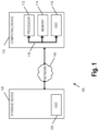
- FIG. 1 shows a block diagram of an example of a system configuration for a solid state drive, according to an example embodiment.
- the system 100 includes a computing device 110 that is configured to access blocks of a solid state drive.
- the system 100 may also include a storage device 120 that is communicatively coupled with the computing device 110 via a network 140, in some examples.
- the computing device 110 may be any type of computing device, including a smartphone, mobile computer or mobile computing device (e.g., a Microsoft ® Surface ® device, a laptop computer, a notebook computer, a tablet computer such as an Apple iPad TM , a netbook, etc.), or a stationary computing device such as a desktop computer or PC (personal computer).
- the computing device 110 may be configured to communicate with a the storage device 120, for example, using the network 140 (e.g., the Intemet, a local area network, etc.).
- the network 140 e.g., the Intemet, a local area network, etc.
- the computing device 110 may be configured to execute one or more software applications (or "applications”) and/or services and/or manage hardware resources (e.g., processors, memory, etc.), which may be utilized by users of the computing device 110 or processes running on the computing device 110.
- software applications or "applications”
- hardware resources e.g., processors, memory, etc.
- Computing device 110 comprises a processor 112, a memory 114, and a solid state drive (SSD) 116.
- the processor 112 may be any suitable microprocessor (e.g., x86-64 based processor, ARM based processor) along with suitable memory 114 (e.g., double data rate random access memory, embedded memory).
- the processor 112 is implemented as a system on a chip (SoC), with or without the memory 114.
- SoC system on a chip
- the processor 112 comprises or communicates with a secondary storage controller or host controller configured to communicate with storage devices, such as the SSD 116.
- the processor 112 supports one or more logical device interfaces, such as advanced host controller interface (AHCI), non-volatile memory express (NVMe) interface (or non-volatile memory host controller interface specification), or other suitable logical device interface.
- AHCI advanced host controller interface
- NVMe non-volatile memory express
- the SSD 116 (or semiconductor storage device) is a solid-state storage device that uses integrated circuit assemblies to store data.
- the SSD 116 may be used as a secondary storage device for the computing device 110 and may be implemented as a flash memory module, USB memory card, M.2 SSD or other suitable module having one or more NAND flash chips or NOR flash chips. Further details of the SSD 116 are described below with respect to Fig. 2 .
- the processor 112, memory 114, and the SSD 116 are generally communicatively coupled by an interconnect bus 118, such as a Peripheral Component Interconnect Express (PCIe) bus or M-PHY bus.
- the interconnect bus 118 is a serial bus, parallel bus, or other suitable communication bus for sending and receiving data with the SSD 116.
- Storage device 120 may include one or more solid state drives 126 or other suitable storage mechanisms (not shown).
- the solid state drive 126 may generally correspond to the SSD 116, in some examples.
- the storage device 120 may be a network attached storage device, cloud storage device, or other remotely accessible storage device containing one or more solid state drives, in various examples.
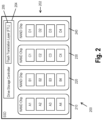
- Fig. 2 shows a block diagram of an example of a solid state drive (SSD) 200, according to an example embodiment.
- the SSD 200 corresponds to the SSD 116 and may be implemented as a hard drive, memory card, universal serial bus (USB) flash drive, embedded storage drive, or other suitable storage device.
- the SSD 200 comprises one or more memory chips 202 and a drive storage controller 204.
- the SSD 200 comprises four NAND flash chips 210, 220, 230, and 240.
- the SSD 200 comprises one, two, three, or more NAND flash chips.
- the SSD 200 uses NOR flash chips instead of, or in addition to, the NAND flash chips.
- the NAND flash chips 210, 220, 230, and 240 generally comprise cells for storing data. Each cell may store one, two, three, or more bits and the cells may be arranged in blocks.
- the drive storage controller 204 is configured to access and configure the NAND memory chips 210, 220, 230, and 240 with one or more namespaces, as described herein.
- the features of the drive storage controller 204 are implemented within a flash translation layer 206 of the drive storage controller 204.
- the flash translation layer (FTL) generally performs logical-to-physical address translation, along with other maintenance tasks such as garbage collection, wear-leveling, bad block management, etc.
- the drive storage controller 204 may be a non-volatile memory express (NVMe) controller, universal flash storage (UFS) controller, or other suitable controller for memory chips. Generally, the drive storage controller 204 supports commands that provide access to user data stored on the memory chips using an input/output (I/O) command set. In some examples, the drive storage controller 204 is implemented as one or more primary controllers and one or more secondary controllers that are each dependent upon a primary controller. The drive storage controller 204 may also comprise a cache for operational use. The cache may be implemented as a random access memory module within the drive storage controller 204, as allocated or reserved blocks in the memory chips 202, or a combination thereof, in various examples.
- NVMe non-volatile memory express
- UFS universal flash storage
- the drive storage controller 204 may also comprise a cache for operational use.
- the cache may be implemented as a random access memory module within the drive storage controller 204, as allocated or reserved blocks in the memory chips 202, or a combination thereof, in various examples.
- the drive storage controller 204 is configured to support a multi-dimensional logical address space, for example, a two-dimensional logical address space as described below with respect to Fig. 3 , a three-dimensional logical address space, a four-dimensional logical address space, etc.
- Each dimension has a corresponding index for indexing blocks within that dimension of the logical address space.
- a two-dimensional logical address space may be modeled as rows and columns where a first index identifies a location of a block in the first dimension (i.e., a row) and a second index identifies a location of a block in the second dimension (i.e., a column), for example.
- a three-dimensional logical address space may be modeled as rows, columns, and tubes, for example.
- the drive storage controller 204 generally creates a namespace as a formatted quantity of non-volatile memory that may be directly accessed by a host and comprises one or more logical blocks.
- a logical block is a smallest unit of data that may be read from or written by the drive storage controller 204.
- Logical block sizes may be 512 bytes, 1 KiB, 2 KiB, 4 KiB, 8 KiB, or another suitable size, in various examples.
- the individual blocks may be modeled as cells in a table or spreadsheet. In the example shown in Fig.
- the NAND flash chip 210 comprises four blocks in a single column, labeled as logical blocks A1, A2, A3, and A4, the NAND flash chip 220 comprises four blocks in a single column, labeled as B1, B2, B3, and B4, and so on.
- the SSD 200 comprises sixteen blocks which may be modeled as a 4 x 4 table. In contrast to a one-dimensional address space where sixteen blocks may be accessed using a single address (e.g., hexadecimal x00, x01, x02, ...
- the drive storage controller 204 is configured to use a two-dimensional logical address space and as such, a first dimensional identifier, such as letters A through D, may be used to indicate a column, and a second dimensional identifier, such as number 1 through 4, may be used to indicate a row.
- a first dimensional identifier such as letters A through D
- a second dimensional identifier such as number 1 through 4
- the memory chips 202 are shown with only a single column of blocks, the memory chips may have any suitable arrangement of blocks with one or more rows, one or more columns, etc., in other examples.
- the NAND chips may have three dimensions using multiple layers vertically (i.e., 3D NAND chips).
- the drive storage controller 204 supports multiple input/output (I/O) command sets, for example, an enhanced command set with two-dimensional commands and a legacy command set with one-dimensional commands.
- I/O input/output
- a first primary controller (not shown) is configured to use two-dimensional commands (i.e., rows and columns) to access the memory chips 202
- a second primary controller (not shown) is configured to use one-dimensional commands (i.e., hexadecimal) to access the memory chips 202.
- a single primary controller is configured to use both one-dimensional and two-dimensional command sets.
- Fig. 3 shows a diagram of an example namespace 300 of a solid state drive for two-dimensional access, according to an example embodiment.
- the namespace 300 may be mapped to all or some of the blocks within the SSD 200, for example, by the drive storage controller 204.
- the SSD 200 may be configured with one, two, three, or more namespaces in various examples or scenarios.
- the SSD 200 may be configured with only two-dimensional (or multi-dimensional) namespaces, or both one-dimensional and multi-dimensional namespaces, in various examples or scenarios.
- the drive storage controller 204 is implemented as an NVMe-compatible drive storage controller and configures the namespace 300.
- the drive storage controller 204 uses and/or supports commands that are similar or based upon commands in the NVM Express Base Specification (see nvmexpress.org).
- Example commands or data structures that may be modified to support multi-dimensional logical address spaces comprise the starting logical block address (SLBA), number of logical blocks (NLB), or namespace size (NSZE) field.
- Other commands may be used in different implementations of the drive storage controller 204 (e.g., in the case of AHCI).
- a namespace size (NSZE) field may indicate the total size of the namespace 300 as a total size in rows and columns (Max_Row, Max_Col) instead of in a number of logical blocks (LBA 0 through n-1, for example).
- the drive storage controller 204 receives a plurality of I/O operations from an application, operating system, driver, etc. that provides a one-dimensional address for several operations of a same type (e.g., read operations, write operations). In one example, the drive storage controller 204 converts multiple I/O operations of the same type into a single I/O operation using the two-dimensional logical block address commands. Using the example of Fig. 2 , read operations such as READ(B1), READ(B2), READ(B3) may be converted into a single read operation as READ(B1, (1, 3)) for a read operation starting at block B1 and continuing for 1 column and 3 rows. Other conversions of operations will be apparent to those skilled in the art.
- an SSD driver (e.g., SSD driver 621) of an operating system or application module converts multiple I/O operations of the same type into a single I/O operation using the two-dimensional logical block address commands.
- the SSD driver 621 may then provide the converted commands to the drive storage controller 204.
- the SSD driver provides an interface that comprises two-dimensional logical block address commands to other application modules.
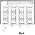
- Fig. 4 shows a diagram of an example logical to physical mapping for two-dimensional access of an SSD 400, according to an example embodiment.
- the SSD 400 generally correspond to the SSD 200, but with updated block identifiers showing a mapping of the logical blocks shown in Fig. 2 onto physical blocks of the memory chips 210, 220, 230, and 240.
- a horizontal READ((0,0), (1, 4)) operation using the logical address space in Fig. 2 would read a single row as A1, B1, C1, and D1. This operation corresponds to a horizontal read from physical blocks A1, B1, C1, and D1, from memory chips 210, 220, 230, and 240, respectively.
- a horizontal READ((1,0), (1, 4)) operation using the logical address space in Fig. 2 would read a single row as A2, B2, C2, and D2.
- This operation corresponds to a horizontal read from physical blocks D2, A2, B2, C2, from memory chips 210, 220, 230, and 240, respectively.
- the physical blocks are read out of sequential order, they may be read simultaneously because they are located on different chips.
- the mapping from the logical address space to physical address space of Fig. 4 corresponds to an offset of a column index by an amount of the row index.
- the offset of the column index is 0 for the first row, 1 for the second row (shifting the physical location one chip to the right), 2 for the second row (shifting the physical location two chips to the right), etc.
- Other variations in offset will be apparent to those skilled in the art, such as an offset of the row index by an amount of the column index, offsets in a different direction, etc.
- the offset is dynamically determined when configuring a namespace.
- the mapping shown in Fig. 4 indicates that a vertical READ((0,0), (4,1)) operation using the logical address space in Fig. 2 would read a single column as A1, A2, A3, and A4.
- This operation corresponds to a vertical read from physical blocks A1, A2, A3, and A4 from memory chips 210, 220, 230, and 240, respectively.
- the physical blocks may be read simultaneously because they are located on different chips, instead of each block being located on the first memory chip 210.
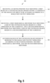
- Fig. 5 shows a flowchart of an example method of accessing blocks of a solid state drive, according to an example embodiment.
- Technical processes shown in these figures will be performed automatically unless otherwise indicated. In any given embodiment, some steps of a process may be repeated, perhaps with different parameters or data to operate on. Steps in an embodiment may also be performed in a different order than the top-to-bottom order that is laid out in Fig. 5 . Steps may be performed serially, in a partially overlapping manner, or fully in parallel. Thus, the order in which steps of method 500 are performed may vary from one performance to the process of another performance of the process.
- Steps may also be omitted, combined, renamed, regrouped, be performed on one or more machines, or otherwise depart from the illustrated flow, provided that the process performed is operable and conforms to at least one claim.
- the steps of Fig. 5 may be performed by the computing device 110 (e.g., via the drive storage controller 204), an SSD controller 618 ( Fig. 6 ), or other suitable computing device.
- Method 500 begins with step 502.
- a starting position is received that identifies a first block of a contiguous block region within a namespace of the solid state drive to be accessed according to a single input/output operation.
- the namespace comprises two dimensions.
- the starting position may be a tuple such as (5, 3) for the block 312 for the namespace 300 shown in Fig. 3 , received by the drive storage controller 204.
- a first dimensional identifier that identifies a size of the contiguous block region in a first dimension of the namespace is received
- a second dimensional identifier that identifies a size of the contiguous block region in a second dimension of the namespace is received.
- the drive storage controller 204 may receive a tuple for a number of logical rows (NLR) and a number of logical columns (NLC).
- blocks of the contiguous block region are accessed in response to the single input/output operation according to the starting position, the first dimensional identifier, and the second dimensional identifier.
- the drive storage controller 204 may perform a read operation, write operation, format operation, or other suitable operation on the contiguous block region 310.
- the method 500 further comprises receiving an access order that prioritizes one of the first dimension or the second dimension, and accessing each of the blocks of the block region in the prioritized dimension from the first block before accessing remaining blocks of the contiguous block region.
- the drive storage controller 204 may receive an access order indicating a row-first or column-first manner of accessing the blocks of the contiguous block region 310.
- the starting position comprises a 2-tuple having a first index that identifies a location of the first block in the first dimension and a second index that identifies the location of the first block in the second dimension.
- the first index indicates a number of rows and the second index indicates a number of columns to find the starting position.
- block 312 has a 2-tuple of (5,3) indicating its position at the sixth row and fourth column using a 0-based address (i.e., (0,0) indicating a first block of the namespace).
- the starting position comprises a single value that identifies the location of the first block, the method further comprising mapping the single value to the first dimension using an integer division operation (i.e., where fractional remainders are omitted from the result) and to the second dimension using a modulo operation.
- the block 312 may be identified by a single value of 83 (in decimal) or x53 (in hexadecimal) because an integer division of 83 by the row size (16 based on a Max_Col of 15) is 5 (corresponding to the sixth row) and a modulo operation of 83 by 16 (83 Mod 16) is 3 (corresponding to the fourth column).
- the single input/output operation comprises one of reading data from each block of the block region or writing data from each block of the block region.
- the method 500 further comprises: receiving a request for identification of the namespace; and providing a response to the request for identification that indicates a maximum size of the namespace in the first dimension and a maximum size of the namespace in the second dimension.
- the response is an NSZE field that defines the maximum space of the namespace, for example, as a tuple of (16, 16) for decimal or a tuple of (x0F, x0F) for hexadecimal representing 16 rows and 16 columns.
- the single input/output operation comprises formatting at least a portion of the solid state drive to configure the namespace with the size of the contiguous block region.
- the size of the contiguous block region is different from a prior configuration of the namespace. For example, a namespace with a size of 16 rows by 16 columns may be resized to have 8 rows by 32 columns (maintaining a same capacity but different configuration). In other examples, the namespace may be resized to have a larger or smaller capacity, according to available space on the solid state drive.
- the namespace comprises three dimensions of logical address space where three indices are used to index blocks within the logical address space.
- the method 500 further comprises: receiving a third dimensional identifier that identifies a size of the contiguous block region in a third dimension of the namespace. Accessing blocks of the block region comprises accessing the blocks of the contiguous block region according to the starting position, the first dimensional identifier, the second dimensional identifier, and the third dimensional identifier.
- three dimensions are utilized when the memory chips 202 are implemented as 3D NAND chips. For three dimensions, a 3-tuple may represent rows, columns, and tubes (or width, depth, layer, etc.), generally corresponding to X, Y, and Z coordinates for indexing the blocks within the logical address space.
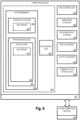
- Fig. 6 and the associated descriptions provide a discussion of a variety of operating environments in which aspects of the disclosure may be practiced.
- the devices and systems illustrated and discussed with respect to Fig. 6 are for purposes of example and illustration and are not limiting of a vast number of computing device configurations that may be utilized for practicing aspects of the disclosure, as described herein.
- embodiments of the disclosure may be practiced in an electrical circuit comprising discrete electronic elements, packaged or integrated electronic chips containing logic gates, a circuit utilizing a microprocessor, or on a single chip containing electronic elements or microprocessors.
- embodiments of the disclosure may be practiced via a system-on-a-chip (SOC) where each or many of the components illustrated in Fig. 6 may be integrated onto a single integrated circuit.
- SOC system-on-a-chip
- Such an SOC device may include one or more processing units, graphics units, communications units, system virtualization units and various application functionality all of which are integrated (or "burned") onto the chip substrate as a single integrated circuit.
- the functionality, described herein, with respect to the capability of client to switch protocols may be operated via application-specific logic integrated with other components of the computing device 600 on the single integrated circuit (chip).
- Embodiments of the disclosure may also be practiced using other technologies capable of performing logical operations such as, for example, AND, OR, and NOT, including but not limited to mechanical, optical, fluidic, and quantum technologies.
- embodiments of the disclosure may be practiced within a general purpose computer or in any other circuits or systems.
- the computing device 600 may also have one or more input device(s) 612 such as a keyboard, a mouse, a pen, a sound or voice input device, a touch or swipe input device, etc.
- the output device(s) 614 such as a display, speakers, a printer, etc. may also be included.
- the aforementioned devices are examples and others may be used.
- the computing device 600 may include one or more communication connections 616 allowing communications with other computing devices 650. Examples of suitable communication connections 616 include, but are not limited to, radio frequency (RF) transmitter, receiver, and/or transceiver circuitry; universal serial bus (USB), parallel, and/or serial ports.
- RF radio frequency
- USB universal serial bus
- Computer readable media may include computer storage media.
- Computer storage media may include volatile and nonvolatile, removable and non-removable media implemented in any method or technology for storage of information, such as computer readable instructions, data structures, or program modules.
- the system memory 604, the removable storage device 609, and the non-removable storage device 610 are all computer storage media examples (e.g., memory storage).
- Computer storage media may include RAM, ROM, electrically erasable read-only memory (EEPROM), flash memory or other memory technology, CD-ROM, digital versatile disks (DVD) or other optical storage, magnetic cassettes, magnetic tape, magnetic disk storage or other magnetic storage devices, or any other article of manufacture which can be used to store information and which can be accessed by the computing device 600. Any such computer storage media may be part of the computing device 600.
- Computer storage media does not include a carrier wave or other propagated or modulated data signal.
- Communication media may be embodied by computer readable instructions, data structures, program modules, or other data in a modulated data signal, such as a carrier wave or other transport mechanism, and includes any information delivery media.
- modulated data signal may describe a signal that has one or more characteristics set or changed in such a manner as to encode information in the signal.
- communication media may include wired media such as a wired network or direct-wired connection, and wireless media such as acoustic, radio frequency (RF), infrared, and other wireless media.
- RF radio frequency
Landscapes
- Engineering & Computer Science (AREA)
- Theoretical Computer Science (AREA)
- Physics & Mathematics (AREA)
- General Engineering & Computer Science (AREA)
- General Physics & Mathematics (AREA)
- Human Computer Interaction (AREA)
- Mathematical Physics (AREA)
- Information Retrieval, Db Structures And Fs Structures Therefor (AREA)
- Storage Device Security (AREA)
Claims (15)
- Verfahren zum Zugreifen auf Blöcke eines Solid-State-Laufwerks (200), wobei das Verfahren umfasst:Empfangen einer Startposition, welche einen ersten Block (312) einer zusammenhängenden Blockregion (310) innerhalb eines Namensraums (300) des Solid-State-Laufwerks (200) identifiziert, auf welchen gemäß eines einzelnen Ein-/AusgabeVorgangs zugegriffen werden soll, wobei der Namensraum (300) zwei Dimensionen eines logischen Adressraums mit jeweiligen Indizes zum Indizieren von Blöcken innerhalb einer entsprechenden Dimension des logischen Adressraums umfasst;Empfangen einer ersten Dimensionskennung, welche eine Größe der zusammenhängenden Blockregion (310) in einer ersten Dimension des Namensraums (300) identifiziert, und einer zweiten Dimensionskennung, welche eine Größe der zusammenhängenden Blockregion (310) in einer zweiten Dimension des Namensraums (300) identifiziert; undZugreifen auf Blöcke der zusammenhängenden Blockregion (310) als Reaktion auf den einzelnen Ein-/Ausgabe-Vorgang gemäß der Startposition, der ersten Dimensionskennung und der zweiten Dimensionskennung; unddadurch gekennzeichnet, dass das Verfahren weiter umfasst:Empfangen einer Zugriffsreihenfolge, welche entweder die erste Dimension oder die zweite Dimension priorisiert; undZugreifen auf jeden der Blöcke der zusammenhängenden Blockregion (310) in der priorisierten Dimension von dem ersten Block (312) aus, bevor auf die verbleibenden Blöcke der zusammenhängenden Blockregion (310) zugegriffen wird.
- Verfahren nach Anspruch 1, weiter umfassend:
Abbilden des logischen Adressraums auf einen physischen Adressraum der Blöcke. - Verfahren nach Anspruch 1, wobei die Startposition ein 2-Tupel mit einem ersten Index, welcher eine Position des ersten Blocks (312) in der ersten Dimension identifiziert, und einem zweiten Index umfasst, welcher die Position des ersten Blocks (312) in der zweiten Dimension identifiziert.
- Verfahren nach Anspruch 1, wobei die Startposition einen einzelnen Wert umfasst, welcher eine Position des ersten Blocks (312) identifiziert, wobei das Verfahren weiter Abbilden des einzelnen Werts auf die erste Dimension unter Verwendung einer Ganzzahldivisionsoperation und auf die zweite Dimension unter Verwendung einer Moduloperation umfasst.
- Verfahren nach Anspruch 1, wobei der einzelne Ein-/Ausgabe-Vorgang eines von Lesen von Daten aus jedem Block der zusammenhängenden Blockregion (310) oder Schreiben von Daten aus jedem Block der zusammenhängenden Blockregion (310) umfasst.
- Verfahren nach Anspruch 5, wobei das Verfahren weiter umfasst:Empfangen einer Anforderung zur Identifizierung des Namensraums (300); undBereitstellen einer Antwort auf die Anforderung zur Identifizierung, welche eine maximale Größe des Namensraums (300) in der ersten Dimension und eine maximale Größe des Namensraums (300) in der zweiten Dimension angibt.
- Verfahren nach Anspruch 1, wobei der einzelne Ein-/Ausgabe-Vorgang Formatieren von zumindest einem Teil des Solid-State-Laufwerks (200) umfasst, um den Namensraum (300) mit der Größe der zusammenhängenden Blockregion (310) zu konfigurieren.
- Verfahren nach Anspruch 7, wobei sich die Größe der zusammenhängenden Blockregion (310) von einer vorherigen Konfiguration des Namensraums (300) unterscheidet.
- Verfahren nach Anspruch 1, wobei der Namensraum (300) drei Dimensionen umfasst, wobei das Verfahren weiter Empfangen einer dritten Dimensionskennung umfasst, welche eine Größe der zusammenhängenden Blockregion (310) in einer dritten Dimension des Namensraums (300) identifiziert;
wobei Zugreifen auf Blöcke der zusammenhängenden Blockregion (310) Zugreifen auf die Blöcke der zusammenhängenden Blockregion (310) gemäß der Startposition, der ersten Dimensionskennung, der zweiten Dimensionskennung und der dritten Dimensionskennung umfasst. - System zum Zugreifen auf Blöcke eines Solid-State-Laufwerks (200), wobei das System umfasst: einen oder mehrere NAND-Speicherchips (210, 220, 230, 240) zur Datenspeicherung;eine Laufwerkspeichersteuereinheit, welche dazu konfiguriert ist, auf den einen oder die mehreren NAND-Speicherchips (210, 220, 230, 240) zuzugreifen und den einen oder die mehreren NAND-Speicherchips (210, 220, 230, 240) mit einem Namensraum (300) zu konfigurieren, welcher zwei Dimensionen eines logischen Adressraums mit jeweiligen Indizes zum Indizieren von Blöcken innerhalb einer entsprechenden Dimension des logischen Adressraums umfasst;wobei die Laufwerkspeichersteuereinheit dazu konfiguriert ist:eine Startposition zu empfangen, welche einen ersten Block (312) einer zusammenhängenden Blockregion (310) innerhalb des Namensraums (300) identifiziert, auf welchen gemäß einem einzelnen Ein-/Ausgabe-Vorgang zugegriffen werden soll;eine erste Dimensionskennung, welche eine Größe der zusammenhängenden Blockregion (310) in einer ersten Dimension des Namensraums (300) identifiziert, und eine zweite Dimensionskennung, welche eine Größe der zusammenhängenden Blockregion (310) in einer zweiten Dimension des Namensraums (300) identifiziert, zu empfangen; undals Reaktion auf den einzelnen Ein-/Ausgabe-Vorgang gemäß der Startposition, der ersten Dimensionskennung und der zweiten Dimensionskennung auf Blöcke der zusammenhängenden Blockregion (310) zuzugreifen; unddadurch gekennzeichnet, dass die Laufwerkspeichersteuereinheit weiter dazu konfiguriert ist:eine Zugriffsreihenfolge zu empfangen, welche entweder die erste Dimension oder die zweite Dimension priorisiert; undauf jeden der Blöcke der zusammenhängenden Blockregion (310) in der priorisierten Dimension von dem ersten Block (312) aus zuzugreifen, bevor auf die verbleibenden Blöcke der zusammenhängenden Blockregion (310) zugegriffen wird.
- System nach Anspruch 10, wobei die Laufwerkspeichersteuereinheit konfiguriert ist zum:
Abbilden des logischen Adressraums auf einen physischen Adressraum der Blöcke. - System nach Anspruch 10, wobei die Startposition ein 2-Tupel mit einem ersten Index, welcher eine Position des ersten Blocks (312) in der ersten Dimension identifiziert, und einem zweiten Index umfasst, welcher die Position des ersten Blocks (312) in der zweiten Dimension identifiziert.
- System nach Anspruch 10, wobei der einzelne Ein-/Ausgabe-Vorgang eines von Lesen von Daten aus jedem Block der zusammenhängenden Blockregion (310) oder Schreiben von Daten aus jedem Block der zusammenhängenden Blockregion (310) umfasst.
- System nach Anspruch 13, wobei die Laufwerkspeichersteuereinheit dazu konfiguriert ist:eine Anforderung zur Identifizierung des Namensraums (300) zu empfangen; undeine Antwort auf die Anforderung zur Identifizierung bereitzustellen, welche eine maximale Größe des Namensraums in der ersten Dimension und eine maximale Größe des Namensraums (300) in der zweiten Dimension angibt.
- Nichtflüchtiges computerlesbares Speichermedium, welches Anweisungen umfasst, welche von einem oder mehreren Prozessoren ausgeführt werden können, welche, wenn sie von dem einem oder den mehreren Prozessoren ausgeführt werden, bewirken, dass der eine oder die mehreren Prozessoren das Verfahren nach einem der Ansprüche 1-9 durchführen.
Applications Claiming Priority (1)
| Application Number | Priority Date | Filing Date | Title |
|---|---|---|---|
| US18/108,351 US12271612B2 (en) | 2023-02-10 | 2023-02-10 | Multi-dimensional solid state drive block access |
Publications (2)
| Publication Number | Publication Date |
|---|---|
| EP4414822A1 EP4414822A1 (de) | 2024-08-14 |
| EP4414822B1 true EP4414822B1 (de) | 2025-07-09 |
Family
ID=86767948
Family Applications (1)
| Application Number | Title | Priority Date | Filing Date |
|---|---|---|---|
| EP24155617.4A Active EP4414822B1 (de) | 2023-02-10 | 2024-02-02 | Mehrdimensionaler festkörperantriebsblockzugriff |
Country Status (3)
| Country | Link |
|---|---|
| US (1) | US12271612B2 (de) |
| EP (1) | EP4414822B1 (de) |
| CN (1) | CN118484133A (de) |
Family Cites Families (5)
| Publication number | Priority date | Publication date | Assignee | Title |
|---|---|---|---|---|
| IL235729A (en) * | 2014-11-17 | 2017-06-29 | Kaluzhny Uri | A device and method for securely storing information |
| US20180239697A1 (en) | 2017-02-22 | 2018-08-23 | CNEXLABS, Inc. a Delaware Corporation | Method and apparatus for providing multi-namespace using mapping memory |
| US10503404B2 (en) | 2017-10-23 | 2019-12-10 | Micron Technology, Inc. | Namespace management in non-volatile memory devices |
| US11823771B2 (en) * | 2020-01-30 | 2023-11-21 | Stmicroelectronics S.R.L. | Streaming access memory device, system and method |
| CN114691020B (zh) | 2020-12-30 | 2026-01-27 | 上海曼卜信息科技有限公司 | 基于zns标准提供数据压缩存储设备及其方法 |
-
2023
- 2023-02-10 US US18/108,351 patent/US12271612B2/en active Active
-
2024
- 2024-02-02 EP EP24155617.4A patent/EP4414822B1/de active Active
- 2024-02-05 CN CN202410164608.1A patent/CN118484133A/zh active Pending
Also Published As
| Publication number | Publication date |
|---|---|
| CN118484133A (zh) | 2024-08-13 |
| US20230195345A1 (en) | 2023-06-22 |
| EP4414822A1 (de) | 2024-08-14 |
| US12271612B2 (en) | 2025-04-08 |
Similar Documents
| Publication | Publication Date | Title |
|---|---|---|
| US12216931B1 (en) | Techniques for directed data migration | |
| US10761977B2 (en) | Memory system and non-transitory computer readable recording medium | |
| US8700881B2 (en) | Controller, data storage device and data storage system having the controller, and data processing method | |
| US8762627B2 (en) | Memory logical defragmentation during garbage collection | |
| US11556466B2 (en) | Logical-to-physical data structures | |
| US11010079B2 (en) | Concept for storing file system metadata within solid-stage storage devices | |
| US10606744B2 (en) | Method for accessing flash memory module and associated flash memory controller and electronic device | |
| US11868246B2 (en) | Memory system and non-transitory computer readable recording medium | |
| US20190146926A1 (en) | Storage device and operating method of storage device | |
| US12498887B2 (en) | File system improvements for zoned storage device operations | |
| US11372774B2 (en) | Method and system for a solid state drive with on-chip memory integration | |
| US12072797B2 (en) | Memory system and non-transitory computer readable recording medium | |
| EP4414822B1 (de) | Mehrdimensionaler festkörperantriebsblockzugriff | |
| CN115079957A (zh) | 请求处理方法、装置、控制器、设备及存储介质 | |
| TWI835027B (zh) | 更新主機與閃存位址對照表的方法及電腦程式產品及裝置 | |
| CN119225629A (zh) | 一种数据存储方法和相关设备 |
Legal Events
| Date | Code | Title | Description |
|---|---|---|---|
| PUAI | Public reference made under article 153(3) epc to a published international application that has entered the european phase |
Free format text: ORIGINAL CODE: 0009012 |
|
| STAA | Information on the status of an ep patent application or granted ep patent |
Free format text: STATUS: REQUEST FOR EXAMINATION WAS MADE |
|
| 17P | Request for examination filed |
Effective date: 20240202 |
|
| AK | Designated contracting states |
Kind code of ref document: A1 Designated state(s): AL AT BE BG CH CY CZ DE DK EE ES FI FR GB GR HR HU IE IS IT LI LT LU LV MC ME MK MT NL NO PL PT RO RS SE SI SK SM TR |
|
| GRAP | Despatch of communication of intention to grant a patent |
Free format text: ORIGINAL CODE: EPIDOSNIGR1 |
|
| STAA | Information on the status of an ep patent application or granted ep patent |
Free format text: STATUS: GRANT OF PATENT IS INTENDED |
|
| RIC1 | Information provided on ipc code assigned before grant |
Ipc: G06F 12/02 20060101ALI20250226BHEP Ipc: G06F 3/06 20060101AFI20250226BHEP |
|
| INTG | Intention to grant announced |
Effective date: 20250326 |
|
| GRAS | Grant fee paid |
Free format text: ORIGINAL CODE: EPIDOSNIGR3 |
|
| GRAA | (expected) grant |
Free format text: ORIGINAL CODE: 0009210 |
|
| STAA | Information on the status of an ep patent application or granted ep patent |
Free format text: STATUS: THE PATENT HAS BEEN GRANTED |
|
| AK | Designated contracting states |
Kind code of ref document: B1 Designated state(s): AL AT BE BG CH CY CZ DE DK EE ES FI FR GB GR HR HU IE IS IT LI LT LU LV MC ME MK MT NL NO PL PT RO RS SE SI SK SM TR |
|
| REG | Reference to a national code |
Ref country code: GB Ref legal event code: FG4D |
|
| REG | Reference to a national code |
Ref country code: CH Ref legal event code: EP |
|
| REG | Reference to a national code |
Ref country code: IE Ref legal event code: FG4D |
|
| REG | Reference to a national code |
Ref country code: DE Ref legal event code: R096 Ref document number: 602024000280 Country of ref document: DE |
|
| REG | Reference to a national code |
Ref country code: NL Ref legal event code: MP Effective date: 20250709 |
|
| PG25 | Lapsed in a contracting state [announced via postgrant information from national office to epo] |
Ref country code: PT Free format text: LAPSE BECAUSE OF FAILURE TO SUBMIT A TRANSLATION OF THE DESCRIPTION OR TO PAY THE FEE WITHIN THE PRESCRIBED TIME-LIMIT Effective date: 20251110 |
|
| PG25 | Lapsed in a contracting state [announced via postgrant information from national office to epo] |
Ref country code: NL Free format text: LAPSE BECAUSE OF FAILURE TO SUBMIT A TRANSLATION OF THE DESCRIPTION OR TO PAY THE FEE WITHIN THE PRESCRIBED TIME-LIMIT Effective date: 20250709 |
|
| REG | Reference to a national code |
Ref country code: AT Ref legal event code: MK05 Ref document number: 1812444 Country of ref document: AT Kind code of ref document: T Effective date: 20250709 |
|
| PG25 | Lapsed in a contracting state [announced via postgrant information from national office to epo] |
Ref country code: IS Free format text: LAPSE BECAUSE OF FAILURE TO SUBMIT A TRANSLATION OF THE DESCRIPTION OR TO PAY THE FEE WITHIN THE PRESCRIBED TIME-LIMIT Effective date: 20251109 |
|
| PG25 | Lapsed in a contracting state [announced via postgrant information from national office to epo] |
Ref country code: NO Free format text: LAPSE BECAUSE OF FAILURE TO SUBMIT A TRANSLATION OF THE DESCRIPTION OR TO PAY THE FEE WITHIN THE PRESCRIBED TIME-LIMIT Effective date: 20251009 |
|
| REG | Reference to a national code |
Ref country code: LT Ref legal event code: MG9D |
|
| PG25 | Lapsed in a contracting state [announced via postgrant information from national office to epo] |
Ref country code: AT Free format text: LAPSE BECAUSE OF FAILURE TO SUBMIT A TRANSLATION OF THE DESCRIPTION OR TO PAY THE FEE WITHIN THE PRESCRIBED TIME-LIMIT Effective date: 20250709 |
|
| PG25 | Lapsed in a contracting state [announced via postgrant information from national office to epo] |
Ref country code: FI Free format text: LAPSE BECAUSE OF FAILURE TO SUBMIT A TRANSLATION OF THE DESCRIPTION OR TO PAY THE FEE WITHIN THE PRESCRIBED TIME-LIMIT Effective date: 20250709 |
|
| PG25 | Lapsed in a contracting state [announced via postgrant information from national office to epo] |
Ref country code: HR Free format text: LAPSE BECAUSE OF FAILURE TO SUBMIT A TRANSLATION OF THE DESCRIPTION OR TO PAY THE FEE WITHIN THE PRESCRIBED TIME-LIMIT Effective date: 20250709 |
|
| PG25 | Lapsed in a contracting state [announced via postgrant information from national office to epo] |
Ref country code: GR Free format text: LAPSE BECAUSE OF FAILURE TO SUBMIT A TRANSLATION OF THE DESCRIPTION OR TO PAY THE FEE WITHIN THE PRESCRIBED TIME-LIMIT Effective date: 20251010 |
|
| PG25 | Lapsed in a contracting state [announced via postgrant information from national office to epo] |
Ref country code: SE Free format text: LAPSE BECAUSE OF FAILURE TO SUBMIT A TRANSLATION OF THE DESCRIPTION OR TO PAY THE FEE WITHIN THE PRESCRIBED TIME-LIMIT Effective date: 20250709 |
|
| PG25 | Lapsed in a contracting state [announced via postgrant information from national office to epo] |
Ref country code: LV Free format text: LAPSE BECAUSE OF FAILURE TO SUBMIT A TRANSLATION OF THE DESCRIPTION OR TO PAY THE FEE WITHIN THE PRESCRIBED TIME-LIMIT Effective date: 20250709 |
|
| PG25 | Lapsed in a contracting state [announced via postgrant information from national office to epo] |
Ref country code: BG Free format text: LAPSE BECAUSE OF FAILURE TO SUBMIT A TRANSLATION OF THE DESCRIPTION OR TO PAY THE FEE WITHIN THE PRESCRIBED TIME-LIMIT Effective date: 20250709 Ref country code: PL Free format text: LAPSE BECAUSE OF FAILURE TO SUBMIT A TRANSLATION OF THE DESCRIPTION OR TO PAY THE FEE WITHIN THE PRESCRIBED TIME-LIMIT Effective date: 20250709 |
|
| PG25 | Lapsed in a contracting state [announced via postgrant information from national office to epo] |
Ref country code: RS Free format text: LAPSE BECAUSE OF FAILURE TO SUBMIT A TRANSLATION OF THE DESCRIPTION OR TO PAY THE FEE WITHIN THE PRESCRIBED TIME-LIMIT Effective date: 20251009 |
|
| PG25 | Lapsed in a contracting state [announced via postgrant information from national office to epo] |
Ref country code: ES Free format text: LAPSE BECAUSE OF FAILURE TO SUBMIT A TRANSLATION OF THE DESCRIPTION OR TO PAY THE FEE WITHIN THE PRESCRIBED TIME-LIMIT Effective date: 20250709 |
|
| PG25 | Lapsed in a contracting state [announced via postgrant information from national office to epo] |
Ref country code: SM Free format text: LAPSE BECAUSE OF FAILURE TO SUBMIT A TRANSLATION OF THE DESCRIPTION OR TO PAY THE FEE WITHIN THE PRESCRIBED TIME-LIMIT Effective date: 20250709 |
|
| PG25 | Lapsed in a contracting state [announced via postgrant information from national office to epo] |
Ref country code: DK Free format text: LAPSE BECAUSE OF FAILURE TO SUBMIT A TRANSLATION OF THE DESCRIPTION OR TO PAY THE FEE WITHIN THE PRESCRIBED TIME-LIMIT Effective date: 20250709 |
|
| PGFP | Annual fee paid to national office [announced via postgrant information from national office to epo] |
Ref country code: DE Payment date: 20260217 Year of fee payment: 3 |
|
| PG25 | Lapsed in a contracting state [announced via postgrant information from national office to epo] |
Ref country code: IT Free format text: LAPSE BECAUSE OF FAILURE TO SUBMIT A TRANSLATION OF THE DESCRIPTION OR TO PAY THE FEE WITHIN THE PRESCRIBED TIME-LIMIT Effective date: 20250709 |
|
| PGFP | Annual fee paid to national office [announced via postgrant information from national office to epo] |
Ref country code: FR Payment date: 20260119 Year of fee payment: 3 |
|
| PG25 | Lapsed in a contracting state [announced via postgrant information from national office to epo] |
Ref country code: CZ Free format text: LAPSE BECAUSE OF FAILURE TO SUBMIT A TRANSLATION OF THE DESCRIPTION OR TO PAY THE FEE WITHIN THE PRESCRIBED TIME-LIMIT Effective date: 20250709 |
|
| PG25 | Lapsed in a contracting state [announced via postgrant information from national office to epo] |
Ref country code: SK Free format text: LAPSE BECAUSE OF FAILURE TO SUBMIT A TRANSLATION OF THE DESCRIPTION OR TO PAY THE FEE WITHIN THE PRESCRIBED TIME-LIMIT Effective date: 20250709 Ref country code: EE Free format text: LAPSE BECAUSE OF FAILURE TO SUBMIT A TRANSLATION OF THE DESCRIPTION OR TO PAY THE FEE WITHIN THE PRESCRIBED TIME-LIMIT Effective date: 20250709 |