EP4412422A1 - Semiconductor structure and method for manufacturing semiconductor structure - Google Patents
Semiconductor structure and method for manufacturing semiconductor structure Download PDFInfo
- Publication number
- EP4412422A1 EP4412422A1 EP22884864.4A EP22884864A EP4412422A1 EP 4412422 A1 EP4412422 A1 EP 4412422A1 EP 22884864 A EP22884864 A EP 22884864A EP 4412422 A1 EP4412422 A1 EP 4412422A1
- Authority
- EP
- European Patent Office
- Prior art keywords
- conductive layer
- trench
- semiconductor structure
- substrate
- conductive
- Prior art date
- Legal status (The legal status is an assumption and is not a legal conclusion. Google has not performed a legal analysis and makes no representation as to the accuracy of the status listed.)
- Pending
Links
Images






Classifications
-
- H—ELECTRICITY
- H10—SEMICONDUCTOR DEVICES; ELECTRIC SOLID-STATE DEVICES NOT OTHERWISE PROVIDED FOR
- H10B—ELECTRONIC MEMORY DEVICES
- H10B12/00—Dynamic random access memory [DRAM] devices
- H10B12/30—DRAM devices comprising one-transistor - one-capacitor [1T-1C] memory cells
- H10B12/34—DRAM devices comprising one-transistor - one-capacitor [1T-1C] memory cells the transistor being at least partially in a trench in the substrate
-
- H—ELECTRICITY
- H10—SEMICONDUCTOR DEVICES; ELECTRIC SOLID-STATE DEVICES NOT OTHERWISE PROVIDED FOR
- H10B—ELECTRONIC MEMORY DEVICES
- H10B12/00—Dynamic random access memory [DRAM] devices
- H10B12/01—Manufacture or treatment
- H10B12/02—Manufacture or treatment for one transistor one-capacitor [1T-1C] memory cells
- H10B12/05—Making the transistor
- H10B12/053—Making the transistor the transistor being at least partially in a trench in the substrate
-
- H—ELECTRICITY
- H10—SEMICONDUCTOR DEVICES; ELECTRIC SOLID-STATE DEVICES NOT OTHERWISE PROVIDED FOR
- H10W—GENERIC PACKAGES, INTERCONNECTIONS, CONNECTORS OR OTHER CONSTRUCTIONAL DETAILS OF DEVICES COVERED BY CLASS H10
- H10W10/00—Isolation regions in semiconductor bodies between components of integrated devices
- H10W10/01—Manufacture or treatment
- H10W10/011—Manufacture or treatment of isolation regions comprising dielectric materials
-
- H—ELECTRICITY
- H10—SEMICONDUCTOR DEVICES; ELECTRIC SOLID-STATE DEVICES NOT OTHERWISE PROVIDED FOR
- H10W—GENERIC PACKAGES, INTERCONNECTIONS, CONNECTORS OR OTHER CONSTRUCTIONAL DETAILS OF DEVICES COVERED BY CLASS H10
- H10W10/00—Isolation regions in semiconductor bodies between components of integrated devices
- H10W10/10—Isolation regions comprising dielectric materials
Definitions
- the present disclosure relates to the technical field of semiconductors, and in particular to a semiconductor structure and a manufacturing method thereof.
- DRAM dynamic random access memory
- the present disclosure provides a semiconductor structure and a manufacturing method thereof, to improve the performance of the semiconductor structure.
- the present disclosure provides a semiconductor structure, including:
- the conductive portion contacts the substrate.
- a voltage of the conductive portion and a voltage of the substrate are a negative voltage.
- the conductive portion comprises: a first conductive layer, a part of the first conductive layer being located in the isolation structure.
- the first conductive layer contacts the substrate; and a material of the first conductive layer comprises polycrystalline silicon.
- the conductive portion further comprises: a second conductive layer, contacting the substrate, the first conductive layer being located on an upper surface of the second conductive layer.
- a material of the first conductive layer comprises a metal material
- a material of the second conductive layer comprises metal silicide
- a bottom of the first conductive layer is located in the second conductive layer.
- the word line is a buried word line.
- the isolation structure is a shallow trench isolation structure.
- the semiconductor structure further comprising:
- the conductive portion is located below the word line, and insulated from the word line.
- a height of the conductive portion is less than a distance between the conductive portion and the word line.
- the present disclosure provides a method of manufacturing a semiconductor structure, including:
- forming a conductive portion comprises:
- polycrystalline silicon is deposited in the trench to form the first conductive layer.
- forming a conductive portion comprises:
- a first metal material is deposited in the substrate and thermally treated to form metal silicide, the metal silicide serving as the second conductive layer; and a second metal material is formed on the metal silicide, the second metal material serving as the first conductive layer.
- forming a first conductive layer further comprising: forming a third metal material on a wall of the first insulating layer, wherein the first conductive layer is formed in the third metal material.
- the substrate is provided with a plurality of active regions, and the isolation structure is provided between the active regions;
- the semiconductor structure in the embodiment of the present disclosure includes the substrate, the isolation structure, the WL and the conductive portion.
- the conductive portion at the bottom of the isolation structure when the WL is activated, the conductive portion at the bottom of the isolation structure repels surface electrons to block the leakage path, thereby preventing the electric leakage of the semiconductor structure and improving the performance of the semiconductor structure.
- the semiconductor structure includes: a substrate 10; an isolation structure 20, formed in the substrate 10; a WL 30, a part of the WL 30 being located in the isolation structure 20; and a conductive portion 40, located at a bottom of the isolation structure 20, and configured to repel electrons.
- the semiconductor structure provided by the embodiment of the present disclosure includes the substrate 10, the isolation structure 20, the WL 30 and the conductive portion 40.
- the conductive portion 40 at the bottom of the isolation structure 20 repels surface electrons to block the leakage path, thereby preventing the electric leakage of the semiconductor structure and improving the performance of the semiconductor structure.
- the isolation structure 20 is made deep enough to prevent conduction of electrons at two sides of the isolation structure 20.
- the conductive portion 40 repels neighboring electrons to prevent the conduction of electrons at two sides of the isolation structure 20. Therefore, the depth of the isolation structure 20 can be decreased appropriately in the embodiment. Certainly, when the isolation structure 20 is deep enough, the leakage path can be better blocked in combination with the conductive portion 40 at the bottom of the isolation structure 20.
- the substrate 10 may be a p-type silicon substrate, an n-type silicon substrate, a silicon-germanium substrate, etc.
- the conductive portion 40 contacts the substrate 10 to implement electrical connection between the conductive portion 40 and the substrate 10.
- the conductive portion 40 can repel the neighboring electrons to block the leakage path.
- both the conductive portion 40 and the substrate 10 have a negative voltage, and negative electrons are adsorbed to the WL 30 and the surface of the isolation structure 20.
- the conductive portion 40 and the substrate 10 can repel the neighboring electrons to prevent the conduction of electrons at two sides of the isolation structure 20 and block the leakage path.
- the conductive portion 40 includes: a first conductive layer 41. With a part located in the isolation structure 20, the first conductive layer 41 is electrically connected to the substrate 10, ensuring that the conductive portion 40 has the negative voltage to repel the neighboring negative electrons, preventing the conduction of electrons at two sides of the isolation structure 20 and blocking the leakage path.
- the first conductive layer 41 may be directly formed on the substrate 10 to implement contact between the first conductive layer 41 and the substrate 10, ensuring that both the conductive portion 40 and the substrate 10 have the negative voltage to repel the neighboring negative electrons, preventing the conduction of electrons at two sides of the isolation structure 20 and blocking the leakage path.
- a material of the first conductive layer 41 includes polycrystalline silicon. By directly forming the polycrystalline silicon on the substrate 10, not only both the conductive portion 40 and the substrate 10 have the negative voltage, but the polycrystalline silicon can also be formed on the substrate 10 conveniently.
- the first conductive layer 41 may be 20-30 nm high.
- the material of the first conductive layer 41 may be a metal material, such as tungsten (W), tungsten nitride (WN), titanium (Ti), titanium nitride (TiN), molybdenum (Mo), cobalt (Co), nickel (Ni), copper (Cu) or aluminum (Al).
- a bottom end of the first conductive layer 41 may be flush with a bottom end of the isolation structure 20, such that the first conductive layer 41 may be directly formed in the trench 11 of the substrate 10.
- the bottom end of the first conductive layer 41 may be lower than the bottom end of the isolation structure 20, namely the bottom of the first conductive layer 41 is located in the substrate 10 by forming a recess in a bottom wall of the trench 11 and forming the bottom of the first conductive layer 41 in the recess.
- the conductive portion 40 further includes: a second conductive layer 42.
- the second conductive layer 42 contacts the substrate 10.
- the first conductive layer 41 is located on an upper surface of the second conductive layer 42 to implement contact between the first conductive layer 41 and the second conductive layer 42.
- the conductive portion 40 includes a first conductive layer 41 and a second conductive layer 42.
- the second conductive layer 42 is located in the substrate 10, and electrically connected to the substrate 10, and the first conductive layer 41 is electrically connected to the substrate 10 through the second conductive layer 42, such that both the conductive portion 40 and the substrate 10 have the negative voltage and can repel the neighboring negative electrons, thereby preventing the conduction of electrons at two sides of the isolation structure 20 and blocking the leakage path.
- a bottom of the first conductive layer 41 is located in the second conductive layer 42 to implement more stable conduction between the first conductive layer 41 and the second conductive layer 42.
- a bottom end of the first conductive layer 41 abuts against a top end of the second conductive layer 42.
- a material of the first conductive layer 41 includes a metal material, while a material of the second conductive layer 42 includes metal silicide.
- the first conductive layer 41 is electrically connected to the substrate 10, and the second conductive layer 42 may be formed in the substrate 10.
- the first conductive layer 41 may be 20-30 nm high, while the second conductive layer 42 may be 10-20 nm high.
- the metal material may include, but is not limited to: tungsten (W), tungsten nitride (WN), titanium (Ti), titanium nitride (TiN), molybdenum (Mo), cobalt (Co), nickel (Ni), copper (Cu) or aluminum (Al).
- the metal silicide may include, but is not limited to: at least one of nickel silicide, platinum silicide and cobalt silicide.
- the isolation structure 20 is a shallow trench isolation (STI) structure.
- STI shallow trench isolation
- the semiconductor structure further includes: a first contact plug 50, and a second contact plug 51.
- the first contact plug 50 and the second contact plug 51 are located at two sides of the WL 30. Both the first contact plug 50 and the second contact plug 51 are a capacitance contact plug.
- the first contact plug 50 and the second contact plug 51 are configured to connect two capacitor structures.
- the first contact plug 50 and the second contact plug 51 are connected to the electrons at two sides of the isolation structure 20. While the electrons at two sides of the isolation structure 20 are connected, the first contact plug 50 and the second contact plug 51 are also connected to cause the electric leakage between the two capacitor structures.
- the conductive portion 40 is formed at the bottom of the isolation structure 20 and the conductive portion 40 repels the neighboring electrons, the conduction of electrons at two sides of the isolation structure 20 can be blocked to prevent the electric leakage between the two capacitor structures.
- the semiconductor structure may further include a third contact plug 52, as shown in FIG. 1 and FIG. 3 .
- a third contact plug 52 may be a plurality of the first contact plugs 50, a plurality of the second contact plugs 51 and a plurality of the third contact plugs 52, which is not limited herein and may be determined according to actual needs.
- the conductive portion 40 is located below the WL 30, and insulated from the WL 30. When the WL 30 is activated, the conductive portion 40 repels the neighboring electrons to prevent the conduction of electrons at two sides of the isolation structure 20.
- a height of the conductive portion 40 is less than a distance between the conductive portion 40 and the WL 30. That is, while the conductive portion 40 blocks the leakage path, the conductive portion 40 can be made as small as possible.
- an isolation layer 31 is formed in the isolation structure 20.
- the isolation layer 31 is located on the WL 30.
- the isolation layer 31 can protect the WL 30.
- the isolation layer 31 may include nitride or silicon oxide.
- an insulating layer 12 is formed on an upper surface of the substrate 10 to cover the upper surface of the substrate 10.
- the isolation structure 20 in the substrate 10 is integrally formed, and thus an insulating material formed into the isolation structure 20 covers the upper surface of the substrate 10.
- the insulating layer 12 covers the insulating material.
- the insulating layer 12 may include nitride or silicon oxide.
- the WL 30 is a buried WL.
- a material of the WL 30 includes one or any combination of tungsten, titanium, nickel, aluminum, platinum, titanium nitride and other conductive materials.
- an isolation layer 31 is further formed in a WL trench 21. The isolation layer 31 is located on the WL 30. The isolation layer 31 can protect the WL 30. Upon formation of the isolation layer 31, the isolation layer 31 may be planarized with dry etching or chemical mechanical polishing (CMP).
- an isolation structure 20 is formed in the substrate 10.
- the isolation structure 20 isolates a plurality of active regions 13.
- the WL 30 is located in the isolation structure 20 and in the active region 13.
- the conductive portion 40 may be provided below the WL 30 in the isolation structure 20. In some embodiments, the conductive portion 40 may not be provided below one or more WLs 30 among a plurality of WLs 30 in the isolation structure 20.
- two capacitance contact plugs such as the first contact plug 50 and the second contact plug 51
- the conductive portion 40 is provided below the corresponding WL 30 in the isolation structure 20 to prevent the electric leakage between the two capacitor structures.
- the WL 30 may include a plurality of protrusive structures that may be located in the isolation structure 20 and the active region 13.
- the protrusive structures may have a same height, and may also have different heights.
- An embodiment of the present disclosure further provides a method of manufacturing a semiconductor structure. As shown in FIG. 5 , the method of manufacturing a semiconductor structure includes the following steps:
- the trench 11 is formed in the substrate 10
- the isolation structure 20 is formed in the trench 11
- the conductive portion 40 is formed at the bottom of the isolation structure 20
- the WL 30 is formed in the WL trench 21 of the isolation structure 20.
- the conductive portion 40 at the bottom of the isolation structure 20 can repel surface electrons to block the leakage path, thereby preventing the electric leakage of the semiconductor structure and improving the performance of the semiconductor structure.
- the trench 11 is formed in the substrate 10, and a plurality of active regions 13 are isolated in the trench 11.
- the trench 11 may be formed by STI.
- an insulating layer 12 is formed on an upper surface of the substrate 10.
- a mask structure may cover the insulating layer 12, and a pattern corresponding to the trench 11 may be formed on the insulating layer 12, thereby etching a through hole in the insulating layer 12 and forming a recess in the substrate 10 to form the trench 11, as shown in FIG. 6 and FIG. 7 .
- the conductive portion 40 before a part of the conductive portion 40 is formed in the isolation structure 20, the conductive portion is formed in the trench 11 and contacts the substrate 10, which can ensure that both the conductive portion 40 and the substrate 10 has a negative voltage, and the conductive portion 40 and the substrate 10 repel neighboring electrons, thereby preventing the electron conduction at two sides of the isolation structure 20 and blocking the leakage path.
- the conductive portion 40 cannot be formed at the bottom of the isolation structure 20, unless the conductive portion 40 is formed before the isolation structure 20 is formed completely.
- a first conductive layer 41 is formed in the trench 11, the first conductive layer 41 serving as the conductive portion 40. Specifically, upon formation of the trench 11, the first conductive layer 41 may be formed at a bottom of the trench 11. The first conductive layer 41 may fill up the bottom of the trench 11. The first conductive layer 41 is etched to expose a bottom sidewall of the trench 11. The isolation structure 20 is filled in the trench 11 to cover the first conductive layer 41. Optionally, a part of the isolation structure 20 is filled in the trench 11, an opening is formed in the isolation structure to expose the substrate 10, and the first conductive layer 41 is formed in the opening. Thereafter, a remaining part of the isolation structure 20 is filled in the trench 11 to cover the first conductive layer 41.
- a second conductive layer 42 is formed in the substrate 10.
- a first conductive layer 41 is formed on the second conductive layer 42.
- a part of the first conductive layer 41 is formed in the trench 11.
- the first conductive layer 41 and the second conductive layer 42 serve as the conductive portion 40.
- a recess may be formed in the substrate 10 through the trench 11.
- a second conductive layer 42 is formed in the recess.
- a first conductive layer 41 is formed at the bottom of the trench 11.
- the first conductive layer 41 may fill up the bottom of the trench 11.
- the first conductive layer 41 is etched to expose a bottom sidewall of the trench 11.
- the isolation structure 20 is filled in the trench 11 to cover the first conductive layer 41.
- a recess may be formed in the substrate 10 through the trench 11.
- a second conductive layer 42 is formed in the recess.
- a part of the isolation structure 20 is filled in the trench 11, an opening is formed in the isolation structure to expose the second conductive layer 42, and the first conductive layer 41 is formed in the opening. Thereafter, a remaining part of the isolation structure 20 is filled in the trench 11 to cover the first conductive layer 41.
- a metal material is deposited in the substrate 10 through the trench 11 and annealed to form the second conductive layer 42.
- the first conductive layer 41 may be formed according to the above two manners.
- the metal material reacts with silicon in the substrate 10 to form the second conductive layer 42.
- the metal material may be deposited by physical vapor deposition (PVD), chemical vapor deposition (CVD) or atomic layer deposition (ALD).
- the metal material may include one or more of nickel, platinum, cobalt and so on.
- annealing is performed to form the second conductive layer 42 upon deposition of the metal material in the substrate 10.
- the annealing may be hightemperature furnace tube propulsion, and may also be rapid thermal annealing (RTA) in the related art.
- the step of forming a conductive portion 40 includes: Form a first conductive layer 41 in the trench 11, the first conductive layer 41 serving as the conductive portion 40.
- a first insulating layer 22 is formed between the first conductive layer 41 and a sidewall of the trench 11 to ensure insulation between the first conductive layer 41 and the sidewall of the trench 11. Therefore, while the conductive portion 40 can repel surface electrons, the first conductive layer 41 cannot be overlarge.
- the first insulating layer 22 is formed in the trench 11, the first insulating layer 22 filling up the trench 11 and covering the insulating layer 12, as shown in FIG. 8 and FIG. 9 .
- the first insulating layer 22 may be nitride or silicon oxide.
- the first insulating layer 22 may be formed with the PVD, the CVD or the ALD.
- An opening 221 is formed in the first insulating layer 22, and the opening 221 exposes the substrate 10, namely the first insulating layer 22 covers a sidewall of the opening 221, as shown in FIG. 10 and FIG. 11 . In some embodiments, there remains a part of the first insulating layer 22 on the insulating layer 12, as shown in FIG. 10 . In some embodiments, the first insulating layer 22 on the insulating layer 12 can be removed completely, as shown in FIG. 11 . The opening 221 may be etched. The opening 221 serves as a part of the trench 11.
- polycrystalline silicon 411 is deposited in the trench 11 to form the first conductive layer 41, namely the polycrystalline silicon 411 serves as the conductive portion 40 to repel the neighboring electrons.
- polycrystalline silicon 411 is deposited in the opening 221, the polycrystalline silicon 411 filling up the opening 221 and covering the insulating layer 12, as shown in FIG. 12A .
- the polycrystalline silicon 411 on the insulating layer 12 and a part of the polycrystalline silicon 411 in the opening 221 are removed by etching.
- the remaining polycrystalline silicon 411 is 20-30 nm high to serve as the conductive portion 40.
- the step of forming a conductive portion 40 includes: Form a second conductive layer 42 on the substrate 10 through the trench 11; and form a first conductive layer 41 on an upper surface of the second conductive layer 42, the first conductive layer 41 and the second conductive layer 42 serving as the conductive portion 40.
- the first conductive layer 41 is formed in the trench 11, and a first insulating layer 22 is formed between the first conductive layer 41 and a sidewall of the trench 11.
- the first conductive layer 41 is electrically connected to the substrate 10 through the second conductive layer 42, such that both the conductive portion 40 and the substrate 10 have the negative voltage, and can repel the neighboring electrons, thereby preventing the conduction of electrons at two sides of the isolation structure 20 and blocking the leakage path.
- a first metal material 421 is deposited in the substrate 10 and thermally treated to form metal silicide, the metal silicide serving as the second conductive layer 42.
- a second metal material 412 is formed on the metal silicide, the second metal material 412 serving as the first conductive layer 41.
- the first conductive layer 41 and the second conductive layer 42 are separately formed by the first metal material 421 and the second metal material 412, and are connected to each other to repel the neighboring electrons, thereby preventing the conduction of electrons at two sides of the isolation structure 20 and blocking the leakage path.
- a first metal material 421 is deposited in the opening 221.
- the first metal material 421 fills up the opening 221, and covers the insulating layer 12.
- the first metal material 421 reacts with the substrate 10 to form the metal silicide.
- the metal silicide serves as the second conductive layer 42, as shown in FIG. 12B .
- the thermal treatment may be performed at 340-450°C.
- the first metal material 421 contacting the substrate 10 and a part of the metal silicide are removed with wet etching to expose the second conductive layer 42, as shown in FIG. 13 .
- the remaining metal silicide may be 10-20 nm high, namely the second conductive layer 42 may be 10-20 nm high.
- a third metal material 422 is formed on a wall of the first insulating layer 22.
- the first conductive layer 41 is formed in the third metal material 422.
- the third metal material 422 protects the first conductive layer 41.
- the third metal material 422 is deposited in the opening 221.
- the third metal material 422 fills up the opening 221, covers the insulating layer 12, and contacts the second conductive layer 42, as shown in FIG. 14 .
- the second metal material 412 may be tungsten.
- the third metal material 422 may be metal nitride, such as the third metal material 422 may be titanium nitride.
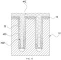
- a recess 4221 is formed in the third metal material 422, and the second metal material 412 is deposited in the recess 4221.
- the second metal material 412 fills up the recess 4221, and covers an upper surface of the third metal material 422, as shown in FIG. 15 .
- the second metal material 412 and the third metal material 422 are etched. There remains a part of the second metal material 412 and a part of the third metal material 422 in the opening 221.
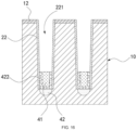
- the remaining second metal material 412 serves as the first conductive layer 41, and the first conductive layer 41 is located in the remaining third meal material 422, as shown in FIG. 16 .
- the remaining second metal material 412 may be 20-30 nm high.
- the conductive portion 40 may include the metal silicide formed by the first metal material 421 and the substrate 10, the second metal material 412 and the third metal material 422.
- the WL trench 21 is formed in the isolation structure 20 and in the active region 13.
- the WL 30 is formed in the WL trench 21 of each of the isolation structure 20 and the active region 13.
- a second insulating layer 24 is formed in the opening 221.
- the second insulating layer 24 fills the exposed opening 221, and covers the insulating layer 12, as shown in FIG. 17 .
- a plurality of the WL trenches 21 are formed in the second insulating layer 24 and the active region 13.
- the WL 30 is formed in the WL trench 21.
- a part of the second insulating layer 24 is removed to expose the opening 221 in the second insulating layer 24, namely the exposed opening 221 serves as the WL trench 21 in the isolation structure 20.
- the WL trench 21 is also formed in the active region 13.
- the first insulating layer 22 and the second insulating layer 24 may serve as the isolation structure 20.
- the WL 30 may include a barrier layer 34, a conductive layer 32 and a third insulating layer 33.
- the barrier layer 34 covers a wall of the WL trench 21.
- the conductive layer 32 is located in the barrier layer 34.
- the third insulating layer 33 covers the barrier layer 34 and the conductive layer 32, as shown in FIG. 18 .
- the barrier layer 34 fills up the WL trench 21, and is etched to make a remaining part of the barrier layer 34 cover the wall of the WL trench 21.
- the conductive layer 32 is filled in the barrier layer 34.
- the conductive layer 32 is etched, such that an upper surface of the conductive layer 32 is flush with an upper surface of the barrier layer 34.
- the third insulating layer 33 is formed at last.
- the barrier layer 34 may include Ta, Ti, Ru, TaN, TiN, RuTa, RuTaN, W or Ir.
- the barrier layer 34 may be formed by any material capable of preventing diffusion of the conductive material layer.
- the conductive layer 32 may be formed by a metal material such as Cu, Al, W or alloy.
- the third insulating layer 33 may be formed by a material including silicon oxide, silicon nitride or a combination thereof.
- the third insulating layer 33 may be formed by SIN, SION or SIO2.
- a fourth insulating layer 211 is formed on a sidewall of the WL trench 21.
- the WL 30 is formed in the fourth insulating layer 211.
- the fourth insulating layer 211 may be formed by a material including silicon oxide, silicon nitride or a combination thereof.
- the fourth insulating layer 211 may be formed by SIN, SION or SIO2.
- the first conductive layer 41 serves as the conductive portion 40
- the second insulating layer 24 is formed on the polycrystalline silicon 411
- the WL trench 21 is formed in each of the isolation structure 20 and the active region 13
- the WL 30 is formed in the WL trench 21 in each of the isolation structure 20 and the active region 13.
- the specific structure and process may refer to those when the first conductive layer 41 and the second conductive layer 42 serves as the conductive portion 40.
- the method of manufacturing a semiconductor structure further includes: Form a first contact plug 50 and a second contact plug 51 at two sides of the WL 30. Both the first contact plug 50 and the second contact plug 51 are a capacitance contact plug. The first contact plug 50 and the second contact plug 51 are configured to connect two capacitor structures.
- the first contact plug 50 and the second contact plug 51 are connected to the electrons at two sides of the isolation structure 20. While the electrons at two sides of the isolation structure 20 are connected, the first contact plug 50 and the second contact plug 51 are also connected to cause the electric leakage between the two capacitor structures.
- the conductive portion 40 is formed at the bottom of the isolation structure 20 and the conductive portion 40 repels the neighboring electrons, the conduction of electrons at two sides of the isolation structure 20 can be blocked to prevent the electric leakage between the two capacitor structures.
- the semiconductor structure formed with the method is provided with the conductive portion 40 at the bottom of the isolation structure 20.
- the conductive portion 40 can repel the electrons, thereby reducing the current leakage of the semiconductor structure and improving the performance of the semiconductor structure.
- the semiconductor structure is applied to the DRAM device with the small size and the high performance.
- the semiconductor structure in the embodiment is obtained through the method of manufacturing a semiconductor structure.
Landscapes
- Engineering & Computer Science (AREA)
- Manufacturing & Machinery (AREA)
- Internal Circuitry In Semiconductor Integrated Circuit Devices (AREA)
- Element Separation (AREA)
Abstract
Description
- The present disclosure claims the priority to
Chinese Patent Application No. 202111242748.9, titled "SEMICONDUCTOR STRUCTURE AND MANUFACTURING METHOD THEREOF", filed on October 25, 2021 - The present disclosure relates to the technical field of semiconductors, and in particular to a semiconductor structure and a manufacturing method thereof.
- With miniaturization of the dynamic random access memory (DRAM), there is an increasingly small transistor size in the storage region to cause serious current leakage and to affect performance of the device.
- The present disclosure provides a semiconductor structure and a manufacturing method thereof, to improve the performance of the semiconductor structure.
- According to a first aspect, the present disclosure provides a semiconductor structure, including:
- a substrate;
- an isolation structure, formed in the substrate;
- a word line (WL), a part of the WL being located in the isolation structure; and
- a conductive portion, located at a bottom of the isolation structure.
- Furthermore, the conductive portion contacts the substrate.
- Furthermore, a voltage of the conductive portion and a voltage of the substrate are a negative voltage.
- Furthermore, the conductive portion comprises:
a first conductive layer, a part of the first conductive layer being located in the isolation structure. - Furthermore, the first conductive layer contacts the substrate; and
a material of the first conductive layer comprises polycrystalline silicon. - Furthermore, the conductive portion further comprises:
a second conductive layer, contacting the substrate, the first conductive layer being located on an upper surface of the second conductive layer. - Furthermore, a material of the first conductive layer comprises a metal material, while a material of the second conductive layer comprises metal silicide.
- Furthermore, a bottom of the first conductive layer is located in the second conductive layer.
- Furthermore, the word line is a buried word line.
- Furthermore, the isolation structure is a shallow trench isolation structure.
- Furthermore, the semiconductor structure further comprising:
- a first contact plug; and
- a second contact plug, wherein the first contact plug and the second contact plug are located at two sides of the word line; and
- both the first contact plug and the second contact plug are a capacitance contact plug.
- Furthermore, the conductive portion is located below the word line, and insulated from the word line.
- Furthermore, a height of the conductive portion is less than a distance between the conductive portion and the word line.
- According to a second aspect, the present disclosure provides a method of manufacturing a semiconductor structure, including:
- providing a substrate;
- forming a trench in the substrate;
- forming an isolation structure in the trench, and forming a conductive portion at a bottom of the isolation structure;
- forming a WL trench in the isolation structure; and
- forming a WL in the WL trench.
- Furthermore, wherein the forming a conductive portion comprises:
- forming a first conductive layer in the trench, the first conductive layer serving as the conductive portion, wherein
- a first insulating layer is formed between the first conductive layer and a sidewall of the trench.
- Furthermore, wherein polycrystalline silicon is deposited in the trench to form the first conductive layer.
- Furthermore, wherein the forming a conductive portion comprises:
- forming a second conductive layer on the substrate through the trench; and
- forming a first conductive layer on an upper surface of the second conductive layer, the first conductive layer and the second conductive layer serving as the conductive portion,
- wherein the first conductive layer is formed in the trench, and a first insulating layer is formed between the first conductive layer and a sidewall of the trench.
- Furthermore, wherein a first metal material is deposited in the substrate and thermally treated to form metal silicide, the metal silicide serving as the second conductive layer; and
a second metal material is formed on the metal silicide, the second metal material serving as the first conductive layer. - Furthermore, before the forming a first conductive layer, further comprising: forming a third metal material on a wall of the first insulating layer, wherein
the first conductive layer is formed in the third metal material. - Furthermore, the substrate is provided with a plurality of active regions, and the isolation structure is provided between the active regions;
- the word line trench is also formed in each of the active regions, and a part of the word line is formed in the word line trench in each of the active regions; and
- before the word line is formed, a second insulating layer is formed on the first conductive layer to insulate and isolate the word line and the first conductive layer.
- The semiconductor structure in the embodiment of the present disclosure includes the substrate, the isolation structure, the WL and the conductive portion. With the conductive portion at the bottom of the isolation structure, when the WL is activated, the conductive portion at the bottom of the isolation structure repels surface electrons to block the leakage path, thereby preventing the electric leakage of the semiconductor structure and improving the performance of the semiconductor structure.
-
-
FIG. 1 is a schematic structural view of a semiconductor structure according to an exemplary implementation; -
FIG. 2 is an enlarged schematic structural view at A inFIG. 1 ; -
FIG. 3 is a schematic structural view of a semiconductor structure according to another exemplary implementation; -
FIG. 4 is an enlarged schematic structural view at B inFIG. 3 ; -
FIG. 5 is a schematic flowchart of a method of manufacturing a semiconductor structure according to an exemplary implementation; -
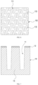
FIG. 6 is a top view of a trench formed in a method of manufacturing a semiconductor structure according to an exemplary implementation; -
FIG. 7 is a schematic sectional view of a trench formed in a method of manufacturing a semiconductor structure according to an exemplary implementation; -
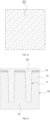
FIG. 8 is a top view of a first insulating layer formed in a method of manufacturing a semiconductor structure according to an exemplary implementation; -
FIG. 9 is a schematic sectional view of a first insulating layer formed in a method of manufacturing a semiconductor structure according to an exemplary implementation; -
FIG. 10 is a top view of an opening formed in a method of manufacturing a semiconductor structure according to an exemplary implementation; -
FIG. 11 is a schematic sectional view of an opening formed in a method of manufacturing a semiconductor structure according to an exemplary implementation; -
FIG. 12A is a schematic sectional view of polycrystalline silicon formed in a method of manufacturing a semiconductor structure according to an exemplary implementation; -
FIG. 12B is a schematic sectional view of a first metal material formed in a method of manufacturing a semiconductor structure according to an exemplary implementation; -
FIG. 13 is a schematic sectional view of a second conductive layer formed in a method of manufacturing a semiconductor structure according to an exemplary implementation; -
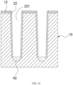
FIG. 14 is a schematic sectional view of a third metal material formed in a method of manufacturing a semiconductor structure according to an exemplary implementation; -
FIG. 15 is a schematic sectional view of a second metal material formed in a method of manufacturing a semiconductor structure according to an exemplary implementation; -
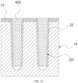
FIG. 16 is a schematic sectional view of a first conductive layer formed in a method of manufacturing a semiconductor structure according to an exemplary implementation; -
FIG. 17 is a schematic sectional view of a second insulating layer formed in a method of manufacturing a semiconductor structure according to an exemplary implementation; and -
FIG. 18 is a schematic sectional view of a WL formed in a method of manufacturing a semiconductor structure according to an exemplary implementation. - 10. substrate, 11. trench, 12. insulating layer, 13. active region, 20. isolation structure, 21. WL trench, 211. fourth insulating layer, 22. first insulating layer, 221. opening, 24. second insulating layer, 30. WL, 31. isolation layer, 32. conductive layer, 33. third insulating layer, 34. barrier layer, 40. conductive portion, 41. first conductive layer, 411. polycrystalline silicon, 412. second metal material, 42. second conductive layer, 421. first metal material, 422. third metal material, 4221. recess, 50. first contact plug, 51. second contact plug, and 52. third contact plug.
- The typical embodiments embodying the features and advantages of the present disclosure are described in detail below. It should be understood that the present disclosure may have various changes in different embodiments, which do not depart from the scope of the present disclosure. The description and accompanying drawings herein are essentially used for the purpose of explanation, rather than limiting the present disclosure.
- Different exemplary implementations of the present disclosure are described below with reference to the accompanying drawings. The accompanying drawings form a part of the present disclosure, which show by way of example different exemplary structures, systems, and steps that can implement various aspects of the present disclosure. It should be understood that other specific solutions of components, structures, exemplary apparatuses, systems, and steps may be used, and structural and functional modifications may be made without departing from the scope of the present disclosure. Moreover, although the terms such as "above", "between", and "within" may be used in this specification to describe different exemplary features and elements of the present disclosure, these terms are used herein only for convenience of description, for example, according to the directions of the examples in the accompanying drawings. Nothing in this specification should be understood as requiring a specific three-dimensional direction of the structure to fall within the scope of the present disclosure.
- An embodiment of the present disclosure provides a semiconductor structure. Referring to
FIG. 1 to FIG. 4 , the semiconductor structure includes: asubstrate 10; anisolation structure 20, formed in thesubstrate 10; aWL 30, a part of theWL 30 being located in theisolation structure 20; and aconductive portion 40, located at a bottom of theisolation structure 20, and configured to repel electrons. - The semiconductor structure provided by the embodiment of the present disclosure includes the
substrate 10, theisolation structure 20, theWL 30 and theconductive portion 40. With theconductive portion 40 at the bottom of theisolation structure 20, when theWL 30 is activated, theconductive portion 40 at the bottom of theisolation structure 20 repels surface electrons to block the leakage path, thereby preventing the electric leakage of the semiconductor structure and improving the performance of the semiconductor structure. - It is to be noted that when the
WL 30 is activated, the electrons are adsorbed by an electric field to theWL 30 and the surface of theisolation structure 20. In the related art, theisolation structure 20 is made deep enough to prevent conduction of electrons at two sides of theisolation structure 20. In the embodiment, with theconductive portion 40 at the bottom of theisolation structure 20, theconductive portion 40 repels neighboring electrons to prevent the conduction of electrons at two sides of theisolation structure 20. Therefore, the depth of theisolation structure 20 can be decreased appropriately in the embodiment. Certainly, when theisolation structure 20 is deep enough, the leakage path can be better blocked in combination with theconductive portion 40 at the bottom of theisolation structure 20. - In an embodiment, the
substrate 10 may be a p-type silicon substrate, an n-type silicon substrate, a silicon-germanium substrate, etc. - In an embodiment, the
conductive portion 40 contacts thesubstrate 10 to implement electrical connection between theconductive portion 40 and thesubstrate 10. When theWL 30 is activated, theconductive portion 40 can repel the neighboring electrons to block the leakage path. - In an embodiment, both the
conductive portion 40 and thesubstrate 10 have a negative voltage, and negative electrons are adsorbed to theWL 30 and the surface of theisolation structure 20. Theconductive portion 40 and thesubstrate 10 can repel the neighboring electrons to prevent the conduction of electrons at two sides of theisolation structure 20 and block the leakage path. - In an embodiment, as shown in
FIG. 2 , theconductive portion 40 includes: a firstconductive layer 41. With a part located in theisolation structure 20, the firstconductive layer 41 is electrically connected to thesubstrate 10, ensuring that theconductive portion 40 has the negative voltage to repel the neighboring negative electrons, preventing the conduction of electrons at two sides of theisolation structure 20 and blocking the leakage path. - In an embodiment, as shown in
FIG. 1 andFIG. 2 , the firstconductive layer 41 contacts thesubstrate 10, namely theconductive portion 40 may only include the firstconductive layer 41. The firstconductive layer 41 may be directly formed on thesubstrate 10 to implement contact between the firstconductive layer 41 and thesubstrate 10, ensuring that both theconductive portion 40 and thesubstrate 10 have the negative voltage to repel the neighboring negative electrons, preventing the conduction of electrons at two sides of theisolation structure 20 and blocking the leakage path. In the embodiment, a material of the firstconductive layer 41 includes polycrystalline silicon. By directly forming the polycrystalline silicon on thesubstrate 10, not only both theconductive portion 40 and thesubstrate 10 have the negative voltage, but the polycrystalline silicon can also be formed on thesubstrate 10 conveniently. The firstconductive layer 41 may be 20-30 nm high. In some embodiments, the material of the firstconductive layer 41 may be a metal material, such as tungsten (W), tungsten nitride (WN), titanium (Ti), titanium nitride (TiN), molybdenum (Mo), cobalt (Co), nickel (Ni), copper (Cu) or aluminum (Al). - It is to be noted that a bottom end of the first
conductive layer 41 may be flush with a bottom end of theisolation structure 20, such that the firstconductive layer 41 may be directly formed in thetrench 11 of thesubstrate 10. Or, the bottom end of the firstconductive layer 41 may be lower than the bottom end of theisolation structure 20, namely the bottom of the firstconductive layer 41 is located in thesubstrate 10 by forming a recess in a bottom wall of thetrench 11 and forming the bottom of the firstconductive layer 41 in the recess. - In an embodiment, the
conductive portion 40 further includes: a secondconductive layer 42. The secondconductive layer 42 contacts thesubstrate 10. The firstconductive layer 41 is located on an upper surface of the secondconductive layer 42 to implement contact between the firstconductive layer 41 and the secondconductive layer 42. As shown inFIG. 3 andFIG. 4 , theconductive portion 40 includes a firstconductive layer 41 and a secondconductive layer 42. The secondconductive layer 42 is located in thesubstrate 10, and electrically connected to thesubstrate 10, and the firstconductive layer 41 is electrically connected to thesubstrate 10 through the secondconductive layer 42, such that both theconductive portion 40 and thesubstrate 10 have the negative voltage and can repel the neighboring negative electrons, thereby preventing the conduction of electrons at two sides of theisolation structure 20 and blocking the leakage path. - In an embodiment, a bottom of the first
conductive layer 41 is located in the secondconductive layer 42 to implement more stable conduction between the firstconductive layer 41 and the secondconductive layer 42. - In an embodiment, a bottom end of the first
conductive layer 41 abuts against a top end of the secondconductive layer 42. - In an embodiment, a material of the first
conductive layer 41 includes a metal material, while a material of the secondconductive layer 42 includes metal silicide. The firstconductive layer 41 is electrically connected to thesubstrate 10, and the secondconductive layer 42 may be formed in thesubstrate 10. The firstconductive layer 41 may be 20-30 nm high, while the secondconductive layer 42 may be 10-20 nm high. - In some embodiments, the metal material may include, but is not limited to: tungsten (W), tungsten nitride (WN), titanium (Ti), titanium nitride (TiN), molybdenum (Mo), cobalt (Co), nickel (Ni), copper (Cu) or aluminum (Al). The metal silicide may include, but is not limited to: at least one of nickel silicide, platinum silicide and cobalt silicide.
- In an embodiment, the
isolation structure 20 is a shallow trench isolation (STI) structure. By forming theconductive portion 40 in the STI structure, the isolation capability of the STI structure can be improved to prevent the electric leakage, and the depth of the STI structure can be decreased appropriately. - In an embodiment, as shown in
FIG. 1 , the semiconductor structure further includes: afirst contact plug 50, and asecond contact plug 51. Thefirst contact plug 50 and thesecond contact plug 51 are located at two sides of theWL 30. Both thefirst contact plug 50 and thesecond contact plug 51 are a capacitance contact plug. Thefirst contact plug 50 and thesecond contact plug 51 are configured to connect two capacitor structures. When theWL 30 is activated, thefirst contact plug 50 and thesecond contact plug 51 are connected to the electrons at two sides of theisolation structure 20. While the electrons at two sides of theisolation structure 20 are connected, thefirst contact plug 50 and thesecond contact plug 51 are also connected to cause the electric leakage between the two capacitor structures. In the embodiment, since theconductive portion 40 is formed at the bottom of theisolation structure 20 and theconductive portion 40 repels the neighboring electrons, the conduction of electrons at two sides of theisolation structure 20 can be blocked to prevent the electric leakage between the two capacitor structures. - It is to be noted that the semiconductor structure may further include a
third contact plug 52, as shown inFIG. 1 andFIG. 3 . There may be a plurality of the first contact plugs 50, a plurality of the second contact plugs 51 and a plurality of the third contact plugs 52, which is not limited herein and may be determined according to actual needs. - In an embodiment, the
conductive portion 40 is located below theWL 30, and insulated from theWL 30. When theWL 30 is activated, theconductive portion 40 repels the neighboring electrons to prevent the conduction of electrons at two sides of theisolation structure 20. - In an embodiment, a height of the
conductive portion 40 is less than a distance between theconductive portion 40 and theWL 30. That is, while theconductive portion 40 blocks the leakage path, theconductive portion 40 can be made as small as possible. - In an embodiment, as shown in
FIG. 1 andFIG. 3 , anisolation layer 31 is formed in theisolation structure 20. Theisolation layer 31 is located on theWL 30. Theisolation layer 31 can protect theWL 30. In an embodiment, theisolation layer 31 may include nitride or silicon oxide. - In an embodiment, as shown in
FIG. 1 andFIG. 3 , an insulatinglayer 12 is formed on an upper surface of thesubstrate 10 to cover the upper surface of thesubstrate 10. Theisolation structure 20 in thesubstrate 10 is integrally formed, and thus an insulating material formed into theisolation structure 20 covers the upper surface of thesubstrate 10. The insulatinglayer 12 covers the insulating material. The insulatinglayer 12 may include nitride or silicon oxide. - In an embodiment, the
WL 30 is a buried WL. A material of theWL 30 includes one or any combination of tungsten, titanium, nickel, aluminum, platinum, titanium nitride and other conductive materials. In some embodiments, anisolation layer 31 is further formed in aWL trench 21. Theisolation layer 31 is located on theWL 30. Theisolation layer 31 can protect theWL 30. Upon formation of theisolation layer 31, theisolation layer 31 may be planarized with dry etching or chemical mechanical polishing (CMP). - In an embodiment, an
isolation structure 20 is formed in thesubstrate 10. Theisolation structure 20 isolates a plurality ofactive regions 13. TheWL 30 is located in theisolation structure 20 and in theactive region 13. In some embodiments, theconductive portion 40 may be provided below theWL 30 in theisolation structure 20. In some embodiments, theconductive portion 40 may not be provided below one or more WLs 30 among a plurality ofWLs 30 in theisolation structure 20. When two capacitance contact plugs (such as thefirst contact plug 50 and the second contact plug 51) are formed at two sides of theisolation structure 20, theconductive portion 40 is provided below the correspondingWL 30 in theisolation structure 20 to prevent the electric leakage between the two capacitor structures. - In an embodiment, the
WL 30 may include a plurality of protrusive structures that may be located in theisolation structure 20 and theactive region 13. The protrusive structures may have a same height, and may also have different heights. - An embodiment of the present disclosure further provides a method of manufacturing a semiconductor structure. As shown in
FIG. 5 , the method of manufacturing a semiconductor structure includes the following steps: - S101: Provide a
substrate 10. - S103: Form a
trench 11 in thesubstrate 10. - S105: Form an
isolation structure 20 in thetrench 11, and form, at a bottom of theisolation structure 20, aconductive portion 40 for repelling electrons. - S107: Form a
WL trench 21 in theisolation structure 20. - S109: Form a
WL 30 in theWL trench 21. - According to the method of manufacturing a semiconductor structure provided by the embodiment of the present disclosure, the
trench 11 is formed in thesubstrate 10, theisolation structure 20 is formed in thetrench 11, theconductive portion 40 is formed at the bottom of theisolation structure 20, and theWL 30 is formed in theWL trench 21 of theisolation structure 20. Theconductive portion 40 at the bottom of theisolation structure 20 can repel surface electrons to block the leakage path, thereby preventing the electric leakage of the semiconductor structure and improving the performance of the semiconductor structure. - In an embodiment, as shown in
FIG. 6 and FIG. 7 , thetrench 11 is formed in thesubstrate 10, and a plurality ofactive regions 13 are isolated in thetrench 11. Thetrench 11 may be formed by STI. - In an embodiment, an insulating
layer 12 is formed on an upper surface of thesubstrate 10. During formation of thetrench 11, a mask structure may cover the insulatinglayer 12, and a pattern corresponding to thetrench 11 may be formed on the insulatinglayer 12, thereby etching a through hole in the insulatinglayer 12 and forming a recess in thesubstrate 10 to form thetrench 11, as shown inFIG. 6 and FIG. 7 . - In an embodiment, before a part of the
conductive portion 40 is formed in theisolation structure 20, the conductive portion is formed in thetrench 11 and contacts thesubstrate 10, which can ensure that both theconductive portion 40 and thesubstrate 10 has a negative voltage, and theconductive portion 40 and thesubstrate 10 repel neighboring electrons, thereby preventing the electron conduction at two sides of theisolation structure 20 and blocking the leakage path. - It is to be noted that the
conductive portion 40 cannot be formed at the bottom of theisolation structure 20, unless theconductive portion 40 is formed before theisolation structure 20 is formed completely. - In an embodiment, a first
conductive layer 41 is formed in thetrench 11, the firstconductive layer 41 serving as theconductive portion 40. Specifically, upon formation of thetrench 11, the firstconductive layer 41 may be formed at a bottom of thetrench 11. The firstconductive layer 41 may fill up the bottom of thetrench 11. The firstconductive layer 41 is etched to expose a bottom sidewall of thetrench 11. Theisolation structure 20 is filled in thetrench 11 to cover the firstconductive layer 41. Optionally, a part of theisolation structure 20 is filled in thetrench 11, an opening is formed in the isolation structure to expose thesubstrate 10, and the firstconductive layer 41 is formed in the opening. Thereafter, a remaining part of theisolation structure 20 is filled in thetrench 11 to cover the firstconductive layer 41. - In an embodiment, a second
conductive layer 42 is formed in thesubstrate 10. A firstconductive layer 41 is formed on the secondconductive layer 42. A part of the firstconductive layer 41 is formed in thetrench 11. The firstconductive layer 41 and the secondconductive layer 42 serve as theconductive portion 40. Specifically, a recess may be formed in thesubstrate 10 through thetrench 11. A secondconductive layer 42 is formed in the recess. A firstconductive layer 41 is formed at the bottom of thetrench 11. The firstconductive layer 41 may fill up the bottom of thetrench 11. The firstconductive layer 41 is etched to expose a bottom sidewall of thetrench 11. Theisolation structure 20 is filled in thetrench 11 to cover the firstconductive layer 41. Optionally, a recess may be formed in thesubstrate 10 through thetrench 11. A secondconductive layer 42 is formed in the recess. A part of theisolation structure 20 is filled in thetrench 11, an opening is formed in the isolation structure to expose the secondconductive layer 42, and the firstconductive layer 41 is formed in the opening. Thereafter, a remaining part of theisolation structure 20 is filled in thetrench 11 to cover the firstconductive layer 41. Optionally, a metal material is deposited in thesubstrate 10 through thetrench 11 and annealed to form the secondconductive layer 42. The firstconductive layer 41 may be formed according to the above two manners. - It is to be noted that by depositing the metal material in the
substrate 10 provided with thetrench 11, the metal material reacts with silicon in thesubstrate 10 to form the secondconductive layer 42. The metal material may be deposited by physical vapor deposition (PVD), chemical vapor deposition (CVD) or atomic layer deposition (ALD). The metal material may include one or more of nickel, platinum, cobalt and so on. In some embodiments, upon deposition of the metal material in thesubstrate 10, annealing is performed to form the secondconductive layer 42. The annealing may be hightemperature furnace tube propulsion, and may also be rapid thermal annealing (RTA) in the related art. - In an embodiment, the step of forming a
conductive portion 40 includes: Form a firstconductive layer 41 in thetrench 11, the firstconductive layer 41 serving as theconductive portion 40. A first insulatinglayer 22 is formed between the firstconductive layer 41 and a sidewall of thetrench 11 to ensure insulation between the firstconductive layer 41 and the sidewall of thetrench 11. Therefore, while theconductive portion 40 can repel surface electrons, the firstconductive layer 41 cannot be overlarge. - In some embodiments, the first insulating
layer 22 is formed in thetrench 11, the first insulatinglayer 22 filling up thetrench 11 and covering the insulatinglayer 12, as shown inFIG. 8 and FIG. 9 . The first insulatinglayer 22 may be nitride or silicon oxide. The first insulatinglayer 22 may be formed with the PVD, the CVD or the ALD. - An
opening 221 is formed in the first insulatinglayer 22, and theopening 221 exposes thesubstrate 10, namely the first insulatinglayer 22 covers a sidewall of theopening 221, as shown inFIG. 10 and FIG. 11 . In some embodiments, there remains a part of the first insulatinglayer 22 on the insulatinglayer 12, as shown inFIG. 10 . In some embodiments, the first insulatinglayer 22 on the insulatinglayer 12 can be removed completely, as shown inFIG. 11 . Theopening 221 may be etched. Theopening 221 serves as a part of thetrench 11. - In an embodiment,
polycrystalline silicon 411 is deposited in thetrench 11 to form the firstconductive layer 41, namely thepolycrystalline silicon 411 serves as theconductive portion 40 to repel the neighboring electrons. - In some embodiments,
polycrystalline silicon 411 is deposited in theopening 221, thepolycrystalline silicon 411 filling up theopening 221 and covering the insulatinglayer 12, as shown inFIG. 12A . Thepolycrystalline silicon 411 on the insulatinglayer 12 and a part of thepolycrystalline silicon 411 in theopening 221 are removed by etching. The remainingpolycrystalline silicon 411 is 20-30 nm high to serve as theconductive portion 40. - In an embodiment, the step of forming a
conductive portion 40 includes: Form a secondconductive layer 42 on thesubstrate 10 through thetrench 11; and form a firstconductive layer 41 on an upper surface of the secondconductive layer 42, the firstconductive layer 41 and the secondconductive layer 42 serving as theconductive portion 40. The firstconductive layer 41 is formed in thetrench 11, and a first insulatinglayer 22 is formed between the firstconductive layer 41 and a sidewall of thetrench 11. The firstconductive layer 41 is electrically connected to thesubstrate 10 through the secondconductive layer 42, such that both theconductive portion 40 and thesubstrate 10 have the negative voltage, and can repel the neighboring electrons, thereby preventing the conduction of electrons at two sides of theisolation structure 20 and blocking the leakage path. - In an embodiment, a
first metal material 421 is deposited in thesubstrate 10 and thermally treated to form metal silicide, the metal silicide serving as the secondconductive layer 42. Asecond metal material 412 is formed on the metal silicide, thesecond metal material 412 serving as the firstconductive layer 41. The firstconductive layer 41 and the secondconductive layer 42 are separately formed by thefirst metal material 421 and thesecond metal material 412, and are connected to each other to repel the neighboring electrons, thereby preventing the conduction of electrons at two sides of theisolation structure 20 and blocking the leakage path. - In some embodiments, upon formation of the
opening 221 in the first insulatinglayer 22, afirst metal material 421 is deposited in theopening 221. Thefirst metal material 421 fills up theopening 221, and covers the insulatinglayer 12. After thermally treated, thefirst metal material 421 reacts with thesubstrate 10 to form the metal silicide. The metal silicide serves as the secondconductive layer 42, as shown inFIG. 12B . The thermal treatment may be performed at 340-450°C. - The
first metal material 421 contacting thesubstrate 10 and a part of the metal silicide are removed with wet etching to expose the secondconductive layer 42, as shown inFIG. 13 . The remaining metal silicide may be 10-20 nm high, namely the secondconductive layer 42 may be 10-20 nm high. - In an embodiment, before formation of the first
conductive layer 41, athird metal material 422 is formed on a wall of the first insulatinglayer 22. The firstconductive layer 41 is formed in thethird metal material 422. Thethird metal material 422 protects the firstconductive layer 41. - The
third metal material 422 is deposited in theopening 221. Thethird metal material 422 fills up theopening 221, covers the insulatinglayer 12, and contacts the secondconductive layer 42, as shown inFIG. 14 . Thesecond metal material 412 may be tungsten. Thethird metal material 422 may be metal nitride, such as thethird metal material 422 may be titanium nitride. - A
recess 4221 is formed in thethird metal material 422, and thesecond metal material 412 is deposited in therecess 4221. Thesecond metal material 412 fills up therecess 4221, and covers an upper surface of thethird metal material 422, as shown inFIG. 15 . - The
second metal material 412 and thethird metal material 422 are etched. There remains a part of thesecond metal material 412 and a part of thethird metal material 422 in theopening 221. The remainingsecond metal material 412 serves as the firstconductive layer 41, and the firstconductive layer 41 is located in the remainingthird meal material 422, as shown inFIG. 16 . The remainingsecond metal material 412 may be 20-30 nm high. - In some embodiments, the
conductive portion 40 may include the metal silicide formed by thefirst metal material 421 and thesubstrate 10, thesecond metal material 412 and thethird metal material 422. - In an embodiment, the
WL trench 21 is formed in theisolation structure 20 and in theactive region 13. TheWL 30 is formed in theWL trench 21 of each of theisolation structure 20 and theactive region 13. - In an embodiment, upon formation of the
conductive portion 40, there remains a part of theopening 221 on theconductive portion 40, as shown inFIG. 16 . A second insulatinglayer 24 is formed in theopening 221. The second insulatinglayer 24 fills the exposedopening 221, and covers the insulatinglayer 12, as shown inFIG. 17 . - A plurality of the
WL trenches 21 are formed in the second insulatinglayer 24 and theactive region 13. TheWL 30 is formed in theWL trench 21. - In an embodiment, a part of the second insulating
layer 24 is removed to expose theopening 221 in the second insulatinglayer 24, namely the exposedopening 221 serves as theWL trench 21 in theisolation structure 20. TheWL trench 21 is also formed in theactive region 13. The first insulatinglayer 22 and the second insulatinglayer 24 may serve as theisolation structure 20. - The
WL 30 may include abarrier layer 34, aconductive layer 32 and a third insulatinglayer 33. Thebarrier layer 34 covers a wall of theWL trench 21. Theconductive layer 32 is located in thebarrier layer 34. The third insulatinglayer 33 covers thebarrier layer 34 and theconductive layer 32, as shown inFIG. 18 . - After the
barrier layer 34 is deposited in theWL trench 21, thebarrier layer 34 fills up theWL trench 21, and is etched to make a remaining part of thebarrier layer 34 cover the wall of theWL trench 21. Theconductive layer 32 is filled in thebarrier layer 34. Theconductive layer 32 is etched, such that an upper surface of theconductive layer 32 is flush with an upper surface of thebarrier layer 34. The third insulatinglayer 33 is formed at last. - In an embodiment, the
barrier layer 34 may include Ta, Ti, Ru, TaN, TiN, RuTa, RuTaN, W or Ir. Thebarrier layer 34 may be formed by any material capable of preventing diffusion of the conductive material layer. In an embodiment, theconductive layer 32 may be formed by a metal material such as Cu, Al, W or alloy. In an embodiment, the third insulatinglayer 33 may be formed by a material including silicon oxide, silicon nitride or a combination thereof. For example, the third insulatinglayer 33 may be formed by SIN, SION or SIO2. - In an embodiment, upon formation of the
WL trench 21, a fourth insulatinglayer 211 is formed on a sidewall of theWL trench 21. TheWL 30 is formed in the fourth insulatinglayer 211. The fourth insulatinglayer 211 may be formed by a material including silicon oxide, silicon nitride or a combination thereof. For example, the fourth insulatinglayer 211 may be formed by SIN, SION or SIO2. - It is to be noted that when the first
conductive layer 41 serves as theconductive portion 40, after thepolycrystalline silicon 411 shown inFIG. 12A is formed, the second insulatinglayer 24 is formed on thepolycrystalline silicon 411, theWL trench 21 is formed in each of theisolation structure 20 and theactive region 13, and theWL 30 is formed in theWL trench 21 in each of theisolation structure 20 and theactive region 13. The specific structure and process may refer to those when the firstconductive layer 41 and the secondconductive layer 42 serves as theconductive portion 40. - In an embodiment, the method of manufacturing a semiconductor structure further includes: Form a
first contact plug 50 and asecond contact plug 51 at two sides of theWL 30. Both thefirst contact plug 50 and thesecond contact plug 51 are a capacitance contact plug. Thefirst contact plug 50 and thesecond contact plug 51 are configured to connect two capacitor structures. When theWL 30 is activated, thefirst contact plug 50 and thesecond contact plug 51 are connected to the electrons at two sides of theisolation structure 20. While the electrons at two sides of theisolation structure 20 are connected, thefirst contact plug 50 and thesecond contact plug 51 are also connected to cause the electric leakage between the two capacitor structures. In the embodiment, since theconductive portion 40 is formed at the bottom of theisolation structure 20 and theconductive portion 40 repels the neighboring electrons, the conduction of electrons at two sides of theisolation structure 20 can be blocked to prevent the electric leakage between the two capacitor structures. - The semiconductor structure formed with the method is provided with the
conductive portion 40 at the bottom of theisolation structure 20. Theconductive portion 40 can repel the electrons, thereby reducing the current leakage of the semiconductor structure and improving the performance of the semiconductor structure. The semiconductor structure is applied to the DRAM device with the small size and the high performance. - It should be noted that the semiconductor structure in the embodiment is obtained through the method of manufacturing a semiconductor structure. For other materials and structures of the semiconductor structure in the embodiment, reference may be made to the method of manufacturing a semiconductor structure.
- Those skilled in the art may easily figure out other implementations of the present disclosure after considering the specification and practicing the invention disclosed herein. The present disclosure is intended to cover any variations, purposes, or applicable changes of the present disclosure. Such variations, purposes or applicable changes follow the general principle of the present disclosure and include common knowledge or conventional technical means in the technical field which is not disclosed in the present disclosure. The specification and implementations are merely considered as illustrative, and the real scope and spirit of the present disclosure are directed by the appended claims.
- It should be noted that, the present disclosure is not limited to the precise structures described above and shown in the drawings, and can be modified and changed in many ways without departing from the scope of the present disclosure. The scope of the present disclosure is defined by the appended claims.
Claims (20)
- A semiconductor structure, comprising:a substrate;an isolation structure, formed in the substrate;a word line, a part of the word line being located in the isolation structure; anda conductive portion, located at a bottom of the isolation structure.
- The semiconductor structure according to claim 1, wherein the conductive portion contacts the substrate.
- The semiconductor structure according to claim 2, wherein a voltage of the conductive portion and a voltage of the substrate are a negative voltage.
- The semiconductor structure according to claim 2, wherein the conductive portion comprises:
a first conductive layer, a part of the first conductive layer being located in the isolation structure. - The semiconductor structure according to claim 4, wherein the first conductive layer contacts the substrate; and
a material of the first conductive layer comprises polycrystalline silicon. - The semiconductor structure according to claim 4, wherein the conductive portion further comprises:
a second conductive layer, contacting the substrate, the first conductive layer being located on an upper surface of the second conductive layer. - The semiconductor structure according to claim 6, wherein a material of the first conductive layer comprises a metal material, while a material of the second conductive layer comprises metal silicide.
- The semiconductor structure according to claim 6, wherein a bottom of the first conductive layer is located in the second conductive layer.
- The semiconductor structure according to claim 1, wherein the word line is a buried word line.
- The semiconductor structure according to claim 1, wherein the isolation structure is a shallow trench isolation structure.
- The semiconductor structure according to claim 1, further comprising:a first contact plug; anda second contact plug, wherein the first contact plug and the second contact plug are located at two sides of the word line; andboth the first contact plug and the second contact plug are a capacitance contact plug.
- The semiconductor structure according to claim 1, wherein the conductive portion is located below the word line, and insulated from the word line.
- The semiconductor structure according to claim 12, wherein a height of the conductive portion is less than a distance between the conductive portion and the word line.
- A method of manufacturing a semiconductor structure, comprising:providing a substrate;forming a trench in the substrate;forming an isolation structure in the trench, and forming a conductive portion at a bottom of the isolation structure;forming a word line trench in the isolation structure; andforming a word line in the word line trench.
- The method of manufacturing the semiconductor structure according to claim 14, wherein the forming a conductive portion comprises:forming a first conductive layer in the trench, the first conductive layer serving as the conductive portion, whereina first insulating layer is formed between the first conductive layer and a sidewall of the trench.
- The method of manufacturing the semiconductor structure according to claim 15, wherein polycrystalline silicon is deposited in the trench to form the first conductive layer.
- The method of manufacturing the semiconductor structure according to claim 14, wherein the forming a conductive portion comprises:forming a second conductive layer on the substrate through the trench; andforming a first conductive layer on an upper surface of the second conductive layer, the first conductive layer and the second conductive layer serving as the conductive portion,wherein the first conductive layer is formed in the trench, and a first insulating layer is formed between the first conductive layer and a sidewall of the trench.
- The method of manufacturing the semiconductor structure according to claim 17, wherein a first metal material is deposited in the substrate and thermally treated to form metal silicide, the metal silicide serving as the second conductive layer; and
a second metal material is formed on the metal silicide, the second metal material serving as the first conductive layer. - The method of manufacturing the semiconductor structure according to claim 17 or 18, before the forming a first conductive layer, further comprising: forming a third metal material on a wall of the first insulating layer, wherein
the first conductive layer is formed in the third metal material. - The method of manufacturing the semiconductor structure according to any one of claims 15 to 18, wherein the substrate is provided with a plurality of active regions, and the isolation structure is provided between the active regions;the word line trench is also formed in each of the active regions, and a part of the word line is formed in the word line trench in each of the active regions; andbefore the word line is formed, a second insulating layer is formed on the first conductive layer to insulate and isolate the word line and the first conductive layer.
Applications Claiming Priority (2)
| Application Number | Priority Date | Filing Date | Title |
|---|---|---|---|
| CN202111242748.9A CN116033738B (en) | 2021-10-25 | 2021-10-25 | Semiconductor structure and method for manufacturing semiconductor structure |
| PCT/CN2022/070379 WO2023070944A1 (en) | 2021-10-25 | 2022-01-05 | Semiconductor structure and method for manufacturing semiconductor structure |
Publications (2)
| Publication Number | Publication Date |
|---|---|
| EP4412422A1 true EP4412422A1 (en) | 2024-08-07 |
| EP4412422A4 EP4412422A4 (en) | 2025-02-12 |
Family
ID=85156744
Family Applications (1)
| Application Number | Title | Priority Date | Filing Date |
|---|---|---|---|
| EP22884864.4A Pending EP4412422A4 (en) | 2021-10-25 | 2022-01-05 | Semiconductor structure and method for manufacturing semiconductor structure |
Country Status (2)
| Country | Link |
|---|---|
| US (1) | US11574913B1 (en) |
| EP (1) | EP4412422A4 (en) |
Family Cites Families (8)
| Publication number | Priority date | Publication date | Assignee | Title |
|---|---|---|---|---|
| KR100441569B1 (en) | 2000-03-17 | 2004-07-23 | 프로모스 테크놀로지스 인코퍼레이티드 | Structure of dram with vertical transistor and method of fabricating the same |
| KR100966265B1 (en) * | 2008-02-15 | 2010-06-28 | 재단법인서울대학교산학협력재단 | NAND flash memory array with blocking gate line and its operation and manufacturing method |
| JP2012222285A (en) * | 2011-04-13 | 2012-11-12 | Elpida Memory Inc | Semiconductor device and method of manufacturing the same |
| CN106783743B (en) | 2015-11-23 | 2019-07-26 | 华邦电子股份有限公司 | Memory device and its manufacturing method |
| CN108565263B (en) * | 2018-05-30 | 2023-09-26 | 长鑫存储技术有限公司 | Semiconductor device and manufacturing method |
| CN110957318A (en) * | 2018-09-26 | 2020-04-03 | 长鑫存储技术有限公司 | Semiconductor structure and manufacturing method thereof |
| CN110970346A (en) | 2018-09-29 | 2020-04-07 | 长鑫存储技术有限公司 | Semiconductor structure and preparation method |
| CN208903993U (en) | 2018-11-19 | 2019-05-24 | 长鑫存储技术有限公司 | Fleet plough groove isolation structure |
-
2022
- 2022-01-05 EP EP22884864.4A patent/EP4412422A4/en active Pending
- 2022-05-25 US US17/664,906 patent/US11574913B1/en active Active
Also Published As
| Publication number | Publication date |
|---|---|
| US11574913B1 (en) | 2023-02-07 |
| EP4412422A4 (en) | 2025-02-12 |
Similar Documents
| Publication | Publication Date | Title |
|---|---|---|
| US10497704B2 (en) | Buried word line structure and method of making the same | |
| TWI780753B (en) | Semiconductor devices | |
| US12356611B2 (en) | Semiconductor device and method for fabricating the same | |
| US7525142B2 (en) | Semiconductor device including a conductive layer buried in an opening and method of manufacturing the same | |
| CN102222668A (en) | Semiconductor device and method for forming the same | |
| CN111403388A (en) | Semiconductor device and method of manufacturing the same | |
| CN112786527B (en) | Semiconductor structure and manufacturing method thereof | |
| TWI892342B (en) | Semiconductor device | |
| US20200111794A1 (en) | Method for fabricating semiconductor device | |
| US12426339B2 (en) | Buried gate semiconductor device having a dielectric layer between two electrodes | |
| CN109962074A (en) | Semiconductor memory structure and method of making the same | |
| KR101604040B1 (en) | Method of manufacturing semiconductor memory devices | |
| US6239010B1 (en) | Method for manually manufacturing capacitor | |
| US6265262B1 (en) | Semiconductor device and method of fabricating the same | |
| US11688783B1 (en) | Semiconductor device and method for manufacturing the same | |
| JP4639524B2 (en) | Manufacturing method of semiconductor device | |
| US11574913B1 (en) | Semiconductor structure and manufacturing method thereof | |
| US11895830B2 (en) | Method for manufacturing semiconductor device | |
| US12113100B2 (en) | Semiconductor structure and method for manufacturing semiconductor structure | |
| CN116033738B (en) | Semiconductor structure and method for manufacturing semiconductor structure | |
| CN116247031B (en) | Semiconductor element and method for manufacturing the same | |
| TWI901315B (en) | Conductive structure, semiconductor device and manufacturing method thereof | |
| TWI890255B (en) | Semiconductor structure and method for forming the same | |
| JP4729863B2 (en) | Semiconductor memory device and manufacturing method thereof | |
| KR20100111378A (en) | Contact plug, semiconductor device having the same and method of manufacturing the same |
Legal Events
| Date | Code | Title | Description |
|---|---|---|---|
| STAA | Information on the status of an ep patent application or granted ep patent |
Free format text: STATUS: THE INTERNATIONAL PUBLICATION HAS BEEN MADE |
|
| PUAI | Public reference made under article 153(3) epc to a published international application that has entered the european phase |
Free format text: ORIGINAL CODE: 0009012 |
|
| STAA | Information on the status of an ep patent application or granted ep patent |
Free format text: STATUS: REQUEST FOR EXAMINATION WAS MADE |
|
| 17P | Request for examination filed |
Effective date: 20240502 |
|
| AK | Designated contracting states |
Kind code of ref document: A1 Designated state(s): AL AT BE BG CH CY CZ DE DK EE ES FI FR GB GR HR HU IE IS IT LI LT LU LV MC MK MT NL NO PL PT RO RS SE SI SK SM TR |
|
| DAV | Request for validation of the european patent (deleted) | ||
| DAX | Request for extension of the european patent (deleted) | ||
| A4 | Supplementary search report drawn up and despatched |
Effective date: 20250115 |
|
| RIC1 | Information provided on ipc code assigned before grant |
Ipc: H01L 21/762 20060101ALI20250109BHEP Ipc: H10B 12/00 20230101AFI20250109BHEP |
|
| RIC1 | Information provided on ipc code assigned before grant |
Ipc: H10B 12/00 20230101AFI20251001BHEP Ipc: H01L 21/762 20060101ALI20251001BHEP |
|
| GRAP | Despatch of communication of intention to grant a patent |
Free format text: ORIGINAL CODE: EPIDOSNIGR1 |
|
| STAA | Information on the status of an ep patent application or granted ep patent |
Free format text: STATUS: GRANT OF PATENT IS INTENDED |
|
| GRAJ | Information related to disapproval of communication of intention to grant by the applicant or resumption of examination proceedings by the epo deleted |
Free format text: ORIGINAL CODE: EPIDOSDIGR1 |
|
| STAA | Information on the status of an ep patent application or granted ep patent |
Free format text: STATUS: REQUEST FOR EXAMINATION WAS MADE |
|
| INTG | Intention to grant announced |
Effective date: 20251118 |
|
| INTC | Intention to grant announced (deleted) | ||
| GRAP | Despatch of communication of intention to grant a patent |
Free format text: ORIGINAL CODE: EPIDOSNIGR1 |
|
| STAA | Information on the status of an ep patent application or granted ep patent |
Free format text: STATUS: GRANT OF PATENT IS INTENDED |
|
| INTG | Intention to grant announced |
Effective date: 20260209 |
|
| RIC1 | Information provided on ipc code assigned before grant |
Ipc: H10B 12/00 20230101AFI20260205BHEP Ipc: H10W 10/10 20260101ALI20260205BHEP |
|
| P01 | Opt-out of the competence of the unified patent court (upc) registered |
Free format text: CASE NUMBER: UPC_APP_0009784_4412422/2026 Effective date: 20260313 |