EP4412410A1 - Wiring substrate - Google Patents
Wiring substrate Download PDFInfo
- Publication number
- EP4412410A1 EP4412410A1 EP22876004.7A EP22876004A EP4412410A1 EP 4412410 A1 EP4412410 A1 EP 4412410A1 EP 22876004 A EP22876004 A EP 22876004A EP 4412410 A1 EP4412410 A1 EP 4412410A1
- Authority
- EP
- European Patent Office
- Prior art keywords
- via conductor
- continuous phase
- insulation layer
- wiring board
- ceramic
- Prior art date
- Legal status (The legal status is an assumption and is not a legal conclusion. Google has not performed a legal analysis and makes no representation as to the accuracy of the status listed.)
- Pending
Links
Images


Classifications
-
- H—ELECTRICITY
- H05—ELECTRIC TECHNIQUES NOT OTHERWISE PROVIDED FOR
- H05K—PRINTED CIRCUITS; CASINGS OR CONSTRUCTIONAL DETAILS OF ELECTRIC APPARATUS; MANUFACTURE OF ASSEMBLAGES OF ELECTRICAL COMPONENTS
- H05K1/00—Printed circuits
- H05K1/02—Details
- H05K1/03—Use of materials for the substrate
- H05K1/0306—Inorganic insulating substrates, e.g. ceramic, glass
-
- C—CHEMISTRY; METALLURGY
- C04—CEMENTS; CONCRETE; ARTIFICIAL STONE; CERAMICS; REFRACTORIES
- C04B—LIME, MAGNESIA; SLAG; CEMENTS; COMPOSITIONS THEREOF, e.g. MORTARS, CONCRETE OR LIKE BUILDING MATERIALS; ARTIFICIAL STONE; CERAMICS; REFRACTORIES; TREATMENT OF NATURAL STONE
- C04B35/00—Shaped ceramic products characterised by their composition; Ceramics compositions; Processing powders of inorganic compounds preparatory to the manufacturing of ceramic products
-
- C—CHEMISTRY; METALLURGY
- C04—CEMENTS; CONCRETE; ARTIFICIAL STONE; CERAMICS; REFRACTORIES
- C04B—LIME, MAGNESIA; SLAG; CEMENTS; COMPOSITIONS THEREOF, e.g. MORTARS, CONCRETE OR LIKE BUILDING MATERIALS; ARTIFICIAL STONE; CERAMICS; REFRACTORIES; TREATMENT OF NATURAL STONE
- C04B35/00—Shaped ceramic products characterised by their composition; Ceramics compositions; Processing powders of inorganic compounds preparatory to the manufacturing of ceramic products
- C04B35/01—Shaped ceramic products characterised by their composition; Ceramics compositions; Processing powders of inorganic compounds preparatory to the manufacturing of ceramic products based on oxide ceramics
- C04B35/16—Shaped ceramic products characterised by their composition; Ceramics compositions; Processing powders of inorganic compounds preparatory to the manufacturing of ceramic products based on oxide ceramics based on silicates other than clay
- C04B35/18—Shaped ceramic products characterised by their composition; Ceramics compositions; Processing powders of inorganic compounds preparatory to the manufacturing of ceramic products based on oxide ceramics based on silicates other than clay rich in aluminium oxide
- C04B35/185—Mullite 3Al2O3-2SiO2
-
- H—ELECTRICITY
- H05—ELECTRIC TECHNIQUES NOT OTHERWISE PROVIDED FOR
- H05K—PRINTED CIRCUITS; CASINGS OR CONSTRUCTIONAL DETAILS OF ELECTRIC APPARATUS; MANUFACTURE OF ASSEMBLAGES OF ELECTRICAL COMPONENTS
- H05K1/00—Printed circuits
- H05K1/02—Details
- H05K1/0271—Arrangements for reducing stress or warp in rigid printed circuit boards, e.g. caused by loads, vibrations or differences in thermal expansion
-
- H—ELECTRICITY
- H05—ELECTRIC TECHNIQUES NOT OTHERWISE PROVIDED FOR
- H05K—PRINTED CIRCUITS; CASINGS OR CONSTRUCTIONAL DETAILS OF ELECTRIC APPARATUS; MANUFACTURE OF ASSEMBLAGES OF ELECTRICAL COMPONENTS
- H05K1/00—Printed circuits
- H05K1/02—Details
- H05K1/03—Use of materials for the substrate
- H05K1/0313—Organic insulating material
- H05K1/0353—Organic insulating material consisting of two or more materials, e.g. two or more polymers, polymer + filler, + reinforcement
- H05K1/0366—Organic insulating material consisting of two or more materials, e.g. two or more polymers, polymer + filler, + reinforcement reinforced, e.g. by fibres, fabrics
-
- H—ELECTRICITY
- H05—ELECTRIC TECHNIQUES NOT OTHERWISE PROVIDED FOR
- H05K—PRINTED CIRCUITS; CASINGS OR CONSTRUCTIONAL DETAILS OF ELECTRIC APPARATUS; MANUFACTURE OF ASSEMBLAGES OF ELECTRICAL COMPONENTS
- H05K1/00—Printed circuits
- H05K1/02—Details
- H05K1/03—Use of materials for the substrate
- H05K1/05—Insulated conductive substrates, e.g. insulated metal substrate
- H05K1/056—Insulated conductive substrates, e.g. insulated metal substrate the metal substrate being covered by an organic insulating layer
-
- H—ELECTRICITY
- H05—ELECTRIC TECHNIQUES NOT OTHERWISE PROVIDED FOR
- H05K—PRINTED CIRCUITS; CASINGS OR CONSTRUCTIONAL DETAILS OF ELECTRIC APPARATUS; MANUFACTURE OF ASSEMBLAGES OF ELECTRICAL COMPONENTS
- H05K1/00—Printed circuits
- H05K1/02—Details
- H05K1/09—Use of materials for the conductive, e.g. metallic pattern
-
- H—ELECTRICITY
- H05—ELECTRIC TECHNIQUES NOT OTHERWISE PROVIDED FOR
- H05K—PRINTED CIRCUITS; CASINGS OR CONSTRUCTIONAL DETAILS OF ELECTRIC APPARATUS; MANUFACTURE OF ASSEMBLAGES OF ELECTRICAL COMPONENTS
- H05K1/00—Printed circuits
- H05K1/02—Details
- H05K1/11—Printed elements for providing electric connections to or between printed circuits
- H05K1/111—Pads for surface mounting, e.g. lay-out
- H05K1/112—Pads for surface mounting, e.g. lay-out directly combined with via connections
- H05K1/113—Via provided in pad; Pad over filled via
-
- H—ELECTRICITY
- H05—ELECTRIC TECHNIQUES NOT OTHERWISE PROVIDED FOR
- H05K—PRINTED CIRCUITS; CASINGS OR CONSTRUCTIONAL DETAILS OF ELECTRIC APPARATUS; MANUFACTURE OF ASSEMBLAGES OF ELECTRICAL COMPONENTS
- H05K1/00—Printed circuits
- H05K1/02—Details
- H05K1/11—Printed elements for providing electric connections to or between printed circuits
- H05K1/115—Via connections; Lands around holes or via connections
-
- H—ELECTRICITY
- H05—ELECTRIC TECHNIQUES NOT OTHERWISE PROVIDED FOR
- H05K—PRINTED CIRCUITS; CASINGS OR CONSTRUCTIONAL DETAILS OF ELECTRIC APPARATUS; MANUFACTURE OF ASSEMBLAGES OF ELECTRICAL COMPONENTS
- H05K3/00—Apparatus or processes for manufacturing printed circuits
- H05K3/46—Manufacturing multilayer circuits
- H05K3/4644—Manufacturing multilayer circuits by building the multilayer layer by layer, i.e. build-up multilayer circuits
-
- H—ELECTRICITY
- H05—ELECTRIC TECHNIQUES NOT OTHERWISE PROVIDED FOR
- H05K—PRINTED CIRCUITS; CASINGS OR CONSTRUCTIONAL DETAILS OF ELECTRIC APPARATUS; MANUFACTURE OF ASSEMBLAGES OF ELECTRICAL COMPONENTS
- H05K2201/00—Indexing scheme relating to printed circuits covered by H05K1/00
- H05K2201/02—Fillers; Particles; Fibers; Reinforcement materials
- H05K2201/0203—Fillers and particles
- H05K2201/0206—Materials
- H05K2201/0209—Inorganic, non-metallic particles
-
- H—ELECTRICITY
- H05—ELECTRIC TECHNIQUES NOT OTHERWISE PROVIDED FOR
- H05K—PRINTED CIRCUITS; CASINGS OR CONSTRUCTIONAL DETAILS OF ELECTRIC APPARATUS; MANUFACTURE OF ASSEMBLAGES OF ELECTRICAL COMPONENTS
- H05K2201/00—Indexing scheme relating to printed circuits covered by H05K1/00
- H05K2201/02—Fillers; Particles; Fibers; Reinforcement materials
- H05K2201/0203—Fillers and particles
- H05K2201/0242—Shape of an individual particle
-
- H—ELECTRICITY
- H05—ELECTRIC TECHNIQUES NOT OTHERWISE PROVIDED FOR
- H05K—PRINTED CIRCUITS; CASINGS OR CONSTRUCTIONAL DETAILS OF ELECTRIC APPARATUS; MANUFACTURE OF ASSEMBLAGES OF ELECTRICAL COMPONENTS
- H05K2201/00—Indexing scheme relating to printed circuits covered by H05K1/00
- H05K2201/06—Thermal details
- H05K2201/068—Thermal details wherein the coefficient of thermal expansion is important
-
- H—ELECTRICITY
- H05—ELECTRIC TECHNIQUES NOT OTHERWISE PROVIDED FOR
- H05K—PRINTED CIRCUITS; CASINGS OR CONSTRUCTIONAL DETAILS OF ELECTRIC APPARATUS; MANUFACTURE OF ASSEMBLAGES OF ELECTRICAL COMPONENTS
- H05K2201/00—Indexing scheme relating to printed circuits covered by H05K1/00
- H05K2201/09—Shape and layout
- H05K2201/09209—Shape and layout details of conductors
- H05K2201/09372—Pads and lands
- H05K2201/09481—Via in pad; Pad over filled via
-
- H—ELECTRICITY
- H05—ELECTRIC TECHNIQUES NOT OTHERWISE PROVIDED FOR
- H05K—PRINTED CIRCUITS; CASINGS OR CONSTRUCTIONAL DETAILS OF ELECTRIC APPARATUS; MANUFACTURE OF ASSEMBLAGES OF ELECTRICAL COMPONENTS
- H05K2201/00—Indexing scheme relating to printed circuits covered by H05K1/00
- H05K2201/09—Shape and layout
- H05K2201/09209—Shape and layout details of conductors
- H05K2201/095—Conductive through-holes or vias
- H05K2201/09563—Metal filled via
-
- H—ELECTRICITY
- H05—ELECTRIC TECHNIQUES NOT OTHERWISE PROVIDED FOR
- H05K—PRINTED CIRCUITS; CASINGS OR CONSTRUCTIONAL DETAILS OF ELECTRIC APPARATUS; MANUFACTURE OF ASSEMBLAGES OF ELECTRICAL COMPONENTS
- H05K2201/00—Indexing scheme relating to printed circuits covered by H05K1/00
- H05K2201/09—Shape and layout
- H05K2201/09209—Shape and layout details of conductors
- H05K2201/095—Conductive through-holes or vias
- H05K2201/09618—Via fence, i.e. one-dimensional array of vias
-
- H—ELECTRICITY
- H05—ELECTRIC TECHNIQUES NOT OTHERWISE PROVIDED FOR
- H05K—PRINTED CIRCUITS; CASINGS OR CONSTRUCTIONAL DETAILS OF ELECTRIC APPARATUS; MANUFACTURE OF ASSEMBLAGES OF ELECTRICAL COMPONENTS
- H05K2203/00—Indexing scheme relating to apparatus or processes for manufacturing printed circuits covered by H05K3/00
- H05K2203/11—Treatments characterised by their effect, e.g. heating, cooling, roughening
- H05K2203/1126—Firing, i.e. heating a powder or paste above the melting temperature of at least one of its constituents
-
- H—ELECTRICITY
- H05—ELECTRIC TECHNIQUES NOT OTHERWISE PROVIDED FOR
- H05K—PRINTED CIRCUITS; CASINGS OR CONSTRUCTIONAL DETAILS OF ELECTRIC APPARATUS; MANUFACTURE OF ASSEMBLAGES OF ELECTRICAL COMPONENTS
- H05K3/00—Apparatus or processes for manufacturing printed circuits
- H05K3/0094—Filling or covering plated through-holes or blind plated vias, e.g. for masking or for mechanical reinforcement
-
- H—ELECTRICITY
- H05—ELECTRIC TECHNIQUES NOT OTHERWISE PROVIDED FOR
- H05K—PRINTED CIRCUITS; CASINGS OR CONSTRUCTIONAL DETAILS OF ELECTRIC APPARATUS; MANUFACTURE OF ASSEMBLAGES OF ELECTRICAL COMPONENTS
- H05K3/00—Apparatus or processes for manufacturing printed circuits
- H05K3/40—Forming printed elements for providing electric connections to or between printed circuits
- H05K3/4038—Through-connections; Vertical interconnect access [VIA] connections
- H05K3/4053—Through-connections; Vertical interconnect access [VIA] connections by thick-film techniques
- H05K3/4069—Through-connections; Vertical interconnect access [VIA] connections by thick-film techniques for via connections in organic insulating substrates
-
- H—ELECTRICITY
- H05—ELECTRIC TECHNIQUES NOT OTHERWISE PROVIDED FOR
- H05K—PRINTED CIRCUITS; CASINGS OR CONSTRUCTIONAL DETAILS OF ELECTRIC APPARATUS; MANUFACTURE OF ASSEMBLAGES OF ELECTRICAL COMPONENTS
- H05K3/00—Apparatus or processes for manufacturing printed circuits
- H05K3/46—Manufacturing multilayer circuits
- H05K3/4611—Manufacturing multilayer circuits by laminating two or more circuit boards
- H05K3/4623—Manufacturing multilayer circuits by laminating two or more circuit boards the circuit boards having internal via connections between two or more circuit layers before lamination, e.g. double-sided circuit boards
Definitions
- An embodiment of the present disclosure relates to a wiring board.
- a known wiring board includes an insulation layer, an electrical conductor layer containing copper as a main component, and a via conductor.
- Such a wiring board is obtained by, for example, simultaneously firing an electrical conductor material, obtained by adding a metal oxide to copper powder, and a glass ceramic as an insulation layer material (refer to Patent Document 1, for example).
- Patent Document 1 JP 2003-277852 A
- a wiring board includes an insulation layer made of ceramic, and a via conductor extending through the insulation layer in a thickness direction.
- the via conductor includes a metal portion and a ceramic portion.
- the metal portion includes a continuous phase disposed along the thickness direction of the insulation layer in a vertical cross-sectional view.
- a known wiring board includes an insulation layer, an electrical conductor layer containing copper as a main component, and a via conductor.
- Such a wiring board is obtained by, for example, simultaneously firing an electrical conductor material, obtained by adding a metal oxide to copper powder, and a glass ceramic as an insulation layer material.
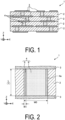
- FIG. 1 is a cross-sectional view illustrating an example of the wiring board 1 according to the embodiment.
- the wiring board 1 according to the embodiment includes an insulation layer 2, an electrical conductor layer 3, and a via conductor 4.
- the insulation layer 2 is made of one ceramic selected from the group consisting of, for example, a glass ceramic sintered body, an aluminum oxide sintered body, an aluminum nitride sintered body, a silicon carbide sintered body, a silicon nitride sintered body, and a mullite sintered body.
- the insulation layer 2 may be made of, for example, a glass ceramic.
- a green sheet that is the raw material of the insulation layer 2 and an electrically conductive paste that is the raw material of the electrical conductor layer 3 and the via conductor 4 are simultaneously fired to manufacture the wiring board 1.
- the manufacturing cost of the wiring board 1 can be reduced.
- the wiring board 1 is configured by layering a plurality of (four in the drawing) insulation layers 2. Note that, in the present disclosure, the wiring board 1 may be constituted by one insulation layer 2.
- the electrical conductor layer 3 has electrical conductivity and is disposed in a predetermined pattern shape on a surface of the insulation layer 2 and between the insulation layers 2 adjacent to each other. That is, in the wiring board 1, the insulation layer 2 and the electrical conductor layer 3 are alternately layered.
- the electrical conductor layer 3 is made of a metal material such as copper, silver, palladium, gold, platinum, tungsten, molybdenum, or manganese, or a mixed material typified by an alloy material or an intermetallic compound containing the metal material as a main component.
- the via conductor 4 has conductivity and is disposed passing through the insulation layer 2 in a thickness direction of the insulation layer 2.
- the via conductor 4 includes a metal portion 7 (refer to FIG. 5 ) and ceramic portions 8 (refer to FIG. 5 ).
- the metal portion 7 is made of a metal and, for example, is made of copper, silver, palladium, gold, platinum-tungsten, molybdenum, or manganese.
- the metal portion 7 may be made of, for example, copper.
- the via conductor 4 can have enhanced electrical conductivity.
- the ceramic portion 8 is made of ceramic.
- the ceramic portion 8 may be made of, for example, the same material as at least one of the ceramic materials included in the insulation layer 2.
- the behaviors of thermal shrinkage of the insulation layer 2 and the via conductor 4 can be brought close to each other, and damage to the wiring board 1 due to thermal shrinkage in the simultaneous firing treatment of the wiring board 1 can be reduced.
- FIG. 2 is a vertical cross-sectional view illustrating an example of the configuration of the via conductor 4 according to the embodiment
- FIG. 3 is a horizontal cross-sectional view illustrating the example of the configuration of the via conductor 4 according to the embodiment.
- the via conductor 4 has a pillar shape such as, for example, a substantially cylindrical shape.
- the via conductor 4 includes a continuous phase 5 and a core portion 6.
- the continuous phase 5 is disposed along a side surface 4a of the via conductor 4 having a pillar shape, and has a predetermined thickness from the side surface 4a toward a center. That is, as illustrated in FIG. 2 , the continuous phase 5 has a strip shape having a length L corresponding to a thickness T of the insulation layer 2 in a vertical cross-sectional view.
- FIG. 4 is a diagram illustrating an example of an arrangement of crystallites 9 in the via conductor 4 according to the embodiment.
- the continuous phase 5 multiple crystallites 9 of metal particles constituting the metal portion 7 (refer to FIG. 5 ) are present, and the crystallites 9 are continuously connected. That is, the metal portion 7 included in the via conductor 4 includes the continuous phase 5 having a strip shape in a vertical cross-sectional view in the vicinity of the side surface 4a (refer to FIG. 2 ) of the via conductor 4.
- the crystallites 9 of the metal particles include those having polygonal shapes in a cross-sectional view. As illustrated in FIG. 4 , the plurality of crystallites 9 are in contact with one another at linear sides of the crystallites 9 having polygonal shapes. In the metal portion 7 formed by the crystallites 9 having such polygonal shapes, the crystallites 9 are integrally connected to one another without gaps such as voids or foreign matter such as ceramic particles interposed therebetween.
- the continuous phase 5 having a strip shape basically refers to a so-called rectangular shape (or oblong shape) having a length equal to that of the thickness direction of the insulation layer 2 as illustrated in FIG. 2 in a vertical cross-sectional view of the via conductor 4, but is not limited thereto, and is intended to include a case in which both side surfaces of the continuous phase 5 have uneven shapes.
- the unevenness is caused by outer shapes of the particles constituting the metal portion 7 and/or the ceramic portions 8 included in the via conductor 4. Accordingly, when an average roughness Ra of both side surfaces of the continuous phase 5 is measured, there may be a portion that is smaller than an average particle diameter of the particles (or crystallites) constituting the metal portion 7 and/or the ceramic portions 8 included in the via conductor 4.
- Both side surfaces of the continuous phase 5 refer to a surface in contact with the insulation layer 2 and a surface in contact with the core portion 6.
- one side surface of the continuous phase 5 in the width direction is an interface between the continuous phase 5 and the insulation layer 2.
- the side surface on the opposite side may be provided with the separation line 5A such as illustrated in FIG. 5 .
- the separation line 5A is linearly connecting, in the thickness direction, multiple ceramic portions 8 having particle shapes and included in the via conductor 4. As shown in FIG. 5 , the position where the separation line 5A is drawn at the ceramic portions 8 is on the continuous phase 5 side of the ceramic portions 8 in a vertical cross-sectional view of the via conductor 4.
- the position where the separation line 5A is drawn at the ceramic portions 8 is on the continuous phase 5 side of the ceramic portions 8.
- the position where the separation line 5A is drawn at the ceramic portions 8 is a position of contact with the continuous phase 5 on the left side of the ceramic portions 8.
- the ceramic portions 8 selected have an average particle diameter of 200 (nm) or greater.
- the ceramic portions 8 having a maximum diameter of 200 (nm) or less may be present in the continuous phase 5. However, in the continuous phase 5, a proportion of the ceramic portions 8 is preferably smaller closer to the insulation layer 2, which is an outer peripheral side of the via conductor 4, than that closer to the core portion 6.
- the proportion of the ceramic portions 8 may be a quantity ratio in addition to a volume ratio or an area ratio. This is because a portion close to the insulation layer 2 in the via conductor 4 is a portion where a skin effect is more pronounced at higher frequencies.
- the presence proportion of the ceramic portions 8 is low in the portion of the via conductor 4 near the insulation layer 2.
- the proportion of the ceramic portions 8 is preferably smaller in the portion on the insulation layer 2 side than in the portion on the core portion 6 side.
- these ceramic portions 8 minute in size are also preferably present closer to the core portion 6 than to the insulation layer 2.
- the vicinity of an outer periphery of the via conductor 4 has a phase in which the presence of the ceramic portions 8 minute in size and having a maximum diameter of several (nm) is also not recognized.
- the core portion 6 is disposed on an inner side of the continuous phase 5 in the via conductor 4 having a pillar shape.
- the metal portion 7 and the ceramic portions 8 are mixed.
- the continuous phase 5 disposed along the thickness direction of the insulation layer 2 is disposed in the via conductor 4 through which a current flows in the thickness direction of the insulation layer 2.
- a favorable conductive path can be formed by the continuous phase 5 in the vicinity of the interface between the via conductor 4 and the insulation layer 2.
- the via conductor 4 can have increased interface electrical conductivity.
- the length of the continuous phase 5 may be identical to the thickness T of the insulation layer 2 in a vertical cross-sectional view.
- an even more favorable conductive path can be formed in an inner portion of the via conductor 4 by the continuous phase 5.
- the via conductor 4 can have even further increased interface electrical conductivity.
- W1/WO may be not less than 0.01 and not more than 0.5.
- W1/WO may be not less than 0.01 and not more than 0.5.
- the continuous phase 5 may be disposed at both end portions of the via conductor 4 in the width direction. That is, the embodiment may have a core-shell structure in which the continuous phase 5 is positioned along the interface between the via conductor 4 and the insulation layer 2, and the core portion 6 is positioned on an inner side of the continuous phase 5.
- the electrical conductivity in the vicinity of the interface between the via conductor 4 and the insulation layer 2 can be increased, and thus the interface electrical conductivity of the via conductor 4 in a high-frequency region can be further increased.
- an end portion of the via conductor 4 in the width direction refers to a range having a length of not less than 1 ( ⁇ m) and not more than 10 ( ⁇ m) from an end of the via conductor 4 in the width direction (that is, the side surface 4a of the via conductor 4) toward the inner side of the via conductor 4.
- an area ratio of the metal portion 7 in the inner portion of the via conductor 4 may be 60 (%) or greater.
- the electrical conductivity of the core portion 6 can also be increased in addition to that of the via conductor 4.
- the electrical conductivity of the via conductor 4 as a whole can be increased.
- an upper limit of the area ratio of the metal portion 7 in the inner portion of the via conductor 4 is 100%, but a ceramic component may be included to increase an adhesion between the via conductor 4 and the insulation layer 2. Accordingly, the upper limit of the area ratio of the metal portion 7 in the inner portion of the via conductor 4 may be 99%. Furthermore, to strongly adhering the entire side surface of the via conductor 4 to the insulation layer 2, the upper limit of the area ratio of the metal portion 7 in the via conductor 4 may be 90% or 80%.
- the area ratio of the metal portion 7 in the inner portion of the via conductor 4 is found by A1/A0, where A0 is an area of a region obtained by observing the via conductor 4 in a vertical cross-sectional view and A1 is an area of the metal portion 7 occupying that region.
- the continuous phase 5 of the via conductor 4 may contain a silicon oxide component 10 (refer to FIG. 7 ) having a size of not less than 10 (nm) and not more than 50 (nm).
- the silicon oxide component 10 can increase the adhesion between the continuous phase 5 and the insulation layer 2 made of ceramic and adjacent to the continuous phase 5.
- the size refers to the maximum diameter of the silicon oxide component 10 viewed in a cross section of the via conductor 4.
- the wiring board 1 can have enhanced reliability.
- this silicon oxide component 10 has a minute size, a decrease in the interface electrical conductivity of the continuous phase 5 can be reduced.
- the continuous phase 5 may include the crystallites 9 having polygonal shapes. Then, in the embodiment, the crystallites 9 adjacent to one another may be in contact with each other at the sides of the crystallites 9 forming linear shapes as grain boundaries.
- the crystallites 9 having a size of not less than 0.5 ( ⁇ m) and not more than 6.0 ( ⁇ m) preferably account for 90 (%) or more in terms of a quantity ratio.
- the crystallites 9 having polygonal shapes are crystallites in which the number of sides forming linear shapes is two or more.
- the crystallites 9 can be observed by analyzing a polished surface by using an electron back scattered diffraction pattern (EBSD) method, for example.
- EBSD electron back scattered diffraction pattern
- a relative permittivity of the insulation layer 2 may be not less than 5 and not more than 7.
- the via conductor 4 can have increased interface electrical conductivity.
- the wiring boards 1 of an example and a comparative example were fabricated, and differences in various characteristics were evaluated.
- a mixture of 40 (wt.%) of alumina particles and 60 (wt.%) of borosilicate glass was prepared as a material of the insulation layer 2.
- Such a mixture is a glass ceramic raw material having a firing temperature of 900 (°C) or higher and 1000 (°C) or lower.
- an organic binder 20 (parts by mass) of isobutyl methacrylate resin and dibutyl phthalate were used per 100 (parts by mass) of the glass ceramic raw material, and a green sheet having a thickness of 100 ( ⁇ m) was produced by doctor blade molding.
- copper powder having an average particle diameter of 2 ( ⁇ m), borosilicate glass powder having an average particle diameter of 2 ( ⁇ m), and silica (silicon oxide) particles having an average particle diameter of 20 (nm) were prepared.
- the silica particles had a proportion of the integrated amount of the lower limit of 10 (nm) and the upper limit of 30 (nm) of 70 (%) or more.
- the copper powder used had a purity of 99.9%.
- a mixed solvent of isobutyl methacrylate resin, butyl carbitol acetate, and dibutyl phthalate was used as the organic binder.
- a conductive paste containing copper powder, borosilicate glass powder, and silica particles was prepared by adding 5 (parts by mass) of isobutyl methacrylate resin per 100 (parts by mass) of copper powder and further adding a mixed solvent of butyl carbitol acetate and dibutyl phthalate.
- the added amounts of the glass powder and the silica particles shown in Table 1 are each a proportion per 100 parts by mass of copper powder.
- the reason that the added amount of the glass powder in the sample of the comparative example is as large as 20.5 parts by mass is that, in the case of a via conductor in the related art, a gap is likely to be formed between the via conductor and the insulation layer 2 formed after firing unless a conductor paste to which this amount of the glass powder is added is used.
- the conductive paste of the example contains fine silica particles, the added amount of the glass powder can be reduced.
- the via conductor 4 having a filling rate high enough for the metal portion 7 to form the continuous phase 5 can be formed.
- the silica particles may be confirmed as present in the via conductor 4 even after the firing.
- the area ratio of the silica particles in the cross section of the via conductor 4 is about as much as from 0.002 (%) to 0.01 (%). Further, the area ratio of the glass phase in the cross section of the via conductor 4 is about 10 times the area ratio of the silica particles, and is, for example, from 0.02 (%) to 0.1 (%). Thus, the remaining portion in the via conductor 4 is constituted by the metal portion 7 and the ceramic portions 8.
- the ceramic portion 8 is a glass ceramic containing, as a precursor, alumina particles and borosilicate glass originally contained in the green sheet for forming the insulation layer 2 after firing. This glass ceramic conceivably moves from the insulation layer 2 side to the via conductor 4 side during firing.
- Through-holes were formed in advance in the fabricated green sheet, and the through-holes were filled with the conductor paste by a screen printing method. That is, a conductive paste having a substantially cylindrical shape was printed, extending through the green sheet. The conductive paste was printed with predetermined surface areas on both surfaces of the fabricated green sheet including the through-holes and fired. Thus, a wiring conductor according to the example was yielded.
- Such a firing treatment was performed in a reducing atmosphere using a nitrogenhydrogen mixed gas at a maximum temperature of 930 (°C) and a holding time of two (hours).
- a plurality of green sheets were layered to a thickness of 500 ( ⁇ m).
- the wiring board 1 according to the comparative example was fabricated in the same and/or similar manner as the wiring board 1 according to the example described above except that the silica particles were not added to the electrically conductive paste.
- the mixing ratios of the borosilicate glass powder and the silica particles in the electrically conductive paste are the values shown in Table 1 below, and are values appropriately adjusted so that the wiring board 1 was not damaged after the firing treatment.
- the wiring board 1 in comparison with the comparative example in which fine silica particles are not included in the electrically conductive paste, in the example in which the silica particles are included, even when the proportion of the borosilicate glass powder is decreased (that is, the proportion of the copper powder is increased), the wiring board 1 can be formed without being damaged at the time of firing.
- the reason for this is presumably as follows. Before the firing treatment, the silica particles of the fine powder adhere to the periphery of the copper powder, whereby a necking start temperature of the copper powder is shifted to a high temperature side. Thus, the necking start temperature of the copper powder that is the main component of the via conductor 4 can be aligned with a necking start temperature of the glass ceramic powder that is the main component of the insulation layer 2.
- the via conductor in the related art was fabricated by adding 20.5 parts by mass of borosilicate glass powder.
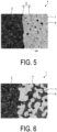
- FIG. 5 and FIG. 7 are diagrams showing SEM observation photographs of the via conductor 4 according to the example, and FIG. 6 is a diagram showing an SEM observation photograph of the via conductor 4 of the comparative example.
- the continuous phase 5 disposed along the thickness direction of the insulation layer 2 was present in the via conductor 4.
- the continuous phase 5 had a strip shape and the length L (refer to FIG. 2 ) corresponding to the thickness T (refer to FIG. 2 ) of the insulation layer 2.
- the average width WO (refer to FIG. 2 ) of the via conductor 4 was approximately 80 ( ⁇ m)
- the average width W1 (refer to FIG. 2 ) of the continuous phase 5 was approximately 2 ( ⁇ m).
- the range of the continuous phase 5 having a strip shape was determined by adding the separation line 5A to the via conductor 4 imaged in the SEM observation photograph as shown in FIG. 5 .
- the reason that the continuous phase 5 having the strip shape was formed in the via conductor 4 is presumably as follows.
- the copper powder of the via conductor 4 in contact with the glass ceramic powder of the green sheet has a reduced apparent melting point compared with that of the copper powder of other sites.
- the continuous phase 5 having a strip shape is formed.
- the silicon oxide component 10 was observed between the crystallites 9 made of copper and adjacent to each other in the continuous phase 5. Such a silicon oxide component 10 is presumably caused by the silica particles of the fine powder.
- the proportion (area ratio) of the metal portion 7 in the via conductor 4 as a whole was obtained using SEM observation photographs of the via conductor 4 for each of the example and the comparative example. Specifically, each obtained SEM observation photograph was converted into a binary image having a predetermined brightness (for example, a brightness of 50%) or greater and less than a predetermined brightness, and the ratio of the number of pixels having the predetermined brightness or greater to the total number of pixels in the binary image was calculated to obtain the area ratio of the metal portion 7.
- a predetermined brightness for example, a brightness of 50%
- the method of measuring interface electrical conductivity by using the cylindrical dielectric resonator method is a method of measuring electrical conductivity at the interface between a conductor and an insulation layer, i.e., at the conductor interface, by attaching an insulation layer having the conductor formed therein to both end faces or one end face of a dielectric cylinder made of a dielectric material having known relative permittivity and dielectric loss such that a predetermined relationship is established and thereby forming a dielectric resonator.
- the principle of this measurement method is based on the fact that when conductor plates large enough to ignore a cut-edge effect (usually, conductor plates having a diameter D of about three times a diameter d of the dielectric cylinder) are placed in parallel on both end surfaces of the dielectric cylinder having a predetermined dimensional ratio (height h/diameter d) and supported thereon to form an electromagnetic field resonator, a high-frequency current flowing through the conductor plates in the TEomn resonance mode (hereinafter, referred to as the TEomn mode) is distributed only on the short-circuited surface, i.e., the facing surface between the dielectric body and the conductor.
- the TEomn mode a high-frequency current flowing through the conductor plates in the TEomn resonance mode
- the interface electrical conductivity was measured at a frequency of 6 (GHz).
- Table 1 shows the added amounts of the glass powder and the silica particles contained in the electrically conductive paste as the material of the via conductor 4, the measurement results of the interface electrical conductivity at the frequency of 6 GHz, and the measurement results of the proportion of the metal portion 7 in the via conductor 4 for the example and the comparative example. Note that the measurement result of the interface electrical conductivity at a frequency of 6 (GHz) is a relative value given 100 (%) as the interface electrical conductivity with direct current.
- the proportion of the metal portion 7 can be increased to 60 (%) or more by adding silica particles to the electrically conductive paste.
- ceramic fine powder other than silica for example, alumina fine powder
- alumina fine powder may be added to the electrically conductive paste.
- the same and/or similar effects as those in the embodiment described above can be obtained.
- the adhesion between the insulation layer 2 and the via conductor 4 can be improved by using the fine powder of silica particles, which is the same component as the component contained in the glass ceramic (here, borosilicate glass) of the insulation layer 2, which can enhance the reliability of the wiring board 1.
Landscapes
- Engineering & Computer Science (AREA)
- Microelectronics & Electronic Packaging (AREA)
- Chemical & Material Sciences (AREA)
- Ceramic Engineering (AREA)
- Manufacturing & Machinery (AREA)
- Inorganic Chemistry (AREA)
- Materials Engineering (AREA)
- Structural Engineering (AREA)
- Organic Chemistry (AREA)
- Production Of Multi-Layered Print Wiring Board (AREA)
- Printing Elements For Providing Electric Connections Between Printed Circuits (AREA)
Abstract
Description
- An embodiment of the present disclosure relates to a wiring board.
- A known wiring board includes an insulation layer, an electrical conductor layer containing copper as a main component, and a via conductor. Such a wiring board is obtained by, for example, simultaneously firing an electrical conductor material, obtained by adding a metal oxide to copper powder, and a glass ceramic as an insulation layer material (refer to
Patent Document 1, for example). - Patent Document 1:
JP 2003-277852 A - According to an aspect of the present disclosure, a wiring board includes an insulation layer made of ceramic, and a via conductor extending through the insulation layer in a thickness direction. The via conductor includes a metal portion and a ceramic portion. The metal portion includes a continuous phase disposed along the thickness direction of the insulation layer in a vertical cross-sectional view.
-
- FIG. 1 is a cross-sectional view illustrating an example of a configuration of a wiring board according to an embodiment.
- FIG. 2 is a vertical cross-sectional view illustrating an example of a configuration of a via conductor according to the embodiment.
- FIG. 3 is a horizontal cross-sectional view illustrating the example of the configuration of the via conductor according to the embodiment.
- FIG. 4 is a diagram illustrating an example of an arrangement of a crystallite in the via conductor according to the embodiment.
- FIG. 5 is a diagram showing an SEM observation photograph of the via conductor according to an example.
- FIG. 6 is a diagram showing an SEM observation photograph of the via conductor in a comparative example.
- FIG. 7 is a diagram showing an SEM observation photograph of the via conductor according to the example.
- A known wiring board includes an insulation layer, an electrical conductor layer containing copper as a main component, and a via conductor. Such a wiring board is obtained by, for example, simultaneously firing an electrical conductor material, obtained by adding a metal oxide to copper powder, and a glass ceramic as an insulation layer material.
- However, in the related art, there is room for further improvement in increasing an interface electrical conductivity of the via conductor.
- As such, a technique that can overcome the aforementioned problem and increase the interface electrical conductivity of the via conductor has yet to be realized.
- Hereinafter, embodiments of a wiring board disclosed in the present disclosure will be described with reference to the accompanying drawings. Note that the present invention is not limited by the following embodiments. In the following description, in order to clarify a positional relationship, an X axis, a Y axis, and a Z axis orthogonal to one another are defined, and a Z-axis direction is a thickness direction of an insulation layer.
- First, a configuration of a
wiring board 1 according to an embodiment will be described with reference toFIG. 1. FIG. 1 is a cross-sectional view illustrating an example of thewiring board 1 according to the embodiment. As illustrated inFIG. 1 , thewiring board 1 according to the embodiment includes aninsulation layer 2, anelectrical conductor layer 3, and avia conductor 4. - The
insulation layer 2 is made of one ceramic selected from the group consisting of, for example, a glass ceramic sintered body, an aluminum oxide sintered body, an aluminum nitride sintered body, a silicon carbide sintered body, a silicon nitride sintered body, and a mullite sintered body. - The
insulation layer 2 may be made of, for example, a glass ceramic. Thus, a green sheet that is the raw material of theinsulation layer 2 and an electrically conductive paste that is the raw material of theelectrical conductor layer 3 and thevia conductor 4 are simultaneously fired to manufacture thewiring board 1. Thus, according to the embodiment, the manufacturing cost of thewiring board 1 can be reduced. - For example, as illustrated in
FIG. 1 , thewiring board 1 according to the embodiment is configured by layering a plurality of (four in the drawing)insulation layers 2. Note that, in the present disclosure, thewiring board 1 may be constituted by oneinsulation layer 2. - The
electrical conductor layer 3 has electrical conductivity and is disposed in a predetermined pattern shape on a surface of theinsulation layer 2 and between theinsulation layers 2 adjacent to each other. That is, in thewiring board 1, theinsulation layer 2 and theelectrical conductor layer 3 are alternately layered. - The
electrical conductor layer 3 is made of a metal material such as copper, silver, palladium, gold, platinum, tungsten, molybdenum, or manganese, or a mixed material typified by an alloy material or an intermetallic compound containing the metal material as a main component. - The
via conductor 4 has conductivity and is disposed passing through theinsulation layer 2 in a thickness direction of theinsulation layer 2. Thevia conductor 4 includes a metal portion 7 (refer toFIG. 5 ) and ceramic portions 8 (refer toFIG. 5 ). - The
metal portion 7 is made of a metal and, for example, is made of copper, silver, palladium, gold, platinum-tungsten, molybdenum, or manganese. Themetal portion 7 may be made of, for example, copper. Thus, thevia conductor 4 can have enhanced electrical conductivity. - The
ceramic portion 8 is made of ceramic. Theceramic portion 8 may be made of, for example, the same material as at least one of the ceramic materials included in theinsulation layer 2. - Thus, the behaviors of thermal shrinkage of the
insulation layer 2 and thevia conductor 4 can be brought close to each other, and damage to thewiring board 1 due to thermal shrinkage in the simultaneous firing treatment of thewiring board 1 can be reduced. - Details of the
via conductor 4 according to the embodiment will be described with reference toFIG. 2 to FIG. 4 .FIG. 2 is a vertical cross-sectional view illustrating an example of the configuration of thevia conductor 4 according to the embodiment, andFIG. 3 is a horizontal cross-sectional view illustrating the example of the configuration of thevia conductor 4 according to the embodiment. - As illustrated in
FIG. 2 andFIG. 3 , thevia conductor 4 has a pillar shape such as, for example, a substantially cylindrical shape. Thevia conductor 4 includes acontinuous phase 5 and acore portion 6. - The
continuous phase 5 is disposed along aside surface 4a of thevia conductor 4 having a pillar shape, and has a predetermined thickness from theside surface 4a toward a center. That is, as illustrated inFIG. 2 , thecontinuous phase 5 has a strip shape having a length L corresponding to a thickness T of theinsulation layer 2 in a vertical cross-sectional view. -
FIG. 4 is a diagram illustrating an example of an arrangement ofcrystallites 9 in thevia conductor 4 according to the embodiment. As illustrated inFIG. 4 , in thecontinuous phase 5,multiple crystallites 9 of metal particles constituting the metal portion 7 (refer toFIG. 5 ) are present, and thecrystallites 9 are continuously connected. That is, themetal portion 7 included in thevia conductor 4 includes thecontinuous phase 5 having a strip shape in a vertical cross-sectional view in the vicinity of theside surface 4a (refer toFIG. 2 ) of thevia conductor 4. - Here, the
crystallites 9 of the metal particles include those having polygonal shapes in a cross-sectional view. As illustrated inFIG. 4 , the plurality ofcrystallites 9 are in contact with one another at linear sides of thecrystallites 9 having polygonal shapes. In themetal portion 7 formed by thecrystallites 9 having such polygonal shapes, thecrystallites 9 are integrally connected to one another without gaps such as voids or foreign matter such as ceramic particles interposed therebetween. - A method for determining a region of the
continuous phase 5 having a strip shape will be described below. Note that the following method for identifying aseparation line 5A (refer toFIG. 5 ) is merely an example. Thecontinuous phase 5 having a strip shape basically refers to a so-called rectangular shape (or oblong shape) having a length equal to that of the thickness direction of theinsulation layer 2 as illustrated inFIG. 2 in a vertical cross-sectional view of thevia conductor 4, but is not limited thereto, and is intended to include a case in which both side surfaces of thecontinuous phase 5 have uneven shapes. - In this case, the unevenness is caused by outer shapes of the particles constituting the
metal portion 7 and/or theceramic portions 8 included in thevia conductor 4. Accordingly, when an average roughness Ra of both side surfaces of thecontinuous phase 5 is measured, there may be a portion that is smaller than an average particle diameter of the particles (or crystallites) constituting themetal portion 7 and/or theceramic portions 8 included in the viaconductor 4. - Both side surfaces of the
continuous phase 5 refer to a surface in contact with theinsulation layer 2 and a surface in contact with thecore portion 6. When a portion of thecontinuous phase 5 is specified in the viaconductor 4, one side surface of thecontinuous phase 5 in the width direction is an interface between thecontinuous phase 5 and theinsulation layer 2. The side surface on the opposite side (side surface on the other side) may be provided with theseparation line 5A such as illustrated inFIG. 5 . - In this case, the
separation line 5A is linearly connecting, in the thickness direction, multipleceramic portions 8 having particle shapes and included in the viaconductor 4. As shown inFIG. 5 , the position where theseparation line 5A is drawn at theceramic portions 8 is on thecontinuous phase 5 side of theceramic portions 8 in a vertical cross-sectional view of the viaconductor 4. - That is, the position where the
separation line 5A is drawn at theceramic portions 8 is on thecontinuous phase 5 side of theceramic portions 8. InFIG. 5 , the position where theseparation line 5A is drawn at theceramic portions 8 is a position of contact with thecontinuous phase 5 on the left side of theceramic portions 8. In this case, theceramic portions 8 selected have an average particle diameter of 200 (nm) or greater. - The
ceramic portions 8 having a maximum diameter of 200 (nm) or less may be present in thecontinuous phase 5. However, in thecontinuous phase 5, a proportion of theceramic portions 8 is preferably smaller closer to theinsulation layer 2, which is an outer peripheral side of the viaconductor 4, than that closer to thecore portion 6. - Here, the proportion of the
ceramic portions 8 may be a quantity ratio in addition to a volume ratio or an area ratio. This is because a portion close to theinsulation layer 2 in the viaconductor 4 is a portion where a skin effect is more pronounced at higher frequencies. - Thus, preferably the presence proportion of the
ceramic portions 8 is low in the portion of the viaconductor 4 near theinsulation layer 2. For example, when thecontinuous phase 5 is divided into two equal parts in the width direction between the interface with theinsulation layer 2 and theseparation line 5A, the proportion of theceramic portions 8 is preferably smaller in the portion on theinsulation layer 2 side than in the portion on thecore portion 6 side. - For example, as illustrated in
FIG. 5 , even for theceramic portions 8 minute in size and having a maximum diameter of several (nm) in thecontinuous phase 5, theseceramic portions 8 minute in size are also preferably present closer to thecore portion 6 than to theinsulation layer 2. Preferably, the vicinity of an outer periphery of the viaconductor 4 has a phase in which the presence of theceramic portions 8 minute in size and having a maximum diameter of several (nm) is also not recognized. - As illustrated in
FIG. 2 andFIG. 3 , thecore portion 6 is disposed on an inner side of thecontinuous phase 5 in the viaconductor 4 having a pillar shape. In thecore portion 6, themetal portion 7 and the ceramic portions 8 (refer toFIG. 5 ) are mixed. - As described above, in the embodiment, the
continuous phase 5 disposed along the thickness direction of theinsulation layer 2 is disposed in the viaconductor 4 through which a current flows in the thickness direction of theinsulation layer 2. Thus, a favorable conductive path can be formed by thecontinuous phase 5 in the vicinity of the interface between the viaconductor 4 and theinsulation layer 2. - Thus, according to the embodiment, the via
conductor 4 can have increased interface electrical conductivity. - Further, in the embodiment, the length of the
continuous phase 5 may be identical to the thickness T of theinsulation layer 2 in a vertical cross-sectional view. Thus, an even more favorable conductive path can be formed in an inner portion of the viaconductor 4 by thecontinuous phase 5. - Thus, according to the embodiment, the via
conductor 4 can have even further increased interface electrical conductivity. - In the embodiment, as illustrated in
FIG. 2 , given WO as an average width of the viaconductor 4 and W1 as an average width of thecontinuous phase 5, W1/WO may be not less than 0.01 and not more than 0.5. Thus, the width by which thecontinuous phase 5 extends through theinsulation layer 2 in the thickness direction can be increased, and thus the interface electrical conductivity of the viaconductor 4 can be further increased. - In the embodiment, as illustrated in
FIG. 2 , in a vertical cross-sectional view of the viaconductor 4, thecontinuous phase 5 may be disposed at both end portions of the viaconductor 4 in the width direction. That is, the embodiment may have a core-shell structure in which thecontinuous phase 5 is positioned along the interface between the viaconductor 4 and theinsulation layer 2, and thecore portion 6 is positioned on an inner side of thecontinuous phase 5. - Thus, the electrical conductivity in the vicinity of the interface between the via
conductor 4 and theinsulation layer 2 can be increased, and thus the interface electrical conductivity of the viaconductor 4 in a high-frequency region can be further increased. - Note that, in the present disclosure, an end portion of the via
conductor 4 in the width direction refers to a range having a length of not less than 1 (µm) and not more than 10 (µm) from an end of the viaconductor 4 in the width direction (that is, theside surface 4a of the via conductor 4) toward the inner side of the viaconductor 4. - Further, in the embodiment, an area ratio of the
metal portion 7 in the inner portion of the viaconductor 4 may be 60 (%) or greater. Thus, the electrical conductivity of thecore portion 6 can also be increased in addition to that of the viaconductor 4. As a result, the electrical conductivity of the viaconductor 4 as a whole can be increased. - Note that, in this case, an upper limit of the area ratio of the
metal portion 7 in the inner portion of the viaconductor 4 is 100%, but a ceramic component may be included to increase an adhesion between the viaconductor 4 and theinsulation layer 2. Accordingly, the upper limit of the area ratio of themetal portion 7 in the inner portion of the viaconductor 4 may be 99%. Furthermore, to strongly adhering the entire side surface of the viaconductor 4 to theinsulation layer 2, the upper limit of the area ratio of themetal portion 7 in the viaconductor 4 may be 90% or 80%. - Note that, in the present disclosure, the area ratio of the
metal portion 7 in the inner portion of the viaconductor 4 is found by A1/A0, where A0 is an area of a region obtained by observing the viaconductor 4 in a vertical cross-sectional view and A1 is an area of themetal portion 7 occupying that region. - In the embodiment, the
continuous phase 5 of the viaconductor 4 may contain a silicon oxide component 10 (refer toFIG. 7 ) having a size of not less than 10 (nm) and not more than 50 (nm). Thus, thesilicon oxide component 10 can increase the adhesion between thecontinuous phase 5 and theinsulation layer 2 made of ceramic and adjacent to thecontinuous phase 5. Herein, the size refers to the maximum diameter of thesilicon oxide component 10 viewed in a cross section of the viaconductor 4. - Thus, according to the embodiment, the
wiring board 1 can have enhanced reliability. In the embodiment, because thissilicon oxide component 10 has a minute size, a decrease in the interface electrical conductivity of thecontinuous phase 5 can be reduced. - In the embodiment, as illustrated in
FIG. 4 , thecontinuous phase 5 may include thecrystallites 9 having polygonal shapes. Then, in the embodiment, thecrystallites 9 adjacent to one another may be in contact with each other at the sides of thecrystallites 9 forming linear shapes as grain boundaries. - Thus, even when the
silicon oxide component 10 minute in size is present at the interface between thecrystallites 9, a contact surface area between thecrystallites 9 can be increased. As a result, the interface electrical conductivity of the viaconductor 4 in a high frequency region can be increased. - In the embodiment, the
crystallites 9 having a size of not less than 0.5 (µm) and not more than 6.0 (µm) preferably account for 90 (%) or more in terms of a quantity ratio. - Note that, in the present disclosure, the
crystallites 9 having polygonal shapes are crystallites in which the number of sides forming linear shapes is two or more. In the present disclosure, thecrystallites 9 can be observed by analyzing a polished surface by using an electron back scattered diffraction pattern (EBSD) method, for example. - In the embodiment, a relative permittivity of the
insulation layer 2 may be not less than 5 and not more than 7. Thus, the viaconductor 4 can have increased interface electrical conductivity. - Specifically, the
wiring boards 1 of an example and a comparative example were fabricated, and differences in various characteristics were evaluated. - As the embodiment, first, a mixture of 40 (wt.%) of alumina particles and 60 (wt.%) of borosilicate glass was prepared as a material of the
insulation layer 2. Such a mixture is a glass ceramic raw material having a firing temperature of 900 (°C) or higher and 1000 (°C) or lower. - As an organic binder, 20 (parts by mass) of isobutyl methacrylate resin and dibutyl phthalate were used per 100 (parts by mass) of the glass ceramic raw material, and a green sheet having a thickness of 100 (µm) was produced by doctor blade molding.
- As raw materials of the via
conductor 4, copper powder having an average particle diameter of 2 (µm), borosilicate glass powder having an average particle diameter of 2 (µm), and silica (silicon oxide) particles having an average particle diameter of 20 (nm) were prepared. The silica particles had a proportion of the integrated amount of the lower limit of 10 (nm) and the upper limit of 30 (nm) of 70 (%) or more. The copper powder used had a purity of 99.9%. - As the organic binder, a mixed solvent of isobutyl methacrylate resin, butyl carbitol acetate, and dibutyl phthalate was used. A conductive paste containing copper powder, borosilicate glass powder, and silica particles was prepared by adding 5 (parts by mass) of isobutyl methacrylate resin per 100 (parts by mass) of copper powder and further adding a mixed solvent of butyl carbitol acetate and dibutyl phthalate.
- The added amounts of the glass powder and the silica particles shown in Table 1 are each a proportion per 100 parts by mass of copper powder.
- Note that the reason that the added amount of the glass powder in the sample of the comparative example is as large as 20.5 parts by mass is that, in the case of a via conductor in the related art, a gap is likely to be formed between the via conductor and the
insulation layer 2 formed after firing unless a conductor paste to which this amount of the glass powder is added is used. - That is, because the conductive paste of the example contains fine silica particles, the added amount of the glass powder can be reduced. Thus, even with a composition containing a small added amount of glass powder as illustrated in the example, the via
conductor 4 having a filling rate high enough for themetal portion 7 to form thecontinuous phase 5 can be formed. - In this case, the silica particles may be confirmed as present in the via
conductor 4 even after the firing. - The area ratio of the silica particles in the cross section of the via
conductor 4 is about as much as from 0.002 (%) to 0.01 (%). Further, the area ratio of the glass phase in the cross section of the viaconductor 4 is about 10 times the area ratio of the silica particles, and is, for example, from 0.02 (%) to 0.1 (%). Thus, the remaining portion in the viaconductor 4 is constituted by themetal portion 7 and theceramic portions 8. - The
ceramic portion 8 is a glass ceramic containing, as a precursor, alumina particles and borosilicate glass originally contained in the green sheet for forming theinsulation layer 2 after firing. This glass ceramic conceivably moves from theinsulation layer 2 side to the viaconductor 4 side during firing. - Through-holes were formed in advance in the fabricated green sheet, and the through-holes were filled with the conductor paste by a screen printing method. That is, a conductive paste having a substantially cylindrical shape was printed, extending through the green sheet. The conductive paste was printed with predetermined surface areas on both surfaces of the fabricated green sheet including the through-holes and fired. Thus, a wiring conductor according to the example was yielded.
- Such a firing treatment was performed in a reducing atmosphere using a nitrogenhydrogen mixed gas at a maximum temperature of 930 (°C) and a holding time of two (hours). A plurality of green sheets were layered to a thickness of 500 (µm).
- On the other hand, the
wiring board 1 according to the comparative example was fabricated in the same and/or similar manner as thewiring board 1 according to the example described above except that the silica particles were not added to the electrically conductive paste. Note that, in the example and the comparative example, the mixing ratios of the borosilicate glass powder and the silica particles in the electrically conductive paste are the values shown in Table 1 below, and are values appropriately adjusted so that thewiring board 1 was not damaged after the firing treatment. - Here, as shown in Table 1, in comparison with the comparative example in which fine silica particles are not included in the electrically conductive paste, in the example in which the silica particles are included, even when the proportion of the borosilicate glass powder is decreased (that is, the proportion of the copper powder is increased), the
wiring board 1 can be formed without being damaged at the time of firing. - The reason for this is presumably as follows. Before the firing treatment, the silica particles of the fine powder adhere to the periphery of the copper powder, whereby a necking start temperature of the copper powder is shifted to a high temperature side. Thus, the necking start temperature of the copper powder that is the main component of the via
conductor 4 can be aligned with a necking start temperature of the glass ceramic powder that is the main component of theinsulation layer 2. - Accordingly, in the example, by including the fine silica particles in the electrically conductive paste, even when the proportion of the borosilicate glass powder is reduced, the breakage caused by the thermal shrinkage after the firing treatment can be reduced. As shown as the comparative example in Table 1, the via conductor in the related art was fabricated by adding 20.5 parts by mass of borosilicate glass powder.
- The obtained
wiring board 1 was then cut, and the interface between theinsulation layer 2 and the viaconductor 4 as well as the vicinity thereof were observed with a scanning electron microscope (SEM).FIG. 5 andFIG. 7 are diagrams showing SEM observation photographs of the viaconductor 4 according to the example, andFIG. 6 is a diagram showing an SEM observation photograph of the viaconductor 4 of the comparative example. - As shown in
FIG. 5 , in the example, thecontinuous phase 5 disposed along the thickness direction of theinsulation layer 2 was present in the viaconductor 4. Thecontinuous phase 5 had a strip shape and the length L (refer toFIG. 2 ) corresponding to the thickness T (refer toFIG. 2 ) of theinsulation layer 2. - Note that, in the example, the average width WO (refer to
FIG. 2 ) of the viaconductor 4 was approximately 80 (µm), and the average width W1 (refer toFIG. 2 ) of thecontinuous phase 5 was approximately 2 (µm). The range of thecontinuous phase 5 having a strip shape was determined by adding theseparation line 5A to the viaconductor 4 imaged in the SEM observation photograph as shown inFIG. 5 . - On the other hand, as shown in
FIG. 6 , in the comparative example, thecontinuous phase 5 having a strip shape was not observed in the viaconductor 4. - In the
wiring board 1 according to the example, the reason that thecontinuous phase 5 having the strip shape was formed in the viaconductor 4 is presumably as follows. In the firing treatment, the copper powder of the viaconductor 4 in contact with the glass ceramic powder of the green sheet has a reduced apparent melting point compared with that of the copper powder of other sites. - In the copper powder of the via
conductor 4 in contact with the green sheet, because the copper particles are readily formed into a film shape by the silica particles of the fine powder, thecontinuous phase 5 having a strip shape is formed. - As shown in
FIG. 7 , in the viaconductor 4 of thewiring board 1 according to the example, thesilicon oxide component 10 was observed between thecrystallites 9 made of copper and adjacent to each other in thecontinuous phase 5. Such asilicon oxide component 10 is presumably caused by the silica particles of the fine powder. - Further, the proportion (area ratio) of the
metal portion 7 in the viaconductor 4 as a whole was obtained using SEM observation photographs of the viaconductor 4 for each of the example and the comparative example. Specifically, each obtained SEM observation photograph was converted into a binary image having a predetermined brightness (for example, a brightness of 50%) or greater and less than a predetermined brightness, and the ratio of the number of pixels having the predetermined brightness or greater to the total number of pixels in the binary image was calculated to obtain the area ratio of themetal portion 7. - Next, the interface electrical conductivity of the
wiring board 1 in each of the example and the comparative example was measured. This interface electrical conductivity was measured by a cylindrical dielectric resonator method described below. - The method of measuring interface electrical conductivity by using the cylindrical dielectric resonator method is a method of measuring electrical conductivity at the interface between a conductor and an insulation layer, i.e., at the conductor interface, by attaching an insulation layer having the conductor formed therein to both end faces or one end face of a dielectric cylinder made of a dielectric material having known relative permittivity and dielectric loss such that a predetermined relationship is established and thereby forming a dielectric resonator.
- The principle of this measurement method is based on the fact that when conductor plates large enough to ignore a cut-edge effect (usually, conductor plates having a diameter D of about three times a diameter d of the dielectric cylinder) are placed in parallel on both end surfaces of the dielectric cylinder having a predetermined dimensional ratio (height h/diameter d) and supported thereon to form an electromagnetic field resonator, a high-frequency current flowing through the conductor plates in the TEomn resonance mode (hereinafter, referred to as the TEomn mode) is distributed only on the short-circuited surface, i.e., the facing surface between the dielectric body and the conductor.
- In the dielectric resonator, by using the fact that the high-frequency current flowing through the conductor due to the TEomn mode (m = 1, 2, 3, ..., n = 1, 2, 3, ...) is distributed only at the interface between the conductor and a dielectric board in contact with the dielectric cylinder, interface electrical conductivity can be calculated from the measured resonance frequencies f0 of the TEomn mode (m = 1, 2, 3, ..., n = 1, 2, 3, ...) and no-load Q, Qu. The interface electrical conductivity was measured at a frequency of 6 (GHz).
- Table 1 shows the added amounts of the glass powder and the silica particles contained in the electrically conductive paste as the material of the via
conductor 4, the measurement results of the interface electrical conductivity at the frequency of 6 GHz, and the measurement results of the proportion of themetal portion 7 in the viaconductor 4 for the example and the comparative example. Note that the measurement result of the interface electrical conductivity at a frequency of 6 (GHz) is a relative value given 100 (%) as the interface electrical conductivity with direct current. -
TABLE 1 Example Comparative example Added amount of glass powder 1.0 (parts by mass) 20.5 (parts by mass) Added amount of silica particles 0.3 (parts by mass) Not added Interface electrical conductivity (6 GHz) 82 (%) 20 (%) Proportion (area ratio) of metal portion 92.0 (%) 53.8 (%) - From the comparison between the example in which the
continuous phase 5 having a strip shape is disposed in the viaconductor 4 and the comparative example in which thecontinuous phase 5 is not disposed, it is understood that the interface electrical conductivity in the high frequency region of the viaconductor 4 is increased by thecontinuous phase 5 having a strip shape being disposed in the viaconductor 4. - Further, from the comparison between the example in which silica particles are added to the electrically conductive paste that is the raw material of the via
conductor 4 and the comparative example in which silica particles are not added, the proportion of themetal portion 7 can be increased to 60 (%) or more by adding silica particles to the electrically conductive paste. - The embodiment according to the present invention has been described above. However, the present invention is not limited to the embodiment described above, and various modifications can be made without departing from the essential spirit of the present invention. For example, although an example in which a fine powder of silica (silicon oxide) particles is added to an electrically conductive paste that is a raw material of the via
conductor 4 has been illustrated in the embodiment described above, the present disclosure is not limited to such an example. - For example, ceramic fine powder other than silica (for example, alumina fine powder) may be added to the electrically conductive paste. In this case as well, the same and/or similar effects as those in the embodiment described above can be obtained.
- On the other hand, the adhesion between the
insulation layer 2 and the viaconductor 4 can be improved by using the fine powder of silica particles, which is the same component as the component contained in the glass ceramic (here, borosilicate glass) of theinsulation layer 2, which can enhance the reliability of thewiring board 1. - Additional effects and other aspects can be easily derived by a person skilled in the art. Thus, a wide variety of aspects of the present invention are not limited to the specific details and representative embodiment represented and described above. Accordingly, various changes are possible without departing from the spirit or scope of the general inventive concepts defined by the appended claims and their equivalents.
-
- 1 Wiring board
- 2 Insulation layer
- 3 Electrical conductor layer
- 4 Via conductor
- 5 Continuous phase
- 6 Core portion
- 7 Metal portion
- 8 Ceramic portion
- 9 Crystallite
- 10 Silicon oxide component
- L Length
- T Thickness
- WO, W1 Average width
Claims (9)
- A wiring board comprising:an insulation layer made of ceramic; anda via conductor extending through the insulation layer in a thickness direction, whereinthe via conductor comprises a metal portion and a ceramic portion, andthe metal portion comprises a continuous phase disposed along the thickness direction of the insulation layer in a vertical cross-sectional view.
- The wiring board according to claim 1, wherein a length of the continuous phase is identical to a thickness of the insulation layer in a vertical cross-sectional view.
- The wiring board according to claim 1 or 2, wherein W1/W0 is not less than 0.01 and not more than 0.5, where W0 is an average width of the via conductor and W1 is an average width of the continuous phase.
- The wiring board according to any one of claims 1 to 3, wherein the continuous phase is disposed at both end portions of the via conductor in the width direction in a vertical cross-sectional view of the via conductor.
- The wiring board according to any one of claims 1 to 4, wherein an area ratio of the metal portion in an inner portion of the via conductor is not less than 60 (%) and not more than 99 (%).
- The wiring board according to any one of claims 1 to 5, wherein the continuous phase comprises a silicon oxide component having a size not less than 10 (nm) and not more than 50 (nm).
- The wiring board according to any one of claims 1 to 6, wherein the continuous phase further comprises crystallites having polygonal shapes.
- The wiring board according to any one of claims 1 to 7, wherein the continuous phase is positioned near an interface between the insulation layer and the via conductor, extending along the interface.
- The wiring board according to any one of claims 1 to 8, wherein the metal portion has a core-shell structure with a core portion positioned on an inner side of the continuous phase.
Applications Claiming Priority (2)
| Application Number | Priority Date | Filing Date | Title |
|---|---|---|---|
| JP2021159610 | 2021-09-29 | ||
| PCT/JP2022/035265 WO2023054137A1 (en) | 2021-09-29 | 2022-09-21 | Wiring substrate |
Publications (2)
| Publication Number | Publication Date |
|---|---|
| EP4412410A1 true EP4412410A1 (en) | 2024-08-07 |
| EP4412410A4 EP4412410A4 (en) | 2025-09-03 |
Family
ID=85780678
Family Applications (1)
| Application Number | Title | Priority Date | Filing Date |
|---|---|---|---|
| EP22876004.7A Pending EP4412410A4 (en) | 2021-09-29 | 2022-09-21 | WIRING SUBSTRATE |
Country Status (5)
| Country | Link |
|---|---|
| US (1) | US20250142724A1 (en) |
| EP (1) | EP4412410A4 (en) |
| JP (1) | JP7678889B2 (en) |
| CN (1) | CN118020391A (en) |
| WO (1) | WO2023054137A1 (en) |
Families Citing this family (2)
| Publication number | Priority date | Publication date | Assignee | Title |
|---|---|---|---|---|
| JP2025068374A (en) * | 2023-10-16 | 2025-04-28 | 京セラ株式会社 | Wiring board and semiconductor device |
| WO2026005028A1 (en) * | 2024-06-28 | 2026-01-02 | 京セラ株式会社 | Support member, electrostatic chuck, heater, and plasma treatment device |
Family Cites Families (7)
| Publication number | Priority date | Publication date | Assignee | Title |
|---|---|---|---|---|
| JP4646468B2 (en) * | 2001-09-25 | 2011-03-09 | 京セラ株式会社 | Composition for through conductor |
| JP2003277852A (en) | 2002-03-25 | 2003-10-02 | Kyocera Corp | Copper metallized composition and ceramic wiring board |
| US7611645B2 (en) * | 2005-04-25 | 2009-11-03 | E. I. Du Pont De Nemours And Company | Thick film conductor compositions and the use thereof in LTCC circuits and devices |
| JP4807161B2 (en) * | 2006-06-29 | 2011-11-02 | 株式会社村田製作所 | Multilayer ceramic electronic component and manufacturing method thereof |
| JP4781189B2 (en) * | 2006-07-27 | 2011-09-28 | 京セラ株式会社 | Wiring board |
| KR100997989B1 (en) * | 2008-08-28 | 2010-12-03 | 삼성전기주식회사 | Multilayer ceramic substrate |
| JP6369560B2 (en) * | 2015-04-17 | 2018-08-08 | 株式会社村田製作所 | CERAMIC WIRING BOARD AND CERAMIC WIRING BOARD MANUFACTURING METHOD |
-
2022
- 2022-09-21 JP JP2023551394A patent/JP7678889B2/en active Active
- 2022-09-21 EP EP22876004.7A patent/EP4412410A4/en active Pending
- 2022-09-21 CN CN202280062909.2A patent/CN118020391A/en active Pending
- 2022-09-21 WO PCT/JP2022/035265 patent/WO2023054137A1/en not_active Ceased
- 2022-09-21 US US18/689,496 patent/US20250142724A1/en active Pending
Also Published As
| Publication number | Publication date |
|---|---|
| JPWO2023054137A1 (en) | 2023-04-06 |
| US20250142724A1 (en) | 2025-05-01 |
| EP4412410A4 (en) | 2025-09-03 |
| JP7678889B2 (en) | 2025-05-16 |
| CN118020391A (en) | 2024-05-10 |
| WO2023054137A1 (en) | 2023-04-06 |
Similar Documents
| Publication | Publication Date | Title |
|---|---|---|
| KR101862396B1 (en) | Laminated ceramic electronic parts and fabricating method thereof | |
| JP4507012B2 (en) | Multilayer ceramic substrate | |
| EP4412410A1 (en) | Wiring substrate | |
| KR20130013438A (en) | Laminated ceramic electronic parts | |
| US20140022689A1 (en) | Multi-layered ceramic electronic component and method of manufacturing the same | |
| US20230420182A1 (en) | Coil-component manufacturing method and coil component | |
| JP6632995B2 (en) | Ceramic body and method of manufacturing the same | |
| US7817402B2 (en) | Multilayer ceramic electronic device and method of production of the same | |
| US12598700B2 (en) | Wiring board | |
| JP6314292B1 (en) | Ceramic substrate and manufacturing method thereof | |
| CN106458762B (en) | Ceramic substrate and method of making the same | |
| US20250132096A1 (en) | Multilayer ceramic capacitor and multilayer ceramic capacitor mounting structure | |
| EP4535931A1 (en) | Circuit component | |
| EP4503867A1 (en) | Wiring board | |
| JP5648682B2 (en) | Metal base substrate | |
| EP4286077A1 (en) | Wiring board | |
| KR100241159B1 (en) | Ceramic electronic part | |
| JP2006332236A (en) | Conductive paste, multilayer ceramic electronic component manufacturing method, and multilayer ceramic electronic component | |
| EP4521432A1 (en) | Multilayer electronic component | |
| US20260058066A1 (en) | Multilayer ceramic capacitor | |
| KR102789009B1 (en) | Multi-layer ceramic electronic component | |
| US20250259792A1 (en) | Multilayer ceramic capacitor and manufacturing method of multilayer ceramic capacitor | |
| CN122003727A (en) | Multilayer ceramic capacitors | |
| JP2024132401A (en) | Composite particles, conductive paste, and electronic components | |
| CN117597752A (en) | Laminated ceramic electronic component and method of manufacturing laminated ceramic electronic component |
Legal Events
| Date | Code | Title | Description |
|---|---|---|---|
| STAA | Information on the status of an ep patent application or granted ep patent |
Free format text: STATUS: THE INTERNATIONAL PUBLICATION HAS BEEN MADE |
|
| PUAI | Public reference made under article 153(3) epc to a published international application that has entered the european phase |
Free format text: ORIGINAL CODE: 0009012 |
|
| STAA | Information on the status of an ep patent application or granted ep patent |
Free format text: STATUS: REQUEST FOR EXAMINATION WAS MADE |
|
| 17P | Request for examination filed |
Effective date: 20240304 |
|
| AK | Designated contracting states |
Kind code of ref document: A1 Designated state(s): AL AT BE BG CH CY CZ DE DK EE ES FI FR GB GR HR HU IE IS IT LI LT LU LV MC MK MT NL NO PL PT RO RS SE SI SK SM TR |
|
| DAV | Request for validation of the european patent (deleted) | ||
| DAX | Request for extension of the european patent (deleted) | ||
| REG | Reference to a national code |
Ref country code: DE Ref legal event code: R079 Free format text: PREVIOUS MAIN CLASS: H05K0003400000 Ipc: H05K0001030000 |
|
| A4 | Supplementary search report drawn up and despatched |
Effective date: 20250805 |
|
| RIC1 | Information provided on ipc code assigned before grant |
Ipc: H05K 1/03 20060101AFI20250730BHEP Ipc: H05K 1/02 20060101ALI20250730BHEP Ipc: H05K 1/11 20060101ALI20250730BHEP Ipc: H05K 3/40 20060101ALN20250730BHEP Ipc: H05K 3/46 20060101ALN20250730BHEP Ipc: H05K 3/00 20060101ALN20250730BHEP |