EP4408139A2 - Organische elektrolumineszente vorrichtungen - Google Patents
Organische elektrolumineszente vorrichtungen Download PDFInfo
- Publication number
- EP4408139A2 EP4408139A2 EP24154647.2A EP24154647A EP4408139A2 EP 4408139 A2 EP4408139 A2 EP 4408139A2 EP 24154647 A EP24154647 A EP 24154647A EP 4408139 A2 EP4408139 A2 EP 4408139A2
- Authority
- EP
- European Patent Office
- Prior art keywords
- layer
- transport layer
- electrode
- thickness
- display
- Prior art date
- Legal status (The legal status is an assumption and is not a legal conclusion. Google has not performed a legal analysis and makes no representation as to the accuracy of the status listed.)
- Pending
Links
Images


Classifications
-
- H—ELECTRICITY
- H10—SEMICONDUCTOR DEVICES; ELECTRIC SOLID-STATE DEVICES NOT OTHERWISE PROVIDED FOR
- H10K—ORGANIC ELECTRIC SOLID-STATE DEVICES
- H10K50/00—Organic light-emitting devices
- H10K50/80—Constructional details
- H10K50/85—Arrangements for extracting light from the devices
- H10K50/852—Arrangements for extracting light from the devices comprising a resonant cavity structure, e.g. Bragg reflector pair
-
- H—ELECTRICITY
- H10—SEMICONDUCTOR DEVICES; ELECTRIC SOLID-STATE DEVICES NOT OTHERWISE PROVIDED FOR
- H10K—ORGANIC ELECTRIC SOLID-STATE DEVICES
- H10K50/00—Organic light-emitting devices
- H10K50/10—OLEDs or polymer light-emitting diodes [PLED]
- H10K50/11—OLEDs or polymer light-emitting diodes [PLED] characterised by the electroluminescent [EL] layers
- H10K50/12—OLEDs or polymer light-emitting diodes [PLED] characterised by the electroluminescent [EL] layers comprising dopants
-
- H—ELECTRICITY
- H10—SEMICONDUCTOR DEVICES; ELECTRIC SOLID-STATE DEVICES NOT OTHERWISE PROVIDED FOR
- H10K—ORGANIC ELECTRIC SOLID-STATE DEVICES
- H10K50/00—Organic light-emitting devices
- H10K50/10—OLEDs or polymer light-emitting diodes [PLED]
- H10K50/11—OLEDs or polymer light-emitting diodes [PLED] characterised by the electroluminescent [EL] layers
- H10K50/125—OLEDs or polymer light-emitting diodes [PLED] characterised by the electroluminescent [EL] layers specially adapted for multicolour light emission, e.g. for emitting white light
- H10K50/13—OLEDs or polymer light-emitting diodes [PLED] characterised by the electroluminescent [EL] layers specially adapted for multicolour light emission, e.g. for emitting white light comprising stacked EL layers within one EL unit
-
- H—ELECTRICITY
- H10—SEMICONDUCTOR DEVICES; ELECTRIC SOLID-STATE DEVICES NOT OTHERWISE PROVIDED FOR
- H10K—ORGANIC ELECTRIC SOLID-STATE DEVICES
- H10K50/00—Organic light-emitting devices
- H10K50/10—OLEDs or polymer light-emitting diodes [PLED]
- H10K50/14—Carrier transporting layers
- H10K50/15—Hole transporting layers
-
- H—ELECTRICITY
- H10—SEMICONDUCTOR DEVICES; ELECTRIC SOLID-STATE DEVICES NOT OTHERWISE PROVIDED FOR
- H10K—ORGANIC ELECTRIC SOLID-STATE DEVICES
- H10K50/00—Organic light-emitting devices
- H10K50/10—OLEDs or polymer light-emitting diodes [PLED]
- H10K50/14—Carrier transporting layers
- H10K50/16—Electron transporting layers
-
- H—ELECTRICITY
- H10—SEMICONDUCTOR DEVICES; ELECTRIC SOLID-STATE DEVICES NOT OTHERWISE PROVIDED FOR
- H10K—ORGANIC ELECTRIC SOLID-STATE DEVICES
- H10K50/00—Organic light-emitting devices
- H10K50/10—OLEDs or polymer light-emitting diodes [PLED]
- H10K50/19—Tandem OLEDs
-
- H—ELECTRICITY
- H10—SEMICONDUCTOR DEVICES; ELECTRIC SOLID-STATE DEVICES NOT OTHERWISE PROVIDED FOR
- H10K—ORGANIC ELECTRIC SOLID-STATE DEVICES
- H10K50/00—Organic light-emitting devices
- H10K50/80—Constructional details
- H10K50/805—Electrodes
- H10K50/81—Anodes
-
- H—ELECTRICITY
- H10—SEMICONDUCTOR DEVICES; ELECTRIC SOLID-STATE DEVICES NOT OTHERWISE PROVIDED FOR
- H10K—ORGANIC ELECTRIC SOLID-STATE DEVICES
- H10K50/00—Organic light-emitting devices
- H10K50/80—Constructional details
- H10K50/805—Electrodes
- H10K50/82—Cathodes
-
- H—ELECTRICITY
- H10—SEMICONDUCTOR DEVICES; ELECTRIC SOLID-STATE DEVICES NOT OTHERWISE PROVIDED FOR
- H10K—ORGANIC ELECTRIC SOLID-STATE DEVICES
- H10K50/00—Organic light-emitting devices
- H10K50/80—Constructional details
- H10K50/85—Arrangements for extracting light from the devices
-
- H—ELECTRICITY
- H10—SEMICONDUCTOR DEVICES; ELECTRIC SOLID-STATE DEVICES NOT OTHERWISE PROVIDED FOR
- H10K—ORGANIC ELECTRIC SOLID-STATE DEVICES
- H10K50/00—Organic light-emitting devices
- H10K50/80—Constructional details
- H10K50/85—Arrangements for extracting light from the devices
- H10K50/856—Arrangements for extracting light from the devices comprising reflective means
-
- H—ELECTRICITY
- H10—SEMICONDUCTOR DEVICES; ELECTRIC SOLID-STATE DEVICES NOT OTHERWISE PROVIDED FOR
- H10K—ORGANIC ELECTRIC SOLID-STATE DEVICES
- H10K59/00—Integrated devices, or assemblies of multiple devices, comprising at least one organic light-emitting element covered by group H10K50/00
- H10K59/90—Assemblies of multiple devices comprising at least one organic light-emitting element
-
- H—ELECTRICITY
- H10—SEMICONDUCTOR DEVICES; ELECTRIC SOLID-STATE DEVICES NOT OTHERWISE PROVIDED FOR
- H10K—ORGANIC ELECTRIC SOLID-STATE DEVICES
- H10K2101/00—Properties of the organic materials covered by group H10K85/00
- H10K2101/10—Triplet emission
-
- H—ELECTRICITY
- H10—SEMICONDUCTOR DEVICES; ELECTRIC SOLID-STATE DEVICES NOT OTHERWISE PROVIDED FOR
- H10K—ORGANIC ELECTRIC SOLID-STATE DEVICES
- H10K2102/00—Constructional details relating to the organic devices covered by this subclass
- H10K2102/301—Details of OLEDs
- H10K2102/351—Thickness
Definitions
- Opto-electronic devices that make use of organic materials are becoming increasingly desirable for a number of reasons. Many of the materials used to make such devices are relatively inexpensive, so organic opto-electronic devices have the potential for cost advantages over inorganic devices. In addition, the inherent properties of organic materials, such as their flexibility, may make them well suited for particular applications such as fabrication on a flexible substrate. Examples of organic opto-electronic devices include organic light emitting devices (OLEDs), organic phototransistors, organic photovoltaic cells, and organic photodetectors. For OLEDs, the organic materials may have performance advantages over conventional materials. For example, the wavelength at which an organic emissive layer emits light may generally be readily tuned with appropriate dopants.
- OLEDs organic light emitting devices
- the wavelength at which an organic emissive layer emits light may generally be readily tuned with appropriate dopants.
- Phosphorescent organic light emitting devices have been extensively employed in both display and lighting applications owing to their vibrant colors and high efficiencies. However, since degradation is fundamentally energy-driven [4-7], blue PHOLEDs used in displays have unacceptably short lifetimes [10-22] compared to green and red PHOLEDs [3].
- the primary, energetically-driven mechanisms leading to short blue PHOLED lifetimes are triplet-polaron (TPA) [5-6] and/or triplet-triplet annihilation (TTA) [4,5,7]. These reactions approximately double the energy of the excited states up to about 6.0 eV [4,11], which is sufficient to break intramolecular bonds and convert an organic molecule to a non-radiative quenching center[5,7,10,11].
- the triplet density should be reduced via rapid radiative energy transfer.
- An OLED is by nature a weak multimode microcavity [23] comprising outcoupled and waveguided modes in the organic and substrate layers, and surface plasmon polaritons (SPPs), among others [4].
- the enhancement of the radiative decay rates using a microcavity known as the Purcell effect, can reduce the triplet density to approximately the inverse of the Purcell factor (PF) [5,8], and thereby reduce the probability for TPA and/or TTA.
- the PF is the triplet radiative decay rate in the OLED microcavity normalized by its natural radiative decay rate, viz.
- triplet-rich OLEDs such as phosphorescent OLED (PHOLEDs), TADF OLEDs and hyperfluorescent OLEDs
- TPA triplet-polaron annihilation
- TTA triplet-triplet annihilation
- an organic light emitting device comprises an anode, an organic emissive layer positioned over the anode, the organic emissive layer comprising a host material and a dopant, a charge transport layer positioned over the organic emissive layer, having a thickness of less than 20 nm, and a metal cathode positioned over the charge transport layer, wherein the charge transport layer and the cathode are configured to form plasmon exciton polaritons between the metal cathode and the charge transport layer.
- the device further comprises a reflector positioned under the anode.
- the reflector comprises a stack of layers of alternating materials.
- the reflector and the cathode form a cavity having a total cavity Q of 5 or less.
- At least a portion of the organic emissive layer is at an antinode of the cavity.
- the metal cathode is selected from the group consisting of Ag, Au, Ag alloys, and/or Au alloys.
- the charge transport layer has a thickness less than 18 nm.
- the charge transport layer has a thickness less than 15 nm.
- the charge transport layer has a thickness less than 10 nm.
- the reflector and the cathode form a cavity having a total cavity Q of 4 or less.
- the reflector and the cathode form a cavity having a total cavity Q of 3 or less.
- the device further comprises a blocking layer between the metal cathode and the charge transport layer.
- the device further comprises a buffer layer between the metal cathode and the charge transport layer.
- the blocking layer prevents diffusion between the metal cathode and the charge transport layer.
- the blocking layer is two or more layers.
- At least one layer of the two or more layers is made of Al.
- the at least one layer is adjacent to the metal cathode.
- the at least one layer is less than 3 nm thick.
- At least one layer of the two or more layers is Liq (8-Hydroxyquinolinolato-lithium).
- the at least one layer is adjacent to the charge transport layer.
- the at least one layer is less than 3 nm thick.
- an interface is formed between the metal cathode and the charge transport layer.
- plasmon exciton polariton strength is a function of the oscillator strength of the metal cathode and the charge transport layer.
- the charge transport layer comprises an electron transport layer.
- the charge transport layer comprises an absorption tail that overlaps a portion of the emission spectrum of the emissive layer.
- a consumer product comprises the device as described above, wherein the consumer product is selected from the group consisting of a flat panel display, a curved display, a computer monitor, a medical monitor, a television, a billboard, a light for interior or exterior illumination and/or signaling, a heads-up display, a fully or partially transparent display, a flexible display, a rollable display, a foldable display, a stretchable display, a laser printer, a telephone, a cell phone, tablet, a phablet, a personal digital assistant (PDA), a wearable device, a laptop computer, a digital camera, a camcorder, a viewfinder, a micro-display that is less than 2 inches diagonal, a 3-D display, a virtual reality or augmented reality display, a vehicle, a video walls comprising multiple displays tiled together, a theater or stadium screen, a light therapy device, and a sign.
- PDA personal digital assistant
- the organic emissive layer positioned over the anode comprises an emitter stack above the anode, comprising a charge generation layer between first and second emission layers and wherein the charge transport layer positioned over the organic emissive layer, having a thickness of less than 20 nm comprises at least one of a hole transport layer and hole injection layer between the anode and the emitter stack, with an absorption tail that overlaps at least a first portion of a first emission spectrum of a first triplet controlled emitting material of the emitter stack and further comprising: a substrate; the anode above the substrate; the metal cathode above the emitter stack; and an electron transport layer between the emitter stack and the metal cathode, with an absorption tail that overlaps at least a second portion of a second emission spectrum of a second triplet controlled emitting material of the emitter stack.
- At least one of the hole transport layer and hole injection layer has a thickness of 1 nm to 40 nm, or combined thickness of 5 nm to 40 nm
- At least one of the hole transport layer and hole injection layer comprises a composition of BCFN and HATCN.
- the electron transport layer has a thickness of 5 nm to 60 nm.
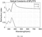
- the electron transport layer comprises BPyTP2.
- the anode comprises a metal anode.
- the thickness of the charge generation layer is tuned to match the first and second emission layers with the anti-nodes of a metal-metal cavity defined by the metal anode and metal cathode.
- the first and second emission layers are configured to emit blue light.
- the first and second emission layers each have a thickness of 60 nm to 70 nm.
- the first emission layer or second emission layer comprises a first layer with a thickness of 5 nm comprising SiCzCz, a second layer with a thickness of 5nm comprising mSiTrz, and a third layer between the first and second layers with a thickness of 50 nm to 60 nm comprising SiCzCz:SiTrzCz2 (1:1) and PtON-TBBI doped 6-13 vol%.
- the first emission layer or second emission layer comprises a first layer with a thickness of 55 nm to 65 nm comprising mCBP:Ir(dmp) 3 doped 18-8 vol%, and a second layer above or below the first layer with a thickness of 5 nm comprising mCBP.
- the charge generation layer has a thickness of 30 nm to 100 nm.
- the charge generation layer comprises a first layer with a thickness of 8 nm to 30 nm comprising BPyTP2, a second layer with a thickness of 15 nm to 40 nm comprising a composition of BCFN and HATCN, and a third layer between the first and second layers with a thickness of 12 nm comprising BPyTP2:Li 2%.
- the anode comprises an Ag composite electrode.
- the Ag composite electrode comprises a first layer of thickness 20 nm to 70 nm comprising ITO, a second layer above the first layer with a thickness of 2 nm to 3 nm comprising Ti or NiCr, a third layer above the second layer with a thickness of 15 nm to 20 nm comprising Ag, a fourth layer above the third layer with a thickness of 2 nm to 3 nm comprising Al, Ti, TiO 2 , or NiCr, and a fifth layer above the fourth layer with a thickness of 5 nm to 20 nm comprising ITO.
- the substrate comprises glass.
- the device has a lifetime enhancement of at least 36 times.
- a product comprises the device as described above, where the product is selected from the group consisting of a flat panel display, a curved display, a computer monitor, a computer, a medical monitor, a television, a billboard, a light for interior or exterior illumination and/or signaling, a heads-up display, a fully or partially transparent display, a flexible display, a rollable display, a foldable display, a stretchable display, a laser printer, a telephone, a mobile phone, a tablet, a phablet, a personal digital assistant (PDA), a wearable device, a laptop computer, a digital camera, a camcorder, a viewfinder, a micro-display, a 3-D display, a virtual reality or augmented reality display or device, a vehicle, a video wall comprising multiple displays tiled together, a theater or stadium screen, a light therapy device, a camera, an imaging device, and a sign.
- PDA personal digital assistant
- an organic light emitting device comprises a substrate, a reflector above the substrate, a first electrode above the reflector, an emissive layer above the first electrode, an electron transport layer above the emissive layer, and a second electrode above the electron transport layer wherein the electron transport layer and the second electrode are configured to form plasmon exciton polaritons between the second electrode and the electron transport layer.
- the device further comprises at least one of a hole blocking layer, electron blocking layer, a hole transport layer, and a hole injection layer between the first electrode and the emissive layer.
- the device further comprises a second hole blocking layer between the emissive layer and the electron transport layer.
- the device further comprises a buffer layer between the electron transport layer and the second electrode.
- the reflector comprises a distributed Bragg reflector.
- the OLED includes a cavity between the first and second electrodes.
- the emissive layer is positioned to span an antinode of the cavity.
- the second electrode comprises a metal electrode.
- the emissive layer comprises a blue emissive layer.
- the emissive layer comprises a phosphorescent emitter material.
- the phosphorescent emitter material is a blue phosphorescent emitter material.
- the emissive layer comprises a sensitizer material and an acceptor material and wherein the sensitizer material transfers energy to the acceptor material.
- the acceptor material is a fluorescent emitter material.
- the sensitizer material is selected from the group consisting of a phosphorescent material or delayed fluorescent material.
- the sensitizer material is a blue emissive material.
- the fluorescent emitter material can be a delayed fluorescent emitter material.
- the electron transport layer has a large oscillator strength at wavelengths shorter than a triplet emission wavelength of the organic emissive layer.
- the reflector has a reflectivity in a range of 50-100%.
- the reflector has a reflectivity of 50-80%.
- the reflector has a reflectivity of 60-70%.
- an organic light emitting device comprises a substrate, a first electrode above the substrate, an emitter stack above the first electrode, comprising a charge generation layer between first and second emission layers, and a second electrode above the emitter stack.
- the device further comprises at least one of a hole transport layer and hole injection layer between the first electrode and the emitter stack, with an absorption tail that overlaps at least a first portion of a first emission spectrum of a first triplet controlled emitting material of the emitter stack.
- the at least one of the hole transport layer and hole injection layer has a thickness of 1 nm to 40 nm, or about 10 nm, or combined thickness of 5 nm to 40 nm.
- the at least one of the hole transport layer and hole injection layer comprises a composition of BCFN and HATCN.
- the device further comprises a electron transport layer between the emitter stack and the second electrode, with an absorption tail that overlaps at least a second portion of a second emission spectrum of a second triplet controlled emitting material of the emitter stack.
- the first and second triplet controlled emitting materials of the emitter stack may be the same or different.
- the first and second emission spectrums may be the same or different.
- the first and second portions of the emission spectrums may be the same or different.
- the electron transport layer has a thickness of 5 nm to 60 nm.
- the electron transport layer comprises BPyTP2.
- the first and second electrodes comprise metal electrodes.
- the thickness of the charge generation layer is tuned to match the first and second emission layers with the anti-nodes of a metal-metal cavity defined by the first and second electrodes.
- the first and second emission layers are configured to emit blue light.
- the first and second emission layers each have a thickness of 60 nm to 70 nm.
- the first emission layer or second emission layer comprises a first layer with a thickness of 5 nm comprising SiCzCz, a second layer with a thickness of 5nm comprising mSiTrz, and a third layer between the first and second layers with a thickness of 50 nm to 60 nm comprising SiCzCz:SiTrzCz2 (1:1) and PtON-TBBI doped 6-13 vol%.
- the first emission layer or second emission layer comprises a first layer with a thickness of 55 nm to 65 nm comprising mCBP:Ir(dmp) 3 doped 18-8 vol%, and a second layer above or below the first layer with a thickness of 5 nm comprising mCBP.
- the charge generation layer has a thickness of 30 nm to 100 nm.
- the charge generation layer comprises a first layer with a thickness of 8 nm to 30 nm comprising BPyTP2, a second layer with a thickness of 15 nm to 40 nm comprising a composition of BCFN and HATCN, and a third layer between the first and second layers with a thickness of 12 nm comprising BPyTP2:Li 2%.
- the first electrode comprises an Ag composite electrode.
- the Ag composite electrode comprises a first layer of thickness 20 nm to 70 nm comprising ITO, a second layer above the first layer with a thickness of 2 nm to 3 nm comprising Ti or NiCr, a third layer above the second layer with a thickness of 15 nm to 20 nm comprising Ag, a fourth layer above the third layer with a thickness of 2 nm to 3 nm comprising Al, Ti, TiO 2 , or NiCr, and a fifth layer above the fourth layer with a thickness of 5 nm to 20 nm comprising ITO.
- the substrate comprises glass.
- the device has a lifetime enhancement of at least 36 times.
- a product comprises the device as described above, where the product is selected from the group consisting of a flat panel display, a curved display, a computer monitor, a computer, a medical monitor, a television, a billboard, a light for interior or exterior illumination and/or signaling, a heads-up display, a fully or partially transparent display, a flexible display, a rollable display, a foldable display, a stretchable display, a laser printer, a telephone, a mobile phone, a tablet, a phablet, a personal digital assistant (PDA), a wearable device, a laptop computer, a digital camera, a camcorder, a viewfinder, a micro-display, a 3-D display, a virtual reality or augmented reality display or device, a vehicle, a video wall comprising multiple displays tiled together, a theater or stadium screen, a light therapy device, a camera, an imaging device, and a sign.
- PDA personal digital assistant
- an organic light emitting device comprises a substrate, a first electrode above the substrate, two or more emitter stacks above the first electrode, each stack comprising alternating emission layers and charge generation layers, with emission layers as the top most and bottom most layers, a second electrode above the emitter stack, a hole transport layer or hole injection layer between the first electrode and the emitter stacks with an absorption tail that overlaps at least a first portion of a first emission spectrum of a first triplet controlled emitting material of the emitter stacks, and an electron transport layer between the emitter stack and the second electrode with an absorption tail that overlaps at least a second portion of a second emission spectrum of a second triplet controlled emitting material of the emitter stacks.
- a stacked organic light emitting device comprises a substrate, a first electrode above the substrate, a second electrode above the first electrode, and two or more emission layers employing polariton-enhanced Purcell effects in the regions of the first and second electrodes.
- an organic light emitting device comprises an anode, an organic emissive layer positioned over the anode, the organic emissive layer comprising a host material and a dopant, an electron transport layer positioned over the organic emissive layer, having a thickness of less than 20 nm and an absorption tail that overlaps a portion of the emission spectrum of the emissive layer, and a metal cathode positioned over the charge transport layer, wherein the electron transport layer and the cathode are configured to form plasmon exciton polaritons between the metal cathode and the electron transport layer.
- an element means one element or more than one element.
- range format is merely for convenience and brevity and should not be construed as an inflexible limitation on the scope of the invention. Accordingly, the description of a range should be considered to have specifically disclosed all the possible subranges as well as individual numerical values within that range. For example, description of a range such as from 1 to 6 should be considered to have specifically disclosed subranges such as from 1 to 3, from 1 to 4, from 1 to 5, from 2 to 4, from 2 to 6, from 3 to 6 etc., as well as individual numbers within that range, for example, 1, 2, 2.7, 3, 4, 5, 5.3, 6 and any whole and partial increments therebetween. This applies regardless of the breadth of the range.
- software executing the instructions provided herein may be stored on a non-transitory computer-readable medium, wherein the software performs some or all of the steps of the present invention when executed on a processor.
- OLEDs make use of thin organic films that emit light when voltage is applied across the device. OLEDs are becoming an increasingly interesting technology for use in applications such as flat panel displays, illumination, and backlighting. Several OLED materials and configurations are described in U.S. Pat. Nos. 5,844,363 , 6,303,238 , and 5,707,745 , which are incorporated herein by reference in their entirety.
- One application for phosphorescent emissive molecules is a full color display. Industry standards for such a display call for pixels adapted to emit particular colors, referred to as "saturated" colors. In particular, these standards call for saturated red, green, and blue pixels. Color may be measured using CIE coordinates, which are well known to the art.
- a green emissive molecule is tris(2-phenylpyridine) iridium, denoted Ir(ppy) 3 , which has the following structure:
- organic includes polymeric materials as well as small molecule organic materials that may be used to fabricate organic opto-electronic devices.
- Small molecule refers to any organic material that is not a polymer, and "small molecules” may actually be quite large. Small molecules may include repeat units in some circumstances. For example, using a long chain alkyl group as a substituent does not remove a molecule from the "small molecule” class. Small molecules may also be incorporated into polymers, for example as a pendent group on a polymer backbone or as a part of the backbone. Small molecules may also serve as the core moiety of a dendrimer, which consists of a series of chemical shells built on the core moiety.
- the core moiety of a dendrimer may be a fluorescent or phosphorescent small molecule emitter.
- a dendrimer may be a "small molecule,” and it is believed that all dendrimers currently used in the field of OLEDs are small molecules.
- top means furthest away from the substrate, while “bottom” means closest to the substrate.
- first layer is described as “disposed over” a second layer, the first layer is disposed further away from substrate. There may be other layers between the first and second layer, unless it is specified that the first layer is "in contact with” the second layer.
- a cathode may be described as “disposed over” an anode, even though there are various organic layers in between.
- solution processible means capable of being dissolved, dispersed, or transported in and/or deposited from a liquid medium, either in solution or suspension form.
- a ligand may be referred to as "photoactive” when it is believed that the ligand directly contributes to the photoactive properties of an emissive material.
- a ligand may be referred to as "ancillary” when it is believed that the ligand does not contribute to the photoactive properties of an emissive material, although an ancillary ligand may alter the properties of a photoactive ligand.
- a first "Highest Occupied Molecular Orbital” (HOMO) or “Lowest Unoccupied Molecular Orbital” (LUMO) energy level is “greater than” or "higher than” a second HOMO or LUMO energy level if the first energy level is closer to the vacuum energy level.
- IP ionization potentials
- a higher HOMO energy level corresponds to an IP having a smaller absolute value (an IP that is less negative).
- a higher LUMO energy level corresponds to an electron affinity (EA) having a smaller absolute value (an EA that is less negative).
- the LUMO energy level of a material is higher than the HOMO energy level of the same material.
- a "higher” HOMO or LUMO energy level appears closer to the top of such a diagram than a "lower” HOMO or LUMO energy level.
- a first work function is "greater than” or “higher than” a second work function if the first work function has a higher absolute value. Because work functions are generally measured as negative numbers relative to vacuum level, this means that a "higher” work function is more negative. On a conventional energy level diagram, with the vacuum level at the top, a “higher” work function is illustrated as further away from the vacuum level in the downward direction. Thus, the definitions of HOMO and LUMO energy levels follow a different convention than work functions.
- the initial OLEDs used emissive molecules that emitted light from their singlet states ("fluorescence") as disclosed, for example, in U.S. Pat. No. 4,769,292 , which is incorporated by reference in its entirety. Fluorescent emission generally occurs in a time frame of less than 10 nanoseconds.
- FIG. 1 shows an organic light emitting device 100.
- Device 100 may include a substrate 110, an anode 115, a hole injection layer 120, a hole transport layer 125, an electron blocking layer 130, an emissive layer 135, a hole blocking layer 140, an electron transport layer 145, an electron injection layer 150, a protective layer 155, a cathode 160, and a barrier layer 170.
- Cathode 160 is a compound cathode having a first conductive layer 162 and a second conductive layer 164.
- Device 100 may be fabricated by depositing the layers described, in order. The properties and functions of these various layers, as well as example materials, are described in more detail in US 7,279,704 at cols. 6-10, which are incorporated by reference.
- each of these layers are available.
- a flexible and transparent substrate-anode combination is disclosed in U.S. Pat. No. 5,844,363 , which is incorporated by reference in its entirety.
- An example of a p-doped hole transport layer is m-MTDATA doped with F 4 -TCNQ at a molar ratio of 50:1, as disclosed in U.S. Patent Application Publication No. 2003/0230980 , which is incorporated by reference in its entirety.
- Examples of emissive and host materials are disclosed in U.S. Pat. No. 6,303,238 to Thompson et al. , which is incorporated by reference in its entirety.
- An example of an n-doped electron transport layer is BPhen doped with Li at a molar ratio of 1:1, as disclosed in U.S. Patent Application Publication No. 2003/0230980 , which is incorporated by reference in its entirety.
- U.S. Pat. Nos. 5,703,436 and 5,707,745 which are incorporated by reference in their entireties, disclose examples of cathodes including compound cathodes having a thin layer of metal such as Mg:Ag with an overlying transparent, electrically-conductive, sputter-deposited ITO layer.
- the theory and use of blocking layers is described in more detail in U.S. Pat. No. 6,097,147 and U.S. Patent Application Publication No.
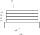
- FIG. 2 shows an inverted OLED 200.
- the device includes a substrate 210, a cathode 215, an emissive layer 220, a hole transport layer 225, and an anode 230.
- Device 200 may be fabricated by depositing the layers described, in order. Because the most common OLED configuration has a cathode disposed over the anode, and device 200 has cathode 215 disposed under anode 230, device 200 may be referred to as an "inverted" OLED. Materials similar to those described with respect to device 100 may be used in the corresponding layers of device 200.
- FIG. 2 provides one example of how some layers may be omitted from the structure of device 100.
- FIGS. 1 and 2 The simple layered structure illustrated in FIGS. 1 and 2 is provided by way of non-limiting example, and it is understood that embodiments of the disclosure may be used in connection with a wide variety of other structures.
- the specific materials and structures described are exemplary in nature, and other materials and structures may be used.
- Functional OLEDs may be achieved by combining the various layers described in different ways, or layers may be omitted entirely, based on design, performance, and cost factors. Other layers not specifically described may also be included. Materials other than those specifically described may be used. Although many of the examples provided herein describe various layers as comprising a single material, it is understood that combinations of materials, such as a mixture of host and dopant, or more generally a mixture, may be used. Also, the layers may have various sublayers.
- hole transport layer 225 transports holes and injects holes into emissive layer 220, and may be described as a hole transport layer or a hole injection layer.
- an OLED may be described as having an "organic layer" disposed between a cathode and an anode. This organic layer may comprise a single layer, or may further comprise multiple layers of different organic materials as described, for example, with respect to FIGS. 1 and 2 .
- OLEDs comprised of polymeric materials (PLEDs) such as disclosed in U.S. Pat. No. 5,247,190 to Friend et al. , which is incorporated by reference in its entirety.
- PLEDs polymeric materials
- OLEDs having a single organic layer may be used.
- OLEDs may be stacked, for example as described in U.S. Pat. No. 5,707,745 to Forrest et al , which is incorporated by reference in its entirety.
- the OLED structure may deviate from the simple layered structure illustrated in FIGS. 1 and 2 .
- the substrate may include an angled reflective surface to improve out-coupling, such as a mesa structure as described in U.S. Pat. No. 6,091,195 to Forrest et al. , and/or a pit structure as described in U.S. Pat. No. 5,834,893 to Bulovic et al. , which are incorporated by reference in their entireties.
- any of the layers of the various embodiments may be deposited by any suitable method.
- preferred methods include thermal evaporation, ink-jet, such as described in U.S. Pat. Nos. 6,013,982 and 6,087,196 , which are incorporated by reference in their entireties, organic vapor phase deposition (OVPD), such as described in U.S. Pat. No. 6,337,102 to Forrest et al. , which is incorporated by reference in its entirety, and deposition by organic vapor jet printing (OVJP), such as described in U.S. Pat. No. 7,431,968 , which is incorporated by reference in its entirety.
- OVPD organic vapor phase deposition
- OJP organic vapor jet printing
- Other suitable deposition methods include spin coating and other solution based processes.
- Solution based processes are preferably carried out in nitrogen or an inert atmosphere.
- preferred methods include thermal evaporation.
- Preferred patterning methods include deposition through a mask, cold welding such as described in U.S. Pat. Nos. 6,294,398 and 6,468,819 , which are incorporated by reference in their entireties, and patterning associated with some of the deposition methods such as ink-jet and OVJD. Other methods may also be used.
- the materials to be deposited may be modified to make them compatible with a particular deposition method. For example, substituents such as alkyl and aryl groups, branched or unbranched, and preferably containing at least 3 carbons, may be used in small molecules to enhance their ability to undergo solution processing.
- Substituents having 20 carbons or more may be used, and 3-20 carbons is a preferred range. Materials with asymmetric structures may have better solution processibility than those having symmetric structures, because asymmetric materials may have a lower tendency to recrystallize. Dendrimer substituents may be used to enhance the ability of small molecules to undergo solution processing.
- Devices fabricated in accordance with embodiments of the present disclosure may further optionally comprise a barrier layer.
- a barrier layer One purpose of the barrier layer is to protect the electrodes and organic layers from damaging exposure to harmful species in the environment including moisture, vapor and/or gases, etc.
- the barrier layer may be deposited over, under or next to a substrate, an electrode, or over any other parts of a device including an edge.
- the barrier layer may comprise a single layer, or multiple layers.
- the barrier layer may be formed by various known chemical vapor deposition techniques and may include compositions having a single phase as well as compositions having multiple phases. Any suitable material or combination of materials may be used for the barrier layer.
- the barrier layer may incorporate an inorganic or an organic compound or both.
- the preferred barrier layer comprises a mixture of a polymeric material and a non-polymeric material as described in U.S. Pat. No. 7,968,146 , PCT Pat. Application Nos. PCT/US2007/023098 and PCT/US2009/042829 , which are herein incorporated by reference in their entireties.
- the aforesaid polymeric and non-polymeric materials comprising the barrier layer should be deposited under the same reaction conditions and/or at the same time.
- the weight ratio of polymeric to non-polymeric material may be in the range of 95:5 to 5:95.
- the polymeric material and the non-polymeric material may be created from the same precursor material.
- the mixture of a polymeric material and a non-polymeric material consists essentially of polymeric silicon and inorganic silicon.
- Devices fabricated in accordance with embodiments of the disclosure can be incorporated into a wide variety of electronic component modules (or units) that can be incorporated into a variety of electronic products or intermediate components. Examples of such electronic products or intermediate components include display screens, lighting devices such as discrete light source devices or lighting panels, etc. that can be utilized by the end-user product manufacturers. Such electronic component modules can optionally include the driving electronics and/or power source(s). Devices fabricated in accordance with embodiments of the disclosure can be incorporated into a wide variety of consumer products that have one or more of the electronic component modules (or units) incorporated therein.
- a consumer product comprising an OLED that includes the compound of the present disclosure in the organic layer in the OLED is disclosed.
- Such consumer products would include any kind of products that include one or more light source(s) and/or one or more of some type of visual displays.
- Some examples of such consumer products include flat panel displays, curved displays, computer monitors, medical monitors, televisions, billboards, lights for interior or exterior illumination and/or signaling, heads-up displays, fully or partially transparent displays, flexible displays, rollable displays, foldable displays, stretchable displays, laser printers, telephones, mobile phones, tablets, phablets, personal digital assistants (PDAs), wearable devices, laptop computers, digital cameras, camcorders, viewfinders, micro-displays (displays that are less than 2 inches diagonal), 3-D displays, virtual reality or augmented reality displays, vehicles, video walls comprising multiple displays tiled together, theaters or stadium screens, light therapy devices, and signs.
- control mechanisms may be used to control devices fabricated in accordance with the present disclosure, including passive matrix and active matrix. Many of the devices are intended for use in a temperature range comfortable to humans, such as 18 C to 30 C, and more preferably at room temperature (20-25 C), but could be used outside this temperature range, for example, from -40 C to 80 C.
- the OLED has one or more characteristics selected from the group consisting of being flexible, being rollable, being foldable, being stretchable, and being curved. In some embodiments, the OLED is transparent or semi-transparent. In some embodiments, the OLED further comprises a layer comprising carbon nanotubes.
- the enhancement layer comprises a plasmonic material exhibiting surface plasmon resonance that non-radiatively couples to the emitter material and transfers excited state energy from the emitter material to non-radiative mode of surface plasmon polariton.
- the enhancement layer is provided no more than a threshold distance away from the organic emissive layer, wherein the emitter material has a total non-radiative decay rate constant and a total radiative decay rate constant due to the presence of the enhancement layer and the threshold distance is where the total non-radiative decay rate constant is equal to the total radiative decay rate constant.
- the OLED further comprises an outcoupling layer.
- the outcoupling layer is disposed over the enhancement layer on the opposite side of the organic emissive layer.
- the outcoupling layer is disposed on opposite side of the emissive layer from the enhancement layer but still outcouples energy from the surface plasmon mode of the enhancement layer.
- the outcoupling layer scatters the energy from the surface plasmon polaritons. In some embodiments this energy is scattered as photons to free space. In other embodiments, the energy is scattered from the surface plasmon mode into other modes of the device such as but not limited to the organic waveguide mode, the substrate mode, or another waveguiding mode.
- one or more intervening layers can be disposed between the enhancement layer and the outcoupling layer.
- the examples for intervening layer(s) can be dielectric materials, including organic, inorganic, perovskites, oxides, and may include stacks and/or mixtures of these materials.
- the enhancement layer modifies the effective properties of the medium in which the emitter material resides resulting in any or all of the following: a decreased rate of emission, a modification of emission line-shape, a change in emission intensity with angle, a change in the stability of the emitter material, a change in the efficiency of the OLED, and reduced efficiency roll-off of the OLED device. Placement of the enhancement layer on the cathode side, anode side, or on both sides results in OLED devices which take advantage of any of the above-mentioned effects.
- the OLEDs according to the present disclosure may include any of the other functional layers often found in OLEDs.
- the enhancement layer can be comprised of plasmonic materials, optically active metamaterials, or hyperbolic metamaterials.
- a plasmonic material is a material in which the real part of the dielectric constant crosses zero in the visible or ultraviolet region of the electromagnetic spectrum.
- the plasmonic material includes at least one metal.
- the metal may include at least one of Ag, Al, Au, Ir, Pt, Ni, Cu, W, Ta, Fe, Cr, Mg, Ga, Rh, Ti, Ru, Pd, In, Bi, Ca alloys or mixtures of these materials, and stacks of these materials.
- a metamaterial is a medium composed of different materials where the medium as a whole acts differently than the sum of its material parts.
- optically active metamaterials as materials which have both negative permittivity and negative permeability.
- Hyperbolic metamaterials are anisotropic media in which the permittivity or permeability are of different sign for different spatial directions.
- Optically active metamaterials and hyperbolic metamaterials are strictly distinguished from many other photonic structures such as Distributed Bragg Reflectors ("DBRs") in that the medium should appear uniform in the direction of propagation on the length scale of the wavelength of light.
- DBRs Distributed Bragg Reflectors
- the dielectric constant of the metamaterials in the direction of propagation can be described with the effective medium approximation. Plasmonic materials and metamaterials provide methods for controlling the propagation of light that can enhance OLED performance in a number of ways.
- the enhancement layer is provided as a planar layer.
- the enhancement layer has wavelength-sized features that are arranged periodically, quasi-periodically, or randomly, or sub-wavelength-sized features that are arranged periodically, quasi-periodically, or randomly.
- the wavelength-sized features and the sub-wavelength-sized features have sharp edges.
- the outcoupling layer has wavelength-sized features that are arranged periodically, quasi-periodically, or randomly, or sub-wavelength-sized features that are arranged periodically, quasi-periodically, or randomly.
- the outcoupling layer may be composed of a plurality of nanoparticles and in other embodiments the outcoupling layer is composed of a plurality of nanoparticles disposed over a material.
- the outcoupling may be tunable by at least one of varying a size of the plurality of nanoparticles, varying a shape of the plurality of nanoparticles, changing a material of the plurality of nanoparticles, adjusting a thickness of the material, changing the refractive index of the material or an additional layer disposed on the plurality of nanoparticles, varying a thickness of the enhancement layer, and/or varying the material of the enhancement layer.
- the plurality of nanoparticles of the device may be formed from at least one of metal, dielectric material, semiconductor materials, an alloy of metal, a mixture of dielectric materials, a stack or layering of one or more materials, and/or a core of one type of material and that is coated with a shell of a different type of material.
- the outcoupling layer is composed of at least metal nanoparticles wherein the metal is selected from the group consisting of Ag, Al, Au, Ir, Pt, Ni, Cu, W, Ta, Fe, Cr, Mg, Ga, Rh, Ti, Ru, Pd, In, Bi, Ca, alloys or mixtures of these materials, and stacks of these materials.
- the plurality of nanoparticles may have additional layer disposed over them.
- the polarization of the emission can be tuned using the outcoupling layer. Varying the dimensionality and periodicity of the outcoupling layer can select a type of polarization that is preferentially outcoupled to air. In some embodiments the outcoupling layer also acts as an electrode of the device.
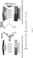
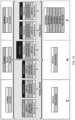
- PEPs are a strongly coupled state at the metal/dielectric interface resulting from mixing of the SPP mode of the metal with excitons in the adjacent dielectric layer(s).
- EML PHOLED emission layer
- PEP strength is a function of the oscillator strengths of both the cathode and electron transport layer (ETL), see Fig. 3 (right).
- the light extraction efficiency and the emission color saturation are increased.
- a portion of the ETL absorption spectrum such as the long wavelength tail (i.e. imaginary part of index of refraction) is in the emission spectrum of the EML.
- the polariton is detuned from absorption.
- the ETL absorption spectrum (or the imaginary part of index of refraction) is higher than (i.e. shorter wavelength) the emission spectrum of the EML, instead in the EML emission spectrum.
- the polariton is detuned to overlap with the EML emission to enhance the Purcell effect, instead of detuning from the absorption. In some embodiments, this overlap can be tuned to balance light extraction and absorption. In some embodiments, inefficient triplets are encouraged to radiate into polaritons.
- the Commission Internationale d'Eclairage (CIE) coordinates of the conventional Ir(dmp) 3 PHOLED shift from cyan at (0.16, 0.26), to deep blue at (0.14, 0.14), gaining almost three-fold increase in LT90 using the Purcell effect enhanced by the strong Ag SPP, while maintaining the same EQE.
- CIE Commission Internationale d'Eclairage
- a strongly coupled PEP state is formed at the metal cathode/ETL interface at wavelengths where the ETL singlet exciton is resonant with the SPP mode of the cathode, see Fig. 8 for chemical structures of the molecules used.
- resonance is defined by the ETL singlet exciton absorption peak (i.e. major frequency).
- the SPP mode is broad spectrum, and one or a few wavelengths are chosen out of that spectrum.
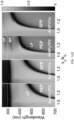
- Fig. 4 shows the match between the measured and calculated angle-resolved spectra, respectively.
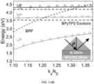
- the strongly coupled PEPs for the AI/BPyTP2 combination dispersion splits into upper (UP), middle (MP) and lower polariton (LP) branches.
- the overlap between the AI/BPyTP2 LP energy and the Ir(dmp) 3 triplet emission is, therefore, larger than the AI/SF3Trz polariton.
- the splitting between the BPyTP2 exciton and the Ag/BPyTP2 PEP dispersion is even larger owing to the stronger SPP in Ag than Al.
- the MP and UP branches are not observed due to their higher energy than the Ag absorption band.
- the Ag/BPyTP2 PEP has an asymptotically flat region limited by the BPyTP2 exciton energy at 1 ⁇ k x /k 0 ⁇ ⁇ .
- k 0 is the wavevector in vacuum. Therefore, Ag/BPyTP2 shows the most complete overlap between the PEP and the blue-cyan region at wavelengths of 400-500 nm, followed by Ag/SF3Trz > AI/BPyTP2 > AI/SF3Trz.
- Fig. 4 also shows the angular photoluminescence (PL).
- the Ag/BPyTP2 PEP LP branch shows a PL intensity that is two orders of magnitude higher than the other three cathode/ETLs, showing enhanced mixing between the SPP and ETL excitons. Note that the strong coupling is between the ETL and the cathode, and the triplet from the blue phosphor emission is transferred to the PEPs in the weak coupling regime due to the low oscillator strength of triplets.
- Fig. 5A illustrates several exemplary PHOLED structures labeled as C, H and F (see. Fig. 10 for further devices studied).
- an organic light emitting device 300 comprises an anode 303, an organic emissive layer 305 positioned over the anode 303, the organic emissive layer 305 comprising a host material and a dopant, a charge transport layer 307 positioned over the organic emissive layer 305, having a thickness of less than 20 nm, and a metal cathode 309 positioned over the charge transport layer 307, wherein the charge transport layer 307 and the cathode 309 are configured to form plasmon exciton polaritons between the metal cathode 309 and the charge transport layer 307.
- the device 300 further comprises a reflector 302 positioned under the anode.
- the reflector 302 comprises a stack of layers of alternating materials.
- the reflector 302 and the cathode 309 form a cavity having a total cavity Q of 5 or less, a total cavity Q of 4 or less, a total cavity Q of 3 or less, or any other suitable Q.
- at least a portion of the organic emissive layer 305 is at an antinode of the cavity.
- the metal cathode 309 is selected from the group consisting of Ag, Au, Ag alloys, and/or Au alloys.
- the charge transport layer 307 has a thickness less than 18 nm, less than 15 nm, less than 10 nm, or any other suitable thickness. In some embodiments, the charge transport layer 307 comprises an electron transport layer 307.
- the device 300 further comprises a blocking layer and/or buffer layer 308 between the metal cathode 309 and the charge transport layer 307.
- the blocking layer and/or buffer layer 308 prevents diffusion between the metal cathode 309 and the charge transport layer 307.
- the blocking layer and/or buffer layer 308 is two or more layers.
- at least one layer of the two or more layers is made of Al.
- the at least one layer is adjacent to the metal cathode 309.
- the at least one layer is less than 3 nm thick.
- at least one layer of the two or more layers is Liq (8-Hydroxyquinolinolato-lithium).
- the at least one layer is adjacent to the electron transport layer 307.
- an interface is formed between the metal cathode 309 and the charge transport layer 307.
- plasmon exciton polariton strength is a function of the oscillator strength of the metal cathode 309 and the electron transport layer 307.
- a consumer product comprises the device 300 as described above, wherein the consumer product is selected from the group consisting of a flat panel display, a curved display, a computer monitor, a medical monitor, a television, a billboard, a light for interior or exterior illumination and/or signaling, a heads-up display, a fully or partially transparent display, a flexible display, a rollable display, a foldable display, a stretchable display, a laser printer, a telephone, a cell phone, tablet, a phablet, a personal digital assistant (PDA), a wearable device, a laptop computer, a digital camera, a camcorder, a viewfinder, a micro-display that is less than 2 inches diagonal, a 3-D display, a virtual reality or augmented reality display, a vehicle, a video walls comprising multiple displays tiled together, a theater or stadium screen, a light therapy device, and a sign.
- PDA personal digital assistant
- an organic light emitting device (OLED) 300 comprises a substrate 301, a reflector 302 above the substrate 301, a first electrode 303 above the reflector 302, an emissive layer 305 above the first electrode 303, an electron transport layer 307 above the emissive layer 305, and a second electrode 309 above the electron transport layer 307 wherein the electron transport layer 307 and the second electrode 309 are configured to form plasmon exciton polaritons between the second electrode 309 and the electron transport layer 307.
- the device 300 further comprises at least one of a hole blocking layer, electron blocking layer, a hole transport layer, and a hole injection layer (collectively 304) between the first electrode 303 and the emissive layer 305.
- the device 300 further comprises a second hole blocking layer 306 between the emissive layer 305 and the electron transport layer 307.
- the device 300 further comprises a buffer layer 308 between the electron transport layer 307 and the second electrode 309.
- the reflector 302 comprises a distributed Bragg reflector. In some embodiments, the reflector 302 has a reflectivity in a range of 50-100%, 50-80%, 60-70%, or any other suitable range.
- the OLED 300 includes a cavity between the first electrode 301 and second electrode 309.
- the emissive layer 305 is positioned to span an antinode of the cavity.
- the second electrode 309 comprises a metal electrode.
- the emissive layer 305 comprises a blue, green, red, white, infrared, ultraviolet, and/or broad-spectrum emissive layer and/or emissive layer stack comprising a combination of a blue, green, red, white, infrared, ultraviolet, and/or broad-spectrum emissive layers.
- the emissive layer 305 comprises a phosphorescent emitter material.
- the phosphorescent emitter material is a blue phosphorescent emitter material.
- the emissive layer 305 comprises a sensitizer material and an acceptor material and wherein the sensitizer material transfers energy to the acceptor material.
- the acceptor material is a fluorescent emitter material.
- the sensitizer material is selected from the group consisting of a phosphorescent material or delayed fluorescent material.
- the sensitizer material is a blue emissive material.
- the fluorescent emitter material can be a delayed fluorescent emitter material.
- the electron transport layer 307 has a large oscillator strength at wavelengths shorter than a triplet emission wavelength of the organic emissive layer. In some embodiments, the electron transport layer 307 has a large oscillator strength at wavelengths 0.1 nm to 1000 nm, 1 nm to 100 nm, 1 nm to 50 nm, 1 nm to 20 nm, 0.1 nm to 15 nm, 0.1 nm to 5 nm, about 1 nm, about 2 nm, about 5 nm, about 10 nm, about 15 nm, about 20 nm, less than 25 nm, or other suitable wavelength shorter than the triplet emission wavelength of the organic emissive layer.
- the half cavity device H compared to device C with a conventional Al cathode and an ITO anode, the half cavity device H employs an Ag cathode buffered by a 3 nm thick Al layer supporting enhanced energy transfer to polariton modes.
- full cavity device F is identical to H except that it employs a bottom Distributed Bragg Reflector (DBR) and the top Ag cathode low-Q cavity used to tune the emission color.
- DBR Distributed Bragg Reflector
- low-Q cavities are created by utilizing mirrors or DBRs that aren't as reflective due to fewer mirror/reflector layers and/or material choice.
- the DBR has a reflectivity of about 50%-100%, about 50%-80%, or about 60%-70%.
- the calculated distribution of radiative and nonradiative channels at 465-475nm in the three archetype exemplary Ir(dmp) 3 devices is illustrated in the histograms of Fig. 5A , while the optical density of states (ODoS) distributions are shown in Fig. 11A .
- the ODoS and the PF are increased via enhanced polariton energy transfer near the Ag/BPyTP2 or Ag/SF3Trz in devices H and F.
- the Al buffer layer is used to keep the Ag cathode from diffusing into the ETL.
- cathode can be used which have a strong plasmonic resonance, such as Au and/or Au for red and infrared OLEDs, Al for UV OLEDs, Ag for visible spectrum OLEDS, and/or Au/Ag alloys such as MgAg.
- Other materials for the barrier can be used that are transparent to the emission such as organics with a wide band gap energy, polyaromatic hydrocarbons (PAH), and/or oxidative metals such as Cr, Ti, and Ni.
- PAH polyaromatic hydrocarbons
- oxidative metals such as Cr, Ti, and Ni.
- the generation of defects by TPA/TTA is reduced via reducing the triplet density by increasing the radiative rate, which is directly proportional to PF.
- the defect generation rate is consequently slowed in devices H and F, indicated by the shorter red arrows in Fig. 5A .
- ⁇ PL a larger defect density is required in devices H and F to match the increased radiative energy transfer, indicated by the larger dashed rectangular area at LT85. This suggests a nonlinear dependence between device lifetime and PF (see Methods).
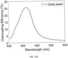
- the Ag/DBR cavity mode in F increases the outcoupling efficiency compared to H, corresponding to k x /k 0 ⁇ 1, by placing the EML at the antinode of the Ag/DBR cavity mode 4 . Consequently, the Ag/DBR cavity device F features a large PF, an enhanced EQE compared to H, and a narrowed emission spectrum.
- the antinode position depends on wavelength of the EML and size of the cavity formed by the DBR 302 and metal cathode 308/309, such as being positioned halfway through the thickness of the cavity. In some embodiments, at least a portion of the EML spans the antinode of the cavity.
- Fig. 5B shows time-resolved PL (TrPL) of a 50nm thick Ir(cb) 3 EML in structures C, H, and F.
- Samples H and F with an Ag cathode have larger k, than those with an Al cathode (C); those with a BPyTP2 ETL have a larger k, than those with SF3Trz, following the trend of the polariton dispersion in Fig. 4 .
- an exemplary stacked device 400 structure includes stacked EMLs (404, 406) separated by a charge generation layer (CGL) 405.
- a hole injection layer (HIL) and/or a hole transporting layer (HTL) 403, an electron transporting layer (ETL) 407 and an electron injection layer (EIL) 408 is adjacent to the metal electrodes for charge injection.
- the EMLs (404, 406) are blue EMLs.
- the blue EML is typically 60-70nm, and connected to the ETL/cathode, HTL/anode and/or the CGL.
- the EMLs (404, 406) can be any combination of blue EMLs, red EMLs, green EMLs, white EMLs, or other suitable color tint EMLs.
- the thickness of the CGL 405 is fine-tuned to match the metal-metal cavity mode antinodes with the EMLs, where at least a portion of each EML spans at least one cavity antinode.
- the number of EML stacks can be more than two. In some embodiments, only the two EML stacks that connect to the metal electrodes have enhanced stability from polariton-enhanced Purcell effect. In some embodiments, only the two EML stacks closest to the metal electrodes have enhanced stability from polariton-enhanced Purcell effect.
- an organic light emitting device 400 comprises a substrate 401, a first electrode 402 above the substrate 401, an emitter stack 409 above the first electrode 402, and a second electrode 408 above the emitter stack 409.
- the emitter stack 409 comprises a charge generation layer 405 between first 404 and second 406 emission layers.
- an organic light emitting device 400 comprises a substrate 401, a first electrode 402 above the substrate 401, two or more emitter stacks 409 above the first electrode 402, and a second electrode 408 above the two or more emitter stacks 409.
- each emitter stack 409 comprises alternating emission layers (404, 406) and charge generation layers 405, with emission layers (404, 406) as the top most and bottom most layers.
- a stacked organic light emitting device 400 comprises a substrate 401, a first electrode 402 above the substrate, a second electrode 408 above the first electrode 402, and two or more emission layers (404, 406) employing polariton-enhanced Purcell effects in the regions of the first and second electrodes (402, 408).
- the device 400 further comprises a hole transport layer 403 and/or a hole injection layer 403 between the first electrode 402 and the emitter stack(s) 409.
- the hole transport layer 403 and/or hole injection layer 403 is configured to have an absorption tail that overlaps at least a portion of the emission spectrum of one or more triplet controlled emitting materials of the emitter stack 409.
- the hole transport layer 403 and/or hole injection layer 403 has a thickness of 1 nm to 40 nm, or about 10 nm, or combined thickness of 5 nm to 40 nm.
- the hole transport layer 403 and/or the hole injection layer 403 comprises BCFN, HATCN, and/or a composition of BCFN and HATCN.
- the device 400 further comprises an electron transport layer 407 between the emitter stack 409 and the second electrode 408.
- the electron transport layer 407 is configured to have an absorption tail that overlaps at least a portion of the emission spectrum of one or more triplet controlled emitting materials of the emitter stack 409.
- the electron transport layer 407 has a thickness of 5 nm to 60 nm.
- the electron transport layer 407 comprises BPyTP2.
- the first and/or second electrodes (402, 408) comprise a metal electrode.
- the thickness of the charge generation layer 405 is tuned to match the anti-modes of a metal-metal cavity defined by the first and second electrodes (402, 408) with the first and second emission layers (404, 406) or emitter stack 409.
- the charge generation layer 405 has a thickness of 30 nm to 100 nm.
- the charge generation layer 405 comprises a first layer with a thickness of 8 nm to 30 nm comprising BPyTP2, a second layer with a thickness of 15 nm to 40 nm comprising a composition of BCFN and HATCN, and a third layer between the first and second layers with a thickness of 12 nm comprising BPyTP2:Li 2%.
- the charge generation layer 405 may be made of any combination of layers comprising either BPyTP2, BCFN, HATCN, or BPyTP2:Li 2%, or any combination thereof including any other materials known in the art.
- the first and/or second emission layers (404, 406) are configured to emit blue light. In some embodiments, the first and/or second emission layers (404, 406) each have a thickness of 60 nm to 70 nm. In some embodiments, the first and/or second emission layers (404, 406) may be configured to emit any color light including blue, red, green and/or white.
- the first emission layer 404 and/or second emission layer 406 comprises a first layer with a thickness of 5 nm comprising SiCzCz, a second layer with a thickness of 5nm comprising mSiTrz, and a third layer between the first and second layers with a thickness of 50 nm to 60 nm comprising SiCzCz:SiTrzCz2 (1:1) and PtON-TBBI doped 6-13 vol%.
- any emissive layer 404/406 may be made of any combination of layers comprising either SiCzCz, mSiTrz, SiCzCz:SiTrzCz2 (1:1), PtON-TBBI doped 6-13 vol%, or any combination thereof including any other materials known in the art.
- the first emission layer 404 and/or second emission layer 406 comprises a first layer with a thickness of 55 nm to 65 nm comprising mCBP:Ir(dmp) 3 doped 18-8 vol%, and a second layer above or below the first layer with a thickness of 5 nm comprising mCBP.
- any emissive layer 404/406 may be made of any combination of layers comprising either mCBP:Ir(dmp) 3 doped 18-8 vol% or mCBP, or any combination therefore including any other materials known in the art.
- the first electrode 402 comprises an Ag composite electrode. In some embodiments, the first electrode 402 comprises an Ag composite electrode including at least one layer of ITO, Ti, NiCr, Ag, Al, TiO 2 , or any other suitable material or combinations thereof.
- the Ag composite electrode comprises a first layer of thickness 20 nm to 70 nm comprising ITO, a second layer above the first layer with a thickness of 2 nm to 3 nm comprising Ti or NiCr, a third layer above the second layer with a thickness of 15 nm to 20 nm comprising Ag, a fourth layer above the third layer with a thickness of 2 nm to 3 nm comprising Al, Ti, TiO 2 , or NiCr, and a fifth layer above the fourth layer with a thickness of 5 nm to 20 nm comprising ITO.
- the substrate 401 comprises glass.
- the second electrode 408 comprises Ag/AI/Liq or any combination thereof and has a thickness of 100 nm.
- the device 400 has a lifetime enhancement of at least 10 times, at least 20 times, or at least 30 times compared to a conventional device.
- the materials described herein as useful for a particular layer in an organic light emitting device may be used in combination with a wide variety of other materials present in the device.
- emissive dopants disclosed herein may be used in conjunction with a wide variety of hosts, transport layers, blocking layers, injection layers, electrodes and other layers that may be present.
- the materials described or referred to below are non-limiting examples of materials that may be useful in combination with the compounds disclosed herein, and one of skill in the art can readily consult the literature to identify other materials that may be useful in combination.
- a charge transport layer can be doped with conductivity dopants to substantially alter its density of charge carriers, which will in turn alter its conductivity.
- the conductivity is increased by generating charge carriers in the matrix material, and depending on the type of dopant, a change in the Fermi level of the semiconductor may also be achieved.
- Hole-transporting layer can be doped by p-type conductivity dopants and n-type conductivity dopants are used in the electron-transporting layer.
- a hole injecting/transporting material to be used in the present disclosure is not particularly limited, and any compound may be used as long as the compound is typically used as a hole injecting/transporting material.
- An electron blocking layer may be used to reduce the number of electrons and/or excitons that leave the emissive layer.
- the presence of such a blocking layer in a device may result in substantially higher efficiencies, and or longer lifetime, as compared to a similar device lacking a blocking layer.
- a blocking layer may be used to confine emission to a desired region of an OLED.
- the EBL material has a higher LUMO (closer to the vacuum level) and/or higher triplet energy than the emitter closest to the EBL interface.
- the EBL material has a higher LUMO (closer to the vacuum level) and or higher triplet energy than one or more of the hosts closest to the EBL interface.
- the compound used in EBL contains the same molecule or the same functional groups used as one of the hosts described below.
- the light emitting layer of the organic EL device of the present disclosure preferably contains at least a metal complex as light emitting material, and may contain a host material using the metal complex as a dopant material.
- the host material are not particularly limited, and any metal complexes or organic compounds may be used as long as the triplet energy of the host is larger than that of the dopant. Any host material may be used with any dopant so long as the triplet criteria is satisfied.
- a hole blocking layer may be used to reduce the number of holes and/or excitons that leave the emissive layer.
- the presence of such a blocking layer in a device may result in substantially higher efficiencies and/or longer lifetime as compared to a similar device lacking a blocking layer.
- a blocking layer may be used to confine emission to a desired region of an OLED.
- the HBL material has a lower HOMO (further from the vacuum level) and or higher triplet energy than the emitter closest to the HBL interface.
- the HBL material has a lower HOMO (further from the vacuum level) and or higher triplet energy than one or more of the hosts closest to the HBL interface.
- An electron transport layer may include a material capable of transporting electrons.
- the electron transport layer may be intrinsic (undoped), or doped. Doping may be used to enhance conductivity. Examples of the ETL material are not particularly limited, and any metal complexes or organic compounds may be used as long as they are typically used to transport electrons.
- the CGL plays an essential role in the performance, which is composed of an n-doped layer and a p-doped layer for injection of electrons and holes, respectively. Electrons and holes are supplied from the CGL and electrodes. The consumed electrons and holes in the CGL are refilled by the electrons and holes injected from the cathode and anode, respectively; then, the bipolar currents reach a steady state gradually.
- Typical CGL materials include n and p conductivity dopants used in the transport layers.
- OLEDs and other similar devices may be fabricated using a variety of techniques and devices. For example, in OVJP and similar techniques, one or more jets of material is directed at a substrate to form the various layers of the OLED.
- Structure 1 employed a 17 nm thick SF3Trz ETL featuring only SPP energy transfer, while 2 and 3 employed 17 nm / 25 nm thick BPyTP2 ETL for PEP energy transfer.
- the product of EQE and the Purcell factor can be used in layer thickness optimization, such that EQE, PF, or their product is optimized based on needed device characteristics.
- the PEP-enhanced F3 with a thicker ETL still features a slightly higher PF than the SPP-enhanced F1 along with a 45% increase in outcoupling efficiency.
- the low-Q Ag/DBR cavity mode has only a small impact on the angular dependence of the emission spectrum, shown in F2 in Fig. 6C .
- the angular dependence of the emission intensity of F2 differs only slightly from C2 (see inset). From C to F, the current-voltage characteristics show no change in devices using the same ETL, see Fig. 12D indicating there is no power penalty associated with this device design.
- Fig. 6D shows the operational lifetime of F1-3 compared to C1-3.
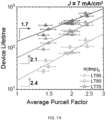
- Aged at a current density of J 7 mA/cm 2 (corresponding to an initial luminance of L 0 ⁇ 1000 cd/m 2 for cyan-emitting C3, see Table 1) a 4.4X enhancement in LT90 is achieved from the most strongly Purcell-enhanced F2 from C2, compared to 2.5X for F1 versus C1 and 2.2X from F3 to C3.
- Fig. 7A summarizes the Ir(dmp) 3 device operational lifetime versus the calculated average PF.
- Fig. 7B summarizes the device performance achieved by the polariton-enhanced Purcell effect, compared to that of the conventional Ir(dmp) 3 device C1 with the lowest PF.
- the enclosed triangular areas are proportional to the total number of equivalent deep blue photons emitted throughout the device lifetime.
- Device F1 achieves the deepest blue color and a 2.7X increase from C1 in lifetime, while maintaining the same EQE as C1.
- Device F2 achieves the longest LT90, a 5.3X increase from C1.
- the EQE is slightly reduced due to the strong, competing energy transfer to PEPs.
- Devices F1-3 reach the best performance along each axis. Therefore, the introduction of PEPs in low-Q cavities significantly increases total deep blue photon output throughout the device lifetime while loosening the usual trade-off between device lifetime, color, and efficiency that characterizes conventional devices.
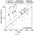
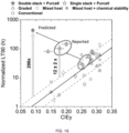
- Fig. 7C compares the normalized LT90 vs. CIE y from this work with previously reported blue Ir-complex-based PHOLEDs.
- a small CIE y coordinate is required for a blue pixel to reach the full color gamut in displays, although the normalized LT90 shows an exponential decrease in the total number of outcoupled photons during the device lifetime with CIE y due to a corresponding increase in exciton energy. As above, this results in a greater potential for excitons to engage in destructive bimolecular annihilation.
- deeper blue devices have substantially shorter lives than cyan-emitting PHOLEDs, making the challenge of achieving adequate lifetimes for deep blue devices increasingly more difficult.
- Past demonstrations have reduced the effects of energetically-driven degradation via spatial spreading of the triplet density profile by grading the EML doping or using mixed co-hosts in the EML, besides increasing chemical stability or steric hindrance to close packing of dopants and hosts to prevent their fragmentation.
- These efforts have increased the normalized LT90 from conventional, single host, uniformly doped devices by one order of magnitude.
- the cavity design is independent of the host matrix and emitter composition, it can be applied to a variety of structures and other triplet-dominated devices, including those based on exciplex forming cohost matrices.
- a deep blue, exciplex-forming co-host Ir(cb) 3 device achieved a 3.4-time device lifetime improvement compared to the control, see Fig. 13B .
- the fabrication of the bottom and the top cavity structures are non-intrusive of the OLED layers while following standard OLED fabrication and general lithography processes.
- the solutions presented here for bottom emitting devices can equally be applied to top emitting PHOLEDs with suitable changes in the cavity structure.
- the Purcell effect in PHOLEDs is significantly enhanced by polaritons through the plasmon-exciton polaritons (PEPs), thereby dramatically extending the operational lifetime of deep blue devices while maintaining a high EQE.
- PEPs plasmon-exciton polaritons
- Polariton dispersion and cavity engineering provides new degrees of freedom for the design of OLEDs. For example, an average Purcell factor of 2.4 ⁇ 0.2 via PEPs was achieved, leading to a maximum 5.3X lifetime enhancement compared to analogous, conventional PHOLEDs.
- a color shift was achieved from cyan to deep blue for Purcell-enhanced Ir(dmp) 3 devices without decreasing EQE or introducing noticeable angle dependence to the emission color.
- ⁇ ⁇ 0 ,p and h are the triplet transition dipole moment matrix element and the reduced Planck's constant, respectively.
- the ODoS is determined by the dyadic Green's function G(r 0 , r 0 ; ⁇ 0 ) by ⁇ p (r 0 , ⁇ 0 ) ⁇ n p ⁇ Im[G(r 0 , r 0 ; ⁇ 0 )] ⁇ n p ⁇ ⁇ k
- the PEPs and Ag-enhanced SPPs have a larger mode density
- PF is primarily controlled by the energy transfer rate to the polaritons at the metal/ETL interface.
- the PEP is due to coupling of excitons in the ETL with SPPs on the metal cathode.
- Ag has an absorption band starting from 3.8 eV that leads to the flattening of the high-k x plasmon modes.
- the Purcell effect prolongs the device operational lifetime by reducing the triplet density, thus slowing defect generation (and hence nonradiative quenching) via TPA and TTA.
- k tot , k nr , K TPA , K TTA and K QN are the total decay rate, the natural nonradiative decay rate, the defect generation rates due to TPA, TTA, and the bimolecular quenching rate between the triplets of density, N, and the defects of density, Q, respectively.
- the Purcell effect reduces the initial triplet density by 1/PF. This, in turn, reduces the initial rate of defect generation induced by TPA or TTA by 1/PF or 1/PF 2 , respectively .
- a larger defect density is required to match the increased radiative decay rates equivalent to that required prior to aging.
- the slowed defect generation and reduced quenching give rise to a power law m > 1 between the lifetime enhancement and PF in Eqs. (2)-(3).
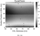
- the measured PL transients in Fig. 5B show a negligible change in low-Q Ag/DBR cavities. This is consistent with the dominance of the polariton ODoS, among outcoupled, substrate and waveguided modes in Fig. 11A . Due to the near-field nature of surface modes, the average PF is primarily controlled by the ETL thickness.
- the ETL is chosen for its large oscillator strength at wavelengths slightly shorter than the triplet emission wavelength. Therefore, the LP branch of the PEP is redshifted from the bare SPP due to its anti-crossing behavior.
- the dispersion and ODoS are tuned by the thickness of the ETL using transfer matrix and Green's function simulations.
- a higher ETL exciton energy than the dopant triplet energy prevents exciton leakage via Förster or Dexter energy transfer from the triplets, which reduces PHOLED efficiency.
- an ETL exciton energy close to the triplet energy increases the overlap between the PEP LP dispersion and the triplet emission spectra, leading to a large ODoS at the emission wavelengths. Therefore, an efficient ETL exciton with large oscillator strength at wavelengths slightly shorter than the triplet emission wavelength is optimal for exciting PEP-enhanced Purcell effects.
- Fig. 4 the PEP of a 20 nm AI/20 nm BPyTP2 bilayer is identified by angle-dependent reflectance spectroscopy.
- the measured AI/BPyTP2 PEP dispersions are extracted from the local minima with the linear background subtracted in Fig.
- H ⁇ k x / k 0 E SPP g 1 g 2 g 3 g 1 E ex1 0 0 g 2 0 E ex2 0 g 3 0 0 E ex3
- E SPP is the bare SPP dispersion
- g 1 , g 2 , and g 3 are the coupling strengths between the SPP mode and BPyTP2 0-0, 0-1, and 0-2 exciton vibronic states, respectively.
- g 1 and g 2 obtained from the spectral fits are 0.64 ⁇ 0.05 eV and 0.70 ⁇ 0.05 eV, respectively.
- the Rabi splitting energies for the 0-0 exciton and the 0-1 excitons are 1.3 ⁇ 0.1 eV and 1.4 ⁇ 0.1 eV, confirming that the strong coupling regime is reached.
- Ir(cb) 3 Operational lifetime improvements have also been found for PHOLEDs employing the deep blue but relatively short-lived phosphor, Ir(cb) 3 , in a mixed co-host mCBP:SiTrzCz2 EML . See Data Table 1 and Fig. 13B for detailed lifetime data.
- structures 4-6 employ a BPyTP2 ETL with thicknesses reduced from 40nm to 15nm for enhanced ET to the PEPs.
- the current-voltage characteristics show no change, see Fig. 13E .
- PHOLEDs were grown on glass substrates with pre-patterned bottom electrodes that were solvent-cleaned and treated by UV-ozone plasma for 15 min.
- the DBRs were grown by plasma-enhanced chemical vapor deposition (PECVD) at a temperature of 200°C.
- PECVD plasma-enhanced chemical vapor deposition
- the 50-60 nm thick indium-tin-oxide (ITO) layer was deposited via magnetron sputtering in an Ar plasma with a partial pressure of 2 mTorr at a deposition rate of 1.5 ⁇ /s.
- the thickness and number of pairs of the DBR are iterated to match the linewidth and spectral overlap of the phosphor emission spectrum.
- the SiN x /SiO 2 layer thicknesses are 56nm/80nm targeted at a central wavelength of 465nm, with 10% variation from batch to batch.
- the thicknesses of the ITO and SiN x capping layer are iterated to align the cavity modes with the phosphor emission spectrum.
- the ITO is rapid thermal annealed at 450°C under forming gas for 3 min (20-40 ⁇ /sq).
- the ITO is wet-etched in HCl: H 2 O (1:1 volume ratio) for 16 min with the electrode pattern protected by 3 ⁇ m thick S1813 photoresist.
- the organic layers are deposited by thermal evaporation in a vacuum chamber with a base pressure ⁇ 10 -7 torr.
- Fig. 8 The materials used, some of which are shown in Fig. 8 are: 2-(9,9'-spirobi[fluoren]-3-yl)-4,6-diphenyl-1,3,5-triazine (SF3Trz) 17 nm / 3,3'-Di(9H-carbazol-9-yl)-1,1'-biphenyl (mCBP) 5 nm / mCBP: iridium (III) tris[3-(2,6-dimethylphenyl)-7-methylimidazo[1,2-f] phenanthridine] (Ir(dmp) 3 ) 18-8 vol.% graded / N,N'-Di(1-naphthyl)-N,N'-diphenyl-(1,1'-biphenyl)-4,4'-diamine (NPD) + Dipyrazino[2,3-f:2',3'-h]quinoxaline-2,3,6,
- the cathodes are deposited using a thin metal shadow mask to define the 2 mm 2 device active area. All Al layers are deposited first at a rate of 0.1 ⁇ /s up to a thickness of 50 ⁇ , and then at 1 ⁇ /s until 100 nm total thickness is reached. All Ag layers are deposited at a rate of 0.1 ⁇ /s up to a thickness of 150 ⁇ , and then at 0.6 ⁇ /s until 100 nm total thickness is reached.
- the devices are encapsulated by a glass cover attached to the substrate using a bead of UV-cured epoxy around its periphery in a N 2 environment with O 2 / H 2 O concentrations ⁇ 0.1 ppm.
- the J-V, luminance and EQE characteristics are measured using a semiconductor parameter analyzer (B1500A, Keysight Technologies) and a calibrated, large-area photodiode (S3584-08, Hamamatsu Photonics) collecting all photons in the forward-viewing direction following standard procedures to eliminate errors due to the angular dependence of emission.
- the electroluminescence (EL) spectra are measured via a fiber-coupled spectrometer (USB4000, Ocean Optics, Inc.).
- the EQE data are taken from at least two different batches with at least two devices in each batch.
- Device operational lifetime is measured at a constant current density and room temperature.
- the luminance data are collected via automated source-measurement units (SMUs, Agilent, U2722 and Agilent, 34972A). Lifetime data are taken from at least two different batches comprising at least two devices.
- the optical structures are: 100 nm metal/ ⁇ nm ETL/ 5 nm SiTrzCz2/ 50nm mCBP: SiTrzCz2:Ir(cb) 3 (40:40:20 vol.
- the TrPL data for the full device structures are collected via a time-correlated single-photon counter (PicoHarp 300, PicoQuant) coupled to a microscope (Eclipse Ti2, Nikon).
- the pump laser (P-C-405, PicoQuant) wavelength is 405nm, with a repetition rate of 10 kHz, a pump power ⁇ 1nW and a beam diameter of 0.5 ⁇ m.
- the pump wavelength is selected to reach the maximum ratio of the phosphor-to-background emission in other organic layers such as BPyTP2.
- ⁇ , K TT and N 0 are the PL lifetime of the phosphor, triplet-triplet quenching rate, and the initial triplet density, respectively.
- the pump power is selected such that ⁇ K TT N 0 « 10% to avoid the effects of the bimolecular quenching.
- Angle-resolved reflectance is measured using ellipsometry (Woollam 2000, Woollam).
- the structures for Fig. 4 are: ETL 20nm / Al 20nm and ETL 20nm / Ag 40nm on a UV-fused silica prism coupler.
- the transfer matrix method is used to model the angle-resolved reflection of the multilayer structures.
- the Fourier image of the reflection and PL signal passes through an analyzer, reconstructed on the charge coupled device (PIXIS 1024B, Teledyne Princeton Instruments) and resolved by a spectrograph (HRS500, Teledyne Princeton Instruments).
- All angle-resolved PL spectra in Fig. 4C are pumped by a 405 nm wavelength, 1 kHz ns-pulsed laser with a fluence of 1 J/cm 2 and integrated for 1 min.
- the signal is filtered by a 425 nm long-pass filter placed before the monochromator.
- Optical constants are measured from 250 -1700 nm using an ellipsometer (Woollam 2000, Woollam) and averaged over several thin films (20 - 50 nm) on Si/SiO 2 substrates fit to B-spline and general oscillator models.
- the extinction coefficient, k is iterated by comparing it to the UV-Vis spectra (Perkin Elmer 1050) of the same thin films on sapphire substrates.
- the dyadic Green's function method follows Celebi et al. based on a dipole embedded in a multilayer structure.
- the OLED structure determines the multimode expansion of the Green's function, and thereby, the electrical field and OdoS.
- the dissipated power simulated by taking the real part of the Poynting vector, is proportional to the decay rate of the dipole, and thus proportional is to the OdoS.
- the optical modes are outcoupled modes (including outcoupled cavity modes), substrate modes, waveguide modes, and SPP/PEP modes, among others.
- the Purcell factor and energy transfer rates are calculated through the OdoS and dissipated radiative power of each mode.
- the PF is the total OdoS, ⁇ tot ( ⁇ k ), of a dipole normalized by that of a dipole in an isotropic, infinite medium of the EML.
- the outcoupling efficiency is calculated from the dissipated power through modes with k x /k 0 ⁇ 1 normalized to the total OdoS ⁇ tot ( ⁇ k ).
- the average PF of each device is calculated from the overlap of the emission spectra of Ir(dmp) 3 and a uniform exciton spatial distribution assuming isotropic dipole orientation.
- PEPs plasmon-exciton polaritons
- ETL electron transporting layer
- HTL hole transporting layer
- ETL electron transporting layer
- Two exemplary ETL and HTL materials showed the PEPs.
- the PEPs featured a flat dispersion in the lower polariton branch, and a high optical density of states (OdoS) in the blue visible region.
- the polariton dispersion and OdoS was engineered to match the final emitter spectrally in the near-field to maximize the radiative decay rates.
- the metal-metal cavity was designed for optimizing outcoupling efficiency and the polariton-enhanced Purcell effect by placing the emission layers (EMLs) at the antinodes of metal-metal cavity mode and close to the metal surface.
- EMLs emission layers
- An example of a stacked blue OLED using Purcell effect enhancement that was explored comprised of Ag 100nm /Al 3nm/ Liq 1.5nm/ BpyTP2 15-20nm/ mSiTrz 5nm/ SiCzCz:SiTrzCz2 (1:1):PtON-TBBi 6-13 vol% 50-60nm /SiCzCz 5nm/BCFN 5-30 nm/HATCN 10nm/BpyTP2:Li 50:50 mol % 12nm / BpyTP2 8-30 nm/ mSiTrz 5nm/ SiCzCz:SiTrzCz2 (1:1):PtON-TBBi 6-13 vol% 50-60nm /SiCzCz 5nm/BCFN 5nm/ HATCN 5nm/ ITO 5-20nm /Al, Ti, TiO 2 or NiCr 2-3nm/Ag 16-20nm/ Ti, TiO
- Another example of a stacked blue OLED using Purcell effect enhancement comprised of Ag 100nm /Al 3nm/ Liq 1.5nm/ BpyTP2 15-20nm/ mCBP 5nm/ mCBP:Ir(dmp) 3 doped 18-8 vol% 50-60nm /BCFN 5-30 nm/HATCN 10nm/BpyTP2:Li 50:50 mol % 12nm / BpyTP2 8-30 nm/ mCBP 5nm/ mCBP:Ir(dmp) 3 doped 18-8 vol% 50-60nm /BCFN 5nm/ HATCN 5nm/ ITO 5-20nm /Al, Ti, TiO 2 or NiCr 2-3nm/Ag 16-20nm/Ti, TiO 2 or NiCr 2-3nm/ITO 20-70nm/Glass.
- the ETL, HTL and/or HIL had large extinction coefficient right above 400-450 nm, typically in the range of 300-400 nm.
- the criteria for the large extinction coefficient are when the material is adjacent to the metal electrode, an anti-crossing forms between the metal electrode surface plasmon polaritons (SPPs) and the material excitonic absorption, forming plasmon-exciton-polaritons (PEPs).
- SPPs surface plasmon polaritons
- PEPs plasmon-exciton-polaritons
- Such materials include BpyTP2 (ETL), BCFN (HTL), and anthracene-based ETL material including MADN, ZADN and TBADN etc. Examples of PEPs are in Figs. 14A-14F .
- the stacked device lifetime enhancement originated both from the Purcell effect and lower driving current density by stacking EMLs.
- the simulated Purcell factor and outcoupling efficiency are shown in Figs. 15A-15C .
- the optimized Purcell factor was >2.4 and outcoupling efficiency was >25%.
- PFs of horizontal and vertical dipoles are PF horiz . and PF vert. , respectively.
Landscapes
- Physics & Mathematics (AREA)
- Optics & Photonics (AREA)
- Electroluminescent Light Sources (AREA)
Applications Claiming Priority (7)
| Application Number | Priority Date | Filing Date | Title |
|---|---|---|---|
| US202363482186P | 2023-01-30 | 2023-01-30 | |
| US202363495197P | 2023-04-10 | 2023-04-10 | |
| US202363510702P | 2023-06-28 | 2023-06-28 | |
| US202363512966P | 2023-07-11 | 2023-07-11 | |
| US202363610024P | 2023-12-14 | 2023-12-14 | |
| US202363613961P | 2023-12-22 | 2023-12-22 | |
| US18/413,235 US20240268139A1 (en) | 2023-01-30 | 2024-01-16 | Organic electroluminescent devices |
Publications (2)
| Publication Number | Publication Date |
|---|---|
| EP4408139A2 true EP4408139A2 (de) | 2024-07-31 |
| EP4408139A3 EP4408139A3 (de) | 2024-08-14 |
Family
ID=89772016
Family Applications (1)
| Application Number | Title | Priority Date | Filing Date |
|---|---|---|---|
| EP24154647.2A Pending EP4408139A3 (de) | 2023-01-30 | 2024-01-30 | Organische elektrolumineszente vorrichtungen |
Country Status (3)
| Country | Link |
|---|---|
| US (1) | US20240268139A1 (de) |
| EP (1) | EP4408139A3 (de) |
| KR (1) | KR20240119851A (de) |
Citations (19)
| Publication number | Priority date | Publication date | Assignee | Title |
|---|---|---|---|---|
| US4769292A (en) | 1987-03-02 | 1988-09-06 | Eastman Kodak Company | Electroluminescent device with modified thin film luminescent zone |
| US5247190A (en) | 1989-04-20 | 1993-09-21 | Cambridge Research And Innovation Limited | Electroluminescent devices |
| US5703436A (en) | 1994-12-13 | 1997-12-30 | The Trustees Of Princeton University | Transparent contacts for organic devices |
| US5707745A (en) | 1994-12-13 | 1998-01-13 | The Trustees Of Princeton University | Multicolor organic light emitting devices |
| US5834893A (en) | 1996-12-23 | 1998-11-10 | The Trustees Of Princeton University | High efficiency organic light emitting devices with light directing structures |
| US5844363A (en) | 1997-01-23 | 1998-12-01 | The Trustees Of Princeton Univ. | Vacuum deposited, non-polymeric flexible organic light emitting devices |
| US6013982A (en) | 1996-12-23 | 2000-01-11 | The Trustees Of Princeton University | Multicolor display devices |
| US6087196A (en) | 1998-01-30 | 2000-07-11 | The Trustees Of Princeton University | Fabrication of organic semiconductor devices using ink jet printing |
| US6091195A (en) | 1997-02-03 | 2000-07-18 | The Trustees Of Princeton University | Displays having mesa pixel configuration |
| US6097147A (en) | 1998-09-14 | 2000-08-01 | The Trustees Of Princeton University | Structure for high efficiency electroluminescent device |
| US6294398B1 (en) | 1999-11-23 | 2001-09-25 | The Trustees Of Princeton University | Method for patterning devices |
| US6303238B1 (en) | 1997-12-01 | 2001-10-16 | The Trustees Of Princeton University | OLEDs doped with phosphorescent compounds |
| US6337102B1 (en) | 1997-11-17 | 2002-01-08 | The Trustees Of Princeton University | Low pressure vapor phase deposition of organic thin films |
| US20030230980A1 (en) | 2002-06-18 | 2003-12-18 | Forrest Stephen R | Very low voltage, high efficiency phosphorescent oled in a p-i-n structure |
| US20040174116A1 (en) | 2001-08-20 | 2004-09-09 | Lu Min-Hao Michael | Transparent electrodes |
| US7279704B2 (en) | 2004-05-18 | 2007-10-09 | The University Of Southern California | Complexes with tridentate ligands |
| US7431968B1 (en) | 2001-09-04 | 2008-10-07 | The Trustees Of Princeton University | Process and apparatus for organic vapor jet deposition |
| US7968146B2 (en) | 2006-11-01 | 2011-06-28 | The Trustees Of Princeton University | Hybrid layers for use in coatings on electronic devices or other articles |
| US20170229663A1 (en) | 2016-02-09 | 2017-08-10 | Universal Display Corporation | Organic electroluminescent materials and devices |
Family Cites Families (4)
| Publication number | Priority date | Publication date | Assignee | Title |
|---|---|---|---|---|
| US11569480B2 (en) * | 2019-03-12 | 2023-01-31 | Universal Display Corporation | Plasmonic OLEDs and vertical dipole emitters |
| JPWO2022034916A1 (de) * | 2020-08-12 | 2022-02-17 | ||
| US20220271260A1 (en) * | 2021-02-23 | 2022-08-25 | The Regents Of The University Of Michigan | Organic light emitting device |
| US20230255047A1 (en) * | 2022-01-21 | 2023-08-10 | The Regents Of The University Of Michigan | Enhanced purcell effect using red-shifted surface plasmon modes and high index material in organic light emitting devices |
-
2024
- 2024-01-16 US US18/413,235 patent/US20240268139A1/en active Pending
- 2024-01-30 KR KR1020240013706A patent/KR20240119851A/ko active Pending
- 2024-01-30 EP EP24154647.2A patent/EP4408139A3/de active Pending
Patent Citations (20)
| Publication number | Priority date | Publication date | Assignee | Title |
|---|---|---|---|---|
| US4769292A (en) | 1987-03-02 | 1988-09-06 | Eastman Kodak Company | Electroluminescent device with modified thin film luminescent zone |
| US5247190A (en) | 1989-04-20 | 1993-09-21 | Cambridge Research And Innovation Limited | Electroluminescent devices |
| US5703436A (en) | 1994-12-13 | 1997-12-30 | The Trustees Of Princeton University | Transparent contacts for organic devices |
| US5707745A (en) | 1994-12-13 | 1998-01-13 | The Trustees Of Princeton University | Multicolor organic light emitting devices |
| US5834893A (en) | 1996-12-23 | 1998-11-10 | The Trustees Of Princeton University | High efficiency organic light emitting devices with light directing structures |
| US6013982A (en) | 1996-12-23 | 2000-01-11 | The Trustees Of Princeton University | Multicolor display devices |
| US5844363A (en) | 1997-01-23 | 1998-12-01 | The Trustees Of Princeton Univ. | Vacuum deposited, non-polymeric flexible organic light emitting devices |
| US6091195A (en) | 1997-02-03 | 2000-07-18 | The Trustees Of Princeton University | Displays having mesa pixel configuration |
| US6337102B1 (en) | 1997-11-17 | 2002-01-08 | The Trustees Of Princeton University | Low pressure vapor phase deposition of organic thin films |
| US6303238B1 (en) | 1997-12-01 | 2001-10-16 | The Trustees Of Princeton University | OLEDs doped with phosphorescent compounds |
| US6087196A (en) | 1998-01-30 | 2000-07-11 | The Trustees Of Princeton University | Fabrication of organic semiconductor devices using ink jet printing |
| US6097147A (en) | 1998-09-14 | 2000-08-01 | The Trustees Of Princeton University | Structure for high efficiency electroluminescent device |
| US6294398B1 (en) | 1999-11-23 | 2001-09-25 | The Trustees Of Princeton University | Method for patterning devices |
| US6468819B1 (en) | 1999-11-23 | 2002-10-22 | The Trustees Of Princeton University | Method for patterning organic thin film devices using a die |
| US20040174116A1 (en) | 2001-08-20 | 2004-09-09 | Lu Min-Hao Michael | Transparent electrodes |
| US7431968B1 (en) | 2001-09-04 | 2008-10-07 | The Trustees Of Princeton University | Process and apparatus for organic vapor jet deposition |
| US20030230980A1 (en) | 2002-06-18 | 2003-12-18 | Forrest Stephen R | Very low voltage, high efficiency phosphorescent oled in a p-i-n structure |
| US7279704B2 (en) | 2004-05-18 | 2007-10-09 | The University Of Southern California | Complexes with tridentate ligands |
| US7968146B2 (en) | 2006-11-01 | 2011-06-28 | The Trustees Of Princeton University | Hybrid layers for use in coatings on electronic devices or other articles |
| US20170229663A1 (en) | 2016-02-09 | 2017-08-10 | Universal Display Corporation | Organic electroluminescent materials and devices |
Non-Patent Citations (28)
Also Published As
| Publication number | Publication date |
|---|---|
| EP4408139A3 (de) | 2024-08-14 |
| US20240268139A1 (en) | 2024-08-08 |
| KR20240119851A (ko) | 2024-08-06 |
Similar Documents
| Publication | Publication Date | Title |
|---|---|---|
| KR102850072B1 (ko) | 표면-플라즈몬-펌핑된 발광 디바이스 | |
| Lee et al. | Highly efficient, color-reproducible full-color electroluminescent devices based on red/green/blue quantum dot-mixed multilayer | |
| KR102819737B1 (ko) | Oled 구조에서 tamm 플라즈몬 스택을 통한 퍼셀 개선 | |
| CN112242493B (zh) | 有机发光装置 | |
| US20240172462A1 (en) | Organic electroluminescent devices | |
| US20220271260A1 (en) | Organic light emitting device | |
| US20250133896A1 (en) | Organic electroluminescent devices | |
| EP4408139A2 (de) | Organische elektrolumineszente vorrichtungen | |
| US20250081720A1 (en) | Organic electroluminescent devices | |
| CN117956821A (zh) | 有机电致发光材料和装置 | |
| US20260082766A1 (en) | Organic electroluminescent devices | |
| CN118414013A (zh) | 有机电致发光装置 | |
| CN113921728A (zh) | 等离激元oled和垂直偶极子发射体 | |
| US20250008764A1 (en) | Organic electroluminescent devices | |
| US20240180025A1 (en) | Organic electroluminescent materials and devices | |
| US20250151562A1 (en) | Organic electroluminescent devices | |
| US20250024696A1 (en) | Organic electroluminescent devices | |
| US20240196730A1 (en) | Organic electroluminescent materials and devices | |
| US20260082763A1 (en) | Organic electroluminescent devices | |
| US20240147754A1 (en) | Organic Electroluminescent Devices | |
| US20240180024A1 (en) | Organic electroluminescent materials and devices | |
| US20240373710A1 (en) | Organic electroluminescent devices | |
| US20230091551A1 (en) | White organic light emitting device with stable spectrum employing transport barrier layers | |
| US20230042189A1 (en) | Integrated oled lighting for automobile applications | |
| KR20260044823A (ko) | 유기 전계발광 디바이스 |
Legal Events
| Date | Code | Title | Description |
|---|---|---|---|
| PUAI | Public reference made under article 153(3) epc to a published international application that has entered the european phase |
Free format text: ORIGINAL CODE: 0009012 |
|
| STAA | Information on the status of an ep patent application or granted ep patent |
Free format text: STATUS: THE APPLICATION HAS BEEN PUBLISHED |
|
| PUAL | Search report despatched |
Free format text: ORIGINAL CODE: 0009013 |
|
| AK | Designated contracting states |
Kind code of ref document: A2 Designated state(s): AL AT BE BG CH CY CZ DE DK EE ES FI FR GB GR HR HU IE IS IT LI LT LU LV MC ME MK MT NL NO PL PT RO RS SE SI SK SM TR |
|
| AK | Designated contracting states |
Kind code of ref document: A3 Designated state(s): AL AT BE BG CH CY CZ DE DK EE ES FI FR GB GR HR HU IE IS IT LI LT LU LV MC ME MK MT NL NO PL PT RO RS SE SI SK SM TR |
|
| RIC1 | Information provided on ipc code assigned before grant |
Ipc: H10K 101/10 20230101ALN20240709BHEP Ipc: H10K 50/85 20230101ALI20240709BHEP Ipc: H10K 50/852 20230101AFI20240709BHEP |
|
| STAA | Information on the status of an ep patent application or granted ep patent |
Free format text: STATUS: REQUEST FOR EXAMINATION WAS MADE |
|
| 17P | Request for examination filed |
Effective date: 20250211 |