EP4408138A1 - Organic light emitting device - Google Patents
Organic light emitting device Download PDFInfo
- Publication number
- EP4408138A1 EP4408138A1 EP23220557.5A EP23220557A EP4408138A1 EP 4408138 A1 EP4408138 A1 EP 4408138A1 EP 23220557 A EP23220557 A EP 23220557A EP 4408138 A1 EP4408138 A1 EP 4408138A1
- Authority
- EP
- European Patent Office
- Prior art keywords
- thickness
- layer
- blue
- anode
- green
- Prior art date
- Legal status (The legal status is an assumption and is not a legal conclusion. Google has not performed a legal analysis and makes no representation as to the accuracy of the status listed.)
- Pending
Links
Images

Classifications
-
- H—ELECTRICITY
- H10—SEMICONDUCTOR DEVICES; ELECTRIC SOLID-STATE DEVICES NOT OTHERWISE PROVIDED FOR
- H10K—ORGANIC ELECTRIC SOLID-STATE DEVICES
- H10K59/00—Integrated devices, or assemblies of multiple devices, comprising at least one organic light-emitting element covered by group H10K50/00
- H10K59/80—Constructional details
- H10K59/875—Arrangements for extracting light from the devices
- H10K59/876—Arrangements for extracting light from the devices comprising a resonant cavity structure, e.g. Bragg reflector pair
-
- H—ELECTRICITY
- H10—SEMICONDUCTOR DEVICES; ELECTRIC SOLID-STATE DEVICES NOT OTHERWISE PROVIDED FOR
- H10K—ORGANIC ELECTRIC SOLID-STATE DEVICES
- H10K50/00—Organic light-emitting devices
- H10K50/10—OLEDs or polymer light-emitting diodes [PLED]
- H10K50/11—OLEDs or polymer light-emitting diodes [PLED] characterised by the electroluminescent [EL] layers
- H10K50/125—OLEDs or polymer light-emitting diodes [PLED] characterised by the electroluminescent [EL] layers specially adapted for multicolour light emission, e.g. for emitting white light
-
- H—ELECTRICITY
- H10—SEMICONDUCTOR DEVICES; ELECTRIC SOLID-STATE DEVICES NOT OTHERWISE PROVIDED FOR
- H10K—ORGANIC ELECTRIC SOLID-STATE DEVICES
- H10K59/00—Integrated devices, or assemblies of multiple devices, comprising at least one organic light-emitting element covered by group H10K50/00
- H10K59/30—Devices specially adapted for multicolour light emission
- H10K59/35—Devices specially adapted for multicolour light emission comprising red-green-blue [RGB] subpixels
-
- G—PHYSICS
- G09—EDUCATION; CRYPTOGRAPHY; DISPLAY; ADVERTISING; SEALS
- G09F—DISPLAYING; ADVERTISING; SIGNS; LABELS OR NAME-PLATES; SEALS
- G09F9/00—Indicating arrangements for variable information in which the information is built-up on a support by selection or combination of individual elements
- G09F9/30—Indicating arrangements for variable information in which the information is built-up on a support by selection or combination of individual elements in which the desired character or characters are formed by combining individual elements
- G09F9/33—Indicating arrangements for variable information in which the information is built-up on a support by selection or combination of individual elements in which the desired character or characters are formed by combining individual elements being semiconductor devices, e.g. diodes
- G09F9/335—Indicating arrangements for variable information in which the information is built-up on a support by selection or combination of individual elements in which the desired character or characters are formed by combining individual elements being semiconductor devices, e.g. diodes being organic light emitting diodes [OLED]
-
- H—ELECTRICITY
- H10—SEMICONDUCTOR DEVICES; ELECTRIC SOLID-STATE DEVICES NOT OTHERWISE PROVIDED FOR
- H10K—ORGANIC ELECTRIC SOLID-STATE DEVICES
- H10K50/00—Organic light-emitting devices
- H10K50/10—OLEDs or polymer light-emitting diodes [PLED]
- H10K50/11—OLEDs or polymer light-emitting diodes [PLED] characterised by the electroluminescent [EL] layers
- H10K50/125—OLEDs or polymer light-emitting diodes [PLED] characterised by the electroluminescent [EL] layers specially adapted for multicolour light emission, e.g. for emitting white light
- H10K50/13—OLEDs or polymer light-emitting diodes [PLED] characterised by the electroluminescent [EL] layers specially adapted for multicolour light emission, e.g. for emitting white light comprising stacked EL layers within one EL unit
-
- H—ELECTRICITY
- H10—SEMICONDUCTOR DEVICES; ELECTRIC SOLID-STATE DEVICES NOT OTHERWISE PROVIDED FOR
- H10K—ORGANIC ELECTRIC SOLID-STATE DEVICES
- H10K50/00—Organic light-emitting devices
- H10K50/10—OLEDs or polymer light-emitting diodes [PLED]
- H10K50/11—OLEDs or polymer light-emitting diodes [PLED] characterised by the electroluminescent [EL] layers
- H10K50/125—OLEDs or polymer light-emitting diodes [PLED] characterised by the electroluminescent [EL] layers specially adapted for multicolour light emission, e.g. for emitting white light
- H10K50/13—OLEDs or polymer light-emitting diodes [PLED] characterised by the electroluminescent [EL] layers specially adapted for multicolour light emission, e.g. for emitting white light comprising stacked EL layers within one EL unit
- H10K50/131—OLEDs or polymer light-emitting diodes [PLED] characterised by the electroluminescent [EL] layers specially adapted for multicolour light emission, e.g. for emitting white light comprising stacked EL layers within one EL unit with spacer layers between the electroluminescent layers
-
- H—ELECTRICITY
- H10—SEMICONDUCTOR DEVICES; ELECTRIC SOLID-STATE DEVICES NOT OTHERWISE PROVIDED FOR
- H10K—ORGANIC ELECTRIC SOLID-STATE DEVICES
- H10K50/00—Organic light-emitting devices
- H10K50/10—OLEDs or polymer light-emitting diodes [PLED]
- H10K50/14—Carrier transporting layers
- H10K50/15—Hole transporting layers
-
- H—ELECTRICITY
- H10—SEMICONDUCTOR DEVICES; ELECTRIC SOLID-STATE DEVICES NOT OTHERWISE PROVIDED FOR
- H10K—ORGANIC ELECTRIC SOLID-STATE DEVICES
- H10K50/00—Organic light-emitting devices
- H10K50/10—OLEDs or polymer light-emitting diodes [PLED]
- H10K50/14—Carrier transporting layers
- H10K50/16—Electron transporting layers
-
- H—ELECTRICITY
- H10—SEMICONDUCTOR DEVICES; ELECTRIC SOLID-STATE DEVICES NOT OTHERWISE PROVIDED FOR
- H10K—ORGANIC ELECTRIC SOLID-STATE DEVICES
- H10K50/00—Organic light-emitting devices
- H10K50/10—OLEDs or polymer light-emitting diodes [PLED]
- H10K50/17—Carrier injection layers
-
- H—ELECTRICITY
- H10—SEMICONDUCTOR DEVICES; ELECTRIC SOLID-STATE DEVICES NOT OTHERWISE PROVIDED FOR
- H10K—ORGANIC ELECTRIC SOLID-STATE DEVICES
- H10K50/00—Organic light-emitting devices
- H10K50/10—OLEDs or polymer light-emitting diodes [PLED]
- H10K50/17—Carrier injection layers
- H10K50/171—Electron injection layers
-
- H—ELECTRICITY
- H10—SEMICONDUCTOR DEVICES; ELECTRIC SOLID-STATE DEVICES NOT OTHERWISE PROVIDED FOR
- H10K—ORGANIC ELECTRIC SOLID-STATE DEVICES
- H10K50/00—Organic light-emitting devices
- H10K50/10—OLEDs or polymer light-emitting diodes [PLED]
- H10K50/19—Tandem OLEDs
-
- H—ELECTRICITY
- H10—SEMICONDUCTOR DEVICES; ELECTRIC SOLID-STATE DEVICES NOT OTHERWISE PROVIDED FOR
- H10K—ORGANIC ELECTRIC SOLID-STATE DEVICES
- H10K50/00—Organic light-emitting devices
- H10K50/80—Constructional details
- H10K50/805—Electrodes
- H10K50/81—Anodes
- H10K50/813—Anodes characterised by their shape
-
- H—ELECTRICITY
- H10—SEMICONDUCTOR DEVICES; ELECTRIC SOLID-STATE DEVICES NOT OTHERWISE PROVIDED FOR
- H10K—ORGANIC ELECTRIC SOLID-STATE DEVICES
- H10K59/00—Integrated devices, or assemblies of multiple devices, comprising at least one organic light-emitting element covered by group H10K50/00
- H10K59/10—OLED displays
- H10K59/12—Active-matrix OLED [AMOLED] displays
-
- H—ELECTRICITY
- H10—SEMICONDUCTOR DEVICES; ELECTRIC SOLID-STATE DEVICES NOT OTHERWISE PROVIDED FOR
- H10K—ORGANIC ELECTRIC SOLID-STATE DEVICES
- H10K59/00—Integrated devices, or assemblies of multiple devices, comprising at least one organic light-emitting element covered by group H10K50/00
- H10K59/30—Devices specially adapted for multicolour light emission
- H10K59/32—Stacked devices having two or more layers, each emitting at different wavelengths
-
- H—ELECTRICITY
- H10—SEMICONDUCTOR DEVICES; ELECTRIC SOLID-STATE DEVICES NOT OTHERWISE PROVIDED FOR
- H10K—ORGANIC ELECTRIC SOLID-STATE DEVICES
- H10K59/00—Integrated devices, or assemblies of multiple devices, comprising at least one organic light-emitting element covered by group H10K50/00
- H10K59/30—Devices specially adapted for multicolour light emission
- H10K59/35—Devices specially adapted for multicolour light emission comprising red-green-blue [RGB] subpixels
- H10K59/353—Devices specially adapted for multicolour light emission comprising red-green-blue [RGB] subpixels characterised by the geometrical arrangement of the RGB subpixels
-
- H—ELECTRICITY
- H10—SEMICONDUCTOR DEVICES; ELECTRIC SOLID-STATE DEVICES NOT OTHERWISE PROVIDED FOR
- H10K—ORGANIC ELECTRIC SOLID-STATE DEVICES
- H10K59/00—Integrated devices, or assemblies of multiple devices, comprising at least one organic light-emitting element covered by group H10K50/00
- H10K59/30—Devices specially adapted for multicolour light emission
- H10K59/38—Devices specially adapted for multicolour light emission comprising colour filters or colour changing media [CCM]
-
- H—ELECTRICITY
- H10—SEMICONDUCTOR DEVICES; ELECTRIC SOLID-STATE DEVICES NOT OTHERWISE PROVIDED FOR
- H10K—ORGANIC ELECTRIC SOLID-STATE DEVICES
- H10K59/00—Integrated devices, or assemblies of multiple devices, comprising at least one organic light-emitting element covered by group H10K50/00
- H10K59/80—Constructional details
- H10K59/805—Electrodes
- H10K59/8051—Anodes
-
- H—ELECTRICITY
- H10—SEMICONDUCTOR DEVICES; ELECTRIC SOLID-STATE DEVICES NOT OTHERWISE PROVIDED FOR
- H10K—ORGANIC ELECTRIC SOLID-STATE DEVICES
- H10K59/00—Integrated devices, or assemblies of multiple devices, comprising at least one organic light-emitting element covered by group H10K50/00
- H10K59/80—Constructional details
- H10K59/805—Electrodes
- H10K59/8051—Anodes
- H10K59/80515—Anodes characterised by their shape
-
- H—ELECTRICITY
- H10—SEMICONDUCTOR DEVICES; ELECTRIC SOLID-STATE DEVICES NOT OTHERWISE PROVIDED FOR
- H10K—ORGANIC ELECTRIC SOLID-STATE DEVICES
- H10K2102/00—Constructional details relating to the organic devices covered by this subclass
- H10K2102/301—Details of OLEDs
- H10K2102/351—Thickness
Definitions
- the present disclosure relates to an organic light emitting device, and more specifically, to an organic light emitting device having high emitting efficiency and high color gamut (color reproductivity).
- an organic light emitting display device including an OLED has been the subject of recent research and development.
- the OLED emits light by injecting electrons from a cathode as an electron injection electrode and holes from an anode as a hole injection electrode into an emitting material layer (EML), combining the electrons with the holes, generating an exciton, and transforming the exciton from an excited state to a ground state.
- a flexible substrate for example, a plastic substrate, can be used as a base substrate where elements are formed.
- the organic light emitting display device can be operated at a voltage (e.g., 10V or below) lower than a voltage required to operate other display devices.
- the organic light emitting display device has advantages in the power consumption and the color sense.
- a white OLED including a first emitting part, which includes a blue EML, a second emitting part, which includes a red EML and a green EML, and a third emitting part, which includes a blue EML, is introduced.
- a color uniformity is degraded by the first and third emitting parts each including the blue EML.
- the present disclosure is directed to an organic light emitting device that substantially obviates one or more of the problems associated with the limitations and disadvantages of the related conventional art.
- an aspect of the present disclosure is an organic light emitting display device comprising a substrate including red, green and blue pixel regions; and an organic light emitting diode including an anode, a cathode over the anode and an organic emitting layer between the anode and the cathode and corresponding to in the red, green and blue pixel regions, wherein the organic emitting layer includes a first emitting part including a red emitting material layer, a second emitting part including a green emitting material layer and positioned between the first emitting part and the cathode and a third emitting part including a blue emitting material layer and positioned between the second emitting part and the cathode, and wherein the anode in the blue pixel region has a first thickness, and the anode in the green pixel region has a second thickness being 2/5 to 2/3 of the first thickness.
- the first thickness may be 1/4 of a blue wavelength in the anode, the blue wavelength in the anode means ⁇ B /n, wherein ⁇ B is a wavelength of the blue light, n is a refractive index of the anode.
- the first thickness may be in a range of 500 to 600 ⁇ .
- the second thickness may be in a range of 200 to 400 ⁇ .
- a distance between a lower surface of the green emitting material layer and a lower surface of the cathode may be in a range of 180 to 230nm.
- a distance between a lower surface of the blue emitting material layer and a lower surface of the cathode may be in a range of 45 to 65nm.
- a distance between a lower surface of the red emitting material layer and a lower surface of the cathode may be in a range of 415 to 445nm.
- the first emitting part may further include a first hole transporting layer under the red emitting material layer, a hole injection layer under the first hole transporting layer and a first electron transporting layer on the red emitting material layer.
- the second emitting part may further include a second hole transporting layer under the green emitting material layer and a second electron transporting layer on the green emitting material layer.
- the third emitting part may further include a third hole transporting layer under the blue emitting material layer, a third electron transporting layer on the blue emitting material layer and an electron injection layer on the third electron transporting layer.
- a thickness of the third hole transporting layer may be greater than a thickness of the first hole transporting layer and/or may be smaller than a thickness of the second hole transporting layer.
- the thickness of the second hole transporting layer may be in a range of 125 to 165nm.
- the thickness of the third hole transporting layer may be in a range of 45 to 85nm.
- the thickness of the first hole transporting layer may be in a range of 25 to 35nm.
- the thickness of the second hole transporting layer may be in a range of 125 to 165nm.
- the thickness of the third hole transporting layer may be in a range of 45 to 85nm.
- a thickness of the first electron transporting layer may be greater than a thickness of the second electron transporting layer and/or may be smaller than a thickness of the third electron transporting layer.
- the thickness of the first electron transporting layer may be a range of 20 to 30nm.
- the thickness of the second electron transporting layer may be a range of 15 to 25nm.
- the thickness of the third electron transporting layer may be a range of 25 to 35nm.
- the anode in the red pixel region may have a third thickness being same as the first thickness or the second thickness.
- the organic emitting layer further may include a first charge generation layer between the first and second emitting parts and a second charge generation layer between the second and third emitting parts.
- the organic light emitting device may comprise a color filter layer corresponding to the red, green and blue pixel regions and positioned between the substrate and the organic light emitting diode.
- the element In construing an element, the element is construed as including an error or tolerance range although there is no explicit description of such an error or tolerance range.
- an organic light emitting device including the OLED may be an organic light emitting display device or an organic lightening device.
- an organic light emitting display device which is a display device including the OLED of the present disclosure, will be mainly described.
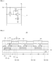
- FIG. 1 is a schematic circuit diagram illustrating an organic light emitting display device of the present disclosure.
- a gate line GL and a data line DL, which cross each other to define a pixel region (pixel) P, and a power line PL are formed in an organic light emitting display device.
- a switching thin film transistor (TFT) Ts, a driving TFT Td, a storage capacitor Cst and an OLED D are formed in the pixel region P.
- the pixel region P may include a red pixel region, a green pixel region and a blue pixel region.
- the switching thin film transistor Ts is connected to the gate line GL and the data line DL, and the driving thin film transistor Td is connected between the switching thin film transistor Ts and the power line PL.
- the storage capacitor Cst is connected to a gate electrode and a drain electrode of the driving TFT Td, and the OLED D is connected to the driving thin film transistor Td.
- the switching thin film transistor Ts When the switching thin film transistor Ts is turned on by the gate signal applied through the gate line GL, the data signal applied through the data line DL is applied into a gate electrode of the driving thin film transistor Td and one electrode of the storage capacitor Cst through the switching thin film transistor Ts.
- the driving thin film transistor Td is turned on by the data signal applied into the gate electrode so that a current proportional to the data signal is supplied from the power line PL to the OLED D through the driving thin film transistor Td.
- the OLED D emits light having a luminance proportional to the current flowing through the driving thin film transistor Td.
- the storage capacitor Cst is charge with a voltage proportional to the data signal so that the voltage of the gate electrode in the driving thin film transistor Td is kept constant during one frame.
- the organic light emitting display device can display a desired image.
- FIG. 2 is a schematic cross-sectional view illustrating an organic light emitting display device according to the present disclosure.
- the organic light emitting display device 100 includes a substrate 110, where a red pixel region RP, a green pixel region GP and a blue pixel region BP are defined, a TFT Tr on the substrate 110, an OLED D, which is disposed over the TFT Tr and connected to the TFT Tr, and a color filter layer 180 between the substrate 110 and the OLED D.
- the substrate 110 may be a glass substrate or a flexible substrate.
- the substrate 110 may be a polyimide (PI) substrate, a polyethersulfone (PES) substrate, a polyethylenenaphthalate (PEN) substrate, a polyethylene terephthalate (PET) substrate or a polycarbonate (PC) substrate.
- PI polyimide
- PES polyethersulfone
- PEN polyethylenenaphthalate
- PET polyethylene terephthalate
- PC polycarbonate
- a buffer layer 120 is formed on the substrate, and the TFT Tr, which respectively corresponds to the red, green and blue pixels RP, GP and BP, is formed on the buffer layer 120.
- the buffer layer 120 may be omitted, and the TFT Tr may be positioned on the substrate 110.
- a semiconductor layer 122 is formed on the buffer layer 120.
- the semiconductor layer 122 may include an oxide semiconductor material or polycrystalline silicon.
- a light-shielding pattern (not shown) may be formed under the semiconductor layer 122. The light to the semiconductor layer 122 is shielded or blocked by the light-shielding pattern such that thermal degradation of the semiconductor layer 122 can be prevented.
- impurities may be doped into both sides of the semiconductor layer 122.
- a gate insulating layer 124 of an insulating material is formed on the semiconductor layer 122 and over an entire surface of the substrate 110.
- the gate insulating layer 124 may be formed of an inorganic insulating material such as silicon oxide (SiOx) or silicon nitride (SiNx).
- a gate electrode 130 which is formed of a conductive material, e.g., metal, is formed on the gate insulating layer 124 to correspond to a center of the semiconductor layer 122.
- the gate insulating layer 124 is formed on an entire surface of the substrate 110.
- the gate insulating layer 124 may be patterned to have the same shape as the gate electrode 130.
- An interlayer insulating layer 132 which is formed of an insulating material, is formed on the gate electrode 130 and over an entire surface of the substrate 110.
- the interlayer insulating layer 132 may be formed of an inorganic insulating material, e.g., silicon oxide or silicon nitride, or an organic insulating material, e.g., benzocyclobutene or photo-acryl.
- the interlayer insulating layer 132 includes first and second contact holes 134 and 136 exposing both sides of the semiconductor layer 122.
- the first and second contact holes 134 and 136 are positioned at both sides of the gate electrode 130 to be spaced apart from the gate electrode 130.
- the first and second contact holes 134 and 136 are formed through the interlayer insulating layer 132 and the gate insulating layer 124.
- the gate insulating layer 124 is patterned to have the same shape as the gate electrode 130, the first and second contact holes 134 and 136 is formed only through the interlayer insulating layer 132.
- a source electrode 140 and a drain electrode 142 which are formed of a conductive material, e.g., metal, are formed on the interlayer insulating layer 132.
- the source electrode 140 and the drain electrode 142 are spaced apart from each other with respect to the gate electrode 130 and respectively contact both sides of the semiconductor layer 122 through the first and second contact holes 134 and 136.
- the semiconductor layer 122, the gate electrode 130, the source electrode 140 and the drain electrode 142 constitute the TFT Tr, and the TFT Tr may be an n-type.
- the TFT Tr serves as a driving element. Namely, the TFT Tr may correspond to the driving TFT Td (of FIG. 1 ).
- the gate electrode 130, the source electrode 140, and the drain electrode 142 are positioned over the semiconductor layer 122.
- the TFT Tr has a coplanar structure.
- the gate electrode may be positioned under the semiconductor layer, and the source and drain electrodes may be positioned over the semiconductor layer such that the TFT Tr may have an inverted staggered structure.
- the semiconductor layer may include amorphous silicon.
- the color filter layer 180 is formed on the interlayer insulating layer 132.
- the color filter layer 180 includes red, green and blue color filters 182, 184 and 186 respectively corresponding to the red, green and blue pixel regions RP, GP and BP.
- the red color filter 182 includes at least one of a red dye and a red pigment
- the green color filter 184 includes at least one of a green dye and a green pigment
- the blue color filter 186 includes at least one of a blue dye and a blue pigment.
- the gate line and the data line cross each other to define the pixel region, and the switching TFT is formed to be connected to the gate and data lines.
- the switching TFT is connected to the TFT Tr as the driving element.
- the power line which may be formed to be parallel to and spaced apart from one of the gate and data lines, and the storage capacitor for maintaining the voltage of the gate electrode of the TFT Tr in one frame may be further formed.
- a planarization layer 150 is formed on the TFT Tr and the color filter layer 180 and over an entire surface of the substrate 110.
- the planarization layer 150 has a flat top surface and includes a drain contact hole 152 exposing the drain electrode 142 of the TFT Tr.
- the OLED D is disposed on the planarization layer 150 and includes an anode 210, which is connected to the drain electrode 142 of the TFT Tr, an organic emitting layer 220 on the anode 210 and a cathode 230 on the organic emitting layer 220.
- the OLED D is disposed at each of the red, green and blue pixel regions RP, GP and BP and emits white light in the red, green and blue pixel regions RP, GP and BP.
- the anode 210 is separately formed in each of the pixel regions RP, GP and BP.
- the anode 210 may be formed of a transparent conductive oxide material having a relatively high work function.
- the anode 210 may be a transparent electrode.
- the anode 210 may include at least one of indium-tin-oxide (ITO), indium-zinc-oxide (IZO), indium-tin-zinc oxide (ITZO), tin oxide (SnO), zinc oxide (ZnO), indium-copper-oxide (ICO) and aluminum-zinc-oxide (Al:ZnO, AZO).
- a bank layer 166 is formed on the planarization layer 150 to cover an edge of the anode 210. Namely, the bank layer 166 is positioned at a boundary of the pixel region and exposes a center of the anode 210 in the pixel region.
- the organic emitting layer 220 may be integrally formed as a common layer in the red, green and blue pixel regions RP, GP and BP without separation.
- the bank layer 166 may be formed to prevent a current leakage at an edge of the anode 210 and may be omitted.
- the organic emitting layer 220 is formed on the anode 210.
- the organic emitting layer 220 includes a first emitting part, which includes a red EML, a second emitting part, which includes a green EML, and a third emitting part, which includes a blue EML.
- the organic emitting layer 220 may further include a first charge generation layer (CGL) between the first and second emitting parts and a second CGL between the second and third emitting parts.
- CGL first charge generation layer
- the cathode 230 is formed over the substrate 110 where the organic emitting layer 220 is formed.
- the cathode 230 covers an entire surface of the display area and may be formed of a conductive material having high reflectance.
- the cathode 230 may be formed of a metallic material, such as aluminum (Al), magnesium (Mg), calcium (Ca), silver (Ag), their alloys or their combinations.
- the anode 210 may be a transparent electrode, and the cathode 230 may be a reflective electrode.
- the anode 210 has a pre-determined thickness so that the emitting efficiency in the blue pixel region is improved.
- An encapsulation layer (or encapsulation film) is formed on the cathode 230 to prevent penetration of moisture into the OLED D.
- the encapsulation film includes a first inorganic insulating layer, an organic insulating layer and a second inorganic insulating layer sequentially stacked, but it is not limited thereto.
- a metal plate may be disposed on the encapsulation layer.
- the organic light emitting display device 100 may further include a polarization plate for reducing an ambient light reflection.
- the polarization plate may be disposed under the substrate 110.
- the polarization plate may be a circular polarization plate.
- the color filter layer 180 is disposed between the OLED D and the interlayer insulating layer 132.
- a position of the color filter layer 180 is not limited between the OLED D and the substrate 110.
- the organic light emitting display device 100 may further include a color conversion layer between the OLED D and the color filter layer 180.
- the color conversion layer may include red, green and blue color conversion layers respectively corresponding to the red, green and blue pixel regions RP, GP and BP so that the white light from the OLED D can be converted into red, green and blue light.
- the white light from the OLED passes through the red, green and blue color filters 182, 184 and 186 in the red, green and blue pixel regions RP, GP and BP so that the red, green and blue light can be displayed in the red, green and blue pixel regions RP, GP and BP, respectively.
- the OLED D emitting the white light is used for a display device.
- the OLED D may be formed on an entire surface of a substrate without at least one of the driving element and the color filter layer to be used for a lightening device.
- the display device and the lightening device each including the OLED D of the present disclosure may be referred to as an organic light emitting device.
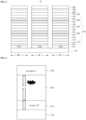
- FIG. 3 is a schematic cross-sectional view illustrating an OLED of an organic light emitting display device according to a first embodiment of the present disclosure.
- the OLED D1 includes an anode 210, a cathode 230 facing the anode 210 and an organic emitting layer 220 between the anode 210 and the cathode 230, and the organic emitting layer 220 includes a first emitting part 310 including a red EML 312, a second emitting part 320 including a green EML 322 and a third emitting part 330 including a blue EML 332.
- the OLED D1 has a three-stack structure.
- the organic emitting layer 220 may further include a first CGL 340 between the first and second emitting parts 310 and 320 and a second CGL 350 between the second and third emitting parts 320 and 330.
- the organic light emitting display device 100 includes red, green and blue pixel regions RP, GP and BP, and the OLED D1 is positioned in the red, green and blue pixel regions RP, GP and BP and emits white light.
- the anode 210 includes a first anode 210a in the blue pixel region BP, a second anode 210b in the green pixel region GP and a third anode 210c in the red pixel region RP, and each of the first to third anode 210a, 210b and 210c has the same thickness in a range of 500 to 600 ⁇ .
- the red EML 312 includes a red host and a red dopant.
- the red dopant may include one of a fluorescent compound, a phosphorescent compound and a delayed fluorescent compound.
- the red dopant may be a phosphorescent compound.
- the red EML 312 may have a thickness of 20 to 30nm.
- the red host may be selected from the group consisting of mCP-CN, CBP, mCBP, mCP, DPEPO, 2,8-bis(diphenylphosphoryl)dibenzothiophene (PPT), 1,3,5-tri[(3-pyridyl)-phen-3-yl]benzene (TmPyPB), 2,6-di(9H-carbazol-9-yl)pyridine (PYD-2Cz), 2,8-di(9H-carbazol-9-yl)dibenzothiophene (DCzDBT), 3',5'-di(carbazol-9-yl)-[1,1'-bipheyl]-3,5-dicarbonitrile (DCzTPA), 4 ⁇ -(9H-carbazol-9-yl)biphenyl-3,5-dicarbonitrile (pCzB-2CN), 3 ⁇ -(9H-carbazol-9-yl)biphenyl-3,5-d
- the red dopant may be selected from the group consisting of[bis(2-(4,6-dimethyl)phenylquinoline)](2,2,6,6-tetramethylheptane-3,5-dionate)iridium(III), bis[2-(4-n-hexylphenyl)quinoline](acetylacetonate)iridium(III) (Hex-Ir(phq)2(acac)), tris[2-(4-n-hexylphenyl)quinoline]iridium(III) (Hex-Ir(phq)3), tris[2-phenyl-4-methylquinoline]iridium(III) (Ir(Mphq)3), bis(2-phenylquinoline)(2,2,6,6-tetramethylheptene-3,5-dionate)iridium(III) (Ir(dpm)PQ2), bis(phenylisoquinoline)(2,2,6,6-tetramethylheptene
- the first emitting part 310 may further include at least one of a first hole transporting layer (HTL) 316 under the red EML 312 and a first electron transporting layer (ETL) 318 on the first EML 312.
- the first emitting part 310 may further include a hole injection layer (HIL) 314 under the first HTL 316.
- HTL hole transporting layer
- EML electron transporting layer
- HIL hole injection layer
- the first emitting part 310 may have a structure of the HIL 314, the first HTL 316, the red EML 312 and the first ETL 318 sequentially stacked on the anode 210.
- the HIL 314 may contact the anode 210.
- the second emitting part 320 is disposed over the first emitting part 310. Namely, the second emitting part 320 is positioned between the first emitting part 310 and the cathode 230.
- the green EML 322 includes a green host and a green dopant.
- the green dopant may include one of a fluorescent compound, a phosphorescent compound and a delayed fluorescent compound. In one embodiment of the present disclosure, the green dopant may be a phosphorescent compound.
- the green EML 322 may have a thickness of 30 to 40nm.
- the green host may be selected from the group consisting of mCP-CN, CBP, mCBP, mCP, DPEPO, 2,8-bis(diphenylphosphoryl)dibenzothiophene (PPT), TmPyPB, PYD-2Cz, 2,8-di(9H-carbazol-9-yl)dibenzothiophene (DCzDBT), 3',5'-di(carbazol-9-yl)-[1,1'-bipheyl]-3,5-dicarbonitrile (DCzTPA), 4 ⁇ -(9H-carbazol-9-yl)biphenyl-3,5-dicarbonitrile (pCzB-2CN), 3 ⁇ -(9H-carbazol-9-yl)biphenyl-3,5-dicarbonitrile (mCzB-2CN), TSPO1, and 9-(9-phenyl-9H-carbazol-6-yl)-9H-carbazole (
- the green dopant may be selected from the group consisting of bis(2-phenylpyridine)](pyridyl-2-benzofuro[2,3-b]pyridine)iridium), tris[2-phenylpyridine]iridium(III) (Ir(ppy)3), fac-tris(2-phenylpyridine)iridium(III) (fac-Ir(ppy)3), bis(2-phenylpyridine)(acetylacetonate)iridium(III) (Ir(ppy)2(acac)), tris[2-(p-tolyl)pyridine]iridium(III) (Ir(mppy)3), bis(2-(naphthalene-2-yl)pyridine)(acetylacetonate)iridium(III) (Ir(npy)2acac), tris(2-phenyl-3-methylpyridine)iidium (Ir(3mppy)3), and fac-tris(2-(3-p-xy
- the second emitting part 320 may further include at least one of a second HTL 324 under the green EML 322 and a second ETL 326 on the green EML 322.
- the second emitting part 320 may have a structure of the second HTL 324, the green EML 322 and the second ETL 326 sequentially stacked over the first emitting part 310.
- the third emitting part 330 is disposed over the second emitting part 320. Namely, the third emitting part 330 is positioned between the second emitting part 320 and the cathode 230.
- the blue EML 332 includes a blue host and a blue dopant.
- the blue dopant may include one of a fluorescent compound, a phosphorescent compound and a delayed fluorescent compound.
- the blue dopant may be a fluorescent compound.
- the blue EML 332 may have a thickness of 20 to 30nm.
- a thickness of the blue EML 332 may be substantially same as that of the red EML 312, and each of the thickness of each of the blue EML 332 and the red EML 312 may be smaller than that of the green EML 322.
- the blue host may be selected from the group consisting of 1,3-bis(carbazol-9-yl)benzene (mCP), 9-(3-(9H-carbazol-9-yl)phenyl)-9H-carbazole-3-carbonitrile (mCP-CN), 3,3'-bis(N-carbazolyl)-1,1'-biphenyl (mCBP), CBP-CN, 9-(3-(9H-Carbazol-9-yl)phenyl)-3-(diphenylphosphoryl)-9H-carbazole (mCPPO1) 3,5-Di(9H-carbazol-9-yl)biphenyl (Ph-mCP), TSPO1, 9-(3'-(9H-carbazol-9-yl)-[1,1'-biphenyl]-3-yl)-9H-pyrido[2,3-b]indole (CzBPCb), bis(2-methylphenyl)diphenyls
- the blue dopant may be selected from the group consisting of perylene, 4,4'-bis[4-(di-p-tolylamino)styryl]biphenyl (DPAVBi), 4-(di-p-tolylamino)-4,4' -[(di-p-tolylamino)styryl] stilbene (DPAVB), 4,4'-bis[4-(diphenylamino)styryl]biphenyl (BDAVBi), 2,7-bis(4-diphenylamino)styryl)-9,9-spiorfluorene (spiro-DPVBi), [1,4-bis[2-[4-[N,N-di(p-tolyl)amino]phenyl]vinyl] benzene (DSB), 1,4-di-[4-(N,N-diphenyl)amino]styryl-benzene (DSA), 2,5,8,11-te
- the third emitting part 330 may further include at least one of a third HTL 334 under the blue EML 332 and a third ETL 336 on the blue EML 332.
- the third emitting part 330 may further include an electron injection layer (EIL) 338 on the third ETL 336.
- EIL electron injection layer
- the third emitting part 330 may have a structure of the third HTL 334, the blue EML 332, the third ETL 336 and the EIL 338 sequentially stacked over the second emitting part 320.
- the EIL 338 may contact the cathode 230.
- the HIL 314 may include a hole injection material being at least one compound selected from the group consisting of 4,4',4"-tris(3-methylphenylamino)triphenylamine (MTDATA), 4,4',4"-tris(N,N-diphenyl-amino)triphenylamine (NATA), 4,4',4"-tris(N-(naphthalene-1-yl)-N-phenyl-amino)triphenylamine (1T-NATA), 4,4',4"-tris(N-(naphthalene-2-yl)-N-phenyl-amino)triphenylamine (2T-NATA), copper phthalocyanine(CuPc), tris(4-carbazoyl-9-yl-phenyl)amine (TCTA), N,N'-diphenyl-N,N'-bis(1-naphthyl)-1,1'-biphenyl-4,4"-diamine (NPB or N
- Each of the first to third HTLs 316, 324 and 334 may include a hole transporting material being at least one compound selected from the group consisting of N,N'-diphenyl-N,N'-bis(3-methylphenyl)-1,1'-biphenyl-4,4'-diamine (TPD), NPB (or NPD), 4,4'-bis(N-carbazolyl)-1,1'-biphenyl (CBP), poly[N,N'-bis(4-butylphenyl)-N,N'-bis(phenyl)-benzidine] (poly-TPD), (poly[(9,9-dioctylfluorenyl-2,7-diyl)-co-(4,4'-(N-(4-sec-butylphenyl)diphenylamine))] (TFB), di-[4-(N,N-di-p-tolyl-phenyl]cyclohe
- a thickness of the third HTL 334 may be greater than that of the first HTL 316 and smaller than that of the second HTL 324.
- the first HTL 316 may have a thickness of 25 to 35nm
- the second HTL 324 may have a thickness of 125 to 165nm
- the third HTL 334 may have a thickness of 45 to 85nm.
- Each of the first to third ETLs 318, 326 and 336 may include an electron transporting material being at least one compound selected from the group consisting of tris-(8-hydroxyquinoline aluminum (Alq 3 ), 2-biphenyl-4-yl-5-(4-t-butylphenyl)-1,3,4-oxadiazole (PBD), spiro-PBD, lithium quinolate (Liq), 1,3,5-tris(N-phenylbenzimidazol-2-yl)benzene (TPBi), bis(2-methyl-8-quinolinolato-N1,O8)-(1,1' -biphenyl-4-olato)aluminum (BAlq), 4,7-diphenyl-1,10-phenanthroline (Bphen), 2,9-bis(naphthalene-2-yl)-4,7-diphenyl-1,10-phenanthroline (NBphen), 2,9-dimethyl-4,7-diphenyl-1,10-
- PFNBr tris(phenylquinoxaline) (TPQ), diphenyl-4-triphenylsilyl-phenylphosphine oxide (TSPO1), and 2-[4-(9,10-di-2-naphthalen2-yl-2-anthracen-2-yl)phenyl]-1-phenyl-1H-benzimidazole (ZADN).
- a thickness of the first ETL 318 may be greater than that of the second ETL 326 and smaller than that of the third EML 336.
- the first ETL 318 may have a thickness of 20 to 30nm
- the second ETL 326 may have a thickness of 15 to 25nm
- the third ETL 336 may have a thickness of 25 to 35nm.
- the EIL 338 may include an electron injection material being at least one of LiF, CsF, NaF, BaF 2 , Liq, lithium benzoate and sodium stearate.
- the EIL 338 may have a thickness of 0.1 to 10nm.
- the first CGL 340 is positioned between the first and second emitting parts 310 and 320. Namely, the first and second emitting parts 310 and 320 are connected by the first CGL 340.
- the first CGL 340 may be a PN-junction layer of a first N-type CGL 342 and a first P-type CGL 344.
- the first N-type CGL 342 is positioned between the first ETL 318 and the second HTL 324, and the first P-type CGL 344 is positioned between the first N-type CGL 342 and the second HTL 324.
- the second CGL 350 is positioned between the second and third emitting parts 320 and 330. Namely, the second and third emitting parts 320 and 330 are connected by the second CGL 350.
- the second CGL 350 may be a PN-junction layer of a second N-type CGL 352 and a second P-type CGL 354.
- the second N-type CGL 352 is positioned between the second ETL 326 and the third HTL 334, and the second P-type CGL 354 is positioned between the second N-type CGL 352 and the third HTL 334.
- Each of the first and second N-type CGLs 342 and 352 may be an organic layer doped with an alkali metal, e.g., Li, Na, K and Cs, and/or an alkali earth metal, e.g., Mg, Sr, Ba and Ra.
- each of the first and second N-type CGLs 342 and 352 may be formed of an N-type charge generation material including a host being the organic material, e.g., 4,7-dipheny-1,10-phenanthroline (Bphen) and MTDATA, and a dopant being an alkali metal and/or an alkali earth metal, and the dopant may be doped with a weight % of 0.01 to 30.
- Each of the first and second N-type CGLs 342 and 352 may have a thickness of 10 to 25nm.
- a thickness of the first N-type CGL 342, e.g., 15 to 25nm) may be greater than that of the second N-type CGL 352, e.g., 10 to 20nm.
- Each of the first and second P-type CGLs 344 and 354 may be formed of a P-type charge generation material including an inorganic material, e.g., tungsten oxide (Wox), molybdenum oxide (MoOx), beryllium oxide (Be2O3) and vanadium oxide (V2O5), an organic material, e.g., NPD, HAT-CN, F4TCNQ, TPD, TNB, TCTA and N,N'-dioctyl-3,4,9,10-perylenedicarboximide (PTCDI-C8).
- Each of the first and second P-type CGLs 344 and 354 may have a thickness of 5 to 10nm.
- the organic emitting layer 220 between the anode 210 and the cathode 230 includes the first emitting part 310 including the red EML 312, the second emitting part 320 positioned between the first emitting part 310 and the cathode 230 and including the green EML 322, and the third emitting part 330 positioned between the second emitting part 320 and the cathode 230 and including the blue EML 332.
- the color uniformity of the OLED D1 is improved.
- the blue EML is positioned to be closer to the cathode being a reflective electrode so that the brightness (or luminance) of the blue light is slowly decreased than that of each of the red light and the green light according to a viewing angle. Accordingly, the luminance curves of the red, green and blue colors according to the viewing angle are not matched. In addition, since the OLED includes one blue EML, the luminance of the blue light is lowered and insufficient.
- the anode 210 has a thickness in a range of 500 to 600 ⁇ , the above problems can be prevented.
- the light from the blue EML 332 may be divided into a light reflected by the cathode 230 as the reflective electrode, a light reflected at an interface between the organic emitting layer 220 and the anode 210 as a transparent electrode, and a light reflected at an interface between the anode 210 and the planarization layer 150, the blue light efficiency at a front viewing angle is improved and a decreasing speed of the blue light luminance according to the viewing angle is increased when the constructive interference between the light reflected at an interface between the organic emitting layer 220 and the anode 210 and the light reflected at an interface between the anode 210 and the planarization layer 150 occurs.
- the emitting efficiency of the blue color is improved, and the luminance deviation in wavelength ranges according to a viewing angle is decreased.
- the anode 210 in the red, green and blue pixel regions RP, GP and BP has the same thickness in a range of 500 to 600 ⁇ , a cavity effect for the green color is not provided so that there is a problem of mismatching of the luminance curves in the blue color and the green color.
- FIG. 5 is a schematic cross-sectional view illustrating an OLED of an organic light emitting display device according to a second embodiment of the present disclosure.
- the OLED D2 includes an anode 210, a cathode 230 facing the anode 210 and an organic emitting layer 220 between the anode 210 and the cathode 230, and the organic emitting layer 220 includes a first emitting part 410 including a red EML 412, a second emitting part 420 including a green EML 422 and a third emitting part 430 including a blue EML 432.
- the OLED D2 has a three-stack structure.
- the organic emitting layer 220 may further include a first CGL 440 between the first and second emitting parts 410 and 420 and a second CGL 450 between the second and third emitting parts 420 and 430.
- the organic light emitting display device 100 includes red, green and blue pixel regions RP, GP and BP, and the OLED D2 is positioned in the red, green and blue pixel regions RP, GP and BP and emits white light.
- the anode 210 includes a first anode 210a in the blue pixel region BP, a second anode 210b in the green pixel region GP and a third anode 210c in the red pixel region RP, and the first to third anode 210a, 210b and 210c have a difference in a thickness.
- the first anode 210a has a first thickness t1
- the second anode 210b has a second thickness t2 being 2/5 to 2/3 of the first thickness t1.
- the second thickness t2 may be 1/2 of the first thickness t1.
- the first thickness t1 may be in a range of 500 to 600 ⁇
- the second thickness t2 may be in a range of 200 to 400 ⁇ .
- the first thickness t1 may be 600 ⁇
- the second thickness t2 may be 300 ⁇ .
- the third anode 210c may have a third thickness t3 being same as the first thickness t1 or the second thickness t2. But embodiments of the present disclosure are not limited thereto.
- the first thickness t1 of the first anode 210a in the blue pixel region BP can be greater than the second thickness t2 of the second anode 210b in the green pixel region GP, and in turn, the first thickness t1 of the first anode 210a in the blue pixel region BP can be greater than or equal to the third thickness t3 of the third anode 210a in the red pixel region RP. Accordingly, the third thickness t3 of the third anode 210 is not the thinnest of three anodes respectively in the blue, green and red pixel regions. Instead, the second thickness t2 of the second anode 210b in the green pixel region GP is the thinnest of the three anodes.
- the OLED D2 has high color gamut with 85% overlapping ratio in the color range standard BT 2020 and provide high emitting efficiency of green color.
- a first distance d1 from a lower surface of the cathode 230 to an upper surface of the anode 210 is in a range of 455 to 485nm
- a second distance d2 from the lower surface of the cathode 230 to a lower surface of the green EML 422 is in a range of 180 to 230nm.
- the first distance d1 from the cathode 230 to the anode 210 of the organic light emitting diode OLED D1 or OLED D2 can be approximately equal in each of the red pixel region RP, the green pixel region GP and the blue pixel region BP.
- a first travel distance of a blue light from the blue emitting material layer 432 to a distal surface (surface abutting the planarization layer 150, for example) of the anode 210a in the blue pixel region BP can be greater than a second travel distance of a blue light from the blue emitting material layer 432 to a distal surface of the anode 210b in the green pixel region GP.
- a third distance d3 from the lower surface of the cathode 230 to a lower surface of the blue EML 432 is in a range of 45 to 65nm
- a fourth distance d4 from the lower surface of the cathode 230 to a lower surface of the red EML 412 is in a range of 415 to 445nm.
- the red EML 412 includes a red host and a red dopant.
- the red dopant may include one of a fluorescent compound, a phosphorescent compound and a delayed fluorescent compound.
- the red dopant may be a phosphorescent compound.
- the red EML 412 may have a thickness of 20 to 30nm.
- the red host may be the above-mentioned red host material, and the red dopant may be the above-mentioned red dopant material.
- the first emitting part 410 may further include at least one of a first hole transporting layer (HTL) 416 under the red EML 412 and a first electron transporting layer (ETL) 418 on the first EML 412.
- the first emitting part 410 may further include a hole injection layer (HIL) 414 under the first HTL 416.
- HTL hole transporting layer
- EML electron transporting layer
- HIL hole injection layer
- the first emitting part 410 may have a structure of the HIL 414, the first HTL 416, the red EML 412 and the first ETL 418 sequentially stacked on the anode 210.
- the HIL 414 may contact the anode 210.
- the second emitting part 420 is disposed over the first emitting part 410. Namely, the second emitting part 420 is positioned between the first emitting part 410 and the cathode 230.
- the green EML 422 includes a green host and a green dopant.
- the green dopant may include one of a fluorescent compound, a phosphorescent compound and a delayed fluorescent compound. In one embodiment of the present disclosure, the green dopant may be a phosphorescent compound.
- the green EML 422 may have a thickness of 30 to 40nm.
- the green host may be the above-mentioned green host material, and the green dopant may be the above-mentioned green dopant material.
- the second emitting part 420 may further include at least one of a second HTL 424 under the green EML 422 and a second ETL 426 on the green EML 422.
- the second emitting part 420 may have a structure of the second HTL 424, the green EML 422 and the second ETL 426 sequentially stacked over the first emitting part 410.
- the third emitting part 430 is disposed over the second emitting part 420. Namely, the third emitting part 430 is positioned between the second emitting part 420 and the cathode 230.
- the blue EML 432 includes a blue host and a blue dopant.
- the blue dopant may include one of a fluorescent compound, a phosphorescent compound and a delayed fluorescent compound.
- the blue dopant may be a fluorescent compound.
- the blue EML 432 may have a thickness of 20 to 30nm.
- a thickness of the blue EML 432 may be substantially same as that of the red EML 412, and each of the thickness of each of the blue EML 432 and the red EML 412 may be smaller than that of the green EML 422.
- the blue host may be the above-mentioned blue host material, and the blue dopant may be the above-mentioned blue dopant material.
- the third emitting part 430 may further include at least one of a third HTL 434 under the blue EML 432 and a third ETL 436 on the blue EML 432.
- the third emitting part 430 may further include an electron injection layer (EIL) 438 on the third ETL 436.
- EIL electron injection layer
- the third emitting part 430 may have a structure of the third HTL 434, the blue EML 432, the third ETL 436 and the EIL 438 sequentially stacked over the second emitting part 420.
- the EIL 438 may contact the cathode 230.
- the HIL 414 may include the above-mentioned hole injection material and may have a thickness of 5 to 15nm
- Each of the first to third HTLs 416, 424 and 434 may include the above-mentioned hole transporting material.
- a thickness of the third HTL 434 may be greater than that of the first HTL 416 and smaller than that of the second HTL 424.
- the first HTL 416 may have a thickness of 25 to 35nm
- the second HTL 424 may have a thickness of 125 to 165nm
- the third HTL 434 may have a thickness of 45 to 85nm.
- Each of the first to third ETLs 418, 426 and 436 may include the above-mentioned electron transporting material.
- a thickness of the first ETL 418 may be greater than that of the second ETL 426 and smaller than that of the third ETL 436.
- the first ETL 418 may have a thickness of 20 to 30nm
- the second ETL 426 may have a thickness of 15 to 25nm
- the third ETL 436 may have a thickness of 25 to 35nm.
- the EIL 438 may include the above-mentioned electron injection material and may have a thickness of 0.1 to 10nm.
- the first CGL 440 is positioned between the first and second emitting parts 410 and 420. Namely, the first and second emitting parts 410 and 420 are connected by the first CGL 440.
- the first CGL 440 may be a PN-junction layer of a first N-type CGL 442 and a first P-type CGL 444.
- the first N-type CGL 442 is positioned between the first ETL 418 and the second HTL 424, and the first P-type CGL 444 is positioned between the first N-type CGL 442 and the second HTL 424.
- the second CGL 450 is positioned between the second and third emitting parts 420 and 430. Namely, the second and third emitting parts 420 and 430 are connected by the second CGL 450.
- the second CGL 450 may be a PN-junction layer of a second N-type CGL 452 and a second P-type CGL 454.
- the second N-type CGL 452 is positioned between the second ETL 426 and the third HTL 434, and the second P-type CGL 454 is positioned between the second N-type CGL 452 and the third HTL 434.
- Each of the first and second N-type CGLs 442 and 452 may include the above-mentioned N-type charge generation material and may have a thickness of 10 to 25nm. In one embodiment of the present disclosure, a thickness of the first N-type CGL 442, e.g., 15 to 25nm), may be greater than that of the second N-type CGL 452, e.g., 10 to 20nm.
- Each of the first and second P-type CGLs 444 and 454 may include the above-mentioned P-type charge generation material and may have a thickness of 5 to 10nm.
- the first anode 210a in the blue pixel region BP has a first thickness t1 in a range of 500 to 600 ⁇
- the second anode 210b in the green pixel region GP has a second thickness t2 being 2/5 to 2/3 of the first thickness t1.
- the OLED D2 has high color gamut with 85% overlapping ratio in the color range standard BT 2020 and provide high emitting efficiency of green color.
- the emitting efficiency of green color in the OLED D2 is further improved.
- the anodes in the red, green and blue pixel regions were formed with the same thickness (600 ⁇ ).
- the anodes in the red, green and blue pixel regions were formed with the same thickness (300 ⁇ ).
- the emission intensity in wavelength ranges of the OLED in Examples 1 and 2 are measured and shown in FIG. 6 .
- the luminance (emission intensity) of the blue color light is increased.
- the luminance (emission intensity) of the green color light is increased.
- the luminance of the red color light seems not to depend on a thickness of the anode and may be substantially constant.
- the anode in the green pixel region is formed with a thickness "T" of 600 ⁇ , 500 ⁇ , 400 ⁇ , 300 ⁇ , 200 ⁇ and 100 ⁇ .
- the emitting efficiency (cd/A), the color coordinate index (CIE) and the color gamut (CG) of the OLED in Example 3 are listed in Table 1.
- the color gamut is an overlapping % in the color range standard BT 2020.
- Table 1 T ( ⁇ ) R 600 600 600 600 600 600 G 600 500 400 300 200 100 B 600 600 600 600 600 cd/A R 20.9 20.9 20.9 20.9 20.9 G 41.5 45.4 48.3 49.8 49.6 47.5 B 2.5 2.5 2.5 2.5 2.5 2.5 2.5 2.5 2.5 2.5 2.5 2.5 2.5 2.5 2.5 2.5 2.5 2.5 2.5 2.5 2.5 W 112.7 112.7 112.7 112.7 112.7 112.7 CIE Rx 0.694 0.694 0.694 0.694 Ry 0.308 0.308 0.308 0.308 0.308 0.308 0.308 Gx 0.241 0.241 0.241 0.240 0.239 0.237 Gy 0.725 0.725 0.724 0.723 0.721 0.720 Bx 0.149 0.149 0.149 0.149 0.149 0.149 By 0.046 0.046 0.046
- the OLED has high emitting efficiency in the green color with desired color gamut and color coordinate index.
- the OLED D2 of the present disclosure when a first thickness t1 of the first anode 210a in the blue pixel region is 1/4 of a blue wavelength ( ⁇ B /n) in the anode and a second thickness t2 of the second anode 210b in the green pixel region is 2/5 to 2/3 of the first thickness t1, the luminance of the blue color and the luminance of the green color are increased.
- the luminance curves of the blue color and the green color according to viewing angles are matched so that the display quality of the organic light emitting display device 100 is improved.
- the second HTL was formed with a thickness of 185nm, and the third HTL was formed with a thickness of 25nm.
- the second HTL was formed with a thickness of 165nm, and the third HTL was formed with a thickness of 45nm.
- the second HTL was formed with a thickness of 145nm, and the third HTL was formed with a thickness of 65nm.
- the second HTL was formed with a thickness of 125nm, and the third HTL was formed with a thickness of 85nm.
- the second HTL was formed with a thickness of 105nm
- the third HTL was formed with a thickness of 105nm.
- the emitting efficiency (cd/A), the color coordinate index (CIE) and the color gamut (CG) of the OLED in Examples 4 to 8 are listed in Table 2.
- the color gamut is an overlapping % in the color range standard BT 2020.
- Table 2 Ex4 Ex5 Ex6 Ex7 Ex8 cd/A R 20.9 20.9 20.9 20.9 G 18.2 36.9 48.0 44.4 28.7 B 2.5 2.5 2.5 2.5 2.5 2.5 W 112.7 112.7 112.7 112.7 112.7 CIE Rx 0.694 0.694 0.694 0.694 Ry 0.308 0.308 0.308 0.308 0.308 Gx 0.191 0.218 0.236 0.253 0.274 Gy 0.743 0.736 0.726 0.714 0.694 Bx 0.149 0.149 0.149 0.149 0.149 By 0.046 0.046 0.046 0.046 0.046 0.046 0.046 0.046 CG BT2020 88.2 86.6 85.3 83.9 81.9
- the OLED has high green emitting efficiency with sufficient color gamut.
Landscapes
- Physics & Mathematics (AREA)
- Optics & Photonics (AREA)
- Engineering & Computer Science (AREA)
- Microelectronics & Electronic Packaging (AREA)
- General Physics & Mathematics (AREA)
- Theoretical Computer Science (AREA)
- Electroluminescent Light Sources (AREA)
Abstract
The present disclosure relates to an organic light emitting device comprising a substrate including red, green and blue pixel regions; and an organic light emitting diode including an anode, a cathode over the anode and an organic emitting layer between the anode and the cathode and corresponding to in the red, green and blue pixel regions, wherein the organic emitting layer includes a first emitting part including a red emitting material layer, a second emitting part including a green emitting material layer and positioned between the first emitting part and the cathode and a third emitting part including a blue emitting material layer and positioned between the second emitting part and the cathode, and wherein the anode in the blue pixel region has a first thickness, and the anode in the green pixel region has a second thickness being 2/5 to 2/3 of the first thickness.
Description
- The present application claims the benefit of
Korean Patent Application No. 10-2023-0011774 filed in the Republic of Korea on January 30, 2023 - The present disclosure relates to an organic light emitting device, and more specifically, to an organic light emitting device having high emitting efficiency and high color gamut (color reproductivity).
- As requests for a flat panel display device having a small occupied area have been increased, an organic light emitting display device including an OLED has been the subject of recent research and development.
- The OLED emits light by injecting electrons from a cathode as an electron injection electrode and holes from an anode as a hole injection electrode into an emitting material layer (EML), combining the electrons with the holes, generating an exciton, and transforming the exciton from an excited state to a ground state. A flexible substrate, for example, a plastic substrate, can be used as a base substrate where elements are formed. In addition, the organic light emitting display device can be operated at a voltage (e.g., 10V or below) lower than a voltage required to operate other display devices. Moreover, the organic light emitting display device has advantages in the power consumption and the color sense.
- Recently, a white OLED including a first emitting part, which includes a blue EML, a second emitting part, which includes a red EML and a green EML, and a third emitting part, which includes a blue EML, is introduced. However, in the white OLED, a color uniformity is degraded by the first and third emitting parts each including the blue EML.
- The present disclosure is directed to an organic light emitting device that substantially obviates one or more of the problems associated with the limitations and disadvantages of the related conventional art.
- Additional features and advantages of the present disclosure are set forth in the description which follows, and will be apparent from the description, or evident by practice of the present disclosure. The objectives and other advantages of the present disclosure are realized and attained by the features described herein as well as in the appended drawings.
- The object is solved by the features of the independent claims. Preferred embodiments are given in the dependent claims.
- To achieve these and other advantages in accordance with the purpose of the embodiments of the present disclosure, as described herein, an aspect of the present disclosure is an organic light emitting display device comprising a substrate including red, green and blue pixel regions; and an organic light emitting diode including an anode, a cathode over the anode and an organic emitting layer between the anode and the cathode and corresponding to in the red, green and blue pixel regions, wherein the organic emitting layer includes a first emitting part including a red emitting material layer, a second emitting part including a green emitting material layer and positioned between the first emitting part and the cathode and a third emitting part including a blue emitting material layer and positioned between the second emitting part and the cathode, and wherein the anode in the blue pixel region has a first thickness, and the anode in the green pixel region has a second thickness being 2/5 to 2/3 of the first thickness.
- In the following optional features are provided which can be combined with the above mentioned aspect alone or in combination or in sub combination.
- In one or more embodiments, the first thickness may be 1/4 of a blue wavelength in the anode, the blue wavelength in the anode means λB/n, wherein λB is a wavelength of the blue light, n is a refractive index of the anode.
- In one or more embodiments, the first thickness may be in a range of 500 to 600Å.
- In one or more embodiments, the second thickness may be in a range of 200 to 400Å.
- In one or more embodiments, a distance between a lower surface of the green emitting material layer and a lower surface of the cathode may be in a range of 180 to 230nm.
- In one or more embodiments, a distance between a lower surface of the blue emitting material layer and a lower surface of the cathode may be in a range of 45 to 65nm.
- In one or more embodiments, a distance between a lower surface of the red emitting material layer and a lower surface of the cathode may be in a range of 415 to 445nm.
- In one or more embodiments, the first emitting part may further include a first hole transporting layer under the red emitting material layer, a hole injection layer under the first hole transporting layer and a first electron transporting layer on the red emitting material layer.
- In one or more embodiments, the second emitting part may further include a second hole transporting layer under the green emitting material layer and a second electron transporting layer on the green emitting material layer.
- In one or more embodiments, the third emitting part may further include a third hole transporting layer under the blue emitting material layer, a third electron transporting layer on the blue emitting material layer and an electron injection layer on the third electron transporting layer.
- In one or more embodiments, a thickness of the third hole transporting layer may be greater than a thickness of the first hole transporting layer and/or may be smaller than a thickness of the second hole transporting layer.
- In one or more embodiments, the thickness of the second hole transporting layer may be in a range of 125 to 165nm.
- In one or more embodiments, the thickness of the third hole transporting layer may be in a range of 45 to 85nm.
- In one or more embodiments, the thickness of the first hole transporting layer may be in a range of 25 to 35nm.
- In one or more embodiments, the thickness of the second hole transporting layer may be in a range of 125 to 165nm.
- In one or more embodiments, the thickness of the third hole transporting layer may be in a range of 45 to 85nm.
- In one or more embodiments, a thickness of the first electron transporting layer may be greater than a thickness of the second electron transporting layer and/or may be smaller than a thickness of the third electron transporting layer.
- In one or more embodiments, the thickness of the first electron transporting layer may be a range of 20 to 30nm.
- In one or more embodiments, the thickness of the second electron transporting layer may be a range of 15 to 25nm.
- In one or more embodiments, the thickness of the third electron transporting layer may be a range of 25 to 35nm.
- In one or more embodiments, the anode in the red pixel region may have a third thickness being same as the first thickness or the second thickness.
- In one or more embodiments, the organic emitting layer further may include a first charge generation layer between the first and second emitting parts and a second charge generation layer between the second and third emitting parts.
- In one or more embodiments, the organic light emitting device may comprise a color filter layer corresponding to the red, green and blue pixel regions and positioned between the substrate and the organic light emitting diode.
- It is to be understood that both the foregoing general description and the following detailed description are exemplary and explanatory and are intended to further explain the present disclosure as claimed.
- The accompanying drawings, which are included to provide a further understanding of the present disclosure and are incorporated in and constitute a part of this specification, illustrate embodiments of the present disclosure and together with the description serve to explain the principles of the present disclosure.
-
FIG. 1 is a schematic circuit diagram illustrating an organic light emitting display device of the present disclosure. -
FIG. 2 is a schematic cross-sectional view illustrating an organic light emitting display device according to the present disclosure. -
FIG. 3 is a schematic cross-sectional view illustrating an OLED of an organic light emitting display device according to a first embodiment of the present disclosure. -
FIG. 4 schematic view illustrating a constructive interference of blue emission in the OLED of the display device of the first embodiment of the disclosure. -
FIG. 5 is a schematic cross-sectional view illustrating an OLED of an organic light emitting display device according to a second embodiment of the present disclosure. -
FIG.6 graph showing an emission intensity depending on the anode thickness in an OLED. - Reference will now be made in detail to aspects of the present disclosure, examples of which may be illustrated in the accompanying drawings. In the following description, when a detailed description of well-known functions or configurations related to this document is determined to unnecessarily cloud a gist of the inventive concept, the detailed description thereof will be omitted. The progression of processing steps and/or operations described is an example; however, the sequence of steps and/or operations is not limited to that set forth herein and may be changed as is known in the art, with the exception of steps and/or operations necessarily occurring in a particular order. Like reference numerals designate like elements throughout. Names of the respective elements used in the following explanations are selected only for convenience of writing the specification and may be thus different from those used in actual products.
- Advantages and features of the present disclosure and methods of achieving them will be apparent with reference to the aspects described below in detail with the accompanying drawings. However, the present disclosure is not limited to the aspects disclosed below, but can be realized in a variety of different forms, and only these aspects allow the disclosure of the present disclosure to be complete. The present disclosure is provided to fully inform the scope of the disclosure to the skilled in the art of the present disclosure.
- The shapes, sizes, proportions, angles, numbers, and the like disclosed in the drawings for explaining the aspects of the present disclosure are illustrative, and the present disclosure is not limited to the illustrated matters. The same reference numerals refer to the same elements throughout the specification. In addition, in describing the present disclosure, if it is determined that a detailed description of the related known technology unnecessarily obscure the subject matter of the present disclosure, the detailed description thereof can be omitted. When 'including', 'having', 'consisting', and the like are used in this specification, other parts may be added unless 'only' is used. When a component is expressed in the singular, cases including the plural are included unless specific statement is described.
- In construing an element, the element is construed as including an error or tolerance range although there is no explicit description of such an error or tolerance range.
- In describing a position relationship, for example, when a position relation between two parts is described as, for example, "on," "over," "under," and "next," one or more other parts may be disposed between the two parts unless a more limiting term, such as "just" or "direct(ly)" is used.
- In describing a time relationship, for example, when the temporal order is described as, for example, "after," "subsequent," "next," and "before," a case that is not continuous may be included unless a more limiting term, such as "just," "immediate(ly)," or "direct(ly)" is used.
- It will be understood that, although the terms "first," "second," etc. may be used herein to describe various elements, these elements should not be limited by these terms. These terms are only used to distinguish one element from another. For example, a first element could be termed a second element, and, similarly, a second element could be termed a first element, without departing from the scope of the present disclosure.
- Features of various aspects of the present disclosure may be partially or overall coupled to or combined with each other, and may be variously inter-operated with each other and driven technically as those skilled in the art can sufficiently understand. The aspects of the present disclosure may be carried out independently from each other, or may be carried out together in co-dependent relationship.
- Reference will now be made in detail to some of the examples and preferred embodiments, which are illustrated in the accompanying drawings.
- In the present disclosure, an organic light emitting device including the OLED may be an organic light emitting display device or an organic lightening device. As an example, an organic light emitting display device, which is a display device including the OLED of the present disclosure, will be mainly described.
-
FIG. 1 is a schematic circuit diagram illustrating an organic light emitting display device of the present disclosure. - As illustrated in
FIG. 1 , a gate line GL and a data line DL, which cross each other to define a pixel region (pixel) P, and a power line PL are formed in an organic light emitting display device. A switching thin film transistor (TFT) Ts, a driving TFT Td, a storage capacitor Cst and an OLED D are formed in the pixel region P. The pixel region P may include a red pixel region, a green pixel region and a blue pixel region. - The switching thin film transistor Ts is connected to the gate line GL and the data line DL, and the driving thin film transistor Td is connected between the switching thin film transistor Ts and the power line PL. The storage capacitor Cst is connected to a gate electrode and a drain electrode of the driving TFT Td, and the OLED D is connected to the driving thin film transistor Td.
- When the switching thin film transistor Ts is turned on by the gate signal applied through the gate line GL, the data signal applied through the data line DL is applied into a gate electrode of the driving thin film transistor Td and one electrode of the storage capacitor Cst through the switching thin film transistor Ts.
- The driving thin film transistor Td is turned on by the data signal applied into the gate electrode so that a current proportional to the data signal is supplied from the power line PL to the OLED D through the driving thin film transistor Td. The OLED D emits light having a luminance proportional to the current flowing through the driving thin film transistor Td.
- In this case, the storage capacitor Cst is charge with a voltage proportional to the data signal so that the voltage of the gate electrode in the driving thin film transistor Td is kept constant during one frame.
- Therefore, the organic light emitting display device can display a desired image.
-
FIG. 2 is a schematic cross-sectional view illustrating an organic light emitting display device according to the present disclosure. - As illustrated in
FIG. 2 , the organic light emittingdisplay device 100 includes asubstrate 110, where a red pixel region RP, a green pixel region GP and a blue pixel region BP are defined, a TFT Tr on thesubstrate 110, an OLED D, which is disposed over the TFT Tr and connected to the TFT Tr, and acolor filter layer 180 between thesubstrate 110 and the OLED D. - The
substrate 110 may be a glass substrate or a flexible substrate. For example, thesubstrate 110 may be a polyimide (PI) substrate, a polyethersulfone (PES) substrate, a polyethylenenaphthalate (PEN) substrate, a polyethylene terephthalate (PET) substrate or a polycarbonate (PC) substrate. - A
buffer layer 120 is formed on the substrate, and the TFT Tr, which respectively corresponds to the red, green and blue pixels RP, GP and BP, is formed on thebuffer layer 120. Thebuffer layer 120 may be omitted, and the TFT Tr may be positioned on thesubstrate 110. - A
semiconductor layer 122 is formed on thebuffer layer 120. Thesemiconductor layer 122 may include an oxide semiconductor material or polycrystalline silicon. When thesemiconductor layer 122 includes the oxide semiconductor material, a light-shielding pattern (not shown) may be formed under thesemiconductor layer 122. The light to thesemiconductor layer 122 is shielded or blocked by the light-shielding pattern such that thermal degradation of thesemiconductor layer 122 can be prevented. On the other hand, when thesemiconductor layer 122 includes polycrystalline silicon, impurities may be doped into both sides of thesemiconductor layer 122. - A
gate insulating layer 124 of an insulating material is formed on thesemiconductor layer 122 and over an entire surface of thesubstrate 110. Thegate insulating layer 124 may be formed of an inorganic insulating material such as silicon oxide (SiOx) or silicon nitride (SiNx). - A
gate electrode 130, which is formed of a conductive material, e.g., metal, is formed on thegate insulating layer 124 to correspond to a center of thesemiconductor layer 122. InFIG. 2 , thegate insulating layer 124 is formed on an entire surface of thesubstrate 110. Alternatively, thegate insulating layer 124 may be patterned to have the same shape as thegate electrode 130. - An interlayer insulating
layer 132, which is formed of an insulating material, is formed on thegate electrode 130 and over an entire surface of thesubstrate 110. The interlayer insulatinglayer 132 may be formed of an inorganic insulating material, e.g., silicon oxide or silicon nitride, or an organic insulating material, e.g., benzocyclobutene or photo-acryl. - The interlayer insulating
layer 132 includes first and second contact holes 134 and 136 exposing both sides of thesemiconductor layer 122. The first and second contact holes 134 and 136 are positioned at both sides of thegate electrode 130 to be spaced apart from thegate electrode 130. The first and second contact holes 134 and 136 are formed through the interlayer insulatinglayer 132 and thegate insulating layer 124. Alternatively, when thegate insulating layer 124 is patterned to have the same shape as thegate electrode 130, the first and second contact holes 134 and 136 is formed only through the interlayer insulatinglayer 132. - A
source electrode 140 and adrain electrode 142, which are formed of a conductive material, e.g., metal, are formed on theinterlayer insulating layer 132. Thesource electrode 140 and thedrain electrode 142 are spaced apart from each other with respect to thegate electrode 130 and respectively contact both sides of thesemiconductor layer 122 through the first and second contact holes 134 and 136. - The
semiconductor layer 122, thegate electrode 130, thesource electrode 140 and thedrain electrode 142 constitute the TFT Tr, and the TFT Tr may be an n-type. The TFT Tr serves as a driving element. Namely, the TFT Tr may correspond to the driving TFT Td (ofFIG. 1 ). - In the TFT Tr, the
gate electrode 130, thesource electrode 140, and thedrain electrode 142 are positioned over thesemiconductor layer 122. Namely, the TFT Tr has a coplanar structure. Alternatively, in the TFT Tr, the gate electrode may be positioned under the semiconductor layer, and the source and drain electrodes may be positioned over the semiconductor layer such that the TFT Tr may have an inverted staggered structure. In this instance, the semiconductor layer may include amorphous silicon. - The
color filter layer 180 is formed on theinterlayer insulating layer 132. Thecolor filter layer 180 includes red, green andblue color filters - The
red color filter 182 includes at least one of a red dye and a red pigment, thegreen color filter 184 includes at least one of a green dye and a green pigment, and theblue color filter 186 includes at least one of a blue dye and a blue pigment. - Although not shown, the gate line and the data line cross each other to define the pixel region, and the switching TFT is formed to be connected to the gate and data lines. The switching TFT is connected to the TFT Tr as the driving element. In addition, the power line, which may be formed to be parallel to and spaced apart from one of the gate and data lines, and the storage capacitor for maintaining the voltage of the gate electrode of the TFT Tr in one frame may be further formed.
- A
planarization layer 150 is formed on the TFT Tr and thecolor filter layer 180 and over an entire surface of thesubstrate 110. Theplanarization layer 150 has a flat top surface and includes adrain contact hole 152 exposing thedrain electrode 142 of the TFT Tr. - The OLED D is disposed on the
planarization layer 150 and includes ananode 210, which is connected to thedrain electrode 142 of the TFT Tr, an organic emittinglayer 220 on theanode 210 and acathode 230 on the organic emittinglayer 220. The OLED D is disposed at each of the red, green and blue pixel regions RP, GP and BP and emits white light in the red, green and blue pixel regions RP, GP and BP. - The
anode 210 is separately formed in each of the pixel regions RP, GP and BP. Theanode 210 may be formed of a transparent conductive oxide material having a relatively high work function. Theanode 210 may be a transparent electrode. For example, theanode 210 may include at least one of indium-tin-oxide (ITO), indium-zinc-oxide (IZO), indium-tin-zinc oxide (ITZO), tin oxide (SnO), zinc oxide (ZnO), indium-copper-oxide (ICO) and aluminum-zinc-oxide (Al:ZnO, AZO). - A
bank layer 166 is formed on theplanarization layer 150 to cover an edge of theanode 210. Namely, thebank layer 166 is positioned at a boundary of the pixel region and exposes a center of theanode 210 in the pixel region. - Since the OLED D emits blue light in each of the red, green and blue pixel regions RP, GP and BP, the organic emitting
layer 220 may be integrally formed as a common layer in the red, green and blue pixel regions RP, GP and BP without separation. Thebank layer 166 may be formed to prevent a current leakage at an edge of theanode 210 and may be omitted. - An organic emitting
layer 220 is formed on theanode 210. The organic emittinglayer 220 includes a first emitting part, which includes a red EML, a second emitting part, which includes a green EML, and a third emitting part, which includes a blue EML. In addition, the organic emittinglayer 220 may further include a first charge generation layer (CGL) between the first and second emitting parts and a second CGL between the second and third emitting parts. - The
cathode 230 is formed over thesubstrate 110 where the organic emittinglayer 220 is formed. Thecathode 230 covers an entire surface of the display area and may be formed of a conductive material having high reflectance. For example, thecathode 230 may be formed of a metallic material, such as aluminum (Al), magnesium (Mg), calcium (Ca), silver (Ag), their alloys or their combinations. - In the OLED D, the
anode 210 may be a transparent electrode, and thecathode 230 may be a reflective electrode. - As described below, in the blue pixel region BP, the
anode 210 has a pre-determined thickness so that the emitting efficiency in the blue pixel region is improved. - An encapsulation layer (or encapsulation film) is formed on the
cathode 230 to prevent penetration of moisture into the OLED D. The encapsulation film includes a first inorganic insulating layer, an organic insulating layer and a second inorganic insulating layer sequentially stacked, but it is not limited thereto. - In addition, a metal plate may be disposed on the encapsulation layer.
- The organic light emitting
display device 100 may further include a polarization plate for reducing an ambient light reflection. The polarization plate may be disposed under thesubstrate 110. For example, the polarization plate may be a circular polarization plate. - In
FIG. 2 , thecolor filter layer 180 is disposed between the OLED D and the interlayer insulatinglayer 132. However, a position of thecolor filter layer 180 is not limited between the OLED D and thesubstrate 110. - In addition, the organic light emitting
display device 100 may further include a color conversion layer between the OLED D and thecolor filter layer 180. The color conversion layer may include red, green and blue color conversion layers respectively corresponding to the red, green and blue pixel regions RP, GP and BP so that the white light from the OLED D can be converted into red, green and blue light. - As described above, the white light from the OLED passes through the red, green and
blue color filters - In
FIG. 2 , the OLED D emitting the white light is used for a display device. Alternatively, the OLED D may be formed on an entire surface of a substrate without at least one of the driving element and the color filter layer to be used for a lightening device. The display device and the lightening device each including the OLED D of the present disclosure may be referred to as an organic light emitting device. -
FIG. 3 is a schematic cross-sectional view illustrating an OLED of an organic light emitting display device according to a first embodiment of the present disclosure. - As shown in
FIG. 3 , the OLED D1 includes ananode 210, acathode 230 facing theanode 210 and an organic emittinglayer 220 between theanode 210 and thecathode 230, and the organic emittinglayer 220 includes a first emittingpart 310 including ared EML 312, a second emittingpart 320 including agreen EML 322 and a third emittingpart 330 including ablue EML 332. Namely, the OLED D1 has a three-stack structure. - The organic emitting
layer 220 may further include afirst CGL 340 between the first and second emittingparts second CGL 350 between the second and third emittingparts - The organic light emitting
display device 100 includes red, green and blue pixel regions RP, GP and BP, and the OLED D1 is positioned in the red, green and blue pixel regions RP, GP and BP and emits white light. - The
anode 210 includes afirst anode 210a in the blue pixel region BP, asecond anode 210b in the green pixel region GP and athird anode 210c in the red pixel region RP, and each of the first tothird anode - The
red EML 312 includes a red host and a red dopant. The red dopant may include one of a fluorescent compound, a phosphorescent compound and a delayed fluorescent compound. In one embodiment of the present disclosure, the red dopant may be a phosphorescent compound. Thered EML 312 may have a thickness of 20 to 30nm. - For example, the red host may be selected from the group consisting of mCP-CN, CBP, mCBP, mCP, DPEPO, 2,8-bis(diphenylphosphoryl)dibenzothiophene (PPT), 1,3,5-tri[(3-pyridyl)-phen-3-yl]benzene (TmPyPB), 2,6-di(9H-carbazol-9-yl)pyridine (PYD-2Cz), 2,8-di(9H-carbazol-9-yl)dibenzothiophene (DCzDBT), 3',5'-di(carbazol-9-yl)-[1,1'-bipheyl]-3,5-dicarbonitrile (DCzTPA), 4`-(9H-carbazol-9-yl)biphenyl-3,5-dicarbonitrile (pCzB-2CN), 3`-(9H-carbazol-9-yl)biphenyl-3,5-dicarbonitrile (mCzB-2CN), TSPO1, 9-(9-phenyl-9H-carbazol-6-yl)-9H-carbazole (CCP), 4-(3-(triphenylen-2-yl)phenyl)dibenzo[b,d]thiophene, 9-(4-(9H-carbazol-9-yl)phenyl)-9H-3,9'-bicarbazole, 9-(3-(9H-carbazol-9-yl)phenyl)-9H-3,9'-bicarbazole, 9-(6-(9H-carbazol-9-yl)pyridin-3-yl)-9H-3,9'-bicabazole, 9,9'-diphenyl-9H,9'H-3,3'-bicarbazole (BCzPh), 1,3,5-tris(carbazole-9-yl)benzene (TCP), TCTA, 4,4'-bis(carbazole-9-yl)-2,2'-dimethylbipheyl (CDBP), 2,7-bis(carbazole-9-yl)-9,9-dimethylfluorene (DMFL-CBP), 2,2',7,7'-tetrakis(carbazole-9-yl)-9,9-spiorofluorene (Spiro-CBP), and 3,6-bis(carbazole-9-yl)-9-(2-ethyl-hexyl)-9H-carbazole (TCz1).
- The red dopant may be selected from the group consisting of[bis(2-(4,6-dimethyl)phenylquinoline)](2,2,6,6-tetramethylheptane-3,5-dionate)iridium(III), bis[2-(4-n-hexylphenyl)quinoline](acetylacetonate)iridium(III) (Hex-Ir(phq)2(acac)), tris[2-(4-n-hexylphenyl)quinoline]iridium(III) (Hex-Ir(phq)3), tris[2-phenyl-4-methylquinoline]iridium(III) (Ir(Mphq)3), bis(2-phenylquinoline)(2,2,6,6-tetramethylheptene-3,5-dionate)iridium(III) (Ir(dpm)PQ2), bis(phenylisoquinoline)(2,2,6,6-tetramethylheptene-3,5-dionate)iridium(III) (Ir(dpm)(piq)2), bis[(4-n-hexylphenyl)isoquinoline](acetylacetonate)iridium(III) (Hex-Ir(piq)2(acac)), tris[2-(4-n-hexylphenyl)quinoline]iridium(III) (Hex-Ir(piq)3), tris(2-(3-methylphenyl)-7-methyl-quinolato)iridium (Ir(dmpq)3), bis[2-(2-methylphenyl)-7-methylquinoline](acetylacetonate)iridium(III) (Ir(dmpq)2(acac)), bis[2-(3,5-dimethylphenyl)-4-methyl-quinoline](acetylacetonate)iridium(III) (Ir(mphmq)2(acac)), and tris(dibenzoylmethane)mono(1,10-phenanthroline)europium(III) (Eu(dbm)3(phen)).
- The first emitting
part 310 may further include at least one of a first hole transporting layer (HTL) 316 under thered EML 312 and a first electron transporting layer (ETL) 318 on thefirst EML 312. In addition, the first emittingpart 310 may further include a hole injection layer (HIL) 314 under thefirst HTL 316. - For example, the first emitting
part 310 may have a structure of theHIL 314, thefirst HTL 316, thered EML 312 and thefirst ETL 318 sequentially stacked on theanode 210. In this configuration, theHIL 314 may contact theanode 210. - The second emitting
part 320 is disposed over the first emittingpart 310. Namely, the second emittingpart 320 is positioned between the first emittingpart 310 and thecathode 230. - The
green EML 322 includes a green host and a green dopant. The green dopant may include one of a fluorescent compound, a phosphorescent compound and a delayed fluorescent compound. In one embodiment of the present disclosure, the green dopant may be a phosphorescent compound. Thegreen EML 322 may have a thickness of 30 to 40nm. - For example, the green host may be selected from the group consisting of mCP-CN, CBP, mCBP, mCP, DPEPO, 2,8-bis(diphenylphosphoryl)dibenzothiophene (PPT), TmPyPB, PYD-2Cz, 2,8-di(9H-carbazol-9-yl)dibenzothiophene (DCzDBT), 3',5'-di(carbazol-9-yl)-[1,1'-bipheyl]-3,5-dicarbonitrile (DCzTPA), 4`-(9H-carbazol-9-yl)biphenyl-3,5-dicarbonitrile (pCzB-2CN), 3`-(9H-carbazol-9-yl)biphenyl-3,5-dicarbonitrile (mCzB-2CN), TSPO1, and 9-(9-phenyl-9H-carbazol-6-yl)-9H-carbazole (CCP).
- The green dopant may be selected from the group consisting of bis(2-phenylpyridine)](pyridyl-2-benzofuro[2,3-b]pyridine)iridium), tris[2-phenylpyridine]iridium(III) (Ir(ppy)3), fac-tris(2-phenylpyridine)iridium(III) (fac-Ir(ppy)3), bis(2-phenylpyridine)(acetylacetonate)iridium(III) (Ir(ppy)2(acac)), tris[2-(p-tolyl)pyridine]iridium(III) (Ir(mppy)3), bis(2-(naphthalene-2-yl)pyridine)(acetylacetonate)iridium(III) (Ir(npy)2acac), tris(2-phenyl-3-methylpyridine)iidium (Ir(3mppy)3), and fac-tris(2-(3-p-xylyl)phenyl)pyridine iridium(III) (TEG).
- The second emitting
part 320 may further include at least one of asecond HTL 324 under thegreen EML 322 and asecond ETL 326 on thegreen EML 322. - For example, the second emitting
part 320 may have a structure of thesecond HTL 324, thegreen EML 322 and thesecond ETL 326 sequentially stacked over the first emittingpart 310. - The third
emitting part 330 is disposed over the second emittingpart 320. Namely, the third emittingpart 330 is positioned between the second emittingpart 320 and thecathode 230. - The
blue EML 332 includes a blue host and a blue dopant. The blue dopant may include one of a fluorescent compound, a phosphorescent compound and a delayed fluorescent compound. In one embodiment of the present disclosure, the blue dopant may be a fluorescent compound. Theblue EML 332 may have a thickness of 20 to 30nm. For example, a thickness of theblue EML 332 may be substantially same as that of thered EML 312, and each of the thickness of each of theblue EML 332 and thered EML 312 may be smaller than that of thegreen EML 322. - For example, the blue host may be selected from the group consisting of 1,3-bis(carbazol-9-yl)benzene (mCP), 9-(3-(9H-carbazol-9-yl)phenyl)-9H-carbazole-3-carbonitrile (mCP-CN), 3,3'-bis(N-carbazolyl)-1,1'-biphenyl (mCBP), CBP-CN, 9-(3-(9H-Carbazol-9-yl)phenyl)-3-(diphenylphosphoryl)-9H-carbazole (mCPPO1) 3,5-Di(9H-carbazol-9-yl)biphenyl (Ph-mCP), TSPO1, 9-(3'-(9H-carbazol-9-yl)-[1,1'-biphenyl]-3-yl)-9H-pyrido[2,3-b]indole (CzBPCb), bis(2-methylphenyl)diphenylsilane (UGH-1), 1,4-bis(triphenylsilyl)benzene (UGH-2), 1,3-bis(triphenylsilyl)benzene (UGH-3), 9,9-spiorobifluoren-2-yl-diphenyl-phosphine oxide (SPPO1) and 9,9'-(5-(triphenylsilyl)-1,3-phenylene)bis(9H-carbazole) (SimCP).
- The blue dopant may be selected from the group consisting of perylene, 4,4'-bis[4-(di-p-tolylamino)styryl]biphenyl (DPAVBi), 4-(di-p-tolylamino)-4,4' -[(di-p-tolylamino)styryl] stilbene (DPAVB), 4,4'-bis[4-(diphenylamino)styryl]biphenyl (BDAVBi), 2,7-bis(4-diphenylamino)styryl)-9,9-spiorfluorene (spiro-DPVBi), [1,4-bis[2-[4-[N,N-di(p-tolyl)amino]phenyl]vinyl] benzene (DSB), 1,4-di-[4-(N,N-diphenyl)amino]styryl-benzene (DSA), 2,5,8,11-tetra-tetr-butylperylene (TBPe), bis(2-hydroxylphenyl)-pyridine)beryllium (Bepp2), 9-(9-Phenylcarbazole-3-yl)-10-(naphthalene-1-yl)anthracene (PCAN), mer-tris(1-phenyl-3-methylimidazolin-2-ylidene-C,C(2)'iridium(III) (mer-Ir(pmi)3), fac-Tris(1,3-diphenyl-benzimidazolin-2-ylidene-C,C(2)'iridium(III) (fac-Ir(dpbic)3), bis(3,4,5-trifluoro-2-(2-pyridyl)phenyl-(2-carboxypyridyl)iridium(III) (Ir(tfpd)2pic), tris(2-(4,6-difluorophenyl)pyridine))iridium(III) (Ir(Fppy)3) and bis[2-(4,6-difluorophenyl)pyridinato-C2,N](picolinato)iridium(III) (FIr-pic).
- The third
emitting part 330 may further include at least one of athird HTL 334 under theblue EML 332 and athird ETL 336 on theblue EML 332. In addition, the third emittingpart 330 may further include an electron injection layer (EIL) 338 on thethird ETL 336. - For example, the third emitting
part 330 may have a structure of thethird HTL 334, theblue EML 332, thethird ETL 336 and theEIL 338 sequentially stacked over the second emittingpart 320. In this configuration, theEIL 338 may contact thecathode 230. - The HIL 314 may include a hole injection material being at least one compound selected from the group consisting of 4,4',4"-tris(3-methylphenylamino)triphenylamine (MTDATA), 4,4',4"-tris(N,N-diphenyl-amino)triphenylamine (NATA), 4,4',4"-tris(N-(naphthalene-1-yl)-N-phenyl-amino)triphenylamine (1T-NATA), 4,4',4"-tris(N-(naphthalene-2-yl)-N-phenyl-amino)triphenylamine (2T-NATA), copper phthalocyanine(CuPc), tris(4-carbazoyl-9-yl-phenyl)amine (TCTA), N,N'-diphenyl-N,N'-bis(1-naphthyl)-1,1'-biphenyl-4,4"-diamine (NPB or NPD), 1,4,5,8,9,11-hexaazatriphenylenehexacarbonitrile(dipyrazino[2,3-f:2'3'-h]quinoxaline-2,3,6,7,10,11-hexacarbonitrile (HAT-CN), 1,3,5-tris[4-(diphenylamino)phenyl]benzene (TDAPB), poly(3,4-ethylenedioxythiphene)polystyrene sulfonate (PEDOT/PSS), N-(biphenyl-4-yl)-9,9-dimethyl-N-(4-(9-phenyl-9H-carbazol-3-yl)phenyl)-9H-fluoren-2-amine, and N,N'-diphenyl-N,N'-di[4-(N,N-diphenyl-amino)phenyl]benzidine (NPNPB). The
HIL 314 may have a thickness of 5 to 15nm - Each of the first to third HTLs 316, 324 and 334 may include a hole transporting material being at least one compound selected from the group consisting of N,N'-diphenyl-N,N'-bis(3-methylphenyl)-1,1'-biphenyl-4,4'-diamine (TPD), NPB (or NPD), 4,4'-bis(N-carbazolyl)-1,1'-biphenyl (CBP), poly[N,N'-bis(4-butylphenyl)-N,N'-bis(phenyl)-benzidine] (poly-TPD), (poly[(9,9-dioctylfluorenyl-2,7-diyl)-co-(4,4'-(N-(4-sec-butylphenyl)diphenylamine))] (TFB), di-[4-(N,N-di-p-tolyl-amino)-phenyl]cyclohexane (TAPC), 3,5-di(9H-carbazol-9-yl)-N,N-diphenylaniline (DCDPA), N-(biphenyl-4-yl)-9,9-dimethyl-N-(4-(9-phenyl-9H-carbazol-3-yl)phenyl)-9H-fluoren-2-amine, N-(biphenyl-4-yl)-N-(4-(9-phenyl-9H-carbazol-3-yl)phenyl)biphenyl-4-amine, and N-([1,1'- biphenyl]-4-yl)-9,9-dimethyl-N-(4-(9-phenl-9H-carbazol-3-yl)phenyl)-9H-fluoren-2-amine.
- A thickness of the
third HTL 334 may be greater than that of thefirst HTL 316 and smaller than that of thesecond HTL 324. For example, thefirst HTL 316 may have a thickness of 25 to 35nm, thesecond HTL 324 may have a thickness of 125 to 165nm, and thethird HTL 334 may have a thickness of 45 to 85nm. - Each of the first to third ETLs 318, 326 and 336 may include an electron transporting material being at least one compound selected from the group consisting of tris-(8-hydroxyquinoline aluminum (Alq3), 2-biphenyl-4-yl-5-(4-t-butylphenyl)-1,3,4-oxadiazole (PBD), spiro-PBD, lithium quinolate (Liq), 1,3,5-tris(N-phenylbenzimidazol-2-yl)benzene (TPBi), bis(2-methyl-8-quinolinolato-N1,O8)-(1,1' -biphenyl-4-olato)aluminum (BAlq), 4,7-diphenyl-1,10-phenanthroline (Bphen), 2,9-bis(naphthalene-2-yl)-4,7-diphenyl-1,10-phenanthroline (NBphen), 2,9-dimethyl-4,7-diphenyl-1,10-phenathroline (BCP), 3-(4-biphenyl)-4-phenyl-5-tert-butylphenyl-1,2,4-triazole (TAZ), 4-(naphthalen-1-yl)-3,5-diphenyl-4H-1,2,4-triazole (NTAZ), 1,3,5-tri(p-pyrid-3-yl-phenyl)benzene (TpPyPB), 2,4,6-tris(3'-(pyridin-3-yl)biphenyl-3-yl)1,3,5-triazine (TmPPPyTz), poly[9,9-bis(3'-((N,N-dimethyl)-N-ethylammonium)-propyl)-2,7-fluorene]-alt-2,7-(9,9-dioctylfluorene)]
- (PFNBr), tris(phenylquinoxaline) (TPQ), diphenyl-4-triphenylsilyl-phenylphosphine oxide (TSPO1), and 2-[4-(9,10-di-2-naphthalen2-yl-2-anthracen-2-yl)phenyl]-1-phenyl-1H-benzimidazole (ZADN).
- A thickness of the
first ETL 318 may be greater than that of thesecond ETL 326 and smaller than that of thethird EML 336. For example, thefirst ETL 318 may have a thickness of 20 to 30nm, thesecond ETL 326 may have a thickness of 15 to 25nm, and thethird ETL 336 may have a thickness of 25 to 35nm. - The
EIL 338 may include an electron injection material being at least one of LiF, CsF, NaF, BaF2, Liq, lithium benzoate and sodium stearate. TheEIL 338 may have a thickness of 0.1 to 10nm. - The
first CGL 340 is positioned between the first and second emittingparts parts first CGL 340. Thefirst CGL 340 may be a PN-junction layer of a first N-type CGL 342 and a first P-type CGL 344. - The first N-
type CGL 342 is positioned between thefirst ETL 318 and thesecond HTL 324, and the first P-type CGL 344 is positioned between the first N-type CGL 342 and thesecond HTL 324. - The
second CGL 350 is positioned between the second and third emittingparts parts second CGL 350. Thesecond CGL 350 may be a PN-junction layer of a second N-type CGL 352 and a second P-type CGL 354. - The second N-
type CGL 352 is positioned between thesecond ETL 326 and thethird HTL 334, and the second P-type CGL 354 is positioned between the second N-type CGL 352 and thethird HTL 334. - Each of the first and second N-
type CGLs type CGLs type CGLs type CGL 342, e.g., 15 to 25nm), may be greater than that of the second N-type CGL 352, e.g., 10 to 20nm. - Each of the first and second P-
type CGLs 344 and 354 may be formed of a P-type charge generation material including an inorganic material, e.g., tungsten oxide (Wox), molybdenum oxide (MoOx), beryllium oxide (Be2O3) and vanadium oxide (V2O5), an organic material, e.g., NPD, HAT-CN, F4TCNQ, TPD, TNB, TCTA and N,N'-dioctyl-3,4,9,10-perylenedicarboximide (PTCDI-C8). Each of the first and second P-type CGLs 344 and 354 may have a thickness of 5 to 10nm. - In the OLED D1 in the organic light emitting
display device 100 of the present disclosure, the organic emittinglayer 220 between theanode 210 and thecathode 230 includes the first emittingpart 310 including thered EML 312, the second emittingpart 320 positioned between the first emittingpart 310 and thecathode 230 and including thegreen EML 322, and the third emittingpart 330 positioned between the second emittingpart 320 and thecathode 230 and including theblue EML 332. As a result, the color uniformity of the OLED D1 is improved. - On the other hand, in the three-stack structure OLED including a first emitting part with a red EML, a second emitting part with a green EML and a third emitting part with a blue EML, the blue EML is positioned to be closer to the cathode being a reflective electrode so that the brightness (or luminance) of the blue light is slowly decreased than that of each of the red light and the green light according to a viewing angle. Accordingly, the luminance curves of the red, green and blue colors according to the viewing angle are not matched. In addition, since the OLED includes one blue EML, the luminance of the blue light is lowered and insufficient.
- However, in the OLED D1 of the present disclosure, the
anode 210 has a thickness in a range of 500 to 600Å, the above problems can be prevented. - Namely, referring to
FIG. 4 , which is a schematic view illustrating a constructive interference of blue emission in the OLED of the organic light emitting display device according to the first embodiment of the present disclosure, the light from theblue EML 332 may be divided into a light reflected by thecathode 230 as the reflective electrode, a light reflected at an interface between the organic emittinglayer 220 and theanode 210 as a transparent electrode, and a light reflected at an interface between theanode 210 and theplanarization layer 150, the blue light efficiency at a front viewing angle is improved and a decreasing speed of the blue light luminance according to the viewing angle is increased when the constructive interference between the light reflected at an interface between the organic emittinglayer 220 and theanode 210 and the light reflected at an interface between theanode 210 and theplanarization layer 150 occurs. - For this constructive interference, a thickness "T" of the
anode 210 should be 1/4 of a blue light wavelength (λB/n) in a medium (the anode), i.e., 500 to 600Å. (T=(λB/n)/4, λB=a wavelength of blue light, n=a refractive index of an anode) - Accordingly, in the organic light emitting
display device 100, the emitting efficiency of the blue color is improved, and the luminance deviation in wavelength ranges according to a viewing angle is decreased. - On the other hand, when the
anode 210 in the red, green and blue pixel regions RP, GP and BP has the same thickness in a range of 500 to 600Å, a cavity effect for the green color is not provided so that there is a problem of mismatching of the luminance curves in the blue color and the green color. -
FIG. 5 is a schematic cross-sectional view illustrating an OLED of an organic light emitting display device according to a second embodiment of the present disclosure. - As shown in
FIG. 5 , the OLED D2 includes ananode 210, acathode 230 facing theanode 210 and an organic emittinglayer 220 between theanode 210 and thecathode 230, and the organic emittinglayer 220 includes a first emittingpart 410 including ared EML 412, a second emittingpart 420 including agreen EML 422 and a third emittingpart 430 including ablue EML 432. Namely, the OLED D2 has a three-stack structure. - The organic emitting
layer 220 may further include afirst CGL 440 between the first and second emittingparts second CGL 450 between the second and third emittingparts - The organic light emitting
display device 100 includes red, green and blue pixel regions RP, GP and BP, and the OLED D2 is positioned in the red, green and blue pixel regions RP, GP and BP and emits white light. - The
anode 210 includes afirst anode 210a in the blue pixel region BP, asecond anode 210b in the green pixel region GP and athird anode 210c in the red pixel region RP, and the first tothird anode - Namely, the
first anode 210a has a first thickness t1, and thesecond anode 210b has a second thickness t2 being 2/5 to 2/3 of the first thickness t1. In one embodiment of the present disclosure, the second thickness t2 may be 1/2 of the first thickness t1. The first thickness t1 may be in a range of 500 to 600Å, and the second thickness t2 may be in a range of 200 to 400Å. In one embodiment of the present disclosure, the first thickness t1 may be 600Å, and the second thickness t2 may be 300Å. Thethird anode 210c may have a third thickness t3 being same as the first thickness t1 or the second thickness t2. But embodiments of the present disclosure are not limited thereto. In embodiments of the present disclosure, the first thickness t1 of thefirst anode 210a in the blue pixel region BP can be greater than the second thickness t2 of thesecond anode 210b in the green pixel region GP, and in turn, the first thickness t1 of thefirst anode 210a in the blue pixel region BP can be greater than or equal to the third thickness t3 of thethird anode 210a in the red pixel region RP. Accordingly, the third thickness t3 of thethird anode 210 is not the thinnest of three anodes respectively in the blue, green and red pixel regions. Instead, the second thickness t2 of thesecond anode 210b in the green pixel region GP is the thinnest of the three anodes. - As a result, the OLED D2 has high color gamut with 85% overlapping ratio in the color range standard BT 2020 and provide high emitting efficiency of green color.
- A first distance d1 from a lower surface of the
cathode 230 to an upper surface of theanode 210 is in a range of 455 to 485nm, and a second distance d2 from the lower surface of thecathode 230 to a lower surface of thegreen EML 422 is in a range of 180 to 230nm. As a result, the emitting efficiency of green color in the OLED D2 is improved. But embodiments of the present disclosure are not limited thereto. For example, the first distance d1 from thecathode 230 to theanode 210 of the organic light emitting diode OLED D1 or OLED D2 can be approximately equal in each of the red pixel region RP, the green pixel region GP and the blue pixel region BP. In this context, a first travel distance of a blue light from the blue emittingmaterial layer 432 to a distal surface (surface abutting theplanarization layer 150, for example) of theanode 210a in the blue pixel region BP can be greater than a second travel distance of a blue light from the blue emittingmaterial layer 432 to a distal surface of theanode 210b in the green pixel region GP. - A third distance d3 from the lower surface of the
cathode 230 to a lower surface of theblue EML 432 is in a range of 45 to 65nm, and a fourth distance d4 from the lower surface of thecathode 230 to a lower surface of thered EML 412 is in a range of 415 to 445nm. - The
red EML 412 includes a red host and a red dopant. The red dopant may include one of a fluorescent compound, a phosphorescent compound and a delayed fluorescent compound. In one embodiment of the present disclosure, the red dopant may be a phosphorescent compound. Thered EML 412 may have a thickness of 20 to 30nm. - The red host may be the above-mentioned red host material, and the red dopant may be the above-mentioned red dopant material.
- The first emitting
part 410 may further include at least one of a first hole transporting layer (HTL) 416 under thered EML 412 and a first electron transporting layer (ETL) 418 on thefirst EML 412. In addition, the first emittingpart 410 may further include a hole injection layer (HIL) 414 under thefirst HTL 416. - For example, the first emitting
part 410 may have a structure of theHIL 414, thefirst HTL 416, thered EML 412 and thefirst ETL 418 sequentially stacked on theanode 210. In this configuration, theHIL 414 may contact theanode 210. - The second emitting
part 420 is disposed over the first emittingpart 410. Namely, the second emittingpart 420 is positioned between the first emittingpart 410 and thecathode 230. - The
green EML 422 includes a green host and a green dopant. The green dopant may include one of a fluorescent compound, a phosphorescent compound and a delayed fluorescent compound. In one embodiment of the present disclosure, the green dopant may be a phosphorescent compound. Thegreen EML 422 may have a thickness of 30 to 40nm. - The green host may be the above-mentioned green host material, and the green dopant may be the above-mentioned green dopant material.
- The second emitting
part 420 may further include at least one of asecond HTL 424 under thegreen EML 422 and asecond ETL 426 on thegreen EML 422. - For example, the second emitting
part 420 may have a structure of thesecond HTL 424, thegreen EML 422 and thesecond ETL 426 sequentially stacked over the first emittingpart 410. - The third
emitting part 430 is disposed over the second emittingpart 420. Namely, the third emittingpart 430 is positioned between the second emittingpart 420 and thecathode 230. - The
blue EML 432 includes a blue host and a blue dopant. The blue dopant may include one of a fluorescent compound, a phosphorescent compound and a delayed fluorescent compound. In one embodiment of the present disclosure, the blue dopant may be a fluorescent compound. Theblue EML 432 may have a thickness of 20 to 30nm. For example, a thickness of theblue EML 432 may be substantially same as that of thered EML 412, and each of the thickness of each of theblue EML 432 and thered EML 412 may be smaller than that of thegreen EML 422. - The blue host may be the above-mentioned blue host material, and the blue dopant may be the above-mentioned blue dopant material.
- The third
emitting part 430 may further include at least one of athird HTL 434 under theblue EML 432 and athird ETL 436 on theblue EML 432. In addition, the third emittingpart 430 may further include an electron injection layer (EIL) 438 on thethird ETL 436. - For example, the third emitting
part 430 may have a structure of thethird HTL 434, theblue EML 432, thethird ETL 436 and the EIL 438 sequentially stacked over the second emittingpart 420. In this configuration, the EIL 438 may contact thecathode 230. - The
HIL 414 may include the above-mentioned hole injection material and may have a thickness of 5 to 15nm - Each of the first to
third HTLs third HTL 434 may be greater than that of thefirst HTL 416 and smaller than that of thesecond HTL 424. For example, thefirst HTL 416 may have a thickness of 25 to 35nm, thesecond HTL 424 may have a thickness of 125 to 165nm, and thethird HTL 434 may have a thickness of 45 to 85nm. - Each of the first to
third ETLs first ETL 418 may be greater than that of thesecond ETL 426 and smaller than that of thethird ETL 436. For example, thefirst ETL 418 may have a thickness of 20 to 30nm, thesecond ETL 426 may have a thickness of 15 to 25nm, and thethird ETL 436 may have a thickness of 25 to 35nm. - The EIL 438 may include the above-mentioned electron injection material and may have a thickness of 0.1 to 10nm.
- The
first CGL 440 is positioned between the first and second emittingparts parts first CGL 440. Thefirst CGL 440 may be a PN-junction layer of a first N-type CGL 442 and a first P-type CGL 444. - The first N-
type CGL 442 is positioned between thefirst ETL 418 and thesecond HTL 424, and the first P-type CGL 444 is positioned between the first N-type CGL 442 and thesecond HTL 424. - The
second CGL 450 is positioned between the second and third emittingparts parts second CGL 450. Thesecond CGL 450 may be a PN-junction layer of a second N-type CGL 452 and a second P-type CGL 454. - The second N-
type CGL 452 is positioned between thesecond ETL 426 and thethird HTL 434, and the second P-type CGL 454 is positioned between the second N-type CGL 452 and thethird HTL 434. - Each of the first and second N-
type CGLs type CGL 442, e.g., 15 to 25nm), may be greater than that of the second N-type CGL 452, e.g., 10 to 20nm. - Each of the first and second P-
type CGLs - In the OLED D2 in the organic light emitting
display device 100 of the present disclosure, thefirst anode 210a in the blue pixel region BP has a first thickness t1 in a range of 500 to 600Å, and thesecond anode 210b in the green pixel region GP has a second thickness t2 being 2/5 to 2/3 of the first thickness t1. As result, the OLED D2 has high color gamut with 85% overlapping ratio in the color range standard BT 2020 and provide high emitting efficiency of green color. - In addition, since the lower surface of the
green EML 422 is spaced apart from a lower surface of thecathode 230 by the second distance d2, i.e., 180 to 230nm, the emitting efficiency of green color in the OLED D2 is further improved. - An anode (ITO), an HIL (10nm), a first HTL (30nm), a red EML (25nm), a first ETL (25nm), a first N-type CGL (20nm), a first P-type CGL (10nm), a second HTL (145nm), a green EML (40nm), a second ETL (20nm), a second N-type CGL (15nm), a second P-type CGL (10nm), a third HTL (65nm), a blue EML (25nm), a third ETL (30nm), an EIL (1nm), and a cathode (Al, 50nm) were sequentially stacked to form a white OLED.
- The anodes in the red, green and blue pixel regions were formed with the same thickness (600Å).
- The anodes in the red, green and blue pixel regions were formed with the same thickness (300Å).
- The emission intensity in wavelength ranges of the OLED in Examples 1 and 2 are measured and shown in
FIG. 6 . - As shown in
FIG. 6 , in the OLED with the anode having a thickness of 600Å, the luminance (emission intensity) of the blue color light is increased. On the other hand, in the OLED with the anode having a thickness of 300Å, the luminance (emission intensity) of the green color light is increased. The luminance of the red color light seems not to depend on a thickness of the anode and may be substantially constant. - In the OLED of Example 1, the anode in the green pixel region is formed with a thickness "T" of 600Å, 500Å, 400Å, 300Å, 200Å and 100Å.
- The emitting efficiency (cd/A), the color coordinate index (CIE) and the color gamut (CG) of the OLED in Example 3 are listed in Table 1. The color gamut is an overlapping % in the color range standard BT 2020.
Table 1 T (Å) R 600 600 600 600 600 600 G 600 500 400 300 200 100 B 600 600 600 600 600 600 cd/A R 20.9 20.9 20.9 20.9 20.9 20.9 G 41.5 45.4 48.3 49.8 49.6 47.5 B 2.5 2.5 2.5 2.5 2.5 2.5 W 112.7 112.7 112.7 112.7 112.7 112.7 CIE Rx 0.694 0.694 0.694 0.694 0.694 0.694 Ry 0.308 0.308 0.308 0.308 0.308 0.308 Gx 0.241 0.241 0.241 0.240 0.239 0.237 Gy 0.725 0.725 0.724 0.723 0.721 0.720 Bx 0.149 0.149 0.149 0.149 0.149 0.149 By 0.046 0.046 0.046 0.046 0.046 0.046 CG BT2020 85.0 85.0 85.0 85.0 85.0 85.0 - As shown in Table 1, in the OLED with the anode in the green pixel with a thickness of 200 to 400Å, the OLED has high emitting efficiency in the green color with desired color gamut and color coordinate index.
- Namely, as the OLED D2 of the present disclosure, when a first thickness t1 of the
first anode 210a in the blue pixel region is 1/4 of a blue wavelength (λB/n) in the anode and a second thickness t2 of thesecond anode 210b in the green pixel region is 2/5 to 2/3 of the first thickness t1, the luminance of the blue color and the luminance of the green color are increased. - In addition, the luminance curves of the blue color and the green color according to viewing angles are matched so that the display quality of the organic light emitting
display device 100 is improved. - After a first anode (ITO, 600Å), a second anode (ITO, 300Å) and a third anode (ITO, 600Å) were formed in the blue, green and red pixel regions, respectively, an HIL (10nm), a first HTL (30nm), a red EML (25nm), a first ETL (25nm), a first N-type CGL (20nm), a first P-type CGL (10nm), a second HTL, a green EML (40nm), a second ETL (20nm), a second N-type CGL (15nm), a second P-type CGL (10nm), a third HTL, a blue EML (25nm), a third ETL (30nm), an EIL (1nm), and a cathode (Al, 50nm) were sequentially stacked on the first to third anodes to form a white OLED.
- The second HTL was formed with a thickness of 185nm, and the third HTL was formed with a thickness of 25nm.
- The second HTL was formed with a thickness of 165nm, and the third HTL was formed with a thickness of 45nm.
- The second HTL was formed with a thickness of 145nm, and the third HTL was formed with a thickness of 65nm.
- The second HTL was formed with a thickness of 125nm, and the third HTL was formed with a thickness of 85nm.
- The second HTL was formed with a thickness of 105nm, and the third HTL was formed with a thickness of 105nm.
- The emitting efficiency (cd/A), the color coordinate index (CIE) and the color gamut (CG) of the OLED in Examples 4 to 8 are listed in Table 2. The color gamut is an overlapping % in the color range standard BT 2020.
Table 2 Ex4 Ex5 Ex6 Ex7 Ex8 cd/A R 20.9 20.9 20.9 20.9 20.9 G 18.2 36.9 48.0 44.4 28.7 B 2.5 2.5 2.5 2.5 2.5 W 112.7 112.7 112.7 112.7 112.7 CIE Rx 0.694 0.694 0.694 0.694 0.694 Ry 0.308 0.308 0.308 0.308 0.308 Gx 0.191 0.218 0.236 0.253 0.274 Gy 0.743 0.736 0.726 0.714 0.694 Bx 0.149 0.149 0.149 0.149 0.149 By 0.046 0.046 0.046 0.046 0.046 CG BT2020 88.2 86.6 85.3 83.9 81.9 - As shown in Table 2, in the OLED of Examples 5 to 7, in which a lower surface of the green EML is spaced apart from the cathode as a reflective electrode by a distance of 180 to 230nm, the OLED has high green emitting efficiency with sufficient color gamut.
- It will be apparent to those skilled in the art that various modifications and variations can be made in the embodiments of the present disclosure without departing from the scope of the present disclosure. Thus, it is intended that the modifications and variations cover this disclosure provided they come within the scope of the appended claims and their equivalents.
Claims (15)
- An organic light emitting device, comprising:a substrate (110) including red, green and blue pixel regions (RP, GP, BP); andan organic light emitting diode (D) including an anode (210), a cathode (230) over the anode (210) and an organic emitting layer (220) between the anode (210) and the cathode (230) and corresponding to in the red, green and blue pixel regions (RP, GP, BP),wherein the organic emitting layer (220) includes a first emitting part (310) including a red emitting material layer (312), a second emitting part (320) including a green emitting material layer (322) and positioned between the first emitting part (310) and the cathode (230) and a third emitting part (330) including a blue emitting material layer (332) and positioned between the second emitting part (320) and the cathode (230), andwherein the anode (210a) in the blue pixel region (BP) has a first thickness (t1), and the anode (210b) in the green pixel region (GP) has a second thickness (t2) being 2/5 to 2/3 of the first thickness (11).
- The organic light emitting device according to claim 1, wherein the first thickness (t1) is 1/4 of a blue wavelength in the anode (210) wherein the blue wavelength in the anode means λB/n, wherein λB is a wavelength of the blue light, n is a refractive index of the anode (210).
- The organic light emitting device according to claim 1 or 2, wherein the first thickness (T1) is in a range of 500 to 600Å.
- The organic light emitting device according to any one of the claims 1, 2 or 3, wherein the second thickness (t2) is in a range of 200 to 400Å.
- The organic light emitting device according to any one of the preceding claims, wherein a distance between a lower surface of the green emitting material layer (322) and a lower surface of the cathode (230) is in a range of 180 to 230nm.
- The organic light emitting device according to any one of the preceding claims, wherein a distance between a lower surface of the blue emitting material layer (332) and a lower surface of the cathode (230) is in a range of 45 to 65nm, and a distance between a lower surface of the red emitting material layer (312) and a lower surface of the cathode (230) is in a range of 415 to 445nm.
- The organic light emitting device according to any one of the preceding claims"wherein the first emitting part (310) further includes a first hole transporting layer (316) under the red emitting material layer, a hole injection layer (314) under the first hole transporting layer (316) and a first electron transporting layer (318) on the red emitting material layer (312),wherein the second emitting part (320) further includes a second hole transporting layer (324) under the green emitting material layer (322) and a second electron transporting layer (326) on the green emitting material layer (322), andwherein the third emitting part (330) further includes a third hole transporting layer (334) under the blue emitting material layer (332), a third electron transporting layer (336) on the blue emitting material layer (332) and an electron injection layer (338) on the third electron transporting layer (336).
- The organic light emitting device according to claim 7, wherein a thickness of the third hole transporting layer (334) is greater than a thickness of the first hole transporting layer (314) and is smaller than a thickness of the second hole transporting layer (324).
- The organic light emitting device according to claim 7 or 8, wherein the thickness of the second hole transporting layer (324) is in a range of 125 to 165nm, and the thickness of the third hole transporting layer (334) is in a range of 45 to 85nm.
- The organic light emitting device according to any one of the claims 7, 8 or 9, wherein the thickness of the first hole transporting layer (314) is in a range of 25 to 35nm, the thickness of the second hole transporting layer (324) is in a range of 125 to 165nm, and the thickness of the third hole transporting layer (343)is in a range of 45 to 85nm.
- The organic light emitting device according to any one of the claims 7-10, wherein a thickness of the first electron transporting layer (316) is greater than a thickness of the second electron transporting layer (326) and is smaller than a thickness of the third electron transporting layer (336).
- The organic light emitting device according to any one of the claims 7-11, wherein the thickness of the first electron transporting layer (316) is a range of 20 to 30nm, the thickness of the second electron transporting layer (326) is a range of 15 to 25nm, and the thickness of the third electron transporting layer (336) is a range of 25 to 35nm.
- The organic light emitting device according to any one of the preceding claims, wherein the anode (210c) in the red pixel region (RP) has a third thickness (t3) being same as the first thickness (t1) or the second thickness (t2).
- The organic light emitting device according to any one of the preceding claims, wherein the organic emitting layer (220) further includes a first charge generation layer (340) between the first and second emitting parts (310, 320) and a second charge generation layer (350) between the second and third emitting parts (320, 330).
- The organic light emitting device according to any one of the preceding claims, further comprising a color filter layer (180) corresponding to the red, green and blue pixel regions (RP, GP, BP) and positioned between the substrate (110) and the organic light emitting diode (D).
Applications Claiming Priority (1)
| Application Number | Priority Date | Filing Date | Title |
|---|---|---|---|
| KR1020230011774A KR20240119557A (en) | 2023-01-30 | 2023-01-30 | Organic light emitting device |
Publications (1)
| Publication Number | Publication Date |
|---|---|
| EP4408138A1 true EP4408138A1 (en) | 2024-07-31 |
Family
ID=89426961
Family Applications (1)
| Application Number | Title | Priority Date | Filing Date |
|---|---|---|---|
| EP23220557.5A Pending EP4408138A1 (en) | 2023-01-30 | 2023-12-28 | Organic light emitting device |
Country Status (4)
| Country | Link |
|---|---|
| US (1) | US20240260296A1 (en) |
| EP (1) | EP4408138A1 (en) |
| KR (1) | KR20240119557A (en) |
| CN (1) | CN118414052A (en) |
Citations (4)
| Publication number | Priority date | Publication date | Assignee | Title |
|---|---|---|---|---|
| US20110073885A1 (en) * | 2009-09-25 | 2011-03-31 | Chang-Oh Kim | Organic electroluminescent device |
| US20150014661A1 (en) * | 2013-07-09 | 2015-01-15 | Samsung Display Co., Ltd. | Organic light emitting display device and method of manufacturing an organic light emitting display device |
| KR20180078641A (en) * | 2016-12-30 | 2018-07-10 | 엘지디스플레이 주식회사 | Organic Light Emitting Device and Organic Light Emitting Display Apparatus using the same |
| KR20230011774A (en) | 2021-07-14 | 2023-01-25 | 현대모비스 주식회사 | Method and system for data recording of vehicle |
Family Cites Families (5)
| Publication number | Priority date | Publication date | Assignee | Title |
|---|---|---|---|---|
| JP5919807B2 (en) * | 2011-03-30 | 2016-05-18 | ソニー株式会社 | ORGANIC LIGHT EMITTING ELEMENT, METHOD FOR MANUFACTURING ORGANIC LIGHT EMITTING ELEMENT, AND DISPLAY DEVICE |
| CN109103214B (en) * | 2017-06-20 | 2020-11-06 | 京东方科技集团股份有限公司 | Organic light emitting diode display panel, method for making the same, and display device |
| CN110610975B (en) * | 2019-09-23 | 2022-04-08 | 京东方科技集团股份有限公司 | Display substrate and preparation method thereof, and display device |
| US11031577B1 (en) * | 2019-11-26 | 2021-06-08 | OLEDWorks LLC | Multimodal microcavity OLED with multiple blue emitting layers |
| US12274161B2 (en) * | 2020-05-29 | 2025-04-08 | Lg Display Co., Ltd. | Organic light emitting device |
-
2023
- 2023-01-30 KR KR1020230011774A patent/KR20240119557A/en active Pending
- 2023-11-29 CN CN202311609526.5A patent/CN118414052A/en active Pending
- 2023-12-08 US US18/533,912 patent/US20240260296A1/en active Pending
- 2023-12-28 EP EP23220557.5A patent/EP4408138A1/en active Pending
Patent Citations (4)
| Publication number | Priority date | Publication date | Assignee | Title |
|---|---|---|---|---|
| US20110073885A1 (en) * | 2009-09-25 | 2011-03-31 | Chang-Oh Kim | Organic electroluminescent device |
| US20150014661A1 (en) * | 2013-07-09 | 2015-01-15 | Samsung Display Co., Ltd. | Organic light emitting display device and method of manufacturing an organic light emitting display device |
| KR20180078641A (en) * | 2016-12-30 | 2018-07-10 | 엘지디스플레이 주식회사 | Organic Light Emitting Device and Organic Light Emitting Display Apparatus using the same |
| KR20230011774A (en) | 2021-07-14 | 2023-01-25 | 현대모비스 주식회사 | Method and system for data recording of vehicle |
Also Published As
| Publication number | Publication date |
|---|---|
| CN118414052A (en) | 2024-07-30 |
| US20240260296A1 (en) | 2024-08-01 |
| KR20240119557A (en) | 2024-08-06 |
Similar Documents
| Publication | Publication Date | Title |
|---|---|---|
| KR102477262B1 (en) | Organic electroluminescence display device | |
| KR102421769B1 (en) | Organic light emitting diode and organic light emitting display device including the same | |
| KR102455727B1 (en) | Organic light emitting diode and organic light emitting display device including the same | |
| KR20170049702A (en) | Organic electroluminescent device and display device including the same | |
| KR102353804B1 (en) | Organic light emitting device | |
| KR102715632B1 (en) | Organic electroluminescence display device | |
| KR20180078641A (en) | Organic Light Emitting Device and Organic Light Emitting Display Apparatus using the same | |
| US20160276601A1 (en) | Organic light emitting device and display device having the same | |
| KR20240120636A (en) | Organic light emitting diode and organic light emitting device including the same | |
| KR102322768B1 (en) | Organic light-emitting display apparatus and flat display including the same | |
| US20240206214A1 (en) | Organic light emitting diode and organic light emitting device | |
| US20240244857A1 (en) | Organic compound, organic light emitting diode and organic light emitting device having the compound | |
| US20240260296A1 (en) | Organic light emitting device | |
| CN114512619B (en) | Organic light emitting diode and organic light emitting device including the same | |
| KR20240068175A (en) | Organic light emitting diode and organic light emitting device having thereof | |
| US20240276762A1 (en) | Organic light emitting diode and organic light emitting device including the same | |
| US20240276754A1 (en) | Organic light emitting device | |
| US12615910B2 (en) | Organic light emitting diode and organic light emitting device | |
| US20240244967A1 (en) | Organic Light Emitting Diode and Organic Light Emitting Device Including the Same | |
| US20240237525A1 (en) | Organic Light Emitting Diode and Organic Light Emitting Device Including the Same | |
| US20240244871A1 (en) | Organic light emitting diode and organic light emitting device including the same | |
| EP4395515B1 (en) | Organic light emitting diode and organic light emitting device including the same | |
| US20240237377A1 (en) | Organic light emitting diode and organic light emitting display device including the same | |
| US20240244971A1 (en) | Organic light emitting diode and organic light emitting device including the same | |
| EP4199686A1 (en) | Organic light emitting diode and organic light emitting device including the same |
Legal Events
| Date | Code | Title | Description |
|---|---|---|---|
| PUAI | Public reference made under article 153(3) epc to a published international application that has entered the european phase |
Free format text: ORIGINAL CODE: 0009012 |
|
| STAA | Information on the status of an ep patent application or granted ep patent |
Free format text: STATUS: REQUEST FOR EXAMINATION WAS MADE |
|
| 17P | Request for examination filed |
Effective date: 20231228 |
|
| AK | Designated contracting states |
Kind code of ref document: A1 Designated state(s): AL AT BE BG CH CY CZ DE DK EE ES FI FR GB GR HR HU IE IS IT LI LT LU LV MC ME MK MT NL NO PL PT RO RS SE SI SK SM TR |
|
| RBV | Designated contracting states (corrected) |
Designated state(s): AL AT BE BG CH CY CZ DE DK EE ES FI FR GB GR HR HU IE IS IT LI LT LU LV MC ME MK MT NL NO PL PT RO RS SE SI SK SM TR |