EP4407771A2 - Bloc-batterie rechargeable - Google Patents
Bloc-batterie rechargeable Download PDFInfo
- Publication number
- EP4407771A2 EP4407771A2 EP23217528.1A EP23217528A EP4407771A2 EP 4407771 A2 EP4407771 A2 EP 4407771A2 EP 23217528 A EP23217528 A EP 23217528A EP 4407771 A2 EP4407771 A2 EP 4407771A2
- Authority
- EP
- European Patent Office
- Prior art keywords
- pad
- battery pack
- rechargeable battery
- flexible printed
- printed circuit
- Prior art date
- Legal status (The legal status is an assumption and is not a legal conclusion. Google has not performed a legal analysis and makes no representation as to the accuracy of the status listed.)
- Pending
Links
Images






Classifications
-
- H—ELECTRICITY
- H01—ELECTRIC ELEMENTS
- H01M—PROCESSES OR MEANS, e.g. BATTERIES, FOR THE DIRECT CONVERSION OF CHEMICAL ENERGY INTO ELECTRICAL ENERGY
- H01M50/00—Constructional details or processes of manufacture of the non-active parts of electrochemical cells other than fuel cells, e.g. hybrid cells
- H01M50/20—Mountings; Secondary casings or frames; Racks, modules or packs; Suspension devices; Shock absorbers; Transport or carrying devices; Holders
- H01M50/284—Mountings; Secondary casings or frames; Racks, modules or packs; Suspension devices; Shock absorbers; Transport or carrying devices; Holders with incorporated circuit boards, e.g. printed circuit boards [PCB]
-
- H—ELECTRICITY
- H01—ELECTRIC ELEMENTS
- H01R—ELECTRICALLY-CONDUCTIVE CONNECTIONS; STRUCTURAL ASSOCIATIONS OF A PLURALITY OF MUTUALLY-INSULATED ELECTRICAL CONNECTING ELEMENTS; COUPLING DEVICES; CURRENT COLLECTORS
- H01R12/00—Structural associations of a plurality of mutually-insulated electrical connecting elements, specially adapted for printed circuits, e.g. printed circuit boards [PCB], flat or ribbon cables, or like generally planar structures, e.g. terminal strips, terminal blocks; Coupling devices specially adapted for printed circuits, flat or ribbon cables, or like generally planar structures; Terminals specially adapted for contact with, or insertion into, printed circuits, flat or ribbon cables, or like generally planar structures
- H01R12/50—Fixed connections
- H01R12/59—Fixed connections for flexible printed circuits, flat or ribbon cables or like structures
- H01R12/62—Fixed connections for flexible printed circuits, flat or ribbon cables or like structures connecting to rigid printed circuits or like structures
-
- H—ELECTRICITY
- H01—ELECTRIC ELEMENTS
- H01M—PROCESSES OR MEANS, e.g. BATTERIES, FOR THE DIRECT CONVERSION OF CHEMICAL ENERGY INTO ELECTRICAL ENERGY
- H01M50/00—Constructional details or processes of manufacture of the non-active parts of electrochemical cells other than fuel cells, e.g. hybrid cells
- H01M50/50—Current conducting connections for cells or batteries
- H01M50/502—Interconnectors for connecting terminals of adjacent batteries; Interconnectors for connecting cells outside a battery casing
- H01M50/519—Interconnectors for connecting terminals of adjacent batteries; Interconnectors for connecting cells outside a battery casing comprising printed circuit boards [PCB]
-
- H—ELECTRICITY
- H01—ELECTRIC ELEMENTS
- H01M—PROCESSES OR MEANS, e.g. BATTERIES, FOR THE DIRECT CONVERSION OF CHEMICAL ENERGY INTO ELECTRICAL ENERGY
- H01M50/00—Constructional details or processes of manufacture of the non-active parts of electrochemical cells other than fuel cells, e.g. hybrid cells
- H01M50/50—Current conducting connections for cells or batteries
- H01M50/569—Constructional details of current conducting connections for detecting conditions inside cells or batteries, e.g. details of voltage sensing terminals
-
- H—ELECTRICITY
- H01—ELECTRIC ELEMENTS
- H01M—PROCESSES OR MEANS, e.g. BATTERIES, FOR THE DIRECT CONVERSION OF CHEMICAL ENERGY INTO ELECTRICAL ENERGY
- H01M10/00—Secondary cells; Manufacture thereof
- H01M10/42—Methods or arrangements for servicing or maintenance of secondary cells or secondary half-cells
- H01M10/425—Structural combination with electronic components, e.g. electronic circuits integrated to the outside of the casing
- H01M10/4257—Smart batteries, e.g. electronic circuits inside the housing of the cells or batteries
-
- H—ELECTRICITY
- H01—ELECTRIC ELEMENTS
- H01M—PROCESSES OR MEANS, e.g. BATTERIES, FOR THE DIRECT CONVERSION OF CHEMICAL ENERGY INTO ELECTRICAL ENERGY
- H01M10/00—Secondary cells; Manufacture thereof
- H01M10/42—Methods or arrangements for servicing or maintenance of secondary cells or secondary half-cells
- H01M10/48—Accumulators combined with arrangements for measuring, testing or indicating the condition of cells, e.g. the level or density of the electrolyte
- H01M10/482—Accumulators combined with arrangements for measuring, testing or indicating the condition of cells, e.g. the level or density of the electrolyte for several batteries or cells simultaneously or sequentially
-
- H—ELECTRICITY
- H01—ELECTRIC ELEMENTS
- H01M—PROCESSES OR MEANS, e.g. BATTERIES, FOR THE DIRECT CONVERSION OF CHEMICAL ENERGY INTO ELECTRICAL ENERGY
- H01M10/00—Secondary cells; Manufacture thereof
- H01M10/42—Methods or arrangements for servicing or maintenance of secondary cells or secondary half-cells
- H01M10/48—Accumulators combined with arrangements for measuring, testing or indicating the condition of cells, e.g. the level or density of the electrolyte
- H01M10/486—Accumulators combined with arrangements for measuring, testing or indicating the condition of cells, e.g. the level or density of the electrolyte for measuring temperature
-
- H—ELECTRICITY
- H01—ELECTRIC ELEMENTS
- H01M—PROCESSES OR MEANS, e.g. BATTERIES, FOR THE DIRECT CONVERSION OF CHEMICAL ENERGY INTO ELECTRICAL ENERGY
- H01M50/00—Constructional details or processes of manufacture of the non-active parts of electrochemical cells other than fuel cells, e.g. hybrid cells
- H01M50/20—Mountings; Secondary casings or frames; Racks, modules or packs; Suspension devices; Shock absorbers; Transport or carrying devices; Holders
-
- H—ELECTRICITY
- H01—ELECTRIC ELEMENTS
- H01M—PROCESSES OR MEANS, e.g. BATTERIES, FOR THE DIRECT CONVERSION OF CHEMICAL ENERGY INTO ELECTRICAL ENERGY
- H01M50/00—Constructional details or processes of manufacture of the non-active parts of electrochemical cells other than fuel cells, e.g. hybrid cells
- H01M50/20—Mountings; Secondary casings or frames; Racks, modules or packs; Suspension devices; Shock absorbers; Transport or carrying devices; Holders
- H01M50/244—Secondary casings; Racks; Suspension devices; Carrying devices; Holders characterised by their mounting method
-
- H—ELECTRICITY
- H01—ELECTRIC ELEMENTS
- H01M—PROCESSES OR MEANS, e.g. BATTERIES, FOR THE DIRECT CONVERSION OF CHEMICAL ENERGY INTO ELECTRICAL ENERGY
- H01M50/00—Constructional details or processes of manufacture of the non-active parts of electrochemical cells other than fuel cells, e.g. hybrid cells
- H01M50/30—Arrangements for facilitating escape of gases
-
- H—ELECTRICITY
- H01—ELECTRIC ELEMENTS
- H01M—PROCESSES OR MEANS, e.g. BATTERIES, FOR THE DIRECT CONVERSION OF CHEMICAL ENERGY INTO ELECTRICAL ENERGY
- H01M50/00—Constructional details or processes of manufacture of the non-active parts of electrochemical cells other than fuel cells, e.g. hybrid cells
- H01M50/50—Current conducting connections for cells or batteries
- H01M50/572—Means for preventing undesired use or discharge
- H01M50/584—Means for preventing undesired use or discharge for preventing incorrect connections inside or outside the batteries
- H01M50/588—Means for preventing undesired use or discharge for preventing incorrect connections inside or outside the batteries outside the batteries, e.g. incorrect connections of terminals or busbars
-
- H—ELECTRICITY
- H01—ELECTRIC ELEMENTS
- H01R—ELECTRICALLY-CONDUCTIVE CONNECTIONS; STRUCTURAL ASSOCIATIONS OF A PLURALITY OF MUTUALLY-INSULATED ELECTRICAL CONNECTING ELEMENTS; COUPLING DEVICES; CURRENT COLLECTORS
- H01R12/00—Structural associations of a plurality of mutually-insulated electrical connecting elements, specially adapted for printed circuits, e.g. printed circuit boards [PCB], flat or ribbon cables, or like generally planar structures, e.g. terminal strips, terminal blocks; Coupling devices specially adapted for printed circuits, flat or ribbon cables, or like generally planar structures; Terminals specially adapted for contact with, or insertion into, printed circuits, flat or ribbon cables, or like generally planar structures
- H01R12/50—Fixed connections
- H01R12/59—Fixed connections for flexible printed circuits, flat or ribbon cables or like structures
- H01R12/65—Fixed connections for flexible printed circuits, flat or ribbon cables or like structures characterised by the terminal
-
- H—ELECTRICITY
- H05—ELECTRIC TECHNIQUES NOT OTHERWISE PROVIDED FOR
- H05K—PRINTED CIRCUITS; CASINGS OR CONSTRUCTIONAL DETAILS OF ELECTRIC APPARATUS; MANUFACTURE OF ASSEMBLAGES OF ELECTRICAL COMPONENTS
- H05K1/00—Printed circuits
- H05K1/02—Details
- H05K1/11—Printed elements for providing electric connections to or between printed circuits
- H05K1/111—Pads for surface mounting, e.g. lay-out
-
- H—ELECTRICITY
- H05—ELECTRIC TECHNIQUES NOT OTHERWISE PROVIDED FOR
- H05K—PRINTED CIRCUITS; CASINGS OR CONSTRUCTIONAL DETAILS OF ELECTRIC APPARATUS; MANUFACTURE OF ASSEMBLAGES OF ELECTRICAL COMPONENTS
- H05K1/00—Printed circuits
- H05K1/02—Details
- H05K1/11—Printed elements for providing electric connections to or between printed circuits
- H05K1/117—Pads along the edge of rigid circuit boards, e.g. for pluggable connectors
-
- H—ELECTRICITY
- H05—ELECTRIC TECHNIQUES NOT OTHERWISE PROVIDED FOR
- H05K—PRINTED CIRCUITS; CASINGS OR CONSTRUCTIONAL DETAILS OF ELECTRIC APPARATUS; MANUFACTURE OF ASSEMBLAGES OF ELECTRICAL COMPONENTS
- H05K1/00—Printed circuits
- H05K1/18—Printed circuits structurally associated with non-printed electric components
- H05K1/189—Printed circuits structurally associated with non-printed electric components characterised by the use of flexible or folded printed circuits
-
- H—ELECTRICITY
- H05—ELECTRIC TECHNIQUES NOT OTHERWISE PROVIDED FOR
- H05K—PRINTED CIRCUITS; CASINGS OR CONSTRUCTIONAL DETAILS OF ELECTRIC APPARATUS; MANUFACTURE OF ASSEMBLAGES OF ELECTRICAL COMPONENTS
- H05K3/00—Apparatus or processes for manufacturing printed circuits
- H05K3/30—Assembling printed circuits with electric components, e.g. with resistors
- H05K3/32—Assembling printed circuits with electric components, e.g. with resistors electrically connecting electric components or wires to printed circuits
- H05K3/321—Assembling printed circuits with electric components, e.g. with resistors electrically connecting electric components or wires to printed circuits by conductive adhesives
-
- H—ELECTRICITY
- H01—ELECTRIC ELEMENTS
- H01R—ELECTRICALLY-CONDUCTIVE CONNECTIONS; STRUCTURAL ASSOCIATIONS OF A PLURALITY OF MUTUALLY-INSULATED ELECTRICAL CONNECTING ELEMENTS; COUPLING DEVICES; CURRENT COLLECTORS
- H01R4/00—Electrically-conductive connections between two or more conductive members in direct contact, i.e. touching one another; Means for effecting or maintaining such contact; Electrically-conductive connections having two or more spaced connecting locations for conductors and using contact members penetrating insulation
- H01R4/04—Electrically-conductive connections between two or more conductive members in direct contact, i.e. touching one another; Means for effecting or maintaining such contact; Electrically-conductive connections having two or more spaced connecting locations for conductors and using contact members penetrating insulation using electrically conductive adhesives
-
- H—ELECTRICITY
- H05—ELECTRIC TECHNIQUES NOT OTHERWISE PROVIDED FOR
- H05K—PRINTED CIRCUITS; CASINGS OR CONSTRUCTIONAL DETAILS OF ELECTRIC APPARATUS; MANUFACTURE OF ASSEMBLAGES OF ELECTRICAL COMPONENTS
- H05K2201/00—Indexing scheme relating to printed circuits covered by H05K1/00
- H05K2201/09—Shape and layout
- H05K2201/09009—Substrate related
- H05K2201/09027—Non-rectangular flat PCB, e.g. circular
-
- H—ELECTRICITY
- H05—ELECTRIC TECHNIQUES NOT OTHERWISE PROVIDED FOR
- H05K—PRINTED CIRCUITS; CASINGS OR CONSTRUCTIONAL DETAILS OF ELECTRIC APPARATUS; MANUFACTURE OF ASSEMBLAGES OF ELECTRICAL COMPONENTS
- H05K2201/00—Indexing scheme relating to printed circuits covered by H05K1/00
- H05K2201/09—Shape and layout
- H05K2201/09145—Edge details
- H05K2201/09181—Notches in edge pads
-
- H—ELECTRICITY
- H05—ELECTRIC TECHNIQUES NOT OTHERWISE PROVIDED FOR
- H05K—PRINTED CIRCUITS; CASINGS OR CONSTRUCTIONAL DETAILS OF ELECTRIC APPARATUS; MANUFACTURE OF ASSEMBLAGES OF ELECTRICAL COMPONENTS
- H05K2201/00—Indexing scheme relating to printed circuits covered by H05K1/00
- H05K2201/09—Shape and layout
- H05K2201/09209—Shape and layout details of conductors
- H05K2201/09218—Conductive traces
- H05K2201/09227—Layout details of a plurality of traces, e.g. escape layout for Ball Grid Array [BGA] mounting
-
- Y—GENERAL TAGGING OF NEW TECHNOLOGICAL DEVELOPMENTS; GENERAL TAGGING OF CROSS-SECTIONAL TECHNOLOGIES SPANNING OVER SEVERAL SECTIONS OF THE IPC; TECHNICAL SUBJECTS COVERED BY FORMER USPC CROSS-REFERENCE ART COLLECTIONS [XRACs] AND DIGESTS
- Y02—TECHNOLOGIES OR APPLICATIONS FOR MITIGATION OR ADAPTATION AGAINST CLIMATE CHANGE
- Y02E—REDUCTION OF GREENHOUSE GAS [GHG] EMISSIONS, RELATED TO ENERGY GENERATION, TRANSMISSION OR DISTRIBUTION
- Y02E60/00—Enabling technologies; Technologies with a potential or indirect contribution to GHG emissions mitigation
- Y02E60/10—Energy storage using batteries
Definitions
- the present disclosure relates to a rechargeable battery pack.
- a rechargeable battery can be repeatedly charged and discharged, unlike a primary battery.
- Small-capacity rechargeable batteries are used in small portable electronic devices such as mobile phones, notebook computers, and camcorders.
- High-capacity and high-density rechargeable batteries are used for power or energy storage for driving motors in hybrid vehicles and electric vehicles.
- a rechargeable battery includes an electrode assembly for charging and discharging current, a case for accommodating the electrode assembly and an electrolyte solution, and an electrode terminal connected to the electrode assembly that extends out of the case.
- the electrode assembly may be formed in a jelly roll type formed by winding an electrode and a separator.
- a conventional flexible printed circuit is electrically connected to a dual-in-line plug (DIP) connector using a terminal such as a connector.
- the present disclosure provides a rechargeable battery pack that achieves an electrical connection between a dual-in-line plug (DIP) connector and a flexible printed circuit by using an electrically conductive adhesive without using a terminal such as a connector.
- DIP dual-in-line plug
- a rechargeable battery pack includes a cell assembly including at least one battery cell, a frame portion accommodating the cell assembly, a flexible printed circuit (FPC) electrically connected to the cell assembly, and configured to sense at least one property of the battery cell, and a dual-in-line plug (DIP) connector electrically connected to the flexible printed circuit on a first side of the frame portion.
- the flexible printed circuit and the DIP connector are electrically connected to each other by an electrically conductive adhesive.
- the electrically conductive adhesive may be a solder or conductive glue that electrically connects the flexible printed circuit and the DIP connector.
- the DIP connector may include a number (e.g., plurality) of circuit lines and a number (e.g., plurality) of conductive pad portions at end portions of the circuit lines.
- the number (e.g., plurality) of conductive pad portions may be electrically connected to the flexible printed circuit by the electrically conductive adhesive.
- a (e.g., at least one) conductive pad portion of the number (e.g., plurality) of conductive pad portions may include a first expansion pad protruding from a first side of a width direction of a circuit line of the number (e.g., plurality) of circuit lines, and a second expansion pad protruding from a second side of the width direction of the circuit line.
- the first expansion pad and the second expansion pad may protrude from an end portion of the circuit line, in a round shape in directions facing each other.
- a first round hole may be formed between the first expansion pad and the second expansion pad.
- the electrically conductive adhesive may be solder in the first round hole.
- the electrically conductive adhesive may be wire solder in the first round hole.
- the rechargeable battery pack may further include a first groove in the DIP connector, and the conductive pad portion may be in the first groove.
- a rear side surface of the DIP connector may be in surface contact with a surface of the flexible printed circuit, and the first groove may be formed on a first side surface of the DIP connector.
- the rechargeable battery pack may further include a fixing pad portion fixing the flexible printed circuit and the DIP connector to each other.
- the rechargeable battery pack may further include a second groove at opposite sides of a width direction of the DIP connector.
- the fixing pad portion may be in the second groove.
- the fixing pad portion may fix the flexible printed circuit and the DIP connector by the electrically conductive adhesive at a portion where the circuit lines are not formed.
- the fixing pad portion may include a first pad in the first groove, and a second pad in the second groove.
- the rechargeable battery pack may further include a second round hole in the first pad that has a first curvature.
- the rechargeable battery pack may further include a third round hole in the second pad that has a second curvature different from the first curvature.
- the rechargeable battery pack may further include, in at least one circuit line among the number (e.g., plurality) of circuit lines formed in the DIP connector, a sub-pad portion at a position spaced apart from the conductive pad portion and electrically interconnecting the DIP connector and the flexible printed circuit.
- the rechargeable battery pack may further include a through hole in an interior of the sub-pad portion into which the electrically conductive adhesive is inserted, and the (e.g., the at least one) circuit line may protrude to both sides in in the width direction.
- the rechargeable battery pack may further include a gas discharging portion in the DIP connector spaced apart from the conductive pad portion.
- the gas discharging portion may include a third pad connected to the number (e.g., plurality) of circuit lines on a side surface of the conductive pad portion.
- the third pad may be at a position of the side surface of the conductive pad portion, and the third pad may have a width larger than a width of each of the circuit lines.
- the gas discharging hole may penetrate both the third pad and the DIP connector.
- a conformal coating may be on a surface of the electrically conductive adhesive.
- the conformal coating may cover the conductive pad portion around the first groove of the DIP connector.
- a flexible printed circuit and a DIP connector are electrically connected by using an electrically conductive adhesive such as a solder without using a separate terminal, and thus disconnection at the connection portion of the circuit due to compression damage may be prevented.
- FIG. 1 is a perspective view schematically illustrating a rechargeable battery pack according to a first embodiment of the present disclosure.
- FIG. 2 is a perspective view schematically illustrating a configuration in which a conductive pad portion and a fixing pad portion are formed at an interconnection location of a flexible printed circuit and a dual-in-line plug (DIP) connector according to a first embodiment of the present disclosure.
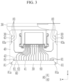
- FIG. 3 is a top plan view schematically illustrating a configuration in which a conductive pad portion and a fixing pad portion are formed at an interconnection location of a flexible printed circuit and a DIP connector of FIG. 2 .
- DIP dual-in-line plug
- a rechargeable battery pack 100 includes a cell assembly 10 including at least one battery cell 11, a frame portion 20 accommodating the cell assembly 10, a flexible printed circuit (FPC) 30 electrically connected to the cell assembly 10 and configured to sense or detect at least one property of the battery cell 11, and a DIP connector 40 electrically connected to the flexible printed circuit 30 and installed on a first side of the frame portion 20.
- FPC flexible printed circuit
- a plurality of battery cells 11 may be composed of ordinary rechargeable batteries that are configured to repeatedly perform charging and discharging operations.
- the frame portion 20 may include a first side frame 21 configured to support a first side surface of a plurality of battery cells 11, a second side frame 22 configured to support a second side surface of the plurality of battery cells 11, a first end frame 23 having ends connected to respective first ends of the first side frame 21 and the second side frame 22, and a second end frame 24 having ends connected to respective second ends of the first side frame 21 and the second side frame 22.
- the first side frame 21 may be installed to support first sides of the plurality of battery cells 11.
- the second side frame 22 may be installed to support second sides of the plurality of battery cells 11.
- the first end frame 23 may be installed to connect between the first ends of the first side frame 21 and the second side frame 22. That is, a first end of the first end frame 23 may be connected to a first end of the first side frame 21 by a fastening member, and a second end thereof may be connected to a first end of the second side frame 22 by a fastening member.
- the second end frame 24 may be installed to connect between the second ends of the first side frame 21 and the second side frame 22. That is, a first end of the second end frame 24 may be connected to a second end of the first side frame 21 by a fastening member, and a second end of the second end frame 24 may be connected to a second end of the second side frame 22 by a fastening member.
- the flexible printed circuit (FPC) 30, which is electrically connected to the cell assembly 10 and is configured to sense or determine at least one property of the battery cell 11, may be installed in an upper portion of the frame portion 20.
- the flexible printed circuit 30 may be installed to sense or determine voltage, temperature, or the like, of the battery cell 11.
- a plurality of circuit lines 42 of the flexible printed circuit 30 may be electrically connected to the DIP connector 40 at a side surface of the frame portion 20.
- the DIP connector 40 is installed on a first side position of the cell assembly 10, and in the present embodiment, may be installed at a location of the second end frame 24, to be electrically connected to the flexible printed circuit 30.
- the present disclosure is not limited to the DIP connector 40 being installed at a location of the second end frame 24, and in one or more embodiments the installation position of the DIP connector 40 may depend on the position of the first end frame 23 or the like.
- the DIP connector 40 and the flexible printed circuit 30 are electrically interconnected to each other by an electrically conductive adhesive 50.
- the DIP connector 40 and the flexible printed circuit 30 are electrically connected to each other by using an electrically conductive adhesive such as a solder without using a separate terminal, and thus disconnection at the connection portion of the circuit due to compression damage may be prevented.
- the electrically conductive adhesive 50 may be applied as a solder to electrically connect the flexible printed circuit 30 and the DIP connector 40. In one or more embodiments, the electrically conductive adhesive 50 may be applied as a conductive glue.
- solder as the electrically conductive adhesive 50 will be described as an example, and the same reference numeral will be used for the electrically conductive adhesive and the solder in the following description.
- a conductive pad portion 60 for bonding the solder 50 may be formed on the DIP connector 40.
- a first groove 41 for connection to the flexible printed circuit 30 and the conductive pad portion 60 may be formed in the DIP connector 40.
- the rear side of the DIP connector 40 is installed in a configuration in which it is in surface contact with a surface of the flexible printed circuit 30, and the first groove 41 may be formed on the first side surface of the DIP connector 40.
- the first groove 41 is formed at an edge of the first side of the DIP connector 40 and may be formed to extend from the first side of the DIP connector 40 toward the inside.
- the conductive pad portion 60 connected to the circuit line 42 formed in the DIP connector 40 may be formed in the first groove 41.
- the flexible printed circuit 30 may be electrically connected to the DIP connector 40 by the conductive pad portion 60 formed at the edge of the first groove 41.
- the conductive pad part 60 is a portion that is formed at the edge of the first groove 41 formed in the DIP connector 40 and to which the solder 50 is bonded, and may electrically connect the flexible printed circuit 30 to a circuit line 31 of the DIP connector 40.
- the conductive pad portion 60 protrudes from the circuit line 42 in a size larger than the width of the circuit line 42, and thus may electrically interconnect the flexible printed circuit 30 and the DIP connector 40 by the solder 50.
- FIG. 4 schematically illustrates a configuration in which the flexible printed circuit and the DIP connector of FIG. 3 are electrically interconnected to each other by electrically conductive adhesive (e.g., solder).
- FIG. 5 schematically illustrates a configuration in which an electrically conductive adhesive is omitted from a conductive pad portion of a first groove of FIG. 3 .
- FIG. 6 schematically illustrates a configuration in which a first pad of a fixing pad portion is formed on side surface of a conductive pad portion of a first groove of FIG. 3 .
- the conductive pad portion 60 may include a first expansion pad 61 protruding from a first side of a width direction of the circuit line 42, and a second expansion pad 63 protruding from a second side of the width direction of the circuit line 42.
- the first side and the second side are directions opposite to each other.
- the first expansion pad 61 may protrude in a first side direction relative to a center of an end of the circuit line 42.
- the first expansion pad 61 may be formed of a material the same as or similar to the material of the circuit line 42 and may protrude in a curved (e.g., round) shape in the first side direction while being connected to the circuit line 42.
- the second expansion pad 63 may protrude from the circuit line 42 in a second side direction opposite to the first side direction in the same or similar shape as the first expansion pad 61 (e.g., the first expansion pad 61 and the second expansion pad 63 may be symmetric).
- the first expansion pad 61 and the second expansion pad 63 which are electrically connected to the end portion of the circuit line 42, each protrude in a curved (e.g., round) shape in opposite directions, and a first curved opening (e.g., round hole) 62 may be formed between the first expansion pad 61 and the second expansion pad 63.
- the first round hole 62 between the first expansion pad 61 and the second expansion pad 63 a sufficient space for filling the solder 50 may be provided or obtained and a surface area of a portion applied with the solder 50 is increased, thereby achieving a more robust electrical connection.
- the application area of the solder 50 may be maximized or at least increased compared to a configuration in which the first expansion pad 61 and the second expansion pad 63 are not formed.
- a conformal coating 70 (refer to FIG. 4 ) may be applied to a surface of the solder 50 connecting between the flexible printed circuit 30 and the DIP connector 40.
- the conformal coating 70 may be applied to cover an entire outer surface (or substantially an entire outer surface) of the plurality of cured solders 50 to connect the flexible printed circuit 30 and the DIP connector 40.
- the conformal coating 70 may be applied to the conductive pad portion 60 around the edge of the first groove 41 of the DIP connector 40 to entirely cover (or substantially entirely cover) the cured solder 50.
- the conformal coating 70 is applied with a sufficient width to cover (or substantially cover) both a part of the DIP connector 40 and a part of the flexible printed circuit 30 around the first groove 41, and may be applied with a sufficient length along a length direction of the first groove 41 to entirely cover (or substantially entirely cover) the cured solder 50 at the conductive pad portion 60.
- the conformal coating 70 may more stably maintain durability of (e.g., protect) the portion to which the solder 50 is applied.
- the rechargeable battery pack 100 may include a fixing pad portion 80 for fixing the flexible printed circuit 30 and the DIP connector 40 to each other.
- the fixing pad part 80 may be formed to provide a fixing force such that the flexible printed circuit 30 and the DIP connector 40 are more stably fixed to each other.
- the fixing pad portion 80 is formed on the interconnected location of the flexible printed circuit 30 and the DIP connector 40 to be applied with the solder 50, and may more stably fix the flexible printed circuit 30 and the DIP connector 40 by the adherence of the solder 50.
- the fixing pad portion 80 may be formed on a part of the first groove 41 of the DIP connector 40 in which the conductive pad portion 60 is located, and a side surface of a width direction of a part of the DIP connector 40, respectively.
- the fixing pad portion 80 may fix the flexible printed circuit 30 and the DIP connector 40 by the adherence of the solder 50, at a portion where the circuit line 42 of the DIP connector 40 is not formed. That is, the solder 50 applied to the fixing pad part 80 provides fixing force by adhesive force rather than electrical connection between the flexible printed circuit 30 and the DIP connector 40.
- a second groove 43 may be further formed on the side surface of the DIP connector 40.
- the DIP connector 40 may include two second grooves 43.
- the second grooves 43 may be formed on opposite sides of the DIP connector 40 in the width direction.
- the fixing pad part 80 may include a first pad 81 formed in the first groove 41 and a second pad 83 formed in the second groove 43.
- the fixing pad part 80 may include a plural quantity (e.g., two or more) of second pads 83 in each of the second grooves 43.
- the first pad 81 is formed in the first groove 41, and may be formed in a plural quantity (e.g., two or more) in the first groove 41 at a portion where the circuit line 42 of the DIP connector 40 is not formed.
- the DIP connector 40 and the flexible printed circuit 30 may be stably connected to each other by the adhesive force of the solder 50.
- a second curved opening (e.g., round hole) 81a may be formed inside the first pad 81 to enlarge an area to which the solder 50 is applied.
- the second round hole 81a may be formed in a substantially semicircular shape, such that the solder 50 may be applied to a sufficient contact area.
- the first pads 81 are formed at locations spaced apart from a plurality of conductive pad portions 60 formed in the first groove 41, and may be formed at both side edge positions of the first groove 41.
- first pads 81 may be formed on opposite sides of the first groove 41 with the plurality of conductive pad portions 60 interposed therebetween.
- solder 50 is applied to conductive pad portions 60, and the first pad 81 may enable the electrical connection of the flexible printed circuit 30 and the DIP connector 40 to be more stably maintained.
- the first pad 81 may be formed to prevent separation of the electrical connection between the flexible printed circuit 30 and the DIP connector 40, thereby increasing durability.
- the first pad 81 may be formed in a single quantity or in a plural quantity at a position spaced apart from the plurality of conductive pad parts 60 in the first groove 41.
- the first pad 81 is not necessarily limited to being formed at both edge positions of the first groove 41, and it is possible to be formed between the plurality of conductive pad parts 60 to provide a more effective fixing force.
- the first groove 41 may be connected with an inclined groove 41a (see FIG. 6 ) connected to an edge of the DIP connector 40.
- the inclined grooves 41a are formed on both sides of the first groove 41 and are formed in a straight line shape, and the first pad 81 may be formed on the inner wall surface thereof. Therefore, since the first pad 81 is formed in a plural quantity at locations close to the portion where the conductive pad unit 60 is formed, the flexible printed circuit 30 and the DIP connector 40 may be more stably interconnected to each other.
- the second pad 83 is formed on the inner wall surfaces of the second grooves 43 formed on opposite sides of the DIP connector 40 in the width direction, respectively, such that the connection of the flexible printed circuit 30 and the DIP connector 40 may be further secured.
- the second pad 83 is formed in the second groove 43, and may be formed in a plural quantity in the second groove 43 at a portion where the circuit line 42 of the DIP connector 40 is not formed.
- solder 50 is applied to the second pad 83, the DIP connector 40 and the flexible printed circuit 30 may be stably connected to each other by the adhesive force of the solder 50.
- a third curved opening (e.g., round hole) 83a may be formed inside the second pad 83 to enlarge an area to which the solder 50 is applied.
- the third round hole 83a may be formed in a substantially semicircular shape, such that the solder 50 may be applied to a sufficient contact area. That is, the third round hole 83a is formed in a shape similar to the second round hole 81a formed in the first pad 81, and they may be formed in a semicircular shape having the same or similar curvature to each other.
- the second round hole 81a and the third round hole 83a are illustratively described as having the same or similar curvature to each other, but are not necessarily limited thereto, and it is possible to appropriately change the curvature in order to increase the fixing force of the flexible printed circuit 30 and the DIP connector 40 (e.g., the second round hole 81a and the third round hole 83a may have different shapes and/or different sizes).
- the second groove 43 is formed on opposite sides of the DIP connector 40 with a length shorter than the length of the first groove 41, and a plurality of second pads 83 may be formed on the inner wall surface thereof.
- three second pads 83 on the inner wall surface of the second groove 43 will be described as an example. However, the present disclosure is not limited to three second pads 83 being formed on the inner wall surface of the second groove 43, and there may be any other suitable number of second pads 83 to change the size or fixing force of the DIP connector 40.
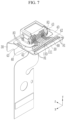
- FIG. 7 is a perspective view schematically illustrating a configuration in which a conductive pad portion and a sub-pad portion are formed at an interconnection location of a flexible printed circuit and a DIP connector according to a second embodiment of the present disclosure.
- FIG. 8 is a top plan view schematically illustrating a configuration in which a conductive pad portion and a sub-pad portion are formed at an interconnection location of a flexible printed circuit and a DIP connector of FIG. 7 .
- the same reference numerals as those in FIG. 1 to FIG. 6 denote the same or similar elements having the same or similar functions. In the following, the same reference numerals are not described in detail again.
- a sub-pad portion 110 may be formed at locations spaced apart from the conductive pad portion 60.
- the sub pad portion 110 is applied with solder 50 therein, and may be formed to electrically connect the DIP connector 40 and the flexible printed circuit 30 to each other.
- the sub-pad portion 110 is formed to protrude from the circuit line 42 of the DIP connector 40 at a position spaced a certain distance from the conductive pad part 60, and a through hole 111 may be formed in the sub-pad portion 110.
- the sub-pad portion 110 protrudes in a curved (e.g., round) shape from the circuit line 42 at a position spaced apart from the conductive pad part 60, and the sub-pad portion 110 may protrude while being electrically connected to the circuit line 42.
- the sub-pad part 110 protrudes from the circuit line 42 in a round shape by way of example, it is not necessarily limited thereto and may be changed into various shapes including a polygonal shape.
- solder 50 is inserted into the through hole 111 of the sub-pad portion 110 to electrically connect the flexible printed circuit board 30 and the DIP connector 40 to each other, thereby providing a more robust electrical connection.
- FIG. 9 is a perspective view schematically illustrating a configuration in which a conductive pad portion and a gas discharging portion are formed at an interconnection location of a flexible printed circuit and a DIP connector according to a third embodiment of the present disclosure.
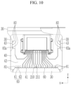
- FIG. 10 is a top plan view schematically illustrating a configuration in which a conductive pad portion and a gas discharging portion are formed at an interconnection location of a flexible printed circuit and a DIP connector of FIG. 9 .
- the same reference numerals as those in FIG. 1 to FIG. 8 denote similar elements having the same or similar functions, and detailed description thereof will be omitted below.
- the DIP connector 40 of a rechargeable battery pack may have a gas discharging portion 210 formed at a location spaced apart from the conductive pad portion 60.
- the gas discharging portion 210 is connected to a part of the plurality of circuit lines 42 at a side surface position of the conductive pad portion 60, and may be applied as a third pad having a gas discharge hole 211 formed therein.
- the same reference numerals are used for the gas discharge unit and the third pad.
- a third pad 210 is formed on the DIP connector 40 at a side surface position of the conductive pad part 60, and it may be formed on a portion of the plurality of circuit lines 42 formed on the DIP connector 40.
- the gas discharge hole 211 may be formed in the third pad 210.
- the gas discharge hole 211 is described as being formed in a single quantity in the third pad 210, but is not necessarily limited thereto and may be formed in a plural quantity (e.g., there may be two or more gas discharge holes 211).
- gas generated in the process of connecting the DIP connector 40 and the flexible printed circuit 30 to each other by applying the solder 50 to the conductive pad portion 60 may be easily discharged through the gas discharge hole 211 to the outside. Accordingly, the fixing force by the solder 50 is further improved, and durability of electrical connection between the DIP connector 40 and the flexible printed circuit 30 may be improved.
- the third pad 210 has a generally rectangular planar shape and may be formed at the side surface of the conductive pad unit 60.
- the third pad 210 is not necessarily limited to a rectangular planar shape, and in one or more embodiments a portion or the entire edge of the third pad 210 may also include a curved (e.g., round) shape.
- the third pad 210 may be formed on some of the plurality of circuit lines 42 formed in the DIP connector 40 (e.g., the third pad 210 may not be applied to each of the circuit lines 42). In one or more embodiments, the third pad 210 may be formed on alternate circuit lines 42 (e.g., the third pad 210 may be on every other circuit line 42), such as an even-numbered circuit line or an odd-numbered circuit line among the plurality of circuit lines 42.
- the gas generated in the process of applying and curing the solder 50 may be easily discharged to the outside through the gas discharge hole 211, the fixing force by the solder 50 is further improved and durability of the electrical connection of the flexible printed circuit 30 and the DIP connector 40 may be improved.
- cell assembly 11 battery cell 20: frame portion 21: first side frame 22: second side frame 23: first end frame 24: second end frame 30: flexible printed circuit 40: DIP connector 41: first groove 41a: inclined groove 42: circuit line 43: second groove 50: electrically conductive adhesive, solder 60: conductive pad portion 61: first expansion pad 62: first round hole 63: second expansion pad 70: conformal coating 80: fixing pad portion 81: first pad 81a: second round hole 83: second pad 83a: third round hole 110: sub-pad portion 111: through hole 210: gas discharging portion, third pad 211: gas discharging hole
Landscapes
- Chemical & Material Sciences (AREA)
- Chemical Kinetics & Catalysis (AREA)
- Electrochemistry (AREA)
- General Chemical & Material Sciences (AREA)
- Engineering & Computer Science (AREA)
- Microelectronics & Electronic Packaging (AREA)
- Manufacturing & Machinery (AREA)
- Coupling Device And Connection With Printed Circuit (AREA)
- Battery Mounting, Suspending (AREA)
Applications Claiming Priority (1)
| Application Number | Priority Date | Filing Date | Title |
|---|---|---|---|
| KR1020230007008A KR20240114636A (ko) | 2023-01-17 | 2023-01-17 | 이차전지 팩 |
Publications (2)
| Publication Number | Publication Date |
|---|---|
| EP4407771A2 true EP4407771A2 (fr) | 2024-07-31 |
| EP4407771A3 EP4407771A3 (fr) | 2024-11-27 |
Family
ID=89223785
Family Applications (1)
| Application Number | Title | Priority Date | Filing Date |
|---|---|---|---|
| EP23217528.1A Pending EP4407771A3 (fr) | 2023-01-17 | 2023-12-18 | Bloc-batterie rechargeable |
Country Status (4)
| Country | Link |
|---|---|
| US (1) | US20240243499A1 (fr) |
| EP (1) | EP4407771A3 (fr) |
| KR (1) | KR20240114636A (fr) |
| CN (1) | CN118367310A (fr) |
Family Cites Families (5)
| Publication number | Priority date | Publication date | Assignee | Title |
|---|---|---|---|---|
| JP3998732B2 (ja) * | 1994-08-31 | 2007-10-31 | エスティーマイクロエレクトロニクス,インコーポレイテッド | 回路部品パッケージ及びその製造方法 |
| TWI540469B (zh) * | 2014-04-01 | 2016-07-01 | 原相科技股份有限公司 | 高靜電防護之電子裝置 |
| KR102033001B1 (ko) * | 2017-02-28 | 2019-10-16 | 주식회사 유라코퍼레이션 | 프레임 조립체, 프레임 조립체의 제조 방법 및 배터리 모듈의 제조 방법 |
| WO2018124751A1 (fr) * | 2016-12-27 | 2018-07-05 | 주식회사 유라코퍼레이션 | Carte de circuit imprimé souple et ensemble cadre la comprenant |
| KR102150679B1 (ko) * | 2018-03-13 | 2020-09-01 | 주식회사 엘지화학 | 배터리 모듈, 이러한 배터리 모듈을 포함하는 배터리 팩 및 이러한 배터리 팩을 포함하는 자동차 |
-
2023
- 2023-01-17 KR KR1020230007008A patent/KR20240114636A/ko active Pending
- 2023-10-05 US US18/481,890 patent/US20240243499A1/en active Pending
- 2023-12-13 CN CN202311725738.XA patent/CN118367310A/zh active Pending
- 2023-12-18 EP EP23217528.1A patent/EP4407771A3/fr active Pending
Also Published As
| Publication number | Publication date |
|---|---|
| KR20240114636A (ko) | 2024-07-24 |
| EP4407771A3 (fr) | 2024-11-27 |
| CN118367310A (zh) | 2024-07-19 |
| US20240243499A1 (en) | 2024-07-18 |
Similar Documents
| Publication | Publication Date | Title |
|---|---|---|
| US9716258B2 (en) | Battery pack | |
| CN110521017B (zh) | 电池包 | |
| CN110114932A (zh) | 电池模块以及包括电池模块的电池组和车辆 | |
| US10439180B2 (en) | Battery module | |
| KR102577098B1 (ko) | 배터리 모듈 | |
| CN117293375A (zh) | 二次电池 | |
| US9997809B2 (en) | Battery module | |
| KR101494151B1 (ko) | 기계적 체결 방식에 의해 전기적으로 접속되는 커넥터를 포함하는 전지모듈 | |
| KR102785764B1 (ko) | 이차 전지 | |
| US8632899B2 (en) | Battery pack | |
| EP4044348A1 (fr) | Bloc-batterie | |
| EP4407771A2 (fr) | Bloc-batterie rechargeable | |
| EP4518005A1 (fr) | Ensemble structure de borne comprenant une barre omnibus d'un seul tenant | |
| US20230378620A1 (en) | Pouch-type battery cell, and battery cell assembly and battery pack having the same | |
| WO2017188582A2 (fr) | Batterie rechargeable | |
| US20240234838A1 (en) | Rechargeable battery pack | |
| EP3846282A1 (fr) | Bloc-batterie | |
| JPH1145690A (ja) | 電池モジュ−ル | |
| EP4407744B1 (fr) | Bloc-batterie rechargeable | |
| EP4583240A1 (fr) | Batterie de type poche | |
| US20240170817A1 (en) | Rechargeable battery pack | |
| KR102778063B1 (ko) | 배터리 팩 | |
| EP4730925A2 (fr) | Ensemble carte de circuit imprimé et batterie rechargeable le comprenant | |
| KR20260055115A (ko) | 기판 조립체 및 이를 포함하는 이차 전지 | |
| KR20250021005A (ko) | 배터리 어셈블리 |
Legal Events
| Date | Code | Title | Description |
|---|---|---|---|
| PUAI | Public reference made under article 153(3) epc to a published international application that has entered the european phase |
Free format text: ORIGINAL CODE: 0009012 |
|
| STAA | Information on the status of an ep patent application or granted ep patent |
Free format text: STATUS: REQUEST FOR EXAMINATION WAS MADE |
|
| 17P | Request for examination filed |
Effective date: 20231218 |
|
| AK | Designated contracting states |
Kind code of ref document: A2 Designated state(s): AL AT BE BG CH CY CZ DE DK EE ES FI FR GB GR HR HU IE IS IT LI LT LU LV MC ME MK MT NL NO PL PT RO RS SE SI SK SM TR |
|
| PUAL | Search report despatched |
Free format text: ORIGINAL CODE: 0009013 |
|
| AK | Designated contracting states |
Kind code of ref document: A3 Designated state(s): AL AT BE BG CH CY CZ DE DK EE ES FI FR GB GR HR HU IE IS IT LI LT LU LV MC ME MK MT NL NO PL PT RO RS SE SI SK SM TR |
|
| RIC1 | Information provided on ipc code assigned before grant |
Ipc: H05K 1/18 20060101ALI20241024BHEP Ipc: H01M 50/519 20210101ALI20241024BHEP Ipc: H01L 23/58 20060101ALI20241024BHEP Ipc: H01M 50/284 20210101AFI20241024BHEP Ipc: H05K 7/10 20060101ALI20241024BHEP |