EP4407651A1 - Power control method and apparatus for lower radio frequency power source, and semiconductor processing device - Google Patents
Power control method and apparatus for lower radio frequency power source, and semiconductor processing device Download PDFInfo
- Publication number
- EP4407651A1 EP4407651A1 EP22871990.2A EP22871990A EP4407651A1 EP 4407651 A1 EP4407651 A1 EP 4407651A1 EP 22871990 A EP22871990 A EP 22871990A EP 4407651 A1 EP4407651 A1 EP 4407651A1
- Authority
- EP
- European Patent Office
- Prior art keywords
- lower electrode
- power
- circuit
- processing chamber
- processing
- Prior art date
- Legal status (The legal status is an assumption and is not a legal conclusion. Google has not performed a legal analysis and makes no representation as to the accuracy of the status listed.)
- Pending
Links
Images



Classifications
-
- H—ELECTRICITY
- H01—ELECTRIC ELEMENTS
- H01J—ELECTRIC DISCHARGE TUBES OR DISCHARGE LAMPS
- H01J37/00—Discharge tubes with provision for introducing objects or material to be exposed to the discharge, e.g. for the purpose of examination or processing thereof
- H01J37/32—Gas-filled discharge tubes
- H01J37/32009—Arrangements for generation of plasma specially adapted for examination or treatment of objects, e.g. plasma sources
- H01J37/32082—Radio frequency generated discharge
- H01J37/32174—Circuits specially adapted for controlling the RF discharge
-
- H—ELECTRICITY
- H01—ELECTRIC ELEMENTS
- H01J—ELECTRIC DISCHARGE TUBES OR DISCHARGE LAMPS
- H01J37/00—Discharge tubes with provision for introducing objects or material to be exposed to the discharge, e.g. for the purpose of examination or processing thereof
- H01J37/02—Details
- H01J37/248—Components associated with high voltage supply
-
- H—ELECTRICITY
- H01—ELECTRIC ELEMENTS
- H01J—ELECTRIC DISCHARGE TUBES OR DISCHARGE LAMPS
- H01J37/00—Discharge tubes with provision for introducing objects or material to be exposed to the discharge, e.g. for the purpose of examination or processing thereof
- H01J37/32—Gas-filled discharge tubes
- H01J37/32009—Arrangements for generation of plasma specially adapted for examination or treatment of objects, e.g. plasma sources
- H01J37/32082—Radio frequency generated discharge
- H01J37/32174—Circuits specially adapted for controlling the RF discharge
- H01J37/32183—Matching circuits
-
- H—ELECTRICITY
- H01—ELECTRIC ELEMENTS
- H01J—ELECTRIC DISCHARGE TUBES OR DISCHARGE LAMPS
- H01J37/00—Discharge tubes with provision for introducing objects or material to be exposed to the discharge, e.g. for the purpose of examination or processing thereof
- H01J37/32—Gas-filled discharge tubes
- H01J37/32431—Constructional details of the reactor
- H01J37/32532—Electrodes
- H01J37/32577—Electrical connecting means
-
- H—ELECTRICITY
- H01—ELECTRIC ELEMENTS
- H01J—ELECTRIC DISCHARGE TUBES OR DISCHARGE LAMPS
- H01J37/00—Discharge tubes with provision for introducing objects or material to be exposed to the discharge, e.g. for the purpose of examination or processing thereof
- H01J37/32—Gas-filled discharge tubes
- H01J37/32431—Constructional details of the reactor
- H01J37/32697—Electrostatic control
- H01J37/32706—Polarising the substrate
-
- H—ELECTRICITY
- H01—ELECTRIC ELEMENTS
- H01J—ELECTRIC DISCHARGE TUBES OR DISCHARGE LAMPS
- H01J37/00—Discharge tubes with provision for introducing objects or material to be exposed to the discharge, e.g. for the purpose of examination or processing thereof
- H01J37/32—Gas-filled discharge tubes
- H01J37/32917—Plasma diagnostics
-
- H—ELECTRICITY
- H01—ELECTRIC ELEMENTS
- H01J—ELECTRIC DISCHARGE TUBES OR DISCHARGE LAMPS
- H01J37/00—Discharge tubes with provision for introducing objects or material to be exposed to the discharge, e.g. for the purpose of examination or processing thereof
- H01J37/32—Gas-filled discharge tubes
- H01J37/32917—Plasma diagnostics
- H01J37/32935—Monitoring and controlling tubes by information coming from the object and/or discharge
-
- H—ELECTRICITY
- H03—ELECTRONIC CIRCUITRY
- H03H—IMPEDANCE NETWORKS, e.g. RESONANT CIRCUITS; RESONATORS
- H03H7/00—Multiple-port networks comprising only passive electrical elements as network components
- H03H7/38—Impedance-matching networks
-
- H—ELECTRICITY
- H01—ELECTRIC ELEMENTS
- H01J—ELECTRIC DISCHARGE TUBES OR DISCHARGE LAMPS
- H01J2237/00—Discharge tubes exposing object to beam, e.g. for analysis treatment, etching, imaging
- H01J2237/32—Processing objects by plasma generation
- H01J2237/33—Processing objects by plasma generation characterised by the type of processing
- H01J2237/334—Etching
-
- H—ELECTRICITY
- H01—ELECTRIC ELEMENTS
- H01J—ELECTRIC DISCHARGE TUBES OR DISCHARGE LAMPS
- H01J37/00—Discharge tubes with provision for introducing objects or material to be exposed to the discharge, e.g. for the purpose of examination or processing thereof
- H01J37/32—Gas-filled discharge tubes
- H01J37/32009—Arrangements for generation of plasma specially adapted for examination or treatment of objects, e.g. plasma sources
- H01J37/32082—Radio frequency generated discharge
- H01J37/321—Radio frequency generated discharge the radio frequency energy being inductively coupled to the plasma
Definitions
- the present disclosure generally relates to the semiconductor manufacturing field and, more particularly, to a power control method and a power control device for a lower radio frequency power supply in semiconductor processing equipment, and the semiconductor processing equipment.
- the lower RF power supply loads the RF energy to the lower electrode (e.g., electrostatic chuck) through a matcher.
- the lower electrode e.g., electrostatic chuck
- an RF bias voltage is generated on the wafer surface to accelerate the etching of the ions on the wafer.
- the bias voltage generated at the wafer can change, and the final etching processing result can change too.
- the consistency of the overall efficiency of the lower electrode RF circuit can be closely related to the processing result.
- the power loss generated in the process from outputting the RF power by the lower electrode power supply until the RF power is adopted by the plasma includes matcher loss, loss of the lower electrode for the ground capacity, and circuit contact loss.
- matcher loss loss of the lower electrode for the ground capacity
- circuit contact loss the equivalent resistance and capacity of various parts of the lower electrode RF circuit can be different. That is, the power loss can be different.
- the power adopted by plasma can be different too.
- the generated RF bias voltages can be different, which affects the consistency of the processing result.
- the present disclosure is intended to solve one of the technical problems in the existing technology and provides a power control method and a power control device of a lower RF power supply of semiconductor processing equipment and the semiconductor processing equipment, which improves processing result consistency of different processing chambers.
- the power control method of the lower RF power supply of the semiconductor processing equipment includes:
- acquisition methods of the loss equivalent resistance and the grounded equivalent resistance of the lower electrode RF circuit for each processing chamber include:
- the semiconductor processing includes a plurality of processing steps.
- the power control method further includes:
- obtaining the power compensation value of the present processing chamber relative to the reference chamber includes: calculating a product of the power compensation coefficient and the power setting value as the power compensation value.
- the present disclosure further provides a power control device of a lower RF power supply of semiconductor processing equipment including a calculation unit and a control unit.
- control unit is further configured to turn on the lower RF power supply of the processing chamber to apply a determined power value to the lower electrode through the matcher to ensure that plasma in the processing chamber does not ignite;
- the semiconductor processing includes a plurality of processing steps
- the calculation unit is configured to calculate a product of the power compensation coefficient and the power setting value as the power compensation value.
- the present disclosure further provides semiconductor processing equipment, including a processing chamber, an matcher, and a lower RF power supply, wherein a lower electrode is arranged in the processing chamber, the lower electrode is electrically connected to the lower RF power supply through the matcher, and the semiconductor processing equipment further includes the power control device of the present disclosure.
- the present disclosure has the following beneficial effects.
- the power compensation coefficient can be obtained.
- the power compensation value can be calculated.
- the lower RF power supply can be controlled to output the power compensation value.
- the semiconductor processing equipment of the present disclosure by adopting the power control device of the present disclosure, can improve the consistency of the bias voltage value generated on the wafer among different chambers under the same processing recipe to improve the consistency of processing results among different process chambers.
- FIG. 1 illustrates a schematic structural diagram of an inductively coupled plasma equipment.
- the equipment includes a processing chamber 11.
- a dielectric window 6 is arranged at the top of the processing chamber.
- An inductive coupling coil 5 is arranged above the dielectric window 6.
- the inductive coupling coil 5 is electrically connected to an upper RF power supply 1 via an upper matcher 2.
- the upper RF power supply 1 can apply RF power onto the inductive coupling coil 5 via the upper matcher 2 to excite a process gas in the processing chamber 11 to form a plasma 9.
- a lower electrode 8 e.g., an electrostatic chuck
- the lower electrode 8 is electrically connected to a lower RF power supply 4 via a lower matcher 3.
- the lower RF power supply 4 is configured to apply RF power onto the lower electrode 8 to generate an RF bias voltage on the wafer surface to accelerate ions to etch the wafer 7.
- the RF bias voltage can be used to accelerate the ions to perform an etching process.
- the applied RF power is different, the magnitude of the bias voltage on the wafer 7 can change, and the final etching process result can change.
- the overall efficiency consistency of the lower electrode circuit can be closely related to the process results.
- FIG. 2A illustrates a schematic diagram showing radio frequency (RF) power loss in a lower electrode RF circuit in FIG. 1 .
- the power loss during the process from the RF power output from the lower RF power supply 4 to the power utilized by the plasma 9 mainly includes losses in the matcher, losses in the lower electrode to ground capacitance, losses in circuit contact, etc.
- the output power of the lower RF power supply 4 is P in
- the total power loss of the lower electrode RF circuit can be P 0
- the remaining power utilized by the plasma 9 can be P p
- FIG. 2B illustrates an equivalent circuit diagram of the lower electrode RF circuit in FIG. 1 .
- capacitor C1 and capacitor C2 are variable capacitors in lower matcher 3.
- a loss resistance of the lower matcher 3 and a contact resistance of the lower electrode RF circuit as a whole can be considered as a loss equivalent resistance R m of the lower electrode RF circuit.
- the loss equivalent resistance R m is connected in series in the main path of the lower electrode RF circuit.
- an equivalent circuit connected to an output end of the main path can include two parallel branches.
- One of the branches can be a lower electrode-to-ground branch.
- the lower electrode-to-ground branch can include a lower electrode-to-ground capacitance C and an equivalent resistance R g when the lower electrode is grounded.
- the other branch can be a plasma sheath branch.
- the plasma sheath branch can include an impedance real part R p and an equivalent inductance L p of an impedance imaginary part of the plasma 9, and an impedance real part R s and an equivalent capacitance C s of an impedance imaginary part of the plasma sheath.
- the current in the lower electrode-to-ground branch can be I c
- the current in the plasma sheath branch can be I s
- the current at the output end of the lower matcher 3 in the main path of the lower electrode RF circuit can be I.
- the current I can be equal to the sum of the currents I c and I s .
- the matcher in the lower electrode RF circuit, the lower electrode, the installation contact resistance, etc. are different, the equivalent resistance and capacitance of the parts of the lower electrode RF circuit can be different among different chambers. That is, the total power loss P 0 in the lower electrode RF circuit can be different.
- the remaining power P p utilized by the plasma 9 the power transmission efficiency ⁇
- the RF bias voltage generated on the wafer surface can be different, which affects the consistency of the processing results.
- FIG. 3 illustrates a schematic block diagram of a power control method of a lower RF power supply in semiconductor processing equipment according to embodiments of the present disclosure.
- the method includes the following steps.
- a power compensation coefficient of the present processing chamber is obtained relative to the reference chamber.
- the reference chamber above can be one chamber specified from a plurality of chambers with the same structure.
- the first RF circuit parameter set of the reference chamber can refer to a combination of feature parameters of the lower electrode of the reference chamber.
- This first RF circuit parameter set can include but is not limited to the current at the output end of the lower matcher 3 in the main path of the lower electrode RF circuit, the current in the plasma sheath branch of the lower electrode RF circuit, the loss equivalent resistance and the ground equivalent resistance of the lower electrode RF circuit, and the lower electrode-to-ground capacitance.
- the present processing chamber above can be other processing chambers with the same structure except the reference chamber.
- compensation can be performed on the output power of the lower RF power supply 4 according to the inherent parameter of the processing chambers (i.e., the second RF circuit parameter set) and in connection with the inherent parameter and the plasma sheath parameter of the reference chamber (i.e., the first RF circuit parameter set) to achieve that the RF bias voltage generated on the wafer surface when the processing is performed in the other processing chambers with the same structure is consistent with the reference chamber.
- the second RF circuit parameter set of the present processing chamber can include but is not limited to the loss equivalent resistance and the grounded equivalent resistance of the lower RF circuit and the lower electrode-to-ground capacitance.
- the inherent parameters such as the loss equivalent resistance R m , the grounded equivalent resistance R g , and the lower electrode-to-ground capacitance C can remain unchanged when performing the processing.
- the plasma sheath parameter of the lower electrode RF circuit e.g., the RF bias voltage and the current in the plasma sheath branch
- the current I c in the lower electrode-to-ground branch is made of most of the current I (usually greater than 10 amperes).
- the current I s in the plasma sheath branch can be small (smaller than 1 ampere).
- the current I s in the plasma sheath branch can be regarded as a constant current.
- the remaining power P p utilized by the plasma 9 (also referred to as absorption power) is a product of the RF bias voltage and the current I s in the plasma sheath branch, the remaining power P p can also change with the processing. Based on this, the lower electrode loss feature of different chambers can be reflected by the inherent parameters and the plasma sheath parameters. The difference in the remaining power P p between the other processing chambers and the reference chamber can be compensated according to the lower electrode loss feature to allow different chambers to have the same remaining power P p . Thus, the RF bias voltages of different chambers can be ensured to be consistent, and the processing results can be consistent.
- a current detection unit 24 is further arranged in the circuit between the output end of the lower matcher 3 and the lower electrode 8 and is configured to detect the current I at the output end of the lower matcher 3 in the main path of the lower electrode RF circuit.
- voltage detection unit 23 is connected to the lower electrode 8 and is configured to detect the RF bias voltage on the wafer surface.
- a capacitance detection unit (not shown in the figure) can be connected to the lower electrode-to-ground branch and be configured to detect the lower electrode-to-ground capacitance C.
- the following acquisition method can be used to obtain the loss equivalent resistance R m and the grounded equivalent resistance R g .
- the lower RF power supply 4 of the processing chamber (the upper RF power supply 1 is turned off) is turned on to apply a power setting value P low on the lower electrode 8 via the lower matcher 3.
- the power setting value P low can be lower than the power value normally used in the processing.
- the determined power P low can be almost fully consumed by the lower electrode-to-ground branch when the lower matcher 3 performs matching. Since the upper RF power supply 1 is turned off, and the power setting value P low is low, the power may not be sufficient to cause the plasma in the processing chamber to ignite. Thus, no plasma load can be generated.
- the current at the output end of the matcher i.e., the lower matcher 3 in the main path of the lower electrode RF circuit, the present bias voltage value of the lower electrode 8, and the lower electrode-to-ground capacitance are detected.
- the current detection unit 24 can be configured to detect the current I 0 at the output end of the matcher in the main path of the lower electrode RF circuit.
- the voltage detection unit 23 can be configured to detect the present bias voltage value V 0 of the lower electrode 8
- the capacitance detection unit can be configured to detect the lower electrode-to-ground capacitance C.
- V 0 I 0 R g 2 + 1 ⁇ C 2
- R g V 0 I 0 2 ⁇ 1 ⁇ C 2
- R m P low I 0 2 ⁇ R g
- R g denotes the grounded equivalent resistance of the lower electrode RF circuit
- R m denotes the loss equivalent resistance of the lower electrode RF circuit
- V 0 denotes the present bias voltage value
- I 0 denotes the present current
- ⁇ denotes an angular frequency
- C denotes the lower electrode-to-ground capacitance
- P low denotes the power setting value.
- the loss equivalent resistance R m and the grounded equivalent resistance R g of the lower electrode RF circuit can also be obtained in any other methods, which are not limited in the present disclosure.
- V 1 I c 1 R g 2 + 1 ⁇ C 2
- I c1 the current in the lower electrode-to-ground branch corresponding to semiconductor processing 1.
- V 2 I c 2 R g 2 + 1 ⁇ C 2
- I c2 the current in the lower electrode-to-ground branch corresponding to semiconductor processing 2.
- the equation for the current I s in the plasma sheath branch can be applied regardless of whether semiconductor processing 1, semiconductor processing 2, or any other different processing.
- step 201 to step 203 can be used to obtain the loss equivalent resistance R mA and grounded equivalent resistance R gA for processing chamber A, the loss equivalent resistance R mB and ground equivalent resistance R gB for processing chamber B, the loss equivalent resistance R mC and grounded equivalent resistance R gC for processing chamber C.
- the capacitance detection unit of processing chamber A can be configured to obtain the lower electrode-to-ground capacitance C A .
- the capacitance detection unit of processing chamber B can be configured to obtain the lower electrode-to-ground capacitance C B .
- the capacitance detection unit of processing chamber C can be configured to obtain the lower electrode-to-ground capacitance Cc.
- the bias voltage values corresponding to different chambers can be different. That is, for example, semiconductor processing 1 is performed, V A1 ⁇ V B1 ⁇ V C1 . Based on this, when the power setting value of the lower electrode power supply 4 of the three processing chambers (A, B, and C) is P in , remaining power P pA , remaining power P pB , and remaining power P pC utilized by the plasma 9 corresponding to the three processing chambers (A, B, and C) can have the following equations.
- I s1 can be the current in the plasma sheath branch corresponding to semiconductor processing 1.
- processing chamber A is selected as the reference chamber, the equation (7) can be used to calculate the current I s1 for processing chamber A.
- the currents in the plasma sheath branches corresponding to semiconductor processing 1 for the other two processing chambers (B and C) can be set to be equal to I s1 .
- ⁇ B 1 V A 1 I s 1 V B 1 I s 1
- an impedance corresponding to the ground capacitance C B of processing chamber B is Y
- I cB 1 ⁇ I s 1 2 R mB + Y + I s 1 2 2 R mB + Y 2 ⁇ 4 R mB + R gB I s 1 2 R mB ⁇ R mA ⁇ I cA 1 2 R mA + R gA ⁇ 2 I s 1 I CA 1 R mA ⁇ I s 1 I CA 1 X 2 R mB + R gB
- ⁇ B 1 is the power compensation coefficient for processing chamber B corresponding to semiconductor processing 1 relative to processing chamber A.
- the first RF circuit parameter set of processing chamber A can include I A , I S , R mA , R gA , and X.
- I A1 is the current at the output end of the matcher in the main path of the lower electrode RF circuit corresponding to semiconductor processing 1.
- I s1 is the current in the plasma sheath circuit branch of the lower electrode RF circuit corresponding to semiconductor processing 1.
- R mA is the loss equivalent resistance of the lower electrode RF circuit of processing chamber A.
- R gA is the grounded equivalent resistance of the lower electrode RF circuit of processing chamber A.
- C A is the lower electrode-to-ground capacitance of processing chamber A.
- the second RF circuit parameter set of processing chamber B can include R mB , R gB , and Y.
- R mB is the loss equivalent resistance of the lower electrode RF circuit of processing chamber B.
- R gB is the grounded equivalent resistance of the lower electrode RF circuit of processing chamber B.
- C B is the lower electrode-to-ground capacitance of processing chamber B.
- ⁇ C 1 is the power compensation coefficient for processing chamber C corresponding to semiconductor processing 1 relative to processing chamber A.
- the second RF circuit parameter set of processing chamber C can include R mC , R gC , and Z.
- R mC is the loss equivalent resistance of the lower electrode RF circuit of processing chamber C.
- R gC is the grounded equivalent resistance of the lower electrode RF circuit of processing chamber C.
- Cc is the lower electrode-to-ground capacitance of processing chamber C.
- semiconductor processing 1 and semiconductor processing 2 above can include two different processing recipes or two different processing steps within the same semiconductor processing.
- the semiconductor processing can include a plurality of processing steps. For different processing steps, the current I s1 in the plasma sheath branch of the lower RF circuit can be different.
- the power control method of embodiments of the present disclosure further includes the following steps.
- pre-obtained I A (the current at the output end of the lower matcher 3 in the main path of the lower RF circuit) and I S (the current in the plasma sheath branch) corresponding to the processing steps are written in a parameter table.
- the processing steps include N steps, and N is an integer greater than 1.
- the I A and I S corresponding to the processing steps can be calculated using the equation (7) above.
- Table 1 shows the parameter table of I A and I S of processing chamber A (i.e., the reference chamber) corresponding to the N processing steps. Step I s I A 1 I s1 I A1 2 I s2 I A2 ... ... ... N IsN I AN
- the pre-obtained R mA , R gA , and C A corresponding to processing chamber A and R mB , R gB , and C B corresponding to processing chamber B are called.
- Step 101 can include:
- each processing step corresponds to an I s , an I A , and a power compensation coefficient.
- the method for obtaining the power compensation coefficient ⁇ Bi corresponding to the i-th processing step is illustrated here only with processing chamber B as an example.
- the other chambers with the same structure except the reference chamber can be suitable for the method for obtaining the power compensation coefficient ⁇ i corresponding to the i-th processing step.
- the power compensation value of the present processing chamber relative to the reference chamber is calculated according to the power compensation coefficient and the power setting value of the lower RF power supply of the present processing chamber.
- step 102 can specifically include: calculating the product of the power compensation coefficient and the power setting value as the power compensation value.
- the lower RF power supply 4 is controlled to output the power compensation value.
- step 103 the power output by the lower RF power supply 4 can be the compensated power value.
- I A and I S corresponding to the next processing step can be called from the parameter table, and the power compensation coefficient corresponding to the next processing step can be calculated again.
- Step 102 and step 103 are used to calculate the power compensation value and perform power compensation on the power setting value (i.e., P in ) output by the lower RF power supply 4.
- the remaining power P P utilized by the plasma 9 of the other chambers with the same structure except the reference chamber can be consistent with the remaining power P P of the reference chamber to ensure that the RF bias voltages of different chambers are consistent to achieve consistent processing results.
- embodiments of the present disclosure also provide a power control device 20 of the lower RF power supply in the semiconductor processing equipment, which includes a calculation unit 21 and a control unit 22.
- the calculation unit 21 can be configured to, when the semiconductor processing begins in the processing chamber, obtain the power compensation coefficient of the present processing chamber relative to the reference chamber by using the predetermined power compensation equation and according to the pre-obtained first RF circuit parameter set of the reference chamber and the second RF circuit parameter set of the present processing chamber that performs the semiconductor processing, and calculate the power compensation value of the present processing chamber relative to the reference chamber according to the power compensation coefficient and the power setting value of the lower RF power supply of the present processing chamber.
- the control unit 22 can be configured to control the lower RF power supply to output the power compensation value.
- the reference chamber can be a determined chamber from the plurality of processing chambers with the same structure.
- the first RF circuit parameter set of the reference chamber can be a combination of the feature parameters of the lower electrode of the reference chamber.
- the first RF circuit parameter set can include but is not limited to the current at the output end of the lower matcher in the main path of the lower electrode RF circuit, the current of the plasma sheath branch of the lower electrode RF circuit, the loss equivalent resistance and the grounded equivalent resistance of the lower electrode RF circuit, and the lower electrode-to-ground capacitance.
- the present processing chamber can be processing chambers with the same structure except the reference chamber.
- the second RF circuit parameter set of the present processing chamber can include but is not limited to the loss equivalent resistance and the grounded equivalent resistance of the lower RF circuit and the lower electrode-to-ground capacitance.
- capacitor C1 and capacitor C2 are both variable capacitors in the lower matcher 3.
- the loss resistance of the lower matcher 3 and the contact resistance of the lower electrode RF circuit as a whole can be considered as the loss equivalent resistance R m of the lower electrode RF circuit.
- the loss equivalent resistance R m can be connected in series in the main path of the lower electrode RF circuit.
- the equivalent circuit part connected to the output end of the main path can include two parallel branches. One of the branches can be a lower electrode-to-ground branch.
- the lower electrode-to-ground branch can include a lower electrode-to-ground capacitance C and an equivalent resistance R g when the lower electrode is grounded.
- the other branch can be a plasma sheath branch.
- the plasma sheath branch can include an equivalent inductance L p of an impedance real part R p and an impedance imaginary part of the plasma 9, and an equivalent capacitance C s of an impedance real part R s and an impedance imaginary part of the plasma sheathr.
- the current in the lower electrode-to-ground branch can be I c
- the current in the plasma sheath branch can be I s
- the current at the output end of the lower matcher 3 in the main path of the lower electrode RF circuit can be I.
- the inherent parameters such as the loss equivalent resistance R m , the grounded equivalent resistance R g , and the lower electrode-to-ground capacitance C can remain unchanged when performing the processing.
- the plasma sheath parameter of the lower electrode RF circuit e.g., the RF bias voltage and the current in the plasma sheath branch
- the current I c in the lower electrode-to-ground branch is made of most of the current I (usually greater than 10 amperes).
- the current I s in the plasma sheath branch can be small (smaller than 1 ampere).
- the current I s in the plasma sheath branch can be regarded as a constant current.
- the remaining power P p utilized by the plasma 9 (also referred to as absorption power) is a product of the RF bias voltage and the current I s in the plasma sheath branch, the remaining power P p can also change with the processing. Based on this, the lower electrode loss feature of different chambers can be reflected by the inherent parameters and the plasma sheath parameters. The difference in the remaining power P p between the other processing chambers and the reference chamber can be compensated according to the lower electrode loss feature to allow different chambers to have the same remaining power P p . Thus, the RF bias voltages of different chambers can be ensured to be consistent, and the processing results can be consistent.
- the first RF circuit parameter set can include I A , I S , R mA , R gA , and X, where I A is the current at the output end of the matcher in the main path of the lower electrode RF circuit.
- I S is the current in the plasma sheath branch of the lower electrode RF circuit of the reference chamber.
- R mA is the loss equivalent resistance of the lower electrode RF circuit of the reference chamber;
- R gA is the grounded equivalent resistance of the lower electrode RF circuit of the reference chamber.
- the second RF circuit parameter set can include R mB , R gB , and Y.
- R mB is the loss equivalent resistance of the lower electrode RF circuit of the present processing chamber.
- R gB is the grounded equivalent resistance of the lower electrode RF circuit of the present processing chamber.
- control unit 22 is also configured to activate the lower RF power supply 4 of the processing chamber and apply the determined power value to the lower electrode 8 through the matcher 3 to ensure that the plasma in the processing chamber does not ignite.
- the lower RF power supply 4 of the processing chamber is activated (the upper RF power supply 1 is turned off).
- the determined power value P low is applied to the lower electrode 8 through matcher 3.
- the determined power value P low can be low compared to the power value adopted by normal processing.
- the determined power value P low when the determined power value P low is applied to the lower electrode, when the lower matcher 3 is paired, the determined power value P low can be consumed by the lower electrode-to-ground branch. Since the RF power supply 1 is turned off, and the determined power value P low is low, the power may not be sufficient to cause the plasma in the processing chamber to ignite. Thus, the plasma load cannot be generated.
- the power control device 20 further includes a current detection unit 24, a voltage detection unit 23, and a capacitance detection unit 25.
- the current detection unit 24 is arranged in the circuit between the output end of the matcher 3 and the lower electrode 8 and configured to detect the present current (i.e., I 0 ) at the output end side of the lower matcher 3 in the main path of the lower electrode RF circuit.
- the voltage detection unit for example, can be electrically connected to the RF electrode of the lower electrode 8 and configured to detect the present bias voltage value of the lower electrode 8 (i.e., V 0 ).
- the capacitance detection unit can be configured to detect the lower electrode-to-ground capacitance (i.e., C) of the lower electrode 8.
- the calculation unit 21 can be further configured to calculate the loss equivalent resistance R m and the grounded equivalent resistance R g of the lower electrode RF circuit using the following equation and the present current I 0 , the present bias voltage value V 0 , and the lower electrode-to-ground capacitance C.
- the equations are as follows.
- R g V 0 I 0 2 ⁇ 1 ⁇ C 2
- R m P low I 0 2 ⁇ R g
- R g the grounded equivalent resistance of the lower electrode RF circuit
- R m the loss equivalent resistance of the lower electrode RF circuit
- V 0 the present bias voltage value
- I 0 the present current
- ⁇ the angular frequency
- C the lower electrode-to-ground capacitance
- P low the determined power value.
- the semiconductor processing can include a plurality of processing steps.
- the power control device 20 can further include a writing unit.
- the writing unit can be configured to write the pre-obtained I A (the current at the output end side of the lower matcher 3 in the main path of the lower electrode RF circuit) and I S (the current in the plasma sheath branch) into the parameter table.
- IA and Is corresponding to the processing steps (Step) can be calculated through the equation (7) of the above embodiments.
- the calculation unit 21 can be further configured to call R mA , R gA , C A , R mB , R gB , and C B .
- I Ai and I Si corresponding to the i-th processing step can be called from the above parameter table.
- the power compensation coefficient ⁇ Bi of processing chamber B corresponding to the i-th processing step.
- the calculation unit 21 can be configured to calculate the product of the power compensation coefficient and the power setting value as the power compensation value.
- the power compensation coefficient can be obtained.
- the power compensation value can be calculated.
- the lower RF power supply can be controlled to output the power compensation value.
- embodiments of the present disclosure further provide semiconductor processing equipment.
- the equipment includes processing chamber 11.
- a dielectric window 6 is arranged at the top of processing chamber 11.
- An inductive coupling coil 5 is arranged above the dielectric window 6.
- the inductive coupling coil 5 can be electrically connected to the upper RF power supply 1 through the upper matcher 2.
- the upper RF power supply 1 can apply the RF power to the inductive coupling coil 5 through the upper matcher 2 to excite the process gas in the processing chamber 11 to generate the plasma 9.
- the lower electrode 8 e.g., the electrostatic chuck
- the lower electrode 8 can be electrically connected to the lower RF power supply 4 through the lower matcher 3.
- the lower RF power supply 4 can be configured to apply the RF power to the lower electrode 8 to generate the RF bias voltage on the wafer surface to accelerate the ions to etch the wafer.
- the semiconductor processing equipment of embodiments of the present disclosure can adopt the power control device of embodiments of the present disclosure.
- the consistency in the bias voltage values generated on the wafers of different chambers under the same processing recipe can be improved.
- the processing result consistency of the different processing chambers can be improved.
Landscapes
- Chemical & Material Sciences (AREA)
- Analytical Chemistry (AREA)
- Physics & Mathematics (AREA)
- Engineering & Computer Science (AREA)
- Plasma & Fusion (AREA)
- Drying Of Semiconductors (AREA)
- Plasma Technology (AREA)
- Chemical Vapour Deposition (AREA)
Abstract
Description
- The present disclosure generally relates to the semiconductor manufacturing field and, more particularly, to a power control method and a power control device for a lower radio frequency power supply in semiconductor processing equipment, and the semiconductor processing equipment.
- As the feature size of integrated circuits continues to decrease, the requirements for processing technology become increasingly strict. One important requirement is product consistency. During the processing process, strict requirements are placed on the consistency of the process results for all chambers in the semiconductor processing equipment of the same model to avoid process risks caused by consistency issues of the chambers. Therefore, strict process control is needed among different chambers to implement consistency in process results.
- Taking inductively coupled plasma equipment as an example, the lower RF power supply loads the RF energy to the lower electrode (e.g., electrostatic chuck) through a matcher. Thus, an RF bias voltage is generated on the wafer surface to accelerate the etching of the ions on the wafer. When the RF power output by the lower RF power supply to the RF power changes, the bias voltage generated at the wafer can change, and the final etching processing result can change too. Thus, the consistency of the overall efficiency of the lower electrode RF circuit can be closely related to the processing result.
- The power loss generated in the process from outputting the RF power by the lower electrode power supply until the RF power is adopted by the plasma includes matcher loss, loss of the lower electrode for the ground capacity, and circuit contact loss. Among different chambers, since the matchers, lower electrode, and mounting contact resistance can be different in the lower RF circuit, the equivalent resistance and capacity of various parts of the lower electrode RF circuit can be different. That is, the power loss can be different. Thus, among different chambers, when the output powers of the lower electrode power supplies are the same, the power losses can be different. The power adopted by plasma can be different too. Thus, the generated RF bias voltages can be different, which affects the consistency of the processing result.
- The present disclosure is intended to solve one of the technical problems in the existing technology and provides a power control method and a power control device of a lower RF power supply of semiconductor processing equipment and the semiconductor processing equipment, which improves processing result consistency of different processing chambers.
- To implement the purpose of the present disclosure, the power control method of the lower RF power supply of the semiconductor processing equipment is provided and includes:
- when a processing chamber starts semiconductor processing, with a predetermined power compensation equation and according to a pre-obtained first RF circuit parameter set of a reference chamber and a second RF circuit parameter set of a present processing chamber performing the semiconductor processing, obtaining a power compensation coefficient of the present processing chamber relative to the reference chamber;
- according to the power compensation coefficient and a power setting value of the lower RF power supply of the present processing chamber, calculating a power compensation value of the present processing chamber relative to the reference chamber; and
- controlling the lower RF power supply to output the power compensation value.
- In some embodiments, a power compensation equation is:

- βB is the power compensation coefficient of the present processing chamber relative to the reference chamber;
- the first RF circuit parameter set includes IA, IS, RmA, RgA, and X, IA is current at an output end of an matcher in a main path of a lower electrode RF circuit, IS is current in a plasma sheath branch of the lower electrode RF circuit of the reference chamber, RmA is a loss equivalent resistance of the lower electrode RF circuit of the reference chamber, RgA is a grounded equivalent resistance of the lower electrode RF circuit of the reference chamber, X is an impedance value corresponding to a lower electrode-to-ground capacitance of the reference chamber, and

- the second RF circuit parameter set includes RmB, RgB, and Y, RmB is a loss equivalent resistance of a lower electrode RF circuit of the present processing chamber, RgB is a grounded equivalent resistance of the lower electrode RF circuit of the present processing chamber, Y is an impedance value corresponding to a lower electrode-to-ground capacitance of the present processing chamber, and

- In some embodiments, acquisition methods of the loss equivalent resistance and the grounded equivalent resistance of the lower electrode RF circuit for each processing chamber include:
- turning on the lower RF power supply of the processing chamber to apply a determined power value to the lower electrode through the matcher to ensure that plasma in the processing chamber does not ignite;
- detecting a present current at an output end side of the matcher in a main path in the lower electrode RF circuit, a present bias voltage value of the lower electrode, and a lower electrode-to-ground capacitance; and
- using following equations to calculate the loss equivalent resistance and the grounded equivalent resistance of the lower electrode RF circuit according to the present current, the present bias voltage value, and the lower electrode-to-ground capacitance:


- wherein Rg is the grounded equivalent resistance of the lower electrode RF circuit, Rm is the loss equivalent resistance of the lower electrode RF circuit, V0 is the present bias voltage value, I0 is the present current, ω is the angular frequency, C is the lower electrode-to-ground capacitance, and Plow is the determined power value.
- In some embodiments, the semiconductor processing includes a plurality of processing steps.
- The power control method further includes:
- before performing the semiconductor processing, writing pre-obtained IA and IS corresponding to the processing steps into a parameter table;
- calling RmA, RgA, CA, RmB, RgB, and CB; and
- when the processing chamber starts performing the semiconductor processing, with the predetermined power compensation equation and according to the pre-obtained first RF circuit parameter set of the reference chamber and the second RF circuit parameter set of the present processing chamber performing the semiconductor processing, obtaining the power compensation coefficient of the present processing chamber relative to the reference chamber, including:
- when the present processing chamber starts performing the processing steps, calling IA and IS corresponding to a current processing step from the parameter table; and
- with the power compensation equation and according to IA, IS, RmA, RgA, CA, RmB, RgB, and CB, obtaining the power compensation coefficient.
- In some embodiments, according to the power compensation coefficient and the power setting value of the lower RF power supply of the present processing chamber, obtaining the power compensation value of the present processing chamber relative to the reference chamber includes:
calculating a product of the power compensation coefficient and the power setting value as the power compensation value. - As another technical solution, the present disclosure further provides a power control device of a lower RF power supply of semiconductor processing equipment including a calculation unit and a control unit.
- when a processing chamber starts semiconductor processing, with a predetermined power compensation equation and according to a pre-obtained first RF circuit parameter set of a reference chamber and a second RF circuit parameter set of a present processing chamber performing the semiconductor processing, the calculation unit is configured to obtain a power compensation coefficient of the present processing chamber relative to the reference chamber, and according to the power compensation coefficient and a power setting value of the lower RF power supply of the present processing chamber, calculate a power compensation value of the present processing chamber relative to the reference chamber; and
- the control unit is configured to control the lower RF power supply to output the power compensation value.
- In some embodiments, the power compensation equation is:

- βB is the power compensation coefficient of the present processing chamber relative to the reference chamber;
- the first RF circuit parameter set includes IA, IS, RmA, RgA, and X, IA is current at an output end of an matcher in a main path of a lower electrode RF circuit, IS is current in a plasma sheath branch of the lower electrode RF circuit of the reference chamber, RmA is a loss equivalent resistance of the lower electrode RF circuit of the reference chamber, RgA is a grounded equivalent resistance of the lower electrode RF circuit of the reference chamber, X is an impedance value corresponding to a lower electrode-to-ground capacitance of the reference chamber, and

- the second RF circuit parameter set includes RmB, RgB, and Y, RmB is a loss equivalent resistance of a lower electrode RF circuit of the present processing chamber, RgB is a grounded equivalent resistance of the lower electrode RF circuit of the present processing chamber, Y is an impedance value corresponding to a lower electrode-to-ground capacitance of the present processing chamber, and

- In some embodiments, the control unit is further configured to turn on the lower RF power supply of the processing chamber to apply a determined power value to the lower electrode through the matcher to ensure that plasma in the processing chamber does not ignite;
- the power control device further comprising a current detection unit, a voltage detection unit, and a capacitance detection unit, wherein the current detection unit is configured to detect a present current at an output end side of the matcher in a main path in the lower electrode RF circuit, a present bias voltage value of the lower electrode;
- the voltage detection unit is configured to detect the present bias voltage value of the lower electrode;
- the capacitance detection unit is configured to detect a lower electrode-to-ground capacitance; and
- the calculation unit is further configured to use following equations to calculate the loss equivalent resistance and the grounded equivalent resistance of the lower electrode RF circuit according to the present current, the present bias voltage value, and the lower electrode-to-ground capacitance:


- wherein Rg is the grounded equivalent resistance of the lower electrode RF circuit, Rm is the loss equivalent resistance of the lower electrode RF circuit, V0 is the present bias voltage value, I0 is the present current, ω is the angular frequency, C is the lower electrode-to-ground capacitance, and Plow is the determined power value.
- In some embodiments, the semiconductor processing includes a plurality of processing steps;
- the power control device further comprising a writing unit, the writing unit is configured to, before performing the semiconductor processing, write pre-obtained IA and IS corresponding to the processing steps into a parameter table; and
- the calculation unit is further configured to call RmA, RgA, CA, RmB, RgB, and CB, when the present processing chamber starts performing the processing steps, call IA and IS corresponding to a current processing step from the parameter table, and with the power compensation equation and according to IA, IS, RmA, RgA, CA, RmB, RgB, and CB, obtain the power compensation coefficient.
- In some embodiments, the calculation unit is configured to calculate a product of the power compensation coefficient and the power setting value as the power compensation value.
- As another technical solution, the present disclosure further provides semiconductor processing equipment, including a processing chamber, an matcher, and a lower RF power supply, wherein a lower electrode is arranged in the processing chamber, the lower electrode is electrically connected to the lower RF power supply through the matcher, and the semiconductor processing equipment further includes the power control device of the present disclosure.
- The present disclosure has the following beneficial effects.
- In the technical solution of the power control method and device of the lower RF power supply in the semiconductor processing equipment of embodiments of the present disclosure, when the processing chamber starts the semiconductor processing, with the pre-determined power compensation equation and according to the pre-obtained first RF circuit parameter set and the second RF circuit parameter set of the present processing chamber performing the semiconductor processing, the power compensation coefficient can be obtained. According to the power compensation coefficient and the power setting value of the lower RF power supply of the present processing chamber, the power compensation value can be calculated. Then, the lower RF power supply can be controlled to output the power compensation value. Thus, the difference in the power utilized by the plasma between the other processing chambers except for the reference chamber and the reference chamber can be compensated. Thus, the consistency in the bias voltage values generated on the wafers between different chambers under the same processing recipe can be improved. Thus, the processing result consistency of the different processing chambers can be improved.
- The semiconductor processing equipment of the present disclosure, by adopting the power control device of the present disclosure, can improve the consistency of the bias voltage value generated on the wafer among different chambers under the same processing recipe to improve the consistency of processing results among different process chambers.
-
-
FIG. 1 illustrates a schematic structural diagram of an inductively coupled plasma equipment. -
FIG. 2A illustrates a schematic diagram showing radio frequency (RF) power loss in a lower electrode RF circuit inFIG. 1 . -
FIG. 2B illustrates an equivalent circuit diagram of the lower electrode RF circuit inFIG. 1 . -
FIG. 3 illustrates a schematic block diagram of a power control method of a lower RF power supply in semiconductor processing equipment according to embodiments of the present disclosure. -
FIG. 4A illustrates a schematic structural diagram of semiconductor processing equipment according to embodiments of the present disclosure. -
FIG. 4B illustrates a schematic equivalent circuit diagram of the lower electrode RF circuit inFIG. 4A when outputting a determined power. -
FIG. 5A illustrates a schematic equivalent diagram of the lower electrode RF circuit inFIG. 4A when performing process step Step1. -
FIG. 5B illustrates a schematic equivalent diagram of the lower electrode RF circuit inFIG. 4A when performing process step Step2. -
FIG. 6 illustrates schematic equivalent diagrams of lower electrode RF circuits in different processing chambers according to embodiments of the present disclosure. -
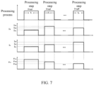
FIG. 7 illustrates a schematic diagram showing power compensation coefficients corresponding to different processing steps according to embodiments of the present disclosure. -
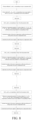
FIG. 8 illustrates a schematic block diagram of a power control method of a lower electrode RF power supply in the semiconductor processing equipment according to some embodiments of the present disclosure. -
FIG. 9 illustrates a schematic block diagram showing a principle of a power control device of the lower electrode RF power supply in the semiconductor processing equipment according to some embodiments of the present disclosure. -
FIG. 10 illustrates a schematic block diagram showing another principle of a power control device of the lower electrode RF power supply in the semiconductor processing equipment according to some embodiments of the present disclosure. - To help those skilled in the art better understand the technical solution of the present disclosure, a power control method and a power control device of lower radio frequency (RF) power supply in semiconductor processing equipment and the semiconductor processing equipment are described in detail below in conjunction with the accompanying drawings.
-
FIG. 1 illustrates a schematic structural diagram of an inductively coupled plasma equipment. As shown inFIG. 1 , the equipment includes aprocessing chamber 11. Adielectric window 6 is arranged at the top of the processing chamber. Aninductive coupling coil 5 is arranged above thedielectric window 6. Theinductive coupling coil 5 is electrically connected to an upperRF power supply 1 via anupper matcher 2. The upperRF power supply 1 can apply RF power onto theinductive coupling coil 5 via theupper matcher 2 to excite a process gas in theprocessing chamber 11 to form aplasma 9. Additionally, a lower electrode 8 (e.g., an electrostatic chuck) is arranged in processingchamber 11 and is configured to carry awafer 7. Thelower electrode 8 is electrically connected to a lowerRF power supply 4 via alower matcher 3. The lowerRF power supply 4 is configured to apply RF power onto thelower electrode 8 to generate an RF bias voltage on the wafer surface to accelerate ions to etch thewafer 7. - When the RF power of the lower
RF power supply 4 is applied to theelectrostatic chuck 8, a corresponding RF bias voltage is formed on thewafer 7. The RF bias voltage can be used to accelerate the ions to perform an etching process. When the applied RF power is different, the magnitude of the bias voltage on thewafer 7 can change, and the final etching process result can change. Thus, the overall efficiency consistency of the lower electrode circuit can be closely related to the process results. -
FIG. 2A illustrates a schematic diagram showing radio frequency (RF) power loss in a lower electrode RF circuit inFIG. 1 . As shown inFIG. 2A , the power loss during the process from the RF power output from the lowerRF power supply 4 to the power utilized by theplasma 9 mainly includes losses in the matcher, losses in the lower electrode to ground capacitance, losses in circuit contact, etc. In some embodiments, if the output power of the lowerRF power supply 4 is Pin, the total power loss of the lower electrode RF circuit can be P0, and the remaining power utilized by theplasma 9 can be Pp, Pp = Pin - P0. Then, the power transmission efficiency of the lower electrode RF circuit can be η, η = Pp / Pin. -
FIG. 2B illustrates an equivalent circuit diagram of the lower electrode RF circuit inFIG. 1 . As shown inFIG. 2B , capacitor C1 and capacitor C2 are variable capacitors inlower matcher 3. A loss resistance of thelower matcher 3 and a contact resistance of the lower electrode RF circuit as a whole can be considered as a loss equivalent resistance Rm of the lower electrode RF circuit. The loss equivalent resistance Rm is connected in series in the main path of the lower electrode RF circuit. Moreover, an equivalent circuit connected to an output end of the main path can include two parallel branches. One of the branches can be a lower electrode-to-ground branch. The lower electrode-to-ground branch can include a lower electrode-to-ground capacitance C and an equivalent resistance Rg when the lower electrode is grounded. The other branch can be a plasma sheath branch. The plasma sheath branch can include an impedance real part Rp and an equivalent inductance Lp of an impedance imaginary part of theplasma 9, and an impedance real part Rs and an equivalent capacitance Cs of an impedance imaginary part of the plasma sheath. Additionally, the current in the lower electrode-to-ground branch can be Ic, the current in the plasma sheath branch can be Is, and the current at the output end of thelower matcher 3 in the main path of the lower electrode RF circuit can be I. The current I can be equal to the sum of the currents Ic and Is. - Since among different chambers, the matcher in the lower electrode RF circuit, the lower electrode, the installation contact resistance, etc., are different, the equivalent resistance and capacitance of the parts of the lower electrode RF circuit can be different among different chambers. That is, the total power loss P0 in the lower electrode RF circuit can be different. Thus, among different chambers, when the output power Pin of the lower RF power supply is the same, and the total power loss P0 is different, the remaining power Pp utilized by the plasma 9 (the power transmission efficiency η) can be different. Then, the RF bias voltage generated on the wafer surface can be different, which affects the consistency of the processing results.
- To address the above problem,
FIG. 3 illustrates a schematic block diagram of a power control method of a lower RF power supply in semiconductor processing equipment according to embodiments of the present disclosure. The method includes the following steps. - At 101, when semiconductor processing begins in the processing chamber, with predetermined power compensation equation, and according to a pre-obtained first RF circuit parameter set of a reference chamber and a second RF circuit parameter set of a present processing chamber in which the semiconductor process is performed, a power compensation coefficient of the present processing chamber is obtained relative to the reference chamber.
- The reference chamber above can be one chamber specified from a plurality of chambers with the same structure. The first RF circuit parameter set of the reference chamber can refer to a combination of feature parameters of the lower electrode of the reference chamber. This first RF circuit parameter set can include but is not limited to the current at the output end of the
lower matcher 3 in the main path of the lower electrode RF circuit, the current in the plasma sheath branch of the lower electrode RF circuit, the loss equivalent resistance and the ground equivalent resistance of the lower electrode RF circuit, and the lower electrode-to-ground capacitance. - The present processing chamber above can be other processing chambers with the same structure except the reference chamber. When processing is performed in other process chambers, compensation can be performed on the output power of the lower
RF power supply 4 according to the inherent parameter of the processing chambers (i.e., the second RF circuit parameter set) and in connection with the inherent parameter and the plasma sheath parameter of the reference chamber (i.e., the first RF circuit parameter set) to achieve that the RF bias voltage generated on the wafer surface when the processing is performed in the other processing chambers with the same structure is consistent with the reference chamber. The second RF circuit parameter set of the present processing chamber can include but is not limited to the loss equivalent resistance and the grounded equivalent resistance of the lower RF circuit and the lower electrode-to-ground capacitance. - It should be noted that whether for the reference chamber or other process chambers, the inherent parameters such as the loss equivalent resistance Rm, the grounded equivalent resistance Rg, and the lower electrode-to-ground capacitance C can remain unchanged when performing the processing. The plasma sheath parameter of the lower electrode RF circuit (e.g., the RF bias voltage and the current in the plasma sheath branch) can change with different processing processes. The current Ic in the lower electrode-to-ground branch is made of most of the current I (usually greater than 10 amperes). However, the current Is in the plasma sheath branch can be small (smaller than 1 ampere). Thus, the current Is in the plasma sheath branch can be regarded as a constant current. Since the remaining power Pp utilized by the plasma 9 (also referred to as absorption power) is a product of the RF bias voltage and the current Is in the plasma sheath branch, the remaining power Pp can also change with the processing. Based on this, the lower electrode loss feature of different chambers can be reflected by the inherent parameters and the plasma sheath parameters. The difference in the remaining power Pp between the other processing chambers and the reference chamber can be compensated according to the lower electrode loss feature to allow different chambers to have the same remaining power Pp. Thus, the RF bias voltages of different chambers can be ensured to be consistent, and the processing results can be consistent.
- In some optional embodiments, as shown in
FIG. 4A , based on the inductively coupled plasma equipment shown inFIG. 1 , acurrent detection unit 24 is further arranged in the circuit between the output end of thelower matcher 3 and thelower electrode 8 and is configured to detect the current I at the output end of thelower matcher 3 in the main path of the lower electrode RF circuit. Additionally,voltage detection unit 23 is connected to thelower electrode 8 and is configured to detect the RF bias voltage on the wafer surface. Furthermore, a capacitance detection unit (not shown in the figure) can be connected to the lower electrode-to-ground branch and be configured to detect the lower electrode-to-ground capacitance C. - Taking the inductively coupled plasma equipment shown in
FIG. 4A as an example, as shown inFIG. 4B , corresponding to each processing chamber (including the reference chamber and other processing chambers), the following acquisition method can be used to obtain the loss equivalent resistance Rm and the grounded equivalent resistance Rg. - At 201, the lower
RF power supply 4 of the processing chamber (the upperRF power supply 1 is turned off) is turned on to apply a power setting value Plow on thelower electrode 8 via thelower matcher 3. - The power setting value Plow can be lower than the power value normally used in the processing. When the power setting value Plow is applied onto the
lower electrode 8, the determined power Plow can be almost fully consumed by the lower electrode-to-ground branch when thelower matcher 3 performs matching. Since the upperRF power supply 1 is turned off, and the power setting value Plow is low, the power may not be sufficient to cause the plasma in the processing chamber to ignite. Thus, no plasma load can be generated. - At 202, the current at the output end of the matcher (i.e., the lower matcher 3) in the main path of the lower electrode RF circuit, the present bias voltage value of the
lower electrode 8, and the lower electrode-to-ground capacitance are detected. - In step 202, the
current detection unit 24 can be configured to detect the current I0 at the output end of the matcher in the main path of the lower electrode RF circuit. Thevoltage detection unit 23 can be configured to detect the present bias voltage value V0 of thelower electrode 8, and the capacitance detection unit can be configured to detect the lower electrode-to-ground capacitance C. - In some embodiments, the equation (1) of the power setting value Plow is:

- The equation (2) of the present bias voltage value V0 of the
lower electrode 8 is:
- The following equations (3) and (4) are derived using the above equations (1) and (2).


- At 203, using the above equations (3) and (4), and according to the present current I0, the present bias voltage value V0, and lower electrode-to-ground capacitance C, the loss equivalent resistance Rm and the grounded equivalent resistance Rg of the lower electrode RF circuit are calculated.
- Of course, in practical applications, the loss equivalent resistance Rm and the grounded equivalent resistance Rg of the lower electrode RF circuit can also be obtained in any other methods, which are not limited in the present disclosure.
- Taking the inductively coupled plasma equipment shown in
FIG. 4A as an example of performingsemiconductor processing 1, as shown inFIG. 5A , the equation (5) of the bias voltage value V1 of thelower electrode 8 is:
semiconductor processing 1. - The equation (6) of the current I1 at the output end of the matcher in the main path of the lower electrode RF circuit corresponding to
semiconductor processing 1 is:
- The above bias voltage value V1 and current I1 can be detected and obtained by the
voltage detection unit 23 and thecurrent detection unit 24, respectively. The grounded equivalent resistance Rg can be calculated through the equation (3). Therefore, the equation (7) of the current Is1 in the plasma sheath branch corresponding tosemiconductor processing 1 is:
- For example,
semiconductor processing 2 is performed by the inductively coupled plasma equipment shown inFIG. 4A , as shown inFIG. 5B , the equation (8) of the bias voltage value V2 of thelower electrode 8 is:
semiconductor processing 2. - The equation (9) of the current I2 at the output end of the matcher in the main path of the lower electrode RF circuit corresponding to
semiconductor processing 2 is:
- The above bias voltage value V2 and current I2 can be detected by the
voltage detection unit 23 and thecurrent detection unit 24, respectively. The grounded equivalent resistance Rg can be calculated through the equation (3) as above. Therefore, the equation (10) of the current Is2 in the plasma sheath branch corresponding tosemiconductor processing 2 is:
- From the above, the equation for the current Is in the plasma sheath branch can be applied regardless of whether
semiconductor processing 1,semiconductor processing 2, or any other different processing. - Taking three process chambers (A, B, C) as an example, as shown in
FIG. 6 , firstly, step 201 to step 203 can be used to obtain the loss equivalent resistance RmA and grounded equivalent resistance RgA for processing chamber A, the loss equivalent resistance RmB and ground equivalent resistance RgB for processing chamber B, the loss equivalent resistance RmC and grounded equivalent resistance RgC for processing chamber C. Additionally, the capacitance detection unit of processing chamber A can be configured to obtain the lower electrode-to-ground capacitance CA. The capacitance detection unit of processing chamber B can be configured to obtain the lower electrode-to-ground capacitance CB. The capacitance detection unit of processing chamber C can be configured to obtain the lower electrode-to-ground capacitance Cc. - Since the loss equivalent resistances Rm, the grounded equivalent resistances Rg, and the lower electrode-to-ground capacitances C corresponding to different chambers are different, the bias voltage values corresponding to different chambers can be different. That is, for example,
semiconductor processing 1 is performed, VA1≠VB1≠VC1. Based on this, when the power setting value of the lowerelectrode power supply 4 of the three processing chambers (A, B, and C) is Pin, remaining power PpA, remaining power PpB, and remaining power PpC utilized by theplasma 9 corresponding to the three processing chambers (A, B, and C) can have the following equations.


semiconductor processing 1. - If processing chamber A is selected as the reference chamber, the equation (7) can be used to calculate the current Is1 for processing chamber A. The currents in the plasma sheath branches corresponding to
semiconductor processing 1 for the other two processing chambers (B and C) can be set to be equal to Is1. - When
semiconductor processing 1 is performed in processing chamber B, the power compensation coefficient of processing chamber B can be set to β B1 . If the remaining power PpB utilized by theplasma 9 corresponding to processing chamber B is equal to the remaining power PpC utilized by theplasma 9 corresponding to processing chamber C, the following equation exists.
- According to the equation (14) above, the equation for the power compensation coefficient β B1 for processing chamber B is derived as:

- Assuming that an RF frequency applied to the
lower electrode 8 is f, an impedance corresponding to the ground capacitance CA of processing chamber A is X, and


- Moreover, the currents at output ends of the matchers in the main paths of the lower RF circuits corresponding to processing chamber A and processing chamber B with the same power setting value Pin, respectively, are:


- Then, the power setting value Pin is:

- According to the above equations (16) to (20), the current IcB1 in the lower electrode-to-ground branch corresponding to processing chamber B is derived as:

- Using processing chamber A as the reference chamber, and substituting the above equation (21) into the equation (15), the power compensation equation for processing chamber B corresponding to
semiconductor processing 1 is derived as:
- Where, β B1 is the power compensation coefficient for processing chamber B corresponding to
semiconductor processing 1 relative to processing chamber A. - The first RF circuit parameter set of processing chamber A can include IA, IS, RmA, RgA, and X. IA1 is the current at the output end of the matcher in the main path of the lower electrode RF circuit corresponding to
semiconductor processing 1. Is1 is the current in the plasma sheath circuit branch of the lower electrode RF circuit corresponding tosemiconductor processing 1. RmA is the loss equivalent resistance of the lower electrode RF circuit of processing chamber A. RgA is the grounded equivalent resistance of the lower electrode RF circuit of processing chamber A. X is the impedance value corresponding to the lower electrode-to-ground capacitance of processing chamber A, and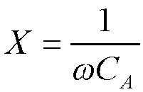
- The second RF circuit parameter set of processing chamber B can include RmB, RgB, and Y. RmB is the loss equivalent resistance of the lower electrode RF circuit of processing chamber B. RgB is the grounded equivalent resistance of the lower electrode RF circuit of processing chamber B. Y is the impedance value corresponding to the lower electrode-to-ground capacitance of processing chamber B, and

- Similarly, using processing chamber A as the reference chamber, the power compensation equation for processing chamber C corresponding to
semiconductor processing 1 is derived as:
- Where β C1 is the power compensation coefficient for processing chamber C corresponding to
semiconductor processing 1 relative to processing chamber A. - The second RF circuit parameter set of processing chamber C can include RmC, RgC, and Z. RmC is the loss equivalent resistance of the lower electrode RF circuit of processing chamber C. RgC is the grounded equivalent resistance of the lower electrode RF circuit of processing chamber C. Z is the impedance value corresponding to the lower electrode-to-ground capacitance of processing chamber C, and

- Similarly, using processing chamber A as the reference chamber, the power compensation equations for processing chamber B and processing chamber C corresponding to semiconductor processing 2 are derived as:


- It should be noted that the
semiconductor processing 1 andsemiconductor processing 2 above can include two different processing recipes or two different processing steps within the same semiconductor processing. - In some optional embodiments, the semiconductor processing can include a plurality of processing steps. For different processing steps, the current Is1 in the plasma sheath branch of the lower RF circuit can be different. Thus, taking processing chamber A as the reference chamber as an example, the power control method of embodiments of the present disclosure further includes the following steps.
- At 301, before performing the semiconductor processing, pre-obtained IA (the current at the output end of the
lower matcher 3 in the main path of the lower RF circuit) and IS (the current in the plasma sheath branch) corresponding to the processing steps are written in a parameter table. For example, the processing steps include N steps, and N is an integer greater than 1. - The IA and IS corresponding to the processing steps can be calculated using the equation (7) above.
Table 1 shows the parameter table of IA and IS of processing chamber A (i.e., the reference chamber) corresponding to the N processing steps. Step Is IA 1 Is1 IA1 2 Is2 IA2 ... ... ... N IsN IAN - At 302, the pre-obtained RmA, RgA, and CA corresponding to processing chamber A and RmB, RgB, and CB corresponding to processing chamber B are called.
- Then, step 101 is performed. Step 101 can include:
- when processing chamber B begins an i-th processing step (i=1, 2, ..., N), calling IAi and ISi corresponding to the i-th processing step from the parameter table; and
- by using the power compensation equation (22) and according to IAi, ISi, RmA, RgA, CA, RmB, RgB, and CB corresponding to the i-th processing step, obtaining the power compensation coefficient βBi of processing chamber B corresponding to the i-th processing step.
- As shown in
FIG. 7 , in a process of performing N processing steps (Step1, Step2, ..., StepN), each processing step corresponds to an Is, an IA, and a power compensation coefficient. - It should be noted that the method for obtaining the power compensation coefficient βBi corresponding to the i-th processing step is illustrated here only with processing chamber B as an example. In practical applications, the other chambers with the same structure except the reference chamber can be suitable for the method for obtaining the power compensation coefficient βi corresponding to the i-th processing step.
- At 102, the power compensation value of the present processing chamber relative to the reference chamber is calculated according to the power compensation coefficient and the power setting value of the lower RF power supply of the present processing chamber.
- In some optional embodiments, step 102 can specifically include:
calculating the product of the power compensation coefficient and the power setting value as the power compensation value. - At 103, the lower
RF power supply 4 is controlled to output the power compensation value. - In
step 103, the power output by the lowerRF power supply 4 can be the compensated power value. - For the plurality of processing steps, each
time step 103 is performed until the current processing step ends, and a next processing step is performed, IA and IS corresponding to the next processing step can be called from the parameter table, and the power compensation coefficient corresponding to the next processing step can be calculated again. For the specific execution processes, reference can be made toFIG. 8 . - Step 102 and step 103 are used to calculate the power compensation value and perform power compensation on the power setting value (i.e., Pin) output by the lower
RF power supply 4. Thus, the remaining power PP utilized by theplasma 9 of the other chambers with the same structure except the reference chamber can be consistent with the remaining power PP of the reference chamber to ensure that the RF bias voltages of different chambers are consistent to achieve consistent processing results. - As another technical solution, as shown in
FIG. 9 , embodiments of the present disclosure also provide apower control device 20 of the lower RF power supply in the semiconductor processing equipment, which includes acalculation unit 21 and acontrol unit 22. Thecalculation unit 21 can be configured to, when the semiconductor processing begins in the processing chamber, obtain the power compensation coefficient of the present processing chamber relative to the reference chamber by using the predetermined power compensation equation and according to the pre-obtained first RF circuit parameter set of the reference chamber and the second RF circuit parameter set of the present processing chamber that performs the semiconductor processing, and calculate the power compensation value of the present processing chamber relative to the reference chamber according to the power compensation coefficient and the power setting value of the lower RF power supply of the present processing chamber. - The
control unit 22 can be configured to control the lower RF power supply to output the power compensation value. - The reference chamber can be a determined chamber from the plurality of processing chambers with the same structure. The first RF circuit parameter set of the reference chamber can be a combination of the feature parameters of the lower electrode of the reference chamber. The first RF circuit parameter set can include but is not limited to the current at the output end of the lower matcher in the main path of the lower electrode RF circuit, the current of the plasma sheath branch of the lower electrode RF circuit, the loss equivalent resistance and the grounded equivalent resistance of the lower electrode RF circuit, and the lower electrode-to-ground capacitance.
- The present processing chamber can be processing chambers with the same structure except the reference chamber. The second RF circuit parameter set of the present processing chamber can include but is not limited to the loss equivalent resistance and the grounded equivalent resistance of the lower RF circuit and the lower electrode-to-ground capacitance.
- Taking the inductively coupled plasma equipment shown in
FIG. 4A as an example, as shown inFIG. 2B , capacitor C1 and capacitor C2 are both variable capacitors in thelower matcher 3. The loss resistance of thelower matcher 3 and the contact resistance of the lower electrode RF circuit as a whole can be considered as the loss equivalent resistance Rm of the lower electrode RF circuit. The loss equivalent resistance Rm can be connected in series in the main path of the lower electrode RF circuit. The equivalent circuit part connected to the output end of the main path can include two parallel branches. One of the branches can be a lower electrode-to-ground branch. The lower electrode-to-ground branch can include a lower electrode-to-ground capacitance C and an equivalent resistance Rg when the lower electrode is grounded. The other branch can be a plasma sheath branch. The plasma sheath branch can include an equivalent inductance Lp of an impedance real part Rp and an impedance imaginary part of theplasma 9, and an equivalent capacitance Cs of an impedance real part Rs and an impedance imaginary part of the plasma sheathr. Additionally, the current in the lower electrode-to-ground branch can be Ic, the current in the plasma sheath branch can be Is, and the current at the output end of thelower matcher 3 in the main path of the lower electrode RF circuit can be I. - It should be noted that whether for the reference chamber or other process chambers, the inherent parameters such as the loss equivalent resistance Rm, the grounded equivalent resistance Rg, and the lower electrode-to-ground capacitance C can remain unchanged when performing the processing. The plasma sheath parameter of the lower electrode RF circuit (e.g., the RF bias voltage and the current in the plasma sheath branch) can change with different processing processes. The current Ic in the lower electrode-to-ground branch is made of most of the current I (usually greater than 10 amperes). However, the current Is in the plasma sheath branch can be small (smaller than 1 ampere). Thus, the current Is in the plasma sheath branch can be regarded as a constant current. Since the remaining power Pp utilized by the plasma 9 (also referred to as absorption power) is a product of the RF bias voltage and the current Is in the plasma sheath branch, the remaining power Pp can also change with the processing. Based on this, the lower electrode loss feature of different chambers can be reflected by the inherent parameters and the plasma sheath parameters. The difference in the remaining power Pp between the other processing chambers and the reference chamber can be compensated according to the lower electrode loss feature to allow different chambers to have the same remaining power Pp. Thus, the RF bias voltages of different chambers can be ensured to be consistent, and the processing results can be consistent.
- In some optional embodiments, the above power compensation equation is:

- Where βB is the power compensation coefficient of the present processing chamber (taking the processing chamber B in
FIG. 6 as an example) relative to the reference chamber. The first RF circuit parameter set can include IA, IS, RmA, RgA, and X, where IA is the current at the output end of the matcher in the main path of the lower electrode RF circuit. IS is the current in the plasma sheath branch of the lower electrode RF circuit of the reference chamber. RmA is the loss equivalent resistance of the lower electrode RF circuit of the reference chamber; RgA is the grounded equivalent resistance of the lower electrode RF circuit of the reference chamber. X is the impedance value corresponding to the lower electrode-to-ground capacitance of the reference chamber, and
- The second RF circuit parameter set can include RmB, RgB, and Y. RmB is the loss equivalent resistance of the lower electrode RF circuit of the present processing chamber. RgB is the grounded equivalent resistance of the lower electrode RF circuit of the present processing chamber. Y is the impedance value corresponding to the lower electrode-to-ground capacitance of the present processing chamber.

- In some optional embodiments, taking the inductively coupled plasma equipment shown in
FIG. 4A as an example, thecontrol unit 22 is also configured to activate the lowerRF power supply 4 of the processing chamber and apply the determined power value to thelower electrode 8 through thematcher 3 to ensure that the plasma in the processing chamber does not ignite. - Specifically, as shown in
FIG. 4B , corresponding to each processing chamber (including the reference chamber and the processing chamber), the lowerRF power supply 4 of the processing chamber is activated (the upperRF power supply 1 is turned off). The determined power value Plow is applied to thelower electrode 8 throughmatcher 3. - The determined power value Plow can be low compared to the power value adopted by normal processing. Thus, when the determined power value Plow is applied to the lower electrode, when the
lower matcher 3 is paired, the determined power value Plow can be consumed by the lower electrode-to-ground branch. Since theRF power supply 1 is turned off, and the determined power value Plow is low, the power may not be sufficient to cause the plasma in the processing chamber to ignite. Thus, the plasma load cannot be generated. - Based on this, as shown in
FIG. 10 , thepower control device 20 further includes acurrent detection unit 24, avoltage detection unit 23, and acapacitance detection unit 25. Thecurrent detection unit 24 is arranged in the circuit between the output end of thematcher 3 and thelower electrode 8 and configured to detect the present current (i.e., I0) at the output end side of thelower matcher 3 in the main path of the lower electrode RF circuit. The voltage detection unit, for example, can be electrically connected to the RF electrode of thelower electrode 8 and configured to detect the present bias voltage value of the lower electrode 8 (i.e., V0). The capacitance detection unit can be configured to detect the lower electrode-to-ground capacitance (i.e., C) of thelower electrode 8. - Based on this, the
calculation unit 21 can be further configured to calculate the loss equivalent resistance Rm and the grounded equivalent resistance Rg of the lower electrode RF circuit using the following equation and the present current I0, the present bias voltage value V0, and the lower electrode-to-ground capacitance C. The equations are as follows.

- In some optional embodiments, the semiconductor processing can include a plurality of processing steps. The
power control device 20 can further include a writing unit. The writing unit can be configured to write the pre-obtained IA (the current at the output end side of thelower matcher 3 in the main path of the lower electrode RF circuit) and IS (the current in the plasma sheath branch) into the parameter table. - Optionally, IA and Is corresponding to the processing steps (Step) can be calculated through the equation (7) of the above embodiments.
- Based on this, taking processing chamber A as the reference chamber and processing chamber B as the chamber that is performing the processing as an example, the
calculation unit 21 can be further configured to call RmA, RgA, CA, RmB, RgB, and CB. When processing chamber B starts to perform the i-th processing step (i = 1, 2, ..., N), IAi and ISi corresponding to the i-th processing step can be called from the above parameter table. With the above power compensation equation, and according to IAi, ISi, RmA, RgA, CA, RmB, RgB, and CB corresponding to the i-th processing step, the power compensation coefficient βBi of processing chamber B corresponding to the i-th processing step. - In some optional embodiments, the
calculation unit 21 can be configured to calculate the product of the power compensation coefficient and the power setting value as the power compensation value. - In the technical solution of the power control method and device of the lower RF power supply in the semiconductor processing equipment of embodiments of the present disclosure, when the processing chamber starts the semiconductor processing, with the pre-determined power compensation equation and according to the pre-obtained first RF circuit parameter set and the second RF circuit parameter set of the present processing chamber performing the semiconductor processing, the power compensation coefficient can be obtained. According to the power compensation coefficient and the power setting value of the lower RF power supply of the present processing chamber, the power compensation value can be calculated. Then, the lower RF power supply can be controlled to output the power compensation value. Thus, the difference in the power utilized by the plasma between the other processing chambers except for the reference chamber and the reference chamber can be compensated. Thus, the consistency in the bias voltage values generated on the wafers between different chambers under the same processing recipe can be improved. Thus, the processing result consistency of the different processing chambers can be improved.
- As another technical solution, embodiments of the present disclosure further provide semiconductor processing equipment. Taking the inductively coupled plasma equipment shown in FIG. A as an example, the equipment includes processing
chamber 11. Adielectric window 6 is arranged at the top of processingchamber 11. Aninductive coupling coil 5 is arranged above thedielectric window 6. Theinductive coupling coil 5 can be electrically connected to the upperRF power supply 1 through theupper matcher 2. The upperRF power supply 1 can apply the RF power to theinductive coupling coil 5 through theupper matcher 2 to excite the process gas in theprocessing chamber 11 to generate theplasma 9. Moreover, the lower electrode 8 (e.g., the electrostatic chuck) can be arranged in theprocessing chamber 11 and configured to carry thewafer 7. Thelower electrode 8 can be electrically connected to the lowerRF power supply 4 through thelower matcher 3. The lowerRF power supply 4 can be configured to apply the RF power to thelower electrode 8 to generate the RF bias voltage on the wafer surface to accelerate the ions to etch the wafer. - The semiconductor processing equipment of embodiments of the present disclosure can adopt the power control device of embodiments of the present disclosure. With the device, the consistency in the bias voltage values generated on the wafers of different chambers under the same processing recipe can be improved. Thus, the processing result consistency of the different processing chambers can be improved.
- It can be noted that the above embodiments are merely exemplary embodiments used to illustrate the principle of the present disclosure. However, the present disclosure is not limited to this. For those skilled in the art, without departing from the spirit and essence of the present disclosure, various variations and improvements can be made. These variations and improvements are also within the scope of the present disclosure.
Claims (11)
- A power control method of a lower RF power supply of semiconductor processing equipment comprising:when a processing chamber starts semiconductor processing, with a predetermined power compensation equation and according to a pre-obtained first RF circuit parameter set of a reference chamber and a second RF circuit parameter set of a present processing chamber performing the semiconductor processing, obtaining a power compensation coefficient of the present processing chamber relative to the reference chamber;according to the power compensation coefficient and a power setting value of the lower RF power supply of the present processing chamber, calculating a power compensation value of the present processing chamber relative to the reference chamber; andcontrolling the lower RF power supply to output the power compensation value.
- The power control method according to claim 1, wherein a power compensation equation is:
 βB is the power compensation coefficient of the present processing chamber relative to the reference chamber;the first RF circuit parameter set includes IA, IS, RmA, RgA, and X;IA is a current at an output end of a matcher in a main path of a lower electrode RF circuit of the reference chamber;IS is a current in a plasma sheath branch of the lower electrode RF circuit of the reference chamber;RmA is a loss equivalent resistance of the lower electrode RF circuit of the reference chamber;RgA is a grounded equivalent resistance of the lower electrode RF circuit of the reference chamber;X is an impedance value corresponding to a lower electrode-to-ground capacitance of the reference chamber, and
 the second RF circuit parameter set includes RmB, RgB, and Y;RmB is a loss equivalent resistance of a lower electrode RF circuit of the present processing chamber;RgB is a grounded equivalent resistance of the lower electrode RF circuit of the present processing chamber;Y is an impedance value corresponding to a lower electrode-to-ground capacitance of the present processing chamber, and
- The power control method according to claim 2, wherein acquisition methods of the loss equivalent resistance and the grounded equivalent resistance of the lower electrode RF circuit for each processing chamber include:turning on the lower RF power supply of the processing chamber to apply a determined power value to the lower electrode through the matcher to ensure that a plasma in the processing chamber does not ignite;detecting a present current at an output end of the matcher in a main path in the lower electrode RF circuit, a present bias voltage value of the lower electrode, and a lower electrode-to-ground capacitance; andusing following equations to calculate the loss equivalent resistance and the grounded equivalent resistance of the lower electrode RF circuit according to the present current, the present bias voltage value, and the lower electrode-to-ground capacitance:

 wherein:Rg is the grounded equivalent resistance of the lower electrode RF circuit;Rm is the loss equivalent resistance of the lower electrode RF circuit;V0 is the present bias voltage value;I0 is the present current;ω is the angular frequency;C is the lower electrode-to-ground capacitance; andPlow is the determined power value.
 - The power control method according to claim 2, wherein the semiconductor processing includes a plurality of processing steps;
the power control method further comprising:before performing the semiconductor processing, writing pre-obtained IA and IS corresponding to the processing steps into a parameter table;calling RmA, RgA, CA, RmB, RgB, and CB; andwhen the processing chamber starts performing the semiconductor processing, with the predetermined power compensation equation and according to the pre-obtained first RF circuit parameter set of the reference chamber and the second RF circuit parameter set of the present processing chamber performing the semiconductor processing, obtaining the power compensation coefficient of the present processing chamber relative to the reference chamber, including:when the present processing chamber starts performing the processing steps, calling IA and IS corresponding to a current processing step from the parameter table; andwith the power compensation equation and according to IA, IS, RmA, RgA, CA, RmB, RgB, and CB, obtaining the power compensation coefficient. - The power control method according to claim 1, wherein according to the power compensation coefficient and the power setting value of the lower RF power supply of the present processing chamber, obtaining the power compensation value of the present processing chamber relative to the reference chamber includes:
calculating a product of the power compensation coefficient and the power setting value as the power compensation value. - A power control device of a lower RF power supply in semiconductor process equipment comprising a calculation unit and a control unit, wherein:the calculation unit is configured to, when a processing chamber starts semiconductor processing, adopt a predetermined power compensation equation, a pre-obtained first RF circuit parameter set of a reference chamber, and a second RF circuit parameter set of a present processing chamber performing the semiconductor processing, obtain a power compensation coefficient of the present processing chamber relative to the reference chamber, and according to the power compensation coefficient and a power setting value of the lower RF power supply of the present processing chamber, and calculate a power compensation value of the present processing chamber relative to the reference chamber; andthe control unit is configured to control the lower RF power supply to output the power compensation value.
- The power control device according to claim 6, wherein the power compensation equation is:
 βB is the power compensation coefficient of the present processing chamber relative to the reference chamber;the first RF circuit parameter set includes IA, IS, RmA, RgA, and X;IA is a current at an output end of a matcher in a main path of a lower electrode RF circuit;IS is a current in a plasma sheath branch of the lower electrode RF circuit of the reference chamber;RmA is a loss equivalent resistance of the lower electrode RF circuit of the reference chamber;RgA is a grounded equivalent resistance of the lower electrode RF circuit of the reference chamber;X is an impedance value corresponding to a lower electrode-to-ground capacitance of the reference chamber, and
 the second RF circuit parameter set includes RmB, RgB, and Y;RmB is a loss equivalent resistance of a lower electrode RF circuit of the present processing chamber;RgB is a grounded equivalent resistance of the lower electrode RF circuit of the present processing chamber;Y is an impedance value corresponding to a lower electrode-to-ground capacitance of the present processing chamber, and
- The power control device according to claim 6, wherein the control unit is further configured to turn on the lower RF power supply of the processing chamber to apply a determined power value to the lower electrode through the matcher to ensure that a plasma in the processing chamber does not ignite;the power control device further comprising a current detection unit, a voltage detection unit, and a capacitance detection unit, wherein the current detection unit is configured to detect a present current at an output end of the matcher in a main path in the lower electrode RF circuit, a present bias voltage value of the lower electrode;the voltage detection unit is configured to detect the present bias voltage value of the lower electrode;the capacitance detection unit is configured to detect a lower electrode-to-ground capacitance; andthe calculation unit is further configured to use following equations to calculate the loss equivalent resistance and the grounded equivalent resistance of the lower electrode RF circuit according to the present current, the present bias voltage value, and the lower electrode-to-ground capacitance:wherein:

 Rg is the grounded equivalent resistance of the lower electrode RF circuit;Rm is the loss equivalent resistance of the lower electrode RF circuit;V0 is the present bias voltage value;I0 is the present current;ω is the angular frequency;C is the lower electrode-to-ground capacitance; andPlow is the determined power value.
 - The power control device according to claim 7, wherein the semiconductor processing includes a plurality of processing steps;the power control device further comprising a writing unit, the writing unit is configured to, before performing the semiconductor processing, write pre-obtained IA and IS corresponding to the processing steps into a parameter table; andthe calculation unit is further configured to call RmA, RgA, CA, RmB, RgB, and CB, when the present processing chamber starts performing the processing steps, call IA and IS corresponding to a current processing step from the parameter table, and with the power compensation equation and according to IA, IS, RmA, RgA, CA, RmB, RgB, and CB, obtain the power compensation coefficient.
- The power control device according to claim 6, wherein the calculation unit is configured to calculate a product of the power compensation coefficient and the power setting value as the power compensation value.
- Semiconductor processing equipment comprising a processing chamber, a matcher, and a lower RF power supply, wherein a lower electrode is arranged in the processing chamber, the lower electrode is electrically connected to the lower RF power supply through the matcher, and the semiconductor processing equipment further includes the power control device of any one of claims 6 to 10.
Applications Claiming Priority (2)
| Application Number | Priority Date | Filing Date | Title |
|---|---|---|---|
| CN202111126996.7A CN113903643B (en) | 2021-09-26 | 2021-09-26 | Power control method and device of radio frequency power supply, semiconductor process equipment |
| PCT/CN2022/120101 WO2023045944A1 (en) | 2021-09-26 | 2022-09-21 | Power control method and apparatus for lower radio frequency power source, and semiconductor processing device |
Publications (2)
| Publication Number | Publication Date |
|---|---|
| EP4407651A1 true EP4407651A1 (en) | 2024-07-31 |
| EP4407651A4 EP4407651A4 (en) | 2025-06-25 |
Family
ID=79029194
Family Applications (1)
| Application Number | Title | Priority Date | Filing Date |
|---|---|---|---|
| EP22871990.2A Pending EP4407651A4 (en) | 2021-09-26 | 2022-09-21 | Power control method and apparatus for a low-frequency power source and semiconductor processing device |
Country Status (6)
| Country | Link |
|---|---|
| US (1) | US12394593B2 (en) |
| EP (1) | EP4407651A4 (en) |
| KR (1) | KR102934519B1 (en) |
| CN (1) | CN113903643B (en) |
| TW (1) | TWI853309B (en) |
| WO (1) | WO2023045944A1 (en) |
Families Citing this family (2)
| Publication number | Priority date | Publication date | Assignee | Title |
|---|---|---|---|---|
| CN113903643B (en) * | 2021-09-26 | 2024-07-23 | 北京北方华创微电子装备有限公司 | Power control method and device of radio frequency power supply, semiconductor process equipment |
| CN119920726B (en) * | 2024-12-11 | 2025-11-07 | 北京吉兆源科技有限公司 | RF power supply output power calibration method and apparatus, semiconductor process method |
Family Cites Families (19)
| Publication number | Priority date | Publication date | Assignee | Title |
|---|---|---|---|---|
| JP3364675B2 (en) * | 1997-09-30 | 2003-01-08 | 東京エレクトロンエイ・ティー株式会社 | Plasma processing equipment |
| US7794615B2 (en) * | 2005-03-31 | 2010-09-14 | Tokyo Electron Limited | Plasma processing method and apparatus, and autorunning program for variable matching unit |
| JP4350766B2 (en) * | 2007-03-30 | 2009-10-21 | 東京エレクトロン株式会社 | Plasma processing equipment, high frequency power supply calibration method, high frequency power supply |
| CN101996840B (en) * | 2009-08-10 | 2013-02-06 | 北京北方微电子基地设备工艺研究中心有限责任公司 | Plasma processing equipment and method and method for washing chamber |
| US9412670B2 (en) * | 2013-05-23 | 2016-08-09 | Lam Research Corporation | System, method and apparatus for RF power compensation in plasma etch chamber |
| CN104281185B (en) * | 2013-07-12 | 2016-04-20 | 北京北方微电子基地设备工艺研究中心有限责任公司 | Rf control system and method, reaction chamber, plasma processing device |
| US9508529B2 (en) * | 2014-10-23 | 2016-11-29 | Lam Research Corporation | System, method and apparatus for RF power compensation in a plasma processing system |
| CN106328550A (en) * | 2015-07-01 | 2017-01-11 | 北京北方微电子基地设备工艺研究中心有限责任公司 | Process method and device |
| KR102415329B1 (en) * | 2015-09-08 | 2022-06-30 | 삼성전자주식회사 | Tube-type lens, OES(Optical Emission Spectroscopy) apparatus comprising the tube-type lens, plasma monitoring system comprising the OES apparatus, and method for fabricating semiconductor device using the system |
| KR102334378B1 (en) * | 2015-09-23 | 2021-12-02 | 삼성전자 주식회사 | Dielectric window, plasma processing system comprising the window, and method for fabricating semiconductor device using the system |
| US10622217B2 (en) * | 2016-02-04 | 2020-04-14 | Samsung Electronics Co., Ltd. | Method of plasma etching and method of fabricating semiconductor device using the same |
| KR20190055607A (en) * | 2017-11-15 | 2019-05-23 | 삼성전자주식회사 | Plasma processing apparatus |
| US12002653B2 (en) * | 2019-06-20 | 2024-06-04 | Lam Research Corporation | Systems and methods for compensating for RF power loss |
| CN110299279B (en) * | 2019-08-22 | 2019-11-12 | 中微半导体设备(上海)股份有限公司 | A radio frequency power supply system, plasma processor and frequency modulation matching method thereof |
| JP7257918B2 (en) * | 2019-08-29 | 2023-04-14 | 東京エレクトロン株式会社 | Plasma processing system and plasma ignition support method |
| JP7374023B2 (en) * | 2020-03-09 | 2023-11-06 | 東京エレクトロン株式会社 | Inspection method and plasma processing equipment |
| CN113113282B (en) * | 2021-04-01 | 2023-11-14 | 北京北方华创微电子装备有限公司 | Upper electrode power supply power adjustment method, semiconductor process equipment |
| US11961712B2 (en) * | 2021-04-26 | 2024-04-16 | Advanced Energy Industries, Inc. | Combining the determination of single and mutual, preset preserving, impedance loads with advances in single and double sensor calibration techniques in the application of single and pairwise calibration of sensors |
| CN113903643B (en) * | 2021-09-26 | 2024-07-23 | 北京北方华创微电子装备有限公司 | Power control method and device of radio frequency power supply, semiconductor process equipment |
-
2021
- 2021-09-26 CN CN202111126996.7A patent/CN113903643B/en active Active
-
2022
- 2022-09-21 WO PCT/CN2022/120101 patent/WO2023045944A1/en not_active Ceased
- 2022-09-21 EP EP22871990.2A patent/EP4407651A4/en active Pending
- 2022-09-21 KR KR1020247009956A patent/KR102934519B1/en active Active
- 2022-09-21 TW TW111135795A patent/TWI853309B/en active
-
2024
- 2024-03-26 US US18/616,998 patent/US12394593B2/en active Active
Also Published As
| Publication number | Publication date |
|---|---|
| CN113903643A (en) | 2022-01-07 |
| TW202315465A (en) | 2023-04-01 |
| US20240234088A1 (en) | 2024-07-11 |
| WO2023045944A1 (en) | 2023-03-30 |
| EP4407651A4 (en) | 2025-06-25 |
| CN113903643B (en) | 2024-07-23 |
| TWI853309B (en) | 2024-08-21 |
| KR20240048547A (en) | 2024-04-15 |
| KR102934519B1 (en) | 2026-03-06 |
| WO2023045944A9 (en) | 2024-03-21 |
| US12394593B2 (en) | 2025-08-19 |
Similar Documents
| Publication | Publication Date | Title |
|---|---|---|
| US12394593B2 (en) | Power control method and device of lower radio frequency power supply and semiconductor processing equipment | |
| US12040770B2 (en) | Multiple-output radiofrequency matching module and associated methods | |
| US6174450B1 (en) | Methods and apparatus for controlling ion energy and plasma density in a plasma processing system | |
| US6884635B2 (en) | Control of power delivered to a multiple segment inject electrode | |
| EP4318547A1 (en) | Upper electrode power supply power adjustment method, and semiconductor process device | |
| KR20140104380A (en) | Plasma processing apparatus and plasma processing method | |
| US20120000888A1 (en) | Methods and apparatus for radio frequency (rf) plasma processing | |
| KR102690539B1 (en) | Impedance matching method, impedance matcher, and semiconductor process device | |
| CN108122724A (en) | General non-intrusion type room impedance measurement system and correlation technique | |
| CN113066712B (en) | Impedance matching method and semiconductor process equipment | |
| CN107180737A (en) | Device and semiconductor processing equipment for realizing impedance matching and power distribution | |
| US20210398778A1 (en) | Methods and apparatus for processing a substrate | |
| KR20140051808A (en) | Tcct match circuit for plasma etch chambers | |
| KR102190926B1 (en) | System for measuring status of substrate and plasma | |
| US6954033B2 (en) | Plasma processing apparatus | |
| JPH05205898A (en) | Plasma processing device | |
| CN216648218U (en) | Radio frequency providing device and plasma processing equipment | |
| JP7318114B2 (en) | Tuning method for improving plasma stability | |
| US20240203691A1 (en) | Apparatus for processing substrates and method of processing substrates using the same | |
| CN115491657B (en) | Cleaning methods, storage media, drive circuits and semiconductor processing equipment | |
| CN120784146A (en) | Power control method of lower electrode assembly and semiconductor process equipment |
Legal Events
| Date | Code | Title | Description |
|---|---|---|---|
| STAA | Information on the status of an ep patent application or granted ep patent |
Free format text: STATUS: THE INTERNATIONAL PUBLICATION HAS BEEN MADE |
|
| PUAI | Public reference made under article 153(3) epc to a published international application that has entered the european phase |
Free format text: ORIGINAL CODE: 0009012 |
|
| STAA | Information on the status of an ep patent application or granted ep patent |
Free format text: STATUS: REQUEST FOR EXAMINATION WAS MADE |
|
| 17P | Request for examination filed |
Effective date: 20240326 |
|
| AK | Designated contracting states |
Kind code of ref document: A1 Designated state(s): AL AT BE BG CH CY CZ DE DK EE ES FI FR GB GR HR HU IE IS IT LI LT LU LV MC MK MT NL NO PL PT RO RS SE SI SK SM TR |
|
| DAV | Request for validation of the european patent (deleted) | ||
| DAX | Request for extension of the european patent (deleted) | ||
| A4 | Supplementary search report drawn up and despatched |
Effective date: 20250526 |
|
| RIC1 | Information provided on ipc code assigned before grant |
Ipc: H01J 37/32 20060101ALI20250520BHEP Ipc: H01J 7/24 20060101AFI20250520BHEP |