EP4407596A1 - Gate driving circuit and display device including the same - Google Patents
Gate driving circuit and display device including the same Download PDFInfo
- Publication number
- EP4407596A1 EP4407596A1 EP23208885.6A EP23208885A EP4407596A1 EP 4407596 A1 EP4407596 A1 EP 4407596A1 EP 23208885 A EP23208885 A EP 23208885A EP 4407596 A1 EP4407596 A1 EP 4407596A1
- Authority
- EP
- European Patent Office
- Prior art keywords
- transistor
- electrode
- node
- driving circuit
- signal
- Prior art date
- Legal status (The legal status is an assumption and is not a legal conclusion. Google has not performed a legal analysis and makes no representation as to the accuracy of the status listed.)
- Pending
Links
Images



Classifications
-
- G—PHYSICS
- G09—EDUCATION; CRYPTOGRAPHY; DISPLAY; ADVERTISING; SEALS
- G09G—ARRANGEMENTS OR CIRCUITS FOR CONTROL OF INDICATING DEVICES USING STATIC MEANS TO PRESENT VARIABLE INFORMATION
- G09G3/00—Control arrangements or circuits, of interest only in connection with visual indicators other than cathode-ray tubes
- G09G3/20—Control arrangements or circuits, of interest only in connection with visual indicators other than cathode-ray tubes for presentation of an assembly of a number of characters, e.g. a page, by composing the assembly by combination of individual elements arranged in a matrix no fixed position being assigned to or needed to be assigned to the individual characters or partial characters
- G09G3/2007—Display of intermediate tones
- G09G3/2074—Display of intermediate tones using sub-pixels
-
- G—PHYSICS
- G09—EDUCATION; CRYPTOGRAPHY; DISPLAY; ADVERTISING; SEALS
- G09G—ARRANGEMENTS OR CIRCUITS FOR CONTROL OF INDICATING DEVICES USING STATIC MEANS TO PRESENT VARIABLE INFORMATION
- G09G3/00—Control arrangements or circuits, of interest only in connection with visual indicators other than cathode-ray tubes
- G09G3/20—Control arrangements or circuits, of interest only in connection with visual indicators other than cathode-ray tubes for presentation of an assembly of a number of characters, e.g. a page, by composing the assembly by combination of individual elements arranged in a matrix no fixed position being assigned to or needed to be assigned to the individual characters or partial characters
- G09G3/22—Control arrangements or circuits, of interest only in connection with visual indicators other than cathode-ray tubes for presentation of an assembly of a number of characters, e.g. a page, by composing the assembly by combination of individual elements arranged in a matrix no fixed position being assigned to or needed to be assigned to the individual characters or partial characters using controlled light sources
- G09G3/30—Control arrangements or circuits, of interest only in connection with visual indicators other than cathode-ray tubes for presentation of an assembly of a number of characters, e.g. a page, by composing the assembly by combination of individual elements arranged in a matrix no fixed position being assigned to or needed to be assigned to the individual characters or partial characters using controlled light sources using electroluminescent panels
- G09G3/32—Control arrangements or circuits, of interest only in connection with visual indicators other than cathode-ray tubes for presentation of an assembly of a number of characters, e.g. a page, by composing the assembly by combination of individual elements arranged in a matrix no fixed position being assigned to or needed to be assigned to the individual characters or partial characters using controlled light sources using electroluminescent panels semiconductive, e.g. using light-emitting diodes [LED]
- G09G3/3208—Control arrangements or circuits, of interest only in connection with visual indicators other than cathode-ray tubes for presentation of an assembly of a number of characters, e.g. a page, by composing the assembly by combination of individual elements arranged in a matrix no fixed position being assigned to or needed to be assigned to the individual characters or partial characters using controlled light sources using electroluminescent panels semiconductive, e.g. using light-emitting diodes [LED] organic, e.g. using organic light-emitting diodes [OLED]
- G09G3/3266—Details of drivers for scan electrodes
-
- G—PHYSICS
- G06—COMPUTING OR CALCULATING; COUNTING
- G06F—ELECTRIC DIGITAL DATA PROCESSING
- G06F3/00—Input arrangements for transferring data to be processed into a form capable of being handled by the computer; Output arrangements for transferring data from processing unit to output unit, e.g. interface arrangements
- G06F3/01—Input arrangements or combined input and output arrangements for interaction between user and computer
- G06F3/03—Arrangements for converting the position or the displacement of a member into a coded form
- G06F3/041—Digitisers, e.g. for touch screens or touch pads, characterised by the transducing means
- G06F3/0412—Digitisers structurally integrated in a display
-
- G—PHYSICS
- G06—COMPUTING OR CALCULATING; COUNTING
- G06F—ELECTRIC DIGITAL DATA PROCESSING
- G06F3/00—Input arrangements for transferring data to be processed into a form capable of being handled by the computer; Output arrangements for transferring data from processing unit to output unit, e.g. interface arrangements
- G06F3/01—Input arrangements or combined input and output arrangements for interaction between user and computer
- G06F3/03—Arrangements for converting the position or the displacement of a member into a coded form
- G06F3/041—Digitisers, e.g. for touch screens or touch pads, characterised by the transducing means
- G06F3/0416—Control or interface arrangements specially adapted for digitisers
-
- G—PHYSICS
- G06—COMPUTING OR CALCULATING; COUNTING
- G06F—ELECTRIC DIGITAL DATA PROCESSING
- G06F3/00—Input arrangements for transferring data to be processed into a form capable of being handled by the computer; Output arrangements for transferring data from processing unit to output unit, e.g. interface arrangements
- G06F3/01—Input arrangements or combined input and output arrangements for interaction between user and computer
- G06F3/03—Arrangements for converting the position or the displacement of a member into a coded form
- G06F3/041—Digitisers, e.g. for touch screens or touch pads, characterised by the transducing means
- G06F3/0416—Control or interface arrangements specially adapted for digitisers
- G06F3/04166—Details of scanning methods, e.g. sampling time, grouping of sub areas or time sharing with display driving
-
- G—PHYSICS
- G06—COMPUTING OR CALCULATING; COUNTING
- G06F—ELECTRIC DIGITAL DATA PROCESSING
- G06F3/00—Input arrangements for transferring data to be processed into a form capable of being handled by the computer; Output arrangements for transferring data from processing unit to output unit, e.g. interface arrangements
- G06F3/01—Input arrangements or combined input and output arrangements for interaction between user and computer
- G06F3/03—Arrangements for converting the position or the displacement of a member into a coded form
- G06F3/041—Digitisers, e.g. for touch screens or touch pads, characterised by the transducing means
- G06F3/044—Digitisers, e.g. for touch screens or touch pads, characterised by the transducing means by capacitive means
-
- G—PHYSICS
- G06—COMPUTING OR CALCULATING; COUNTING
- G06F—ELECTRIC DIGITAL DATA PROCESSING
- G06F3/00—Input arrangements for transferring data to be processed into a form capable of being handled by the computer; Output arrangements for transferring data from processing unit to output unit, e.g. interface arrangements
- G06F3/01—Input arrangements or combined input and output arrangements for interaction between user and computer
- G06F3/03—Arrangements for converting the position or the displacement of a member into a coded form
- G06F3/041—Digitisers, e.g. for touch screens or touch pads, characterised by the transducing means
- G06F3/044—Digitisers, e.g. for touch screens or touch pads, characterised by the transducing means by capacitive means
- G06F3/0448—Details of the electrode shape, e.g. for enhancing the detection of touches, for generating specific electric field shapes, for enhancing display quality
-
- G—PHYSICS
- G09—EDUCATION; CRYPTOGRAPHY; DISPLAY; ADVERTISING; SEALS
- G09G—ARRANGEMENTS OR CIRCUITS FOR CONTROL OF INDICATING DEVICES USING STATIC MEANS TO PRESENT VARIABLE INFORMATION
- G09G3/00—Control arrangements or circuits, of interest only in connection with visual indicators other than cathode-ray tubes
- G09G3/20—Control arrangements or circuits, of interest only in connection with visual indicators other than cathode-ray tubes for presentation of an assembly of a number of characters, e.g. a page, by composing the assembly by combination of individual elements arranged in a matrix no fixed position being assigned to or needed to be assigned to the individual characters or partial characters
- G09G3/22—Control arrangements or circuits, of interest only in connection with visual indicators other than cathode-ray tubes for presentation of an assembly of a number of characters, e.g. a page, by composing the assembly by combination of individual elements arranged in a matrix no fixed position being assigned to or needed to be assigned to the individual characters or partial characters using controlled light sources
- G09G3/30—Control arrangements or circuits, of interest only in connection with visual indicators other than cathode-ray tubes for presentation of an assembly of a number of characters, e.g. a page, by composing the assembly by combination of individual elements arranged in a matrix no fixed position being assigned to or needed to be assigned to the individual characters or partial characters using controlled light sources using electroluminescent panels
- G09G3/32—Control arrangements or circuits, of interest only in connection with visual indicators other than cathode-ray tubes for presentation of an assembly of a number of characters, e.g. a page, by composing the assembly by combination of individual elements arranged in a matrix no fixed position being assigned to or needed to be assigned to the individual characters or partial characters using controlled light sources using electroluminescent panels semiconductive, e.g. using light-emitting diodes [LED]
-
- G—PHYSICS
- G09—EDUCATION; CRYPTOGRAPHY; DISPLAY; ADVERTISING; SEALS
- G09G—ARRANGEMENTS OR CIRCUITS FOR CONTROL OF INDICATING DEVICES USING STATIC MEANS TO PRESENT VARIABLE INFORMATION
- G09G3/00—Control arrangements or circuits, of interest only in connection with visual indicators other than cathode-ray tubes
- G09G3/20—Control arrangements or circuits, of interest only in connection with visual indicators other than cathode-ray tubes for presentation of an assembly of a number of characters, e.g. a page, by composing the assembly by combination of individual elements arranged in a matrix no fixed position being assigned to or needed to be assigned to the individual characters or partial characters
- G09G3/22—Control arrangements or circuits, of interest only in connection with visual indicators other than cathode-ray tubes for presentation of an assembly of a number of characters, e.g. a page, by composing the assembly by combination of individual elements arranged in a matrix no fixed position being assigned to or needed to be assigned to the individual characters or partial characters using controlled light sources
- G09G3/30—Control arrangements or circuits, of interest only in connection with visual indicators other than cathode-ray tubes for presentation of an assembly of a number of characters, e.g. a page, by composing the assembly by combination of individual elements arranged in a matrix no fixed position being assigned to or needed to be assigned to the individual characters or partial characters using controlled light sources using electroluminescent panels
- G09G3/32—Control arrangements or circuits, of interest only in connection with visual indicators other than cathode-ray tubes for presentation of an assembly of a number of characters, e.g. a page, by composing the assembly by combination of individual elements arranged in a matrix no fixed position being assigned to or needed to be assigned to the individual characters or partial characters using controlled light sources using electroluminescent panels semiconductive, e.g. using light-emitting diodes [LED]
- G09G3/3208—Control arrangements or circuits, of interest only in connection with visual indicators other than cathode-ray tubes for presentation of an assembly of a number of characters, e.g. a page, by composing the assembly by combination of individual elements arranged in a matrix no fixed position being assigned to or needed to be assigned to the individual characters or partial characters using controlled light sources using electroluminescent panels semiconductive, e.g. using light-emitting diodes [LED] organic, e.g. using organic light-emitting diodes [OLED]
-
- G—PHYSICS
- G09—EDUCATION; CRYPTOGRAPHY; DISPLAY; ADVERTISING; SEALS
- G09G—ARRANGEMENTS OR CIRCUITS FOR CONTROL OF INDICATING DEVICES USING STATIC MEANS TO PRESENT VARIABLE INFORMATION
- G09G3/00—Control arrangements or circuits, of interest only in connection with visual indicators other than cathode-ray tubes
- G09G3/20—Control arrangements or circuits, of interest only in connection with visual indicators other than cathode-ray tubes for presentation of an assembly of a number of characters, e.g. a page, by composing the assembly by combination of individual elements arranged in a matrix no fixed position being assigned to or needed to be assigned to the individual characters or partial characters
- G09G3/22—Control arrangements or circuits, of interest only in connection with visual indicators other than cathode-ray tubes for presentation of an assembly of a number of characters, e.g. a page, by composing the assembly by combination of individual elements arranged in a matrix no fixed position being assigned to or needed to be assigned to the individual characters or partial characters using controlled light sources
- G09G3/30—Control arrangements or circuits, of interest only in connection with visual indicators other than cathode-ray tubes for presentation of an assembly of a number of characters, e.g. a page, by composing the assembly by combination of individual elements arranged in a matrix no fixed position being assigned to or needed to be assigned to the individual characters or partial characters using controlled light sources using electroluminescent panels
- G09G3/32—Control arrangements or circuits, of interest only in connection with visual indicators other than cathode-ray tubes for presentation of an assembly of a number of characters, e.g. a page, by composing the assembly by combination of individual elements arranged in a matrix no fixed position being assigned to or needed to be assigned to the individual characters or partial characters using controlled light sources using electroluminescent panels semiconductive, e.g. using light-emitting diodes [LED]
- G09G3/3208—Control arrangements or circuits, of interest only in connection with visual indicators other than cathode-ray tubes for presentation of an assembly of a number of characters, e.g. a page, by composing the assembly by combination of individual elements arranged in a matrix no fixed position being assigned to or needed to be assigned to the individual characters or partial characters using controlled light sources using electroluminescent panels semiconductive, e.g. using light-emitting diodes [LED] organic, e.g. using organic light-emitting diodes [OLED]
- G09G3/3225—Control arrangements or circuits, of interest only in connection with visual indicators other than cathode-ray tubes for presentation of an assembly of a number of characters, e.g. a page, by composing the assembly by combination of individual elements arranged in a matrix no fixed position being assigned to or needed to be assigned to the individual characters or partial characters using controlled light sources using electroluminescent panels semiconductive, e.g. using light-emitting diodes [LED] organic, e.g. using organic light-emitting diodes [OLED] using an active matrix
- G09G3/3233—Control arrangements or circuits, of interest only in connection with visual indicators other than cathode-ray tubes for presentation of an assembly of a number of characters, e.g. a page, by composing the assembly by combination of individual elements arranged in a matrix no fixed position being assigned to or needed to be assigned to the individual characters or partial characters using controlled light sources using electroluminescent panels semiconductive, e.g. using light-emitting diodes [LED] organic, e.g. using organic light-emitting diodes [OLED] using an active matrix with pixel circuitry controlling the current through the light-emitting element
-
- G—PHYSICS
- G09—EDUCATION; CRYPTOGRAPHY; DISPLAY; ADVERTISING; SEALS
- G09G—ARRANGEMENTS OR CIRCUITS FOR CONTROL OF INDICATING DEVICES USING STATIC MEANS TO PRESENT VARIABLE INFORMATION
- G09G3/00—Control arrangements or circuits, of interest only in connection with visual indicators other than cathode-ray tubes
- G09G3/20—Control arrangements or circuits, of interest only in connection with visual indicators other than cathode-ray tubes for presentation of an assembly of a number of characters, e.g. a page, by composing the assembly by combination of individual elements arranged in a matrix no fixed position being assigned to or needed to be assigned to the individual characters or partial characters
- G09G3/34—Control arrangements or circuits, of interest only in connection with visual indicators other than cathode-ray tubes for presentation of an assembly of a number of characters, e.g. a page, by composing the assembly by combination of individual elements arranged in a matrix no fixed position being assigned to or needed to be assigned to the individual characters or partial characters by control of light from an independent source
- G09G3/36—Control arrangements or circuits, of interest only in connection with visual indicators other than cathode-ray tubes for presentation of an assembly of a number of characters, e.g. a page, by composing the assembly by combination of individual elements arranged in a matrix no fixed position being assigned to or needed to be assigned to the individual characters or partial characters by control of light from an independent source using liquid crystals
- G09G3/3611—Control of matrices with row and column drivers
- G09G3/3674—Details of drivers for scan electrodes
- G09G3/3677—Details of drivers for scan electrodes suitable for active matrices only
-
- G—PHYSICS
- G09—EDUCATION; CRYPTOGRAPHY; DISPLAY; ADVERTISING; SEALS
- G09G—ARRANGEMENTS OR CIRCUITS FOR CONTROL OF INDICATING DEVICES USING STATIC MEANS TO PRESENT VARIABLE INFORMATION
- G09G2300/00—Aspects of the constitution of display devices
- G09G2300/04—Structural and physical details of display devices
- G09G2300/0421—Structural details of the set of electrodes
- G09G2300/0426—Layout of electrodes and connections
-
- G—PHYSICS
- G09—EDUCATION; CRYPTOGRAPHY; DISPLAY; ADVERTISING; SEALS
- G09G—ARRANGEMENTS OR CIRCUITS FOR CONTROL OF INDICATING DEVICES USING STATIC MEANS TO PRESENT VARIABLE INFORMATION
- G09G2300/00—Aspects of the constitution of display devices
- G09G2300/08—Active matrix structure, i.e. with use of active elements, inclusive of non-linear two terminal elements, in the pixels together with light emitting or modulating elements
- G09G2300/0809—Several active elements per pixel in active matrix panels
- G09G2300/0819—Several active elements per pixel in active matrix panels used for counteracting undesired variations, e.g. feedback or autozeroing
-
- G—PHYSICS
- G09—EDUCATION; CRYPTOGRAPHY; DISPLAY; ADVERTISING; SEALS
- G09G—ARRANGEMENTS OR CIRCUITS FOR CONTROL OF INDICATING DEVICES USING STATIC MEANS TO PRESENT VARIABLE INFORMATION
- G09G2300/00—Aspects of the constitution of display devices
- G09G2300/08—Active matrix structure, i.e. with use of active elements, inclusive of non-linear two terminal elements, in the pixels together with light emitting or modulating elements
- G09G2300/0809—Several active elements per pixel in active matrix panels
- G09G2300/0842—Several active elements per pixel in active matrix panels forming a memory circuit, e.g. a dynamic memory with one capacitor
-
- G—PHYSICS
- G09—EDUCATION; CRYPTOGRAPHY; DISPLAY; ADVERTISING; SEALS
- G09G—ARRANGEMENTS OR CIRCUITS FOR CONTROL OF INDICATING DEVICES USING STATIC MEANS TO PRESENT VARIABLE INFORMATION
- G09G2310/00—Command of the display device
- G09G2310/02—Addressing, scanning or driving the display screen or processing steps related thereto
- G09G2310/0202—Addressing of scan or signal lines
- G09G2310/0205—Simultaneous scanning of several lines in flat panels
-
- G—PHYSICS
- G09—EDUCATION; CRYPTOGRAPHY; DISPLAY; ADVERTISING; SEALS
- G09G—ARRANGEMENTS OR CIRCUITS FOR CONTROL OF INDICATING DEVICES USING STATIC MEANS TO PRESENT VARIABLE INFORMATION
- G09G2310/00—Command of the display device
- G09G2310/02—Addressing, scanning or driving the display screen or processing steps related thereto
- G09G2310/0264—Details of driving circuits
- G09G2310/0267—Details of drivers for scan electrodes, other than drivers for liquid crystal, plasma or OLED displays
-
- G—PHYSICS
- G09—EDUCATION; CRYPTOGRAPHY; DISPLAY; ADVERTISING; SEALS
- G09G—ARRANGEMENTS OR CIRCUITS FOR CONTROL OF INDICATING DEVICES USING STATIC MEANS TO PRESENT VARIABLE INFORMATION
- G09G2310/00—Command of the display device
- G09G2310/02—Addressing, scanning or driving the display screen or processing steps related thereto
- G09G2310/0264—Details of driving circuits
- G09G2310/0283—Arrangement of drivers for different directions of scanning
-
- G—PHYSICS
- G09—EDUCATION; CRYPTOGRAPHY; DISPLAY; ADVERTISING; SEALS
- G09G—ARRANGEMENTS OR CIRCUITS FOR CONTROL OF INDICATING DEVICES USING STATIC MEANS TO PRESENT VARIABLE INFORMATION
- G09G2310/00—Command of the display device
- G09G2310/02—Addressing, scanning or driving the display screen or processing steps related thereto
- G09G2310/0264—Details of driving circuits
- G09G2310/0286—Details of a shift registers arranged for use in a driving circuit
-
- G—PHYSICS
- G09—EDUCATION; CRYPTOGRAPHY; DISPLAY; ADVERTISING; SEALS
- G09G—ARRANGEMENTS OR CIRCUITS FOR CONTROL OF INDICATING DEVICES USING STATIC MEANS TO PRESENT VARIABLE INFORMATION
- G09G2310/00—Command of the display device
- G09G2310/08—Details of timing specific for flat panels, other than clock recovery
-
- G—PHYSICS
- G09—EDUCATION; CRYPTOGRAPHY; DISPLAY; ADVERTISING; SEALS
- G09G—ARRANGEMENTS OR CIRCUITS FOR CONTROL OF INDICATING DEVICES USING STATIC MEANS TO PRESENT VARIABLE INFORMATION
- G09G2320/00—Control of display operating conditions
- G09G2320/02—Improving the quality of display appearance
- G09G2320/0252—Improving the response speed
-
- G—PHYSICS
- G09—EDUCATION; CRYPTOGRAPHY; DISPLAY; ADVERTISING; SEALS
- G09G—ARRANGEMENTS OR CIRCUITS FOR CONTROL OF INDICATING DEVICES USING STATIC MEANS TO PRESENT VARIABLE INFORMATION
- G09G2320/00—Control of display operating conditions
- G09G2320/02—Improving the quality of display appearance
- G09G2320/029—Improving the quality of display appearance by monitoring one or more pixels in the display panel, e.g. by monitoring a fixed reference pixel
-
- G—PHYSICS
- G09—EDUCATION; CRYPTOGRAPHY; DISPLAY; ADVERTISING; SEALS
- G09G—ARRANGEMENTS OR CIRCUITS FOR CONTROL OF INDICATING DEVICES USING STATIC MEANS TO PRESENT VARIABLE INFORMATION
- G09G2320/00—Control of display operating conditions
- G09G2320/02—Improving the quality of display appearance
- G09G2320/029—Improving the quality of display appearance by monitoring one or more pixels in the display panel, e.g. by monitoring a fixed reference pixel
- G09G2320/0295—Improving the quality of display appearance by monitoring one or more pixels in the display panel, e.g. by monitoring a fixed reference pixel by monitoring each display pixel
-
- G—PHYSICS
- G09—EDUCATION; CRYPTOGRAPHY; DISPLAY; ADVERTISING; SEALS
- G09G—ARRANGEMENTS OR CIRCUITS FOR CONTROL OF INDICATING DEVICES USING STATIC MEANS TO PRESENT VARIABLE INFORMATION
- G09G2320/00—Control of display operating conditions
- G09G2320/04—Maintaining the quality of display appearance
- G09G2320/043—Preventing or counteracting the effects of ageing
- G09G2320/045—Compensation of drifts in the characteristics of light emitting or modulating elements
-
- G—PHYSICS
- G09—EDUCATION; CRYPTOGRAPHY; DISPLAY; ADVERTISING; SEALS
- G09G—ARRANGEMENTS OR CIRCUITS FOR CONTROL OF INDICATING DEVICES USING STATIC MEANS TO PRESENT VARIABLE INFORMATION
- G09G2354/00—Aspects of interface with display user
Definitions
- the present disclosure relates to a gate driving circuit and a display device including the same.
- display devices such as a light emitting display (LED), a quantum dot display (QDD), and a liquid crystal display (LCD) have been increasingly used.
- LED light emitting display
- QDD quantum dot display
- LCD liquid crystal display
- the above display devices each include a display panel including sub-pixels, a driver which outputs a driving signal for driving of the display panel, and a power supply which generates power to be supplied to the display panel or the driver.
- a selected one of the sub-pixels may transmit light therethrough or directly emit light, thereby displaying an image.
- the present disclosure is directed to a gate driving circuit and a display device including the same that substantially obviate one or more problems due to limitations and disadvantages of the related art.
- Embodiments of the present disclosure provide a gate driving circuit and a display device including the same in which a plurality of stages of the gate driver are selectively driven and a touch sensing operation is performed at a plurality of locations based on a multi-scan signal output from the selectively selected driven stages, thereby making it possible to reduce time required for touch sensing.
- a gate driving circuit comprises: a driving circuit configured to charge an M node with a selection signal externally supplied to the driving circuit responsive to the driving circuit receiving a first carry signal, and charge a Q node with a high voltage responsive to a reset signal and a voltage charged in the M node that corresponds to the selection signal; a node controller connected to the driving circuit, the node controller configured to control the Q node and a Qb node responsive to driving of the driving circuit, wherein a level of a voltage at the Qb node is opposite to a level of a voltage at the Q node; and an output circuit connected to the node controller, the output circuit configured to output a second carry signal and at least one scan signal responsive to the voltage at the Q node and the voltage at the Qb node included in the node controller.
- a display device comprises: a display panel comprising a sub-pixel configured to display a portion of an image, and a touch electrode configured to sense a touch of the display panel; and a gate driving circuit comprising a plurality of stages configured to supply scan signals to the display panel, wherein a stage among the plurality of stages comprises: a driving circuit configured to charge an M node based on a selection signal externally supplied to the driving circuit responsive to receiving a carry signal received from another stage from the plurality of stages and charge a Q node with a high voltage responsive to a reset signal and a voltage charged in the M node that corresponds to the selection signal, a node controller connected to the driving circuit, the node controller configured to control the Q node and a Qb node responsive to driving of the driving circuit, wherein a level of a voltage at the Qb node is opposite to a level of a voltage at the Q node, and an output circuit connected to the node controller, the output circuit configured to output a carry signal and at least one
- a display device comprises: a display panel comprising a plurality of touch electrodes and a plurality of subpixels including a first subpixel and a second subpixel, the plurality of touch electrodes configured to sense a touch of the display panel during a touch sensing period of a frame period, and the plurality of subpixels configured to display an image during a display driving period of the frame period; and a gate driving circuit comprising a plurality of stages configured to output a plurality of scan signals to the plurality of subpixels, the plurality of stages including a first stage connected to the first subpixel and a second stage connected to the second subpixel, wherein during the touch sensing period the first stage is configured to output a first scan signal from the plurality of scan signals to the first subpixel to sense touch of a first location of the display panel and the second stage is configured to output a second scan signal to the second subpixel at a same time that the first stage outputs the first scan signal to the first subpixel to sense touch of a second location of the display panel
- the driving circuit may comprise a first transistor, a second transistor, and a third transistor configured to charge the M node with the voltage corresponding to the selection signal responsive to the received first carry signal.
- the driving circuit may comprise a holding capacitor configured to store the selection signal as a voltage.
- the first transistor may comprise a gate electrode connected to a carry signal output terminal of another gate driving circuit that outputs the first carry signal received by the driving circuit, a first electrode of the first transistor connected to a selection signal line that supplies the selection signal, and a second electrode of the first transistor.
- the second transistor may comprise a gate electrode that is connected to the carry signal output terminal of the other gate driving circuit that outputs the first carry signal received by the driving circuit, a first electrode of the second transistor that is connected to the second electrode of the first transistor, and a second electrode of the second transistor that is connected to the M node.
- the third transistor may comprise a gate electrode of the third transistor that is connected to the second electrode of the second transistor at the M node, a first electrode of the third transistor that is connected to a high voltage line that supplies the high voltage, and a second electrode of the third transistor that is connected to the second electrode of the first transistor and the first electrode of the second transistor.
- the holding capacitor may comprise a first electrode and a second electrode, the first electrode of the holding capacitor may be connected to the high voltage line and the first electrode of the third transistor, and the second electrode of the holding capacitor may be connected to the gate electrode of the third transistor and the second electrode of the second transistor at the M node.
- the driving circuit may comprise a fourth transistor comprising a gate electrode of the fourth transistor that is connected to the second electrode of the holding capacitor, the gate electrode of the third transistor, and the second electrode of the second transistor at the M node, a first electrode of the fourth transistor that is connected to the high voltage line, the first electrode of the holding capacitor, and the first electrode of the third transistor, and a second electrode of the fourth transistor.
- a fifth transistor having a gate electrode connected to a reset signal line that supplies the reset signal, a first electrode of the fifth transistor that is connected to the second electrode of the fourth transistor, and a second electrode of the fifth transistor that is connected to the Q node.
- the driving circuit may comprise a sixth transistor comprising a gate electrode of the sixth transistor that is connected to a start signal line that supplies a start signal, a first electrode of the sixth transistor that is connected to the second electrode of the second transistor, the gate electrode of the third transistor, the second electrode of the holding capacitor, and the gate electrode of fourth transistor at the M node, and a second electrode connected to a low voltage line that supplies a low voltage that is less than the high voltage, the sixth transistor configured to discharge the M node responsive to the start signal.
- the output circuit may comprise scan signal output terminals configured to simultaneously output scan signals generated as an on-voltage responsive to the voltage at the Q node.
- the first stage may comprise a first driving circuit, a first node controller and a first output circuit.
- the first driving circuit may be configured to charge a M node of the first driving circuit based on a selection signal externally supplied to the first driving circuit responsive to receiving a carry signal from another stage from the plurality of stages.
- the first driving circuit may be configured to charge a Q node of the first stage with a high voltage responsive to a reset signal and a voltage charged in the M node of the first driving circuit that corresponds to the selection signal.
- the first node controller may be connected to the first driving circuit.
- the first node controller may be configured to control the Q node and a Qb node of the first node controller responsive to driving of the first driving circuit.
- a level of a voltage of the Qb node of the first node controller may be opposite to a level of a voltage of the Q node of the first node controller.
- a first output circuit may be connected to the first node controller.
- the first output circuit may be configured to output the first scan signal to the first subpixel and a first carry signal and responsive to the voltage at the Q node and the voltage at the Qb node included in the first node controller.
- the second stage may comprise a second driving circuit, a second node controller and a second output circuit.
- the second driving circuit may be configured to charge a M node of the second driving circuit based on the selection signal externally supplied to the second driving circuit responsive to the first carry signal received from the first stage.
- the second driving circuit may be configured to charge a Q node of the second stage with the high voltage responsive to the reset signal and a voltage charged in the M node of the second driving circuit that corresponds to the selection signal.
- the second node controller may be connected to the second driving circuit.
- the second node controller may be configured to control the Q node and a Qb node of the second node controller responsive to driving of the second driving circuit.
- a level of a voltage of the Qb node of the second node controller may be opposite to a level of a voltage of the Q node of the second node controller.
- the second output circuit may be connected to the second node controller.
- the second output circuit may be configured to output the second scan signal to the second subpixel and a second carry signal responsive to the voltage at the Q node and the voltage at the Qb node included in the second node controller.
- the first output circuit may output the first scan signal to the first subpixel at a same time that the second output circuit outputs the second scan signal to the second subpixel.
- the first output circuit may be configured to output a first plurality of scan signals that include the first scan signal during the touch sensing period.
- the second output circuit may be configured to output a second plurality of scan signals that include the second scan signal during the touch sensing period at a same time that the first output circuit outputs the first plurality of scan signals.
- each of the first plurality of scan signals and each of the second plurality of scan signals may be applied to a corresponding one subpixel from the plurality of subpixels to sense touch of the display panel.
- the first driving circuit may comprise a first transistor of the first driving circuit including a gate electrode of the first transistor that is connected to a carry signal output terminal of the other stage that outputs the carry signal received by the first driving circuit, a first electrode of the first transistor that is connected to a selection signal line that supplies the selection signal, and a second electrode of the first transistor.
- the first driving circuit may comprise a second transistor of the first driving circuit including a gate electrode of the second transistor that is connected to the carry signal output terminal of the other stage that outputs the carry signal received by the first driving circuit, a first electrode of the second transistor that is connected to the second electrode of the first transistor of the first driving circuit, and a second electrode of the second transistor that is connected to the M node of the first driving circuit.
- the first driving circuit may comprise a third transistor of the first driving circuit including a gate electrode of the third transistor that is connected to the second electrode of the second transistor at the M node of the first driving circuit, a first electrode of the third transistor that is connected to a voltage line that supplies the high voltage, and a second electrode of the third transistor that is connected to the second electrode of the first transistor and the first electrode of the second transistor.
- the first driving circuit may comprise a first holding capacitor of the first driving circuit including a first electrode and a second electrode, the first electrode of the first holding capacitor connected to the high voltage line and the first electrode of the third transistor, and the second electrode of the first holding capacitor connected to the gate electrode of the third transistor and the second electrode of the second transistor at the M node of the first driving circuit,
- the second driving circuit may comprise a first transistor of the second driving circuit including a gate electrode of the first transistor of the second driving circuit that is connected to a carry signal output terminal of the first stage that outputs the first carry signal received by the second driving circuit, a first electrode of the first transistor of the second driving circuit that is connected to the selection signal line that supplies the selection signal, and a second electrode of the first transistor of the second driving circuit.
- the second driving circuit may comprise a second transistor of the second driving circuit including a gate electrode of the second transistor of the second driving circuit that is connected to the carry signal output terminal of the first stage that outputs the carry signal received by the second driving circuit, a first electrode of the second transistor of the second driving circuit that is connected to the second electrode of the first transistor of the second driving circuit, and a second electrode of the second transistor that is connected to the M node of the second driving circuit.
- the second driving circuit may a third transistor of the second driving circuit including a gate electrode of the third transistor of the second driving circuit that is connected to the second electrode of the second transistor of the second driving circuit at the M node of the second driving circuit, a first electrode of the third transistor of the second driving circuit that is connected to the voltage line that supplies the high voltage, and a second electrode of the third transistor of the second driving circuit that is connected to the second electrode of the first transistor of the second driving circuit and the first electrode of the second transistor of the second driving circuit.
- the second driving circuit may a second holding capacitor of the second driving circuit including a first electrode and a second electrode
- the first electrode of the second holding capacitor may be connected to the high voltage line and the first electrode of the third transistor of the second driving circuit
- the second electrode of the second holding capacitor may be connected to the gate electrode of the third transistor of the second driving circuit and the second electrode of the second transistor of the second driving circuit at the M node of the second driving circuit.
- the first driving circuit may comprise a fourth transistor of the first driving circuit comprising a gate electrode of the fourth transistor that is connected to the second electrode of the first holding capacitor, the gate electrode of the third transistor of the first driving circuit, and the second electrode of the second transistor of the first driving circuit at the M node of the first driving circuit, a first electrode of the fourth transistor that is connected to the high voltage line, the first electrode of the first holding capacitor, and the first electrode of the third transistor of the first driving circuit, and a second electrode of the fourth transistor of the first driving circuit.
- the first driving circuit may comprise a fifth transistor of the first driving circuit having a gate electrode connected to a reset signal line that supplies the reset signal, a first electrode of the fifth transistor that is connected to the second electrode of the fourth transistor of the first driving circuit, and a second electrode of the fifth transistor that is connected to the Q node of the first driving circuit.
- the second driving circuit may comprise a fourth transistor of the second driving circuit comprising a gate electrode of the fourth transistor that is connected to the second electrode of the second holding capacitor, the gate electrode of the third transistor of the second driving circuit, and the second electrode of the second transistor of the second driving circuit at the M node of the second driving circuit, a first electrode of the fourth transistor that is connected to the high voltage line, the first electrode of the second holding capacitor, and the first electrode of the third transistor of the second driving circuit, and a second electrode of the fourth transistor of the second driving circuit.
- the second driving circuit may comprise a fifth transistor of the second driving circuit having a gate electrode connected to the reset signal line that supplies the reset signal, a first electrode of the fifth transistor that is connected to the second electrode of the fourth transistor of the second driving circuit, and a second electrode of the fifth transistor that is connected to the Q node of the second driving circuit.
- the first driving circuit may comprises a sixth transistor of the first driving circuit comprising a gate electrode of the sixth transistor that is connected to a start signal line that supplies a start signal, a first electrode of the sixth transistor that is connected to the second electrode of the second transistor of the first driving circuit, the gate electrode of the third transistor of the first driving circuit, the second electrode of the first holding capacitor, and the gate electrode of fourth transistor of the first driving circuit at the M node of the first driving circuit, and a second electrode connected to a low voltage line that supplies a low voltage that is less than the high voltage, and the sixth transistor configured to discharge the M node of the first driving circuit responsive to the start signal.
- the second driving circuit may comprises a sixth transistor of the second driving circuit comprising a gate electrode of the sixth transistor that is connected to the start signal line that supplies the start signal, a first electrode of the sixth transistor that is connected to the second electrode of the second transistor of the second driving circuit, the gate electrode of the third transistor of the second driving circuit, the second electrode of the second holding capacitor, and the gate electrode of fourth transistor of the second driving circuit at the M node of the second driving circuit, and a second electrode connected to the low voltage line that supplies the low voltage, and the sixth transistor configured to discharge the M node of the second driving circuit responsive to the start signal.
- the selection signal may be supplied a number of times and a total number of stages from the plurality of stages that simultaneously output scan signals during the touch display period may be based on the number of times the selection signal is supplied during the display driving period.
- a display device of the present disclosure may be implemented as a television, a video player, a personal computer (PC), a home theater, an automotive electric device, or a smartphone, but is not limited thereto.
- the display device of the present disclosure may be implemented by a light emitting display (LED), a quantum dot display (QDD), or a liquid crystal display (LCD).
- LED light emitting display
- QDD quantum dot display
- LCD liquid crystal display
- Thin film transistors to be described below may be implemented as n-type thin film transistors, p-type thin film transistors, or a combination of n-type and p-type thin film transistors.
- a thin film transistor is a three-electrode element including a gate, a source and a drain.
- the source is an electrode that supplies carriers to the transistor. In the thin film transistor, carriers start to flow from the source.
- the drain is an electrode through which carriers externally flow in the thin film transistor. Namely, carriers flow from the source to the drain in the thin film transistor.
- any one of the source and drain will be described as a first electrode, and the other one will be described as a second electrode.
- FIG. 1 is a block diagram schematically showing the configuration of an LED device and FIG. 2 is a schematic block diagram of a sub-pixel shown in FIG. 1 of an embodiment of the disclosure.
- the LED device may include an image supply means 110, a timing controller 120, a gate driver (gate driving circuit) 130, a data driver (data driving circuit) 140, a display panel 150, and a power supply 180.
- the image supply means (set or host system) 110 may output various driving signals together with an image data signal externally supplied or an image data signal stored in an internal memory.
- the image supply means 110 may supply the data signal and the various driving signals to the timing controller 120.
- the timing controller 120 may output a gate timing control signal GDC for control of operation timing of the gate driver 130, a data timing control signal DDC for control of operation timing of the data driver 140, and various synchronization signals (a vertical synchronization signal VSYNC and a horizontal synchronization signal HSYNC).
- the timing controller 120 may supply a data signal DATA supplied from the image supply 110 together with the data timing control signal DDC to the data driver 140.
- the timing controller 120 may be formed in the form of an integrated circuit (IC) and mounted on a printed circuit board, but is not limited thereto.
- the gate driver 130 may output a scan signal (or gate signal) in response to the gate timing control signal GDC supplied from the timing controller 120.
- the gate driver 130 may supply the scan signal to sub-pixels included in the display panel 150 through gate lines GL1 to GLm.
- the gate driver 130 may be formed in form of an IC or may be formed directly on the display panel 150 in a gate-in-panel (GIP) manner, but is not limited thereto.
- the data driver 140 may sample and latch the data signal DATA in response to the data timing control signal DDC supplied from the timing controller 120, convert the resulting digital data signal into an analog data voltage based on a gamma reference voltage, and output the converted analog data voltage.
- the data driver 140 may supply the data voltage to the sub-pixels included in the display panel 150 through data lines DL1 to DLn.
- the data driver 140 may be formed in the form of an IC and mounted on the display panel 150 or mounted on the printed circuit board, but is not limited thereto.
- the power supply 180 may generate a high-level voltage and a low-level voltage that is less than the high-level voltage based on an external input voltage externally supplied and output the generated high-level voltage and low-level voltage through a high-level voltage line EVDD and a low-level voltage line EVSS, respectively.
- the power supply 180 may generate and output a voltage required to drive the gate driver 130 or a voltage required to drive the data driver 140, as well as the high-level voltage and the low-level voltage.
- the display panel 150 may display an image in response to a driving signal including the scan signal and the data voltage, and a driving voltage including the high-level voltage and the low-level voltage.
- the sub-pixels of the display panel 150 directly emit light.
- the display panel 150 may be manufactured based on a rigid or flexible substrate of glass, silicon, polyimide, or the like.
- the sub-pixels which emit light may include pixels including red, green and blue or pixels including red, green, blue and white.
- one sub-pixel SP may be connected to the first data line DL1, the first gate line GL1, the high-level voltage line EVDD, and the low-level voltage line EVSS, and may include a pixel circuit which is composed of a switching transistor, a driving transistor, a capacitor, an organic light emitting diode, etc.
- the sub-pixel SP used in the LED device is complex in circuit configuration in that it directly emits light.
- the sub-pixel SP is simply shown in block form.
- the timing controller 120, the gate driver 130, the data driver 140, etc. have been described as if they were individual components. However, one or more of the timing controller 120, the gate driver 130 and the data driver 140 may be integrated into one IC depending on how the LED device is implemented.
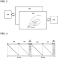
- FIG. 3 is a block diagram schematically showing the configuration of a display device having a touch sensor of an embodiment of the present disclosure
- FIG. 4 is a waveform diagram schematically illustrating a driving method of the display device having the touch sensor of an embodiment of the present application
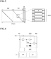
- FIG. 5 is a view illustrating a scan signal output scheme for multi-sensing of an embodiment of the present application.
- a display panel 150 displaying an image may have a touch sensor 155 capable of receiving a user's input in a touch manner.
- the touch sensor 155 may have touch electrodes for detecting presence or absence and location information of a touch on the display panel 150.
- the touch sensor 155 may operate in a capacitive manner.
- the display panel 150 may be driven by the data driver 140 connected to a data line.
- the touch sensor 155 may be driven by a touch driver 145 connected to a sensing line.
- the display panel 150 and the touch sensor 155 may be separately formed as separate components or may be integrated into one panel.
- the touch sensor 155 may be separately formed on the display panel 150 or may be implemented as an electrode formed on or inside the display panel 150.
- the touch sensor 155 is implemented as an electrode formed on the display panel 150.
- the touch sensor 155 is implemented as an electrode formed on the display panel 150
- the display panel 150 and the touch sensor 155 may be separately controlled (driven) in a time division manner.
- an image display operation of the display panel 150 may be performed for a display period DSP and a sensing operation of the touch sensor 155 may be performed for a touch sensing period TSP.
- the display period DSP is a first time period of a first frame 1Frame (e.g., a frame period).
- the touch sensing period TSP is a second time period of the first frame 1Frame. This flow may appear identically in all frames including a second frame 2Frame.
- each of the first frame 1Frame and second frame 2Frame (e.g., a frame period) includes a display period DSP during which an image is displayed during the frame period and a touch sensing period TSP during which touch is sensed during the frame period.
- the display device of the present embodiment may include a real-time sensing period RTS for determining whether an element included in the display panel 150, for example, a driving transistor or an organic light emitting diode has deteriorated and compensating for the deterioration.
- RTS real-time sensing period
- the real-time sensing period RTS may be included in a blank period VB of a frame, not in an active period including the display period DSP and the touch sensing period TSP of the frame.
- a frame e.g., the first frame 1Frame
- a circuit associated with a sensing operation may define and control a specific line as a sensing line SL and sense an element included in at least one sub-pixel included in or connected to the sensing line SL.
- the display device of an embodiment of the present application may output a multi-scan signal MSCO to drive and sense a plurality of sensing lines connected to a plurality of touch electrodes during the touch sensing period TSP to determine presence or absence of a touch.
- the multi-scan signal MSCO may be defined as scan signals which are simultaneously generated as an on-voltage H.
- the on-voltage H in FIG. 5 , it should be understood as a voltage capable of turning on a transistor included in a sub-pixel.
- the on-voltage H may be in the form of a low voltage rather than the high voltage depending on the type (for example, p-type) of the transistor.
- a part associated with the output of the multi-scan signal MSCO will be described below.
- FIG. 6 is an exemplary diagram of a sub-pixel capable of real-time sensing of an embodiment of the present disclosure
- FIG. 7 is a block diagram of a gate driver capable of outputting a multi-scan signal of this embodiment.
- the sub-pixel SP capable of real-time sensing of the present embodiment may include a switching transistor SW, a driving transistor DT, a sensing transistor ST, a capacitor CST, and an organic light emitting diode OLED.
- the driving transistor DT may have a gate electrode connected to a first electrode of the capacitor CST, a first electrode connected to a high-level voltage line EVDD, and a second electrode connected to an anode electrode of the organic light emitting diode OLED.
- the capacitor CST may have the first electrode connected to the gate electrode of the driving transistor DT, and a second electrode connected to the anode electrode of the organic light emitting diode OLED.
- the organic light emitting diode OLED may have the anode electrode connected to the second electrode of the driving transistor DT, and a cathode electrode connected to a low-level voltage line EVSS.
- the switching transistor SW may have a gate electrode connected to a first gate line GL1, a first electrode connected to a first data line DL1, and a second electrode connected to the gate electrode of the driving transistor DT.
- the sensing transistor ST may have a gate electrode connected to the first gate line GL1, a first electrode connected to a first reference line REF1, and a second electrode connected to the anode electrode of the organic light emitting diode OLED.
- the sensing transistor ST is a part of the compensation circuit which is additionally provided to compensate for deterioration (in a threshold voltage, mobility, or the like) of the driving transistor DT or organic light emitting diode OLED.
- the sensing transistor ST may enable physical sensing based on a source following operation of the driving transistor DT.
- the sensing transistor ST may operate to acquire a sensed voltage through a sensing node defined between the driving transistor DT and the organic light emitting diode OLED.
- switching transistor SW and the sensing transistor ST have been shown and described in FIG. 6 as an example as being connected in common to one first gate line GL1 and turned on or off at the same time, they may be separated from each other to be connected to different gate lines, respectively and/or may be activated separately from each other.
- the data driver 140 may include a panel driving circuit 141 configured to drive the sub-pixel SP, and a panel sensing circuit 143 configured to sense the sub-pixel SP.
- the panel driving circuit 141 may be connected to the first data line DL1.
- the panel sensing circuit 143 may be connected to the first reference line REF1.
- the panel driving circuit 141 may output a data voltage, etc. for driving of the sub-pixel SP through the first data line DL1 during the display period DSP of FIG. 4 .
- the panel sensing circuit 143 may acquire a sensing voltage for sensing of the sub-pixel SP through the first reference line REF 1 during the real-time sensing period RTS of FIG. 4 .
- the data driver 140 may transfer a sensed voltage to a timing controller, etc.
- the timing controller, etc. may create a compensation value corresponding to deterioration (a threshold voltage, mobility, or the like) of the driving transistor DT or organic light emitting diode OLED based on the sensed voltage and compensate a data signal, etc. based on the compensation value.
- the sub-pixel SP may have a touch electrode configured based on a transistor capable of separating the anode electrode or cathode electrode of the organic light emitting diode OLED.
- the touch electrode can be implemented as an anode or cathode electrode of an OLED included in a subpixel.
- a touch electrode may be configured by grouping a plurality of sub-pixels SP into one.
- various schemes of configuring a touch electrode for implementation of a touch sensor in a display panel have been proposed, and thus parts constituting the touch electrode are not shown to prevent the embodiment from being limited to a specific touch electrode structure.
- the gate driver 130 may include a control signal output unit 135 and a shift register 131.
- the gate driver 130 may be capable of outputting the multi-scan signal.
- the control signal output unit 135 may output a start signal Vst, a reset signal Rst, a selection signal Lsp, carry clock signals Cclks and scan clock signals Scclks under control of the timing controller.
- the control signal output unit 135 may be included in a level shifter or a power supply depending on how a light emitting display device is implemented.
- At least one of the signals output from the control signal output unit 135 may be directly output from the timing controller and applied to the shift register 131.
- the shift register 131 may operate based on at least one of the start signal Vst, the reset signal Rst, the selection signal Lsp, the carry clock signals Cclks and the scan clock signals Scclks output from the control signal output unit 135.
- the shift register 131 may output scan signals through gate lines GL1 to GLm.
- the shift register 131 may include a plurality of stages STG1 to STGm configured to output the scan signals corresponding to the gate lines GL1 to GLm.
- the stages STG1 to STGm may be connected in cascade such that the front and rear ones thereof are operatively associated with each other. I.e. the one stage receives a signal from the preceding stage and the next stage receives a signal output by the one stage.
- the shift register 131 may be formed on a non-active area of the display panel, preferably in a gate-in-panel (GIP) manner by a thin film process which is performed during manufacture of the display panel.
- the shift register 131 may forwardly or backwardly output the scan signals through the gate lines GL1 to GLm of the display panel, wherein forwardly means that the scan signal is output from the top to the bottom of the display panel and backwardly means that the scan signal is output from the bottom to the top of the display panel.
- the shift register 131 may select at least two of the gate lines GL1 to GLm and output the multi-scan signal to the selected gate lines, as will hereinafter be described.
- FIG. 8 is a circuit diagram showing a part of an Nth stage included in a shift register of a first embodiment of the disclosure
- FIG. 9 is a view illustrating node states when a multi-scan signal is output from the shift register shown in FIG. 8
- FIG. 10 is a view illustrating that the multi-scan signal is output from two stages included in the shift register of an embodiment
- FIG. 11 is a waveform diagram illustrating a driving scheme associated with the output of the multi-scan signal from the two stages shown in FIG. 10 of an embodiment of the application.
- the Nth stage SCG[n] of the first embodiment is a scan signal output circuit included in the shift register.
- the Nth stage SCG[n] may include a driving circuit SCP, a node controller NCP, and an output circuit SOP.
- the driving circuit SCP may initiate the operation thereof based on a start signal input through a start signal line VST, a reset signal input through a reset signal line RST, and a selection signal input through a selection signal line LSP.
- the driving circuit SCP may be driven based on a first high voltage input through a first high voltage line GVDD, a gate low voltage input through a gate low line VGL (or a third low voltage line GVSS2), and a third low voltage input through the third low voltage line GVSS2 and control the node controller NCP.
- the driving circuit SCP may include a first transistor Ta, a second transistor Tb, a third transistor Tc, a fourth transistor T1b, a fifth transistor T1c, a sixth transistor T3nb, a seventh transistor T3nc, an eighth transistor T3md, and a holding capacitor Cm in one embodiment.
- the driving circuit SCP may include an M node, Q node and a Qh node.
- the M node is connected to one electrode of the eight transistors T3md, one electrode of the second transistor Tb and a gate electrode of the third transistor Tc.
- the Q node is located and connected to one electrode of the fifth transistor T1c and one electrode of the sixth transistor T3nb.
- the Qh node is connected to the other electrode of the sixth transistor T3nb and one electrode of the seventh transistor T3nc.
- the first transistor Ta may have a gate electrode connected to an (N-i)th carry signal output terminal C[n-i] (where i is an integer which is greater than or equal to 1) and a first electrode connected to the selection signal line LSP.
- the first transistor Ta may be turned on in response to an (N-i)th carry signal output through the (N-i)th carry signal output terminal C[n-i] and transfer the selection signal input through the selection signal line LSP to a second electrode of the first transistor Ta.
- the second transistor Tb may have a gate electrode connected to the (N-i)th carry signal output terminal C[n-i], a first electrode connected to the second electrode of the first transistor Ta, and a second electrode connected to an M node Mn.
- the second transistor Tb may be turned on in response to the (N-i)th carry signal output through the (N-i)th carry signal output terminal C[n-i] and transfer the selection signal output through the second electrode of the first transistor Ta to the M node Mn.
- the third transistor Tc may have a gate electrode connected to the M node Mn, a first electrode connected to the first high voltage line GVDD, and a second electrode connected to the second electrode of the first transistor Ta and the first electrode of the second transistor Tb.
- the third transistor Tc may be turned on in response to a voltage at the M node Mn and transfer the first high voltage input through the first high voltage line GVDD to the first electrode of the second transistor Tb.
- the fourth transistor T1b may have a gate electrode connected to the M node Mn, a first electrode connected to the first high voltage line GVDD, and a second electrode connected to a first electrode of the fifth transistor T1c.
- the fourth transistor T1b may be turned on in response to the voltage at the M node Mn and transfer the first high voltage input through the first high voltage line GVDD to the first electrode of the fifth transistor T1c.
- the fifth transistor T1c may have a gate electrode connected to the reset signal line RST, the first electrode connected to the second electrode of the fourth transistor T1b, and a second electrode connected to a Q node Q.
- the fifth transistor T1c may be turned on in response to the reset signal input through the reset signal line RST and transfer the first high voltage input through the second electrode of the fourth transistor T1b to the Q node Q. That is, when the fifth transistor T1c is turned on, the Q node Q may enter a charge state.
- the sixth transistor T3nb may have a gate electrode connected to the start signal line VST, a first electrode connected to the Q node Q, and a second electrode connected to a first electrode of the seventh transistor T3nc.
- the sixth transistor T3nb may be turned on in response to the start signal input through the start signal line VST and transfer the third low voltage input through the first electrode of the seventh transistor T3nc to the Q node Q.
- the seventh transistor T3nc may have a gate electrode connected to the start signal line VST, the first electrode connected to the second electrode of the sixth transistor T3nb, and a second electrode connected to the third low voltage line GVSS2.
- the seventh transistor T3nc may be turned on in response to the start signal input through the start signal line VST and transfer the third low voltage input through the third low voltage line GVSS2 to the second electrode of the sixth transistor T3nb. That is, when the sixth transistor T3nb and the seventh transistor T3nc are turned on at the same time, the Q node Q may enter a discharge state.
- the eighth transistor T3md may have a gate electrode connected to the start signal line VST, a first electrode connected to the M node Mn, and a second electrode connected to the gate low line VGL (or the third low voltage line GVSS2).
- the eighth transistor T3md may be turned on in response to the start signal input through the start signal line VST and transfer the third low voltage input through the third low voltage line GVSS2 to the M node Mn. That is, when the eighth transistor T3md is turned on, the M node Mn may enter a discharge state (a discharge state for reset).
- the holding capacitor Cm may have a first electrode connected to the first high voltage line GVDD, and a second electrode connected to the gate electrode of the fourth transistor T1b and the gate electrode of the third transistor Tc.
- the holding capacitor Cm may store the selection signal applied to the M node Mn in the form of a voltage.
- the holding capacitor Cm may provide a voltage capable of turning on the fourth transistor T1b for a touch sensing period.
- the node controller NCP may be controlled by the driving circuit SCP to control the Q node Q, a Qh node Qh, and a Qb node Qb.
- the node controller NCP may charge or discharge at least one of the Q node Q, the Qh node Qh, or the Qb node Qb in response to a voltage transferred from the driving circuit SCP.
- the Q node Q and the Qb node Qb may be in opposite operation states. For example, when any one node is in a charge state, the other node may be in a discharge state.
- the node controller NCP may be driven based on the first high voltage input through the first high voltage line GVDD, a second high voltage input through a second high voltage line GVDD1, a second low voltage input through a second low voltage line GVSS1, and the third low voltage input through the third low voltage line GVSS2 and control the Q node Q, the Qh node Qh, and the Qb node Qb.
- the node controller NCP may be implemented based on a variety of circuits, which is shown in a box shape.
- the output circuit SOP may operate in response to the charge or discharge state of the Q node Q and Qb node Qb included in the node controller NCP and output a carry signal and a scan signal through a carry signal output terminal C[n] and a scan signal output terminal SCO[n], respectively.
- the output circuit SOP may output a carry clock signal input through a carry clock signal line CRCLK[n] as the carry signal of an on-voltage and output a scan clock signal input through a scan clock signal line SCCLK[n] as the scan signal of the on-voltage.
- the output circuit SOP may output the third low voltage input through the third low voltage line GVSS2 as the carry signal of an off-voltage and output a first low voltage input through a first low voltage line GVSS0 as the scan signal of the off-voltage.
- the output circuit SOP may include a first-1 carry output transistor T6c, a first-2 carry output transistor T7c, a first carry output capacitor CC, a first-1 scan output transistor T61, a first-2 scan output transistor T71, and a first scan output capacitor C1.
- the first carry output capacitor CC is a bootstrapping capacitor, which may have a first electrode connected to the Q node Q and a gate electrode of the first-1 carry output transistor T6c, and a second electrode connected to the carry signal output terminal C[n].
- the first carry output capacitor CC may act to raise an output level when the carry signal of the on-voltage is output.
- the first-1 carry output transistor T6c is a pull-up transistor, which may have the gate electrode connected to the Q node Q, a first electrode connected to the carry clock signal line CRCLK[n], and a second electrode connected to the carry signal output terminal C[n].
- the first-1 carry output transistor T6c may be turned on in response to a voltage at the Q node Q and output the carry clock signal as the carry signal of the on-voltage.
- the first-2 carry output transistor T7c is a pull-down transistor, which may have a gate electrode connected to the Qb node Qb, a first electrode connected to the carry signal output terminal C[n], and a second electrode connected to the third low voltage line GVSS2.
- the first-2 carry output transistor T7c may be turned on in response to a voltage at the Qb node Qb and output the third low voltage as the carry signal of the off-voltage.
- the first scan output capacitor C1 is a bootstrapping capacitor, which may have a first electrode connected to the Q node Q and a gate electrode of the first-1 scan output transistor T61, and a second electrode connected to the scan signal output terminal SCO[n].
- the first scan output capacitor C1 may act to raise an output level when the scan signal of the on-voltage is output.
- the first-1 scan output transistor T61 is a pull-up transistor, which may have the gate electrode connected to the Q node Q, a first electrode connected to the scan clock signal line SCCLK[n], and a second electrode connected to the scan signal output terminal SCO[n].
- the first-1 scan output transistor T61 may be turned on in response to the voltage at the Q node Q and output the scan clock signal as the scan signal of the on-voltage.
- the first-2 scan output transistor T71 is a pull-down transistor, which may have a gate electrode connected to the Qb node Qb, a first electrode connected to the scan signal output terminal SCO[n], and a second electrode connected to the first low voltage line GVSS0.
- the first-2 scan output transistor T71 may be turned on in response to the voltage at the Qb node Qb and output the first low voltage as the scan signal of the off-voltage.
- the first high voltage and the second high voltage may have the same voltage level or may have a slight level difference therebetween.
- the first low voltage, the second low voltage and the third low voltage may have the same voltage level or may have a slight level difference there among. Nevertheless, the reason for dividing the voltage lines is that the voltage levels may be the same or different depending on the purpose and effect.
- the Nth stage SCG[n] of the first embodiment may output a multi-scan signal when the M node Mn and the Q node Q are charged for the touch sensing period TSP of FIG. 4 .
- the multi-scan signal are scan signals simultaneously output from a plurality of stages, not one stage of one embodiment.
- the Nth stage SCG[n] and an (N+1)th stage SCG[n+1] may be configured based on the same circuit, but may have a difference in connection relationship of signal lines as will be described below.
- the gate electrodes of the first transistor Ta and second transistor Tb may be connected to a carry signal output terminal C[n-1] of an (N-1)th stage, which is a previous stage.
- the first electrode of the first-1 carry output transistor T6c may be connected to the Nth carry clock signal line CRCLK[n]
- the first electrode of the first-1 scan output transistor T61 may be connected to the Nth scan clock signal line SCCLK[n].
- the gate electrodes of the first transistor Ta and second transistor Tb may be connected to the carry signal output terminal C[n] of the Nth stage, which is a previous stage.
- the first electrode of the first-1 carry output transistor T6c may be connected to an (N+1)th carry clock signal line CRCLK[n+1]
- the first electrode of the first-1 scan output transistor T61 may be connected to an (N+1)th scan clock signal line SCCLK[n+1].
- the Nth stage SCG[n] and the (N+1)th stage SCG[n+1] may be reset in response to a reset signal Rst of the on-voltage H applied for an initial driving period IDRV. Then, the Nth stage SCG[n] and the (N+1)th stage SCG[n+1] may initiate driving thereof in response to a start signal Vst and a selection signal Lsp of the on-voltage H applied for the initial driving period IDRV.
- the Nth stage SCG[n] and the (N+1)th stage SCG[n+1] may output carry signals and scan signals in response to selection signals Lsp, carry clock signals Cclk1 to Cclk3 and scan clock signals Scclk1 to Scclk8 of the on-voltage H applied for a display period DSP.
- the Nth stage SCG[n] and the (N+1)th stage SCG[n+1] may be reset in response to the reset signal Rst, and the M nodes Mn and Q nodes Q thereof may be charged by the selection signals Lsp applied during the display period DSP.
- a plurality of stages may be driven to output a multi-scan signal MSCO.
- the total number of drivable stages may correspond to the total number of times the selection signals Lsp are output during the display period DSP.
- the number of stages which can be driven simultaneously to output scan signals that collectively form the multi-scan signal MSCO may be two.
- a touch sensor formed on a display panel may perform a touch sensing operation for sensing presence or absence of a touch at a plurality of locations in response to the multi-scan signal MSCO output from the Nth stage SCG[n] and (N+1)th stage SCG[n+1].
- a first location and a second location may be sensed for touch during the touch sensing period TSP in response to the scan signals output by the Nth stage SCG[n] and (N+1)th stage SCG[n+1] that collectively form the multi-scan signal MSCO.
- FIG. 12 is a circuit diagram showing a part of an Nth stage included in a shift register of a second embodiment of the present disclosure
- FIG. 13 is an exemplary diagram of the circuit configuration of a node controller shown in FIG. 12 of the second embodiment of the present disclosure
- FIG. 14 is a view illustrating node states when a multi-scan signal is output from the shift register shown in FIG. 12 of the second embodiment of the present disclosure
- FIG. 15 is a view illustrating that the multi-scan signal is output from two stages included in the shift register of the second embodiment of the present disclosure
- FIG. 16 is a waveform diagram illustrating a driving scheme associated with the output of the multi-scan signal from the two stages shown in FIG. 15 of the second embodiment of the present disclosure.
- the Nth stage SCG[n] of the second embodiment is a scan signal output circuit included in the shift register.
- the Nth stage SCG[n] may include a driving circuit SCP, a node controller NCP, and an output circuit SOP.
- the Nth stage SCG[n] of the second embodiment has a difference in configuration of the node controller NCP and output circuit SOP compared to the first embodiment, which will hereinafter be described.
- the output circuit SOP of the Nth stage SCG[n] of the second embodiment may further include a first-1 scan output transistor T61, a first-2 scan output transistor T71, a first scan output capacitor C1, a second-1 scan output transistor T62, a second-2 scan output transistor T72, a second scan output capacitor C2, a third-1 scan output transistor T63, a third-2 scan output transistor T73, a third scan output capacitor C3, a fourth-1 scan output transistor T64, a fourth-2 scan output transistor T74, and a fourth scan output capacitor C4.
- the first-1 scan output transistor T61, the first-2 scan output transistor T71 and the first scan output capacitor C1 may output an Nth scan signal (first scan signal) through an Nth scan signal output terminal SCO[n].
- the second-1 scan output transistor T62, the second-2 scan output transistor T72 and the second scan output capacitor C2 may output an (N+1)th scan signal (second scan signal) through an (N+1)th scan signal output terminal SCO[n+1].
- the third-1 scan output transistor T63, the third-2 scan output transistor T73 and the third scan output capacitor C3 may output an (N+2)th scan signal (third scan signal) through an (N+2)th scan signal output terminal SCO[n+2].
- the fourth-1 scan output transistor T64, the fourth-2 scan output transistor T74 and the fourth scan output capacitor C4 may output an (N+3)th scan signal (fourth scan signal) through an (N+3)th scan signal output terminal SCO[n+3].
- the node controller NCP of the Nth stage SCG[n] of the second embodiment may include a first node control transistor T1, a second node control transistor T1a, a third node control transistor T3q, a fourth node control transistor T3q', a fifth node control transistor T3n, a sixth node control transistor T3na, a seventh node control transistor T3, an eighth node control transistor T3a, a ninth node control transistor T4, a tenth node control transistor T41, an eleventh node control transistor T41', a twelfth node control transistor T4q, a thirteenth node control transistor T5q, a fourteenth node control transistor T5, a fifteenth node control transistor T5s, a sixteenth node control transistor T5n, a seventeenth node control transistor T5h, an eighteenth node control transistor T5a, and a nineteenth node control transistor T5b.
- the first node control transistor T1 and the second node control transistor T1a may be turned on in response to an (N-i)th carry signal output through an (N-i)th carry signal output terminal C[n-i] (where i is an integer which is greater than or equal to 1) and control a Q node Q based on a forward signal input through a forward terminal FW.
- the third node control transistor T3q and the fourth node control transistor T3q' may be turned on in response to a voltage at the Q node Q and control a Qh node Qh based on a first high voltage input through a first high voltage line GVDD.
- the fifth node control transistor T3n and the sixth node control transistor T3na may be turned on in response to an (N+i)th carry signal output through an (N+i)th carry signal output terminal C[n+i] (where i is an integer which is greater than or equal to 1) and control the Q node Q and the Qh node Qh based on a backward signal input through a backward terminal BW.
- the seventh node control transistor T3 and the eighth node control transistor T3a may be turned on in response to a voltage at a Qb node Qb and control the Q node Q and the Qh node Qh based on a third low voltage input through a third low voltage line GVSS2.
- the eleventh node control transistor T41' and the tenth node control transistor T41 may be turned on in response to a second high voltage line GVDD1.
- the twelfth node control transistor T4q may be turned on in response to the voltage at the Q node Q.
- the ninth node control transistor T4 may be turned on in response to a node voltage between the eleventh node control transistor T41' and the twelfth node control transistor T4q to control the thirteenth node control transistor T5q based on a second high voltage input through a second high voltage line GVDD1.
- the Qb node Qb may be discharged based on the third low voltage input through the third low voltage line GVSS2.
- the fourteenth node control transistor T5 may be turned on in response to the forward signal transferred from the fifteenth node control transistor T5s or the backward signal transferred from the sixteenth node control transistor T5n and discharge the Qb node Qb based on the third low voltage input through the third low voltage line GVSS2.
- the fifteenth node control transistor T5s may be turned on in response to the (N-i)th carry signal transferred from the (N-i)th carry signal output terminal C[n-i] (where i is an integer which is greater than or equal to 1) and transfer the forward signal input through the forward terminal FW to a gate electrode of the fourteenth node control transistor T5 and a first electrode of the seventeenth node control transistor T5h.
- the sixteenth node control transistor T5n may be turned on in response to the (N+i)th carry signal transferred from the (N+i)th carry signal output terminal C[n+i] (where i is an integer which is greater than or equal to 1) and transfer the backward signal input through the backward terminal BW to the gate electrode of the fourteenth node control transistor T5 and the first electrode of the seventeenth node control transistor T5h.
- the seventeenth node control transistor T5h may be turned on in response to the voltage at the Qb node Qb and discharge the Qb node Qb based on the third low voltage input through the third low voltage line GVSS2.
- the eighteenth node control transistor T5a may be turned on in response to a reset signal input through a reset signal line RST and discharge the Qb node Qb based on the third low voltage transferred from the nineteenth node control transistor T5b.
- the nineteenth node control transistor T5b may be turned on based on a voltage at an M node Mn and transfer the third low voltage input through the third low voltage line GVSS2 to a second electrode of the eighteenth node control transistor T5a.
- the Nth stage SCG[n] of the second embodiment may output a multi-scan signal when the M node Mn and the Q node Q are charged for the touch sensing period TSP of FIG. 4 .
- the multi-scan signal may mean scan signals output from a plurality of stages, not one stage.
- the Nth stage SCG[n] and an (N+1)th stage SCG[n+1] may be configured based on the same circuit, but may have a difference in connection relationship of signal lines as will be described below.
- the gate electrodes of the first transistor Ta and second transistor Tb may be connected to a carry signal output terminal C[n-1] of an (N-1)th stage, which is a previous stage.
- the first electrode of the first-1 carry output transistor T6c may be connected to the Nth carry clock signal line CRCLK[n].
- a first electrode of the first-1 scan output transistor T61 may be connected to an Nth scan clock signal line SCCLK[n]
- a first electrode of the second-1 scan output transistor T62 may be connected to an (N+1)th scan clock signal line SCCLK[n+1]
- a first electrode of the third-1 scan output transistor T63 may be connected to an (N+2)th scan clock signal line SCCLK[n+2]
- a first electrode of the fourth-1 scan output transistor T64 may be connected to an (N+3)th scan clock signal line SCCLK[n+3].
- the gate electrodes of the first transistor Ta and second transistor Tb may be connected to the carry signal output terminal C[n] of the Nth stage, which is a previous stage.
- the first electrode of the first-1 carry output transistor T6c may be connected to an (N+1)th carry clock signal line CRCLK[n+1].
- the first electrode of the first-1 scan output transistor T61 may be connected to an (N+4)th scan clock signal line SCCLK[n+4]
- the first electrode of the second-1 scan output transistor T62 may be connected to an (N+5)th scan clock signal line SCCLK[n+5]
- the first electrode of the third-1 scan output transistor T63 may be connected to an (N+6)th scan clock signal line SCCLK[n+6]
- the first electrode of the fourth-1 scan output transistor T64 may be connected to an (N+7)th scan clock signal line SCCLK[n+7].
- the Nth stage SCG[n] and the (N+1)th stage SCG[n+1] may be reset in response to a reset signal Rst of the on-voltage H applied for an initial driving period IDRV. Then, the Nth stage SCG[n] and the (N+1)th stage SCG[n+1] may initiate driving thereof in response to a start signal Vst and a selection signal Lsp of the on-voltage H applied for the initial driving period IDRV.
- the Nth stage SCG[n] and the (N+1)th stage SCG[n+1] may output carry signals and scan signals in response to selection signals Lsp, carry clock signals Cclk1 to Cclk3 and scan clock signals Scclk1 to Scclk8 of the on-voltage H applied for a display period DSP.
- the Nth stage SCG[n] and the (N+1)th stage SCG[n+1] may be reset in response to the reset signal Rst, and the M nodes Mn and Q nodes Q thereof may be charged by the selection signals Lsp applied during the display period DSP.
- a plurality of stages may be driven to output a multi-scan signal MSCO.
- the total number of drivable stages may correspond to the total number of times the selection signals Lsp are output during the display period DSP.
- the number of stages which can be driven simultaneously to output scan signal that collectively form the multi-scan signal MSCO may be four.
- a touch sensor formed on a display panel may perform a touch sensing operation for sensing presence or absence of a touch at a plurality of locations in response to the multi-scan signal MSCO output from the Nth stage SCG[n] and (N+1)th stage SCG[n+1].
- a plurality of stages are selectively driven and a touch sensing operation is performed at a plurality of locations based on a multi-scan signal output from the selectively driven stages, thereby making it possible to reduce time required for touch sensing.
- embodiments of the present disclosure provide a gate driving circuit capable of selectively driving a plurality of stages based on a selection signal, and a display device capable of image display, touch sensing, and real-time sensing based on the gate driving circuit.
Landscapes
- Engineering & Computer Science (AREA)
- Theoretical Computer Science (AREA)
- Physics & Mathematics (AREA)
- General Physics & Mathematics (AREA)
- General Engineering & Computer Science (AREA)
- Computer Hardware Design (AREA)
- Human Computer Interaction (AREA)
- Quality & Reliability (AREA)
- Chemical & Material Sciences (AREA)
- Crystallography & Structural Chemistry (AREA)
- Control Of Indicators Other Than Cathode Ray Tubes (AREA)
- Shift Register Type Memory (AREA)
- Control Of El Displays (AREA)
Abstract

Description
- This application claims the priority of Republic of
Korea Patent Application No. 10-2023-0011717, filed on January 30, 2023 - The present disclosure relates to a gate driving circuit and a display device including the same.
- With the development of the information technology, the market for display devices that are media for connection between users and information is growing. Accordingly, display devices such as a light emitting display (LED), a quantum dot display (QDD), and a liquid crystal display (LCD) have been increasingly used.
- The above display devices each include a display panel including sub-pixels, a driver which outputs a driving signal for driving of the display panel, and a power supply which generates power to be supplied to the display panel or the driver.
- In such a display device, when sub-pixels formed in a display panel are supplied with driving signals, for example, a scan signal and a data signal, a selected one of the sub-pixels may transmit light therethrough or directly emit light, thereby displaying an image.
- Accordingly, the present disclosure is directed to a gate driving circuit and a display device including the same that substantially obviate one or more problems due to limitations and disadvantages of the related art.
- Embodiments of the present disclosure provide a gate driving circuit and a display device including the same in which a plurality of stages of the gate driver are selectively driven and a touch sensing operation is performed at a plurality of locations based on a multi-scan signal output from the selectively selected driven stages, thereby making it possible to reduce time required for touch sensing.
- Additional advantages, objects, and features of the disclosure will be set forth in part in the description which follows and in part will become apparent to those having ordinary skill in the art upon examination of the following or may be learned from practice of the disclosure. The objectives and other advantages of the disclosure may be realized and attained by the structure particularly pointed out in the written description and claims hereof as well as the appended drawings.
- The object is solved by the features of the independent claims. Preferred embodiments are given in the dependent claims.
- In one embodiment, a gate driving circuit comprises: a driving circuit configured to charge an M node with a selection signal externally supplied to the driving circuit responsive to the driving circuit receiving a first carry signal, and charge a Q node with a high voltage responsive to a reset signal and a voltage charged in the M node that corresponds to the selection signal; a node controller connected to the driving circuit, the node controller configured to control the Q node and a Qb node responsive to driving of the driving circuit, wherein a level of a voltage at the Qb node is opposite to a level of a voltage at the Q node; and an output circuit connected to the node controller, the output circuit configured to output a second carry signal and at least one scan signal responsive to the voltage at the Q node and the voltage at the Qb node included in the node controller.
- In one embodiment, a display device comprises: a display panel comprising a sub-pixel configured to display a portion of an image, and a touch electrode configured to sense a touch of the display panel; and a gate driving circuit comprising a plurality of stages configured to supply scan signals to the display panel, wherein a stage among the plurality of stages comprises: a driving circuit configured to charge an M node based on a selection signal externally supplied to the driving circuit responsive to receiving a carry signal received from another stage from the plurality of stages and charge a Q node with a high voltage responsive to a reset signal and a voltage charged in the M node that corresponds to the selection signal, a node controller connected to the driving circuit, the node controller configured to control the Q node and a Qb node responsive to driving of the driving circuit, wherein a level of a voltage at the Qb node is opposite to a level of a voltage at the Q node, and an output circuit connected to the node controller, the output circuit configured to output a carry signal and at least one scan signal responsive to the voltage at the Q node and the voltage at the Qb node included in the node controller, wherein at least two stages among the plurality of stages simultaneously output scan signals responsive to the selection signal during a touch sensing period during which touch of the touch electrode is sensed, the outputted scan signals generated as an on-voltage during the touch sensing period.
- In one embodiment, a display device comprises: a display panel comprising a plurality of touch electrodes and a plurality of subpixels including a first subpixel and a second subpixel, the plurality of touch electrodes configured to sense a touch of the display panel during a touch sensing period of a frame period, and the plurality of subpixels configured to display an image during a display driving period of the frame period; and a gate driving circuit comprising a plurality of stages configured to output a plurality of scan signals to the plurality of subpixels, the plurality of stages including a first stage connected to the first subpixel and a second stage connected to the second subpixel, wherein during the touch sensing period the first stage is configured to output a first scan signal from the plurality of scan signals to the first subpixel to sense touch of a first location of the display panel and the second stage is configured to output a second scan signal to the second subpixel at a same time that the first stage outputs the first scan signal to the first subpixel to sense touch of a second location of the display panel.
- In one or more embodiments, the driving circuit may comprise a first transistor, a second transistor, and a third transistor configured to charge the M node with the voltage corresponding to the selection signal responsive to the received first carry signal.
- In one or more embodiments, the driving circuit may comprise a holding capacitor configured to store the selection signal as a voltage.
- In one or more embodiments, the first transistor may comprise a gate electrode connected to a carry signal output terminal of another gate driving circuit that outputs the first carry signal received by the driving circuit, a first electrode of the first transistor connected to a selection signal line that supplies the selection signal, and a second electrode of the first transistor.
- In one or more embodiments, the second transistor may comprise a gate electrode that is connected to the carry signal output terminal of the other gate driving circuit that outputs the first carry signal received by the driving circuit, a first electrode of the second transistor that is connected to the second electrode of the first transistor, and a second electrode of the second transistor that is connected to the M node.
- In one or more embodiments, the third transistor may comprise a gate electrode of the third transistor that is connected to the second electrode of the second transistor at the M node, a first electrode of the third transistor that is connected to a high voltage line that supplies the high voltage, and a second electrode of the third transistor that is connected to the second electrode of the first transistor and the first electrode of the second transistor.
- In one or more embodiments, the holding capacitor may comprise a first electrode and a second electrode, the first electrode of the holding capacitor may be connected to the high voltage line and the first electrode of the third transistor, and the second electrode of the holding capacitor may be connected to the gate electrode of the third transistor and the second electrode of the second transistor at the M node.
- In one or more embodiments, the driving circuit may comprise a fourth transistor comprising a gate electrode of the fourth transistor that is connected to the second electrode of the holding capacitor, the gate electrode of the third transistor, and the second electrode of the second transistor at the M node, a first electrode of the fourth transistor that is connected to the high voltage line, the first electrode of the holding capacitor, and the first electrode of the third transistor, and a second electrode of the fourth transistor.
- In one or more embodiments, a fifth transistor having a gate electrode connected to a reset signal line that supplies the reset signal, a first electrode of the fifth transistor that is connected to the second electrode of the fourth transistor, and a second electrode of the fifth transistor that is connected to the Q node.
- In one or more embodiments, the driving circuit may comprise a sixth transistor comprising a gate electrode of the sixth transistor that is connected to a start signal line that supplies a start signal, a first electrode of the sixth transistor that is connected to the second electrode of the second transistor, the gate electrode of the third transistor, the second electrode of the holding capacitor, and the gate electrode of fourth transistor at the M node, and a second electrode connected to a low voltage line that supplies a low voltage that is less than the high voltage, the sixth transistor configured to discharge the M node responsive to the start signal.
- In one or more embodiments, the output circuit may comprise scan signal output terminals configured to simultaneously output scan signals generated as an on-voltage responsive to the voltage at the Q node.
- In one or more embodiments, the first stage may comprise a first driving circuit, a first node controller and a first output circuit.
- In one or more embodiments, the first driving circuit may be configured to charge a M node of the first driving circuit based on a selection signal externally supplied to the first driving circuit responsive to receiving a carry signal from another stage from the plurality of stages.
- In one or more embodiments, the first driving circuit may be configured to charge a Q node of the first stage with a high voltage responsive to a reset signal and a voltage charged in the M node of the first driving circuit that corresponds to the selection signal.
- In one or more embodiments, the first node controller may be connected to the first driving circuit.
- In one or more embodiments, the first node controller may be configured to control the Q node and a Qb node of the first node controller responsive to driving of the first driving circuit.
- In one or more embodiments, a level of a voltage of the Qb node of the first node controller may be opposite to a level of a voltage of the Q node of the first node controller.
- In one or more embodiments, a first output circuit may be connected to the first node controller.
- In one or more embodiments, the first output circuit may be configured to output the first scan signal to the first subpixel and a first carry signal and responsive to the voltage at the Q node and the voltage at the Qb node included in the first node controller.
- In one or more embodiments, the second stage may comprise a second driving circuit, a second node controller and a second output circuit.
- In one or more embodiments, the second driving circuit may be configured to charge a M node of the second driving circuit based on the selection signal externally supplied to the second driving circuit responsive to the first carry signal received from the first stage.
- In one or more embodiments, the second driving circuit may be configured to charge a Q node of the second stage with the high voltage responsive to the reset signal and a voltage charged in the M node of the second driving circuit that corresponds to the selection signal.
- In one or more embodiments, the second node controller may be connected to the second driving circuit.
- In one or more embodiments, the second node controller may be configured to control the Q node and a Qb node of the second node controller responsive to driving of the second driving circuit.
- In one or more embodiments, a level of a voltage of the Qb node of the second node controller may be opposite to a level of a voltage of the Q node of the second node controller.
- In one or more embodiments, the second output circuit may be connected to the second node controller.
- In one or more embodiments, the second output circuit may be configured to output the second scan signal to the second subpixel and a second carry signal responsive to the voltage at the Q node and the voltage at the Qb node included in the second node controller.
- In one or more embodiments, the first output circuit may output the first scan signal to the first subpixel at a same time that the second output circuit outputs the second scan signal to the second subpixel.
- In one or more embodiments, the first output circuit may be configured to output a first plurality of scan signals that include the first scan signal during the touch sensing period.
- In one or more embodiments, the second output circuit may be configured to output a second plurality of scan signals that include the second scan signal during the touch sensing period at a same time that the first output circuit outputs the first plurality of scan signals.
- In one or more embodiments, each of the first plurality of scan signals and each of the second plurality of scan signals may be applied to a corresponding one subpixel from the plurality of subpixels to sense touch of the display panel.
- In one or more embodiments, the first driving circuit may comprise a first transistor of the first driving circuit including a gate electrode of the first transistor that is connected to a carry signal output terminal of the other stage that outputs the carry signal received by the first driving circuit, a first electrode of the first transistor that is connected to a selection signal line that supplies the selection signal, and a second electrode of the first transistor.
- In one or more embodiments, the first driving circuit may comprise a second transistor of the first driving circuit including a gate electrode of the second transistor that is connected to the carry signal output terminal of the other stage that outputs the carry signal received by the first driving circuit, a first electrode of the second transistor that is connected to the second electrode of the first transistor of the first driving circuit, and a second electrode of the second transistor that is connected to the M node of the first driving circuit.
- In one or more embodiments, the first driving circuit may comprise a third transistor of the first driving circuit including a gate electrode of the third transistor that is connected to the second electrode of the second transistor at the M node of the first driving circuit, a first electrode of the third transistor that is connected to a voltage line that supplies the high voltage, and a second electrode of the third transistor that is connected to the second electrode of the first transistor and the first electrode of the second transistor.
- In one or more embodiments, the first driving circuit may comprise a first holding capacitor of the first driving circuit including a first electrode and a second electrode, the first electrode of the first holding capacitor connected to the high voltage line and the first electrode of the third transistor, and the second electrode of the first holding capacitor connected to the gate electrode of the third transistor and the second electrode of the second transistor at the M node of the first driving circuit,
- In one or more embodiments, the second driving circuit may comprise a first transistor of the second driving circuit including a gate electrode of the first transistor of the second driving circuit that is connected to a carry signal output terminal of the first stage that outputs the first carry signal received by the second driving circuit, a first electrode of the first transistor of the second driving circuit that is connected to the selection signal line that supplies the selection signal, and a second electrode of the first transistor of the second driving circuit.
- In one or more embodiments, the second driving circuit may comprise a second transistor of the second driving circuit including a gate electrode of the second transistor of the second driving circuit that is connected to the carry signal output terminal of the first stage that outputs the carry signal received by the second driving circuit, a first electrode of the second transistor of the second driving circuit that is connected to the second electrode of the first transistor of the second driving circuit, and a second electrode of the second transistor that is connected to the M node of the second driving circuit.
- In one or more embodiments, the second driving circuit may a third transistor of the second driving circuit including a gate electrode of the third transistor of the second driving circuit that is connected to the second electrode of the second transistor of the second driving circuit at the M node of the second driving circuit, a first electrode of the third transistor of the second driving circuit that is connected to the voltage line that supplies the high voltage, and a second electrode of the third transistor of the second driving circuit that is connected to the second electrode of the first transistor of the second driving circuit and the first electrode of the second transistor of the second driving circuit.
- In one or more embodiments, the second driving circuit may a second holding capacitor of the second driving circuit including a first electrode and a second electrode, the first electrode of the second holding capacitor may be connected to the high voltage line and the first electrode of the third transistor of the second driving circuit, and the second electrode of the second holding capacitor may be connected to the gate electrode of the third transistor of the second driving circuit and the second electrode of the second transistor of the second driving circuit at the M node of the second driving circuit.
- In one or more embodiments, the first driving circuit may comprise a fourth transistor of the first driving circuit comprising a gate electrode of the fourth transistor that is connected to the second electrode of the first holding capacitor, the gate electrode of the third transistor of the first driving circuit, and the second electrode of the second transistor of the first driving circuit at the M node of the first driving circuit, a first electrode of the fourth transistor that is connected to the high voltage line, the first electrode of the first holding capacitor, and the first electrode of the third transistor of the first driving circuit, and a second electrode of the fourth transistor of the first driving circuit.
- In one or more embodiments, the first driving circuit may comprise a fifth transistor of the first driving circuit having a gate electrode connected to a reset signal line that supplies the reset signal, a first electrode of the fifth transistor that is connected to the second electrode of the fourth transistor of the first driving circuit, and a second electrode of the fifth transistor that is connected to the Q node of the first driving circuit.
- In one or more embodiments, the second driving circuit may comprise a fourth transistor of the second driving circuit comprising a gate electrode of the fourth transistor that is connected to the second electrode of the second holding capacitor, the gate electrode of the third transistor of the second driving circuit, and the second electrode of the second transistor of the second driving circuit at the M node of the second driving circuit, a first electrode of the fourth transistor that is connected to the high voltage line, the first electrode of the second holding capacitor, and the first electrode of the third transistor of the second driving circuit, and a second electrode of the fourth transistor of the second driving circuit.
- In one or more embodiments, the second driving circuit may comprise a fifth transistor of the second driving circuit having a gate electrode connected to the reset signal line that supplies the reset signal, a first electrode of the fifth transistor that is connected to the second electrode of the fourth transistor of the second driving circuit, and a second electrode of the fifth transistor that is connected to the Q node of the second driving circuit.
- In one or more embodiments, the first driving circuit may comprises a sixth transistor of the first driving circuit comprising a gate electrode of the sixth transistor that is connected to a start signal line that supplies a start signal, a first electrode of the sixth transistor that is connected to the second electrode of the second transistor of the first driving circuit, the gate electrode of the third transistor of the first driving circuit, the second electrode of the first holding capacitor, and the gate electrode of fourth transistor of the first driving circuit at the M node of the first driving circuit, and a second electrode connected to a low voltage line that supplies a low voltage that is less than the high voltage, and the sixth transistor configured to discharge the M node of the first driving circuit responsive to the start signal.
- In one or more embodiments, the second driving circuit may comprises a sixth transistor of the second driving circuit comprising a gate electrode of the sixth transistor that is connected to the start signal line that supplies the start signal, a first electrode of the sixth transistor that is connected to the second electrode of the second transistor of the second driving circuit, the gate electrode of the third transistor of the second driving circuit, the second electrode of the second holding capacitor, and the gate electrode of fourth transistor of the second driving circuit at the M node of the second driving circuit, and a second electrode connected to the low voltage line that supplies the low voltage, and the sixth transistor configured to discharge the M node of the second driving circuit responsive to the start signal.
- In one or more embodiments, during the display driving period the selection signal may be supplied a number of times and a total number of stages from the plurality of stages that simultaneously output scan signals during the touch display period may be based on the number of times the selection signal is supplied during the display driving period.
- It is to be understood that both the foregoing general description and the following detailed description of the present disclosure are exemplary and explanatory and are intended to provide further explanation of the disclosure as claimed.
- The accompanying drawings, which are included to provide a further understanding of the disclosure and are incorporated in and constitute a part of this application, illustrate embodiment(s) of the disclosure and together with the description serve to explain the principle of the disclosure. In the drawings:
-
FIG. 1 is a block diagram schematically showing the configuration of a light emitting display device of an embodiment of the present disclosure; -
FIG. 2 schematic block diagram of a sub-pixel shown inFIG. 1 of an embodiment of the present disclosure; -
FIG. 3 is a block diagram schematically showing the configuration of a display device having a touch sensor of an embodiment of the present disclosure; -
FIG. 4 is a waveform diagram schematically illustrating a driving method of the display device having the touch sensor of an embodiment of the present disclosure ; -
FIG. 5 a view illustrating a scan signal output scheme for multi-sensing of an embodiment of the disclosure; -
FIG. 6 is an exemplary diagram of a sub-pixel capable of real-time sensing of an embodiment of the present disclosure; -
FIG. 7 is a block diagram of a gate driver capable of outputting a multi-scan signal of an embodiment of the present disclosure; -
FIG. 8 is a circuit diagram showing a part of an Nth stage included in a shift register of a first embodiment of the present disclosure; -
FIG. 9 is a view illustrating node states when a multi-scan signal is output from the shift register shown in -
FIG. 8 of an embodiment of the present disclosure; -
FIG. 10 is a view illustrating that the multi-scan signal is output from two stages included in the shift register of an embodiment of the present disclosure; -
FIG. 11 is a waveform diagram illustrating a driving scheme associated with the output of the multi-scan signal from the two stages shown inFIG. 10 of an embodiment of the present disclosure; -
FIG. 12 is a circuit diagram showing a part of an Nth stage included in a shift register of a second embodiment of the present disclosure; -
FIG. 13 is an exemplary diagram of the circuit configuration of a node controller shown inFIG. 12 of an embodiment of the present disclosure; -
FIG. 14 is a view illustrating node states when a multi-scan signal is output from the shift register shown inFIG. 12 of an embodiment of the present disclosure; and -
FIG. 15 is a view illustrating that the multi-scan signal is output from two stages included in the shift register of an embodiment of the present disclosure; and -
FIG. 16 is a waveform diagram illustrating a driving scheme associated with the output of the multi-scan signal from the two stages shown inFIG. 15 of an embodiment of the present disclosure. - A display device of the present disclosure may be implemented as a television, a video player, a personal computer (PC), a home theater, an automotive electric device, or a smartphone, but is not limited thereto. The display device of the present disclosure may be implemented by a light emitting display (LED), a quantum dot display (QDD), or a liquid crystal display (LCD). For convenience of description, an LED device that directly emits light based on an inorganic light emitting diode or an organic light emitting diode will hereinafter be taken as an example of the display device of the present disclosure.
- Thin film transistors to be described below may be implemented as n-type thin film transistors, p-type thin film transistors, or a combination of n-type and p-type thin film transistors. A thin film transistor is a three-electrode element including a gate, a source and a drain. The source is an electrode that supplies carriers to the transistor. In the thin film transistor, carriers start to flow from the source. The drain is an electrode through which carriers externally flow in the thin film transistor. Namely, carriers flow from the source to the drain in the thin film transistor.
- In the case of a p-type thin film transistor, carriers are holes and thus a source voltage is higher than a drain voltage such that the holes flow from the source to the drain. Since holes flow from the source to the drain in the p-type thin film transistor, current flows from the source to the drain. In contrast, in the case of an n-type thin film transistor, carriers are electrons and thus a source voltage is lower than a drain voltage such that the electrons flow from the source to the drain. Since electrons flow from the source to the drain in the n-type thin film transistor, current flows from the drain to the source. However, the source and the drain of a thin film transistor may be interchanged according to voltages applied thereto. In connection therewith, in the following description, any one of the source and drain will be described as a first electrode, and the other one will be described as a second electrode.
-
FIG. 1 is a block diagram schematically showing the configuration of an LED device andFIG. 2 is a schematic block diagram of a sub-pixel shown inFIG. 1 of an embodiment of the disclosure. - As shown in
FIGs. 1 and 2 , the LED device may include an image supply means 110, atiming controller 120, a gate driver (gate driving circuit) 130, a data driver (data driving circuit) 140, adisplay panel 150, and apower supply 180. - The image supply means (set or host system) 110 may output various driving signals together with an image data signal externally supplied or an image data signal stored in an internal memory. The image supply means 110 may supply the data signal and the various driving signals to the
timing controller 120. - The
timing controller 120 may output a gate timing control signal GDC for control of operation timing of thegate driver 130, a data timing control signal DDC for control of operation timing of thedata driver 140, and various synchronization signals (a vertical synchronization signal VSYNC and a horizontal synchronization signal HSYNC). Thetiming controller 120 may supply a data signal DATA supplied from theimage supply 110 together with the data timing control signal DDC to thedata driver 140. Thetiming controller 120 may be formed in the form of an integrated circuit (IC) and mounted on a printed circuit board, but is not limited thereto. - The
gate driver 130 may output a scan signal (or gate signal) in response to the gate timing control signal GDC supplied from thetiming controller 120. Thegate driver 130 may supply the scan signal to sub-pixels included in thedisplay panel 150 through gate lines GL1 to GLm. Thegate driver 130 may be formed in form of an IC or may be formed directly on thedisplay panel 150 in a gate-in-panel (GIP) manner, but is not limited thereto. - The
data driver 140 may sample and latch the data signal DATA in response to the data timing control signal DDC supplied from thetiming controller 120, convert the resulting digital data signal into an analog data voltage based on a gamma reference voltage, and output the converted analog data voltage. Thedata driver 140 may supply the data voltage to the sub-pixels included in thedisplay panel 150 through data lines DL1 to DLn. Thedata driver 140 may be formed in the form of an IC and mounted on thedisplay panel 150 or mounted on the printed circuit board, but is not limited thereto. - The
power supply 180 may generate a high-level voltage and a low-level voltage that is less than the high-level voltage based on an external input voltage externally supplied and output the generated high-level voltage and low-level voltage through a high-level voltage line EVDD and a low-level voltage line EVSS, respectively. Thepower supply 180 may generate and output a voltage required to drive thegate driver 130 or a voltage required to drive thedata driver 140, as well as the high-level voltage and the low-level voltage. - The
display panel 150 may display an image in response to a driving signal including the scan signal and the data voltage, and a driving voltage including the high-level voltage and the low-level voltage. The sub-pixels of thedisplay panel 150 directly emit light. Thedisplay panel 150 may be manufactured based on a rigid or flexible substrate of glass, silicon, polyimide, or the like. The sub-pixels which emit light may include pixels including red, green and blue or pixels including red, green, blue and white. - For example, one sub-pixel SP may be connected to the first data line DL1, the first gate line GL1, the high-level voltage line EVDD, and the low-level voltage line EVSS, and may include a pixel circuit which is composed of a switching transistor, a driving transistor, a capacitor, an organic light emitting diode, etc. The sub-pixel SP used in the LED device is complex in circuit configuration in that it directly emits light. Furthermore, there are various compensation circuits for compensating for deterioration of not only the organic light emitting diode, which emits light, but also the driving transistor, which supplies driving current required to drive the organic light emitting diode. In this regard, it should be noted that the sub-pixel SP is simply shown in block form.
- On the other hand, in the above description, the
timing controller 120, thegate driver 130, thedata driver 140, etc. have been described as if they were individual components. However, one or more of thetiming controller 120, thegate driver 130 and thedata driver 140 may be integrated into one IC depending on how the LED device is implemented. -
FIG. 3 is a block diagram schematically showing the configuration of a display device having a touch sensor of an embodiment of the present disclosure,FIG. 4 is a waveform diagram schematically illustrating a driving method of the display device having the touch sensor of an embodiment of the present application, andFIG. 5 is a view illustrating a scan signal output scheme for multi-sensing of an embodiment of the present application. - As shown in
FIG. 3 , adisplay panel 150 displaying an image may have atouch sensor 155 capable of receiving a user's input in a touch manner. Thetouch sensor 155 may have touch electrodes for detecting presence or absence and location information of a touch on thedisplay panel 150. Thetouch sensor 155 may operate in a capacitive manner. - The
display panel 150 may be driven by thedata driver 140 connected to a data line. - The
touch sensor 155 may be driven by atouch driver 145 connected to a sensing line. - The
display panel 150 and thetouch sensor 155 may be separately formed as separate components or may be integrated into one panel. - In case where the
display panel 150 and thetouch sensor 155 are integrated into one panel, thetouch sensor 155 may be separately formed on thedisplay panel 150 or may be implemented as an electrode formed on or inside thedisplay panel 150. Hereinafter, a description will be given of an example in which thetouch sensor 155 is implemented as an electrode formed on thedisplay panel 150. - As shown in
FIGs. 3 and 4 , in case where thetouch sensor 155 is implemented as an electrode formed on thedisplay panel 150, thedisplay panel 150 and thetouch sensor 155 may be separately controlled (driven) in a time division manner. - For example, an image display operation of the
display panel 150 may be performed for a display period DSP and a sensing operation of thetouch sensor 155 may be performed for a touch sensing period TSP. - The display period DSP is a first time period of a first frame 1Frame (e.g., a frame period).The touch sensing period TSP is a second time period of the first frame 1Frame. This flow may appear identically in all frames including a second frame 2Frame. Thus, each of the first frame 1Frame and second frame 2Frame (e.g., a frame period) includes a display period DSP during which an image is displayed during the frame period and a touch sensing period TSP during which touch is sensed during the frame period.
- The display device of the present embodiment may include a real-time sensing period RTS for determining whether an element included in the
display panel 150, for example, a driving transistor or an organic light emitting diode has deteriorated and compensating for the deterioration. - The real-time sensing period RTS may be included in a blank period VB of a frame, not in an active period including the display period DSP and the touch sensing period TSP of the frame. Thus, a frame (e.g., the first frame 1Frame) includes a display period DSP, a touch sensing period TSP, and a real-time sensing period RTS. During the real-time sensing period RTS, a circuit associated with a sensing operation may define and control a specific line as a sensing line SL and sense an element included in at least one sub-pixel included in or connected to the sensing line SL.
- As shown in
FIG. 5 , the display device of an embodiment of the present application may output a multi-scan signal MSCO to drive and sense a plurality of sensing lines connected to a plurality of touch electrodes during the touch sensing period TSP to determine presence or absence of a touch. The multi-scan signal MSCO may be defined as scan signals which are simultaneously generated as an on-voltage H. - On the other hand, although a high voltage is illustrated as the on-voltage H in
FIG. 5 , it should be understood as a voltage capable of turning on a transistor included in a sub-pixel. In this regard, the on-voltage H may be in the form of a low voltage rather than the high voltage depending on the type (for example, p-type) of the transistor. A part associated with the output of the multi-scan signal MSCO will be described below. -
FIG. 6 is an exemplary diagram of a sub-pixel capable of real-time sensing of an embodiment of the present disclosure, andFIG. 7 is a block diagram of a gate driver capable of outputting a multi-scan signal of this embodiment. - As shown in
FIG. 6 , the sub-pixel SP capable of real-time sensing of the present embodiment may include a switching transistor SW, a driving transistor DT, a sensing transistor ST, a capacitor CST, and an organic light emitting diode OLED. - The driving transistor DT may have a gate electrode connected to a first electrode of the capacitor CST, a first electrode connected to a high-level voltage line EVDD, and a second electrode connected to an anode electrode of the organic light emitting diode OLED. The capacitor CST may have the first electrode connected to the gate electrode of the driving transistor DT, and a second electrode connected to the anode electrode of the organic light emitting diode OLED. The organic light emitting diode OLED may have the anode electrode connected to the second electrode of the driving transistor DT, and a cathode electrode connected to a low-level voltage line EVSS.
- The switching transistor SW may have a gate electrode connected to a first gate line GL1, a first electrode connected to a first data line DL1, and a second electrode connected to the gate electrode of the driving transistor DT. The sensing transistor ST may have a gate electrode connected to the first gate line GL1, a first electrode connected to a first reference line REF1, and a second electrode connected to the anode electrode of the organic light emitting diode OLED.
- The sensing transistor ST is a part of the compensation circuit which is additionally provided to compensate for deterioration (in a threshold voltage, mobility, or the like) of the driving transistor DT or organic light emitting diode OLED. The sensing transistor ST may enable physical sensing based on a source following operation of the driving transistor DT. The sensing transistor ST may operate to acquire a sensed voltage through a sensing node defined between the driving transistor DT and the organic light emitting diode OLED.
- On the other hand, although the switching transistor SW and the sensing transistor ST have been shown and described in
FIG. 6 as an example as being connected in common to one first gate line GL1 and turned on or off at the same time, they may be separated from each other to be connected to different gate lines, respectively and/or may be activated separately from each other. - The
data driver 140 may include apanel driving circuit 141 configured to drive the sub-pixel SP, and apanel sensing circuit 143 configured to sense the sub-pixel SP. Thepanel driving circuit 141 may be connected to the first data line DL1. Thepanel sensing circuit 143 may be connected to the first reference line REF1. - The
panel driving circuit 141 may output a data voltage, etc. for driving of the sub-pixel SP through the first data line DL1 during the display period DSP ofFIG. 4 . Thepanel sensing circuit 143 may acquire a sensing voltage for sensing of the sub-pixel SP through the firstreference line REF 1 during the real-time sensing period RTS ofFIG. 4 . - The
data driver 140 may transfer a sensed voltage to a timing controller, etc. The timing controller, etc. may create a compensation value corresponding to deterioration (a threshold voltage, mobility, or the like) of the driving transistor DT or organic light emitting diode OLED based on the sensed voltage and compensate a data signal, etc. based on the compensation value. - Meanwhile, the sub-pixel SP may have a touch electrode configured based on a transistor capable of separating the anode electrode or cathode electrode of the organic light emitting diode OLED. This means that the touch electrode can be implemented as an anode or cathode electrode of an OLED included in a subpixel.
- Alternatively, a touch electrode may be configured by grouping a plurality of sub-pixels SP into one. As such, various schemes of configuring a touch electrode for implementation of a touch sensor in a display panel have been proposed, and thus parts constituting the touch electrode are not shown to prevent the embodiment from being limited to a specific touch electrode structure.
- As shown in
FIG. 7 , thegate driver 130 may include a controlsignal output unit 135 and ashift register 131. Thegate driver 130 may be capable of outputting the multi-scan signal. - The control
signal output unit 135 may output a start signal Vst, a reset signal Rst, a selection signal Lsp, carry clock signals Cclks and scan clock signals Scclks under control of the timing controller. The controlsignal output unit 135 may be included in a level shifter or a power supply depending on how a light emitting display device is implemented. - At least one of the signals output from the control
signal output unit 135 may be directly output from the timing controller and applied to theshift register 131. - The
shift register 131 may operate based on at least one of the start signal Vst, the reset signal Rst, the selection signal Lsp, the carry clock signals Cclks and the scan clock signals Scclks output from the controlsignal output unit 135. Theshift register 131 may output scan signals through gate lines GL1 to GLm. Theshift register 131 may include a plurality of stages STG1 to STGm configured to output the scan signals corresponding to the gate lines GL1 to GLm. The stages STG1 to STGm may be connected in cascade such that the front and rear ones thereof are operatively associated with each other. I.e. the one stage receives a signal from the preceding stage and the next stage receives a signal output by the one stage. - The
shift register 131 may be formed on a non-active area of the display panel, preferably in a gate-in-panel (GIP) manner by a thin film process which is performed during manufacture of the display panel. Theshift register 131 may forwardly or backwardly output the scan signals through the gate lines GL1 to GLm of the display panel, wherein forwardly means that the scan signal is output from the top to the bottom of the display panel and backwardly means that the scan signal is output from the bottom to the top of the display panel. - According to the invention, the
shift register 131 may select at least two of the gate lines GL1 to GLm and output the multi-scan signal to the selected gate lines, as will hereinafter be described. -
FIG. 8 is a circuit diagram showing a part of an Nth stage included in a shift register of a first embodiment of the disclosure,FIG. 9 is a view illustrating node states when a multi-scan signal is output from the shift register shown inFIG. 8 ,FIG. 10 is a view illustrating that the multi-scan signal is output from two stages included in the shift register of an embodiment, andFIG. 11 is a waveform diagram illustrating a driving scheme associated with the output of the multi-scan signal from the two stages shown inFIG. 10 of an embodiment of the application. - As shown in
FIG. 8 , the Nth stage SCG[n] of the first embodiment is a scan signal output circuit included in the shift register. The Nth stage SCG[n] may include a driving circuit SCP, a node controller NCP, and an output circuit SOP. - The driving circuit SCP may initiate the operation thereof based on a start signal input through a start signal line VST, a reset signal input through a reset signal line RST, and a selection signal input through a selection signal line LSP. The driving circuit SCP may be driven based on a first high voltage input through a first high voltage line GVDD, a gate low voltage input through a gate low line VGL (or a third low voltage line GVSS2), and a third low voltage input through the third low voltage line GVSS2 and control the node controller NCP.
- The driving circuit SCP may include a first transistor Ta, a second transistor Tb, a third transistor Tc, a fourth transistor T1b, a fifth transistor T1c, a sixth transistor T3nb, a seventh transistor T3nc, an eighth transistor T3md, and a holding capacitor Cm in one embodiment.
- The driving circuit SCP may include an M node, Q node and a Qh node.
- The M node is connected to one electrode of the eight transistors T3md, one electrode of the second transistor Tb and a gate electrode of the third transistor Tc. The Q node is located and connected to one electrode of the fifth transistor T1c and one electrode of the sixth transistor T3nb. The Qh node is connected to the other electrode of the sixth transistor T3nb and one electrode of the seventh transistor T3nc.
- The first transistor Ta may have a gate electrode connected to an (N-i)th carry signal output terminal C[n-i] (where i is an integer which is greater than or equal to 1) and a first electrode connected to the selection signal line LSP. The first transistor Ta may be turned on in response to an (N-i)th carry signal output through the (N-i)th carry signal output terminal C[n-i] and transfer the selection signal input through the selection signal line LSP to a second electrode of the first transistor Ta.
- The second transistor Tb may have a gate electrode connected to the (N-i)th carry signal output terminal C[n-i], a first electrode connected to the second electrode of the first transistor Ta, and a second electrode connected to an M node Mn. The second transistor Tb may be turned on in response to the (N-i)th carry signal output through the (N-i)th carry signal output terminal C[n-i] and transfer the selection signal output through the second electrode of the first transistor Ta to the M node Mn.
- The third transistor Tc may have a gate electrode connected to the M node Mn, a first electrode connected to the first high voltage line GVDD, and a second electrode connected to the second electrode of the first transistor Ta and the first electrode of the second transistor Tb. The third transistor Tc may be turned on in response to a voltage at the M node Mn and transfer the first high voltage input through the first high voltage line GVDD to the first electrode of the second transistor Tb.
- The fourth transistor T1b may have a gate electrode connected to the M node Mn, a first electrode connected to the first high voltage line GVDD, and a second electrode connected to a first electrode of the fifth transistor T1c. The fourth transistor T1b may be turned on in response to the voltage at the M node Mn and transfer the first high voltage input through the first high voltage line GVDD to the first electrode of the fifth transistor T1c.
- The fifth transistor T1c may have a gate electrode connected to the reset signal line RST, the first electrode connected to the second electrode of the fourth transistor T1b, and a second electrode connected to a Q node Q. The fifth transistor T1c may be turned on in response to the reset signal input through the reset signal line RST and transfer the first high voltage input through the second electrode of the fourth transistor T1b to the Q node Q. That is, when the fifth transistor T1c is turned on, the Q node Q may enter a charge state.
- The sixth transistor T3nb may have a gate electrode connected to the start signal line VST, a first electrode connected to the Q node Q, and a second electrode connected to a first electrode of the seventh transistor T3nc. The sixth transistor T3nb may be turned on in response to the start signal input through the start signal line VST and transfer the third low voltage input through the first electrode of the seventh transistor T3nc to the Q node Q.
- The seventh transistor T3nc may have a gate electrode connected to the start signal line VST, the first electrode connected to the second electrode of the sixth transistor T3nb, and a second electrode connected to the third low voltage line GVSS2. The seventh transistor T3nc may be turned on in response to the start signal input through the start signal line VST and transfer the third low voltage input through the third low voltage line GVSS2 to the second electrode of the sixth transistor T3nb. That is, when the sixth transistor T3nb and the seventh transistor T3nc are turned on at the same time, the Q node Q may enter a discharge state.
- The eighth transistor T3md may have a gate electrode connected to the start signal line VST, a first electrode connected to the M node Mn, and a second electrode connected to the gate low line VGL (or the third low voltage line GVSS2). The eighth transistor T3md may be turned on in response to the start signal input through the start signal line VST and transfer the third low voltage input through the third low voltage line GVSS2 to the M node Mn. That is, when the eighth transistor T3md is turned on, the M node Mn may enter a discharge state (a discharge state for reset).
- The holding capacitor Cm may have a first electrode connected to the first high voltage line GVDD, and a second electrode connected to the gate electrode of the fourth transistor T1b and the gate electrode of the third transistor Tc. The holding capacitor Cm may store the selection signal applied to the M node Mn in the form of a voltage. The holding capacitor Cm may provide a voltage capable of turning on the fourth transistor T1b for a touch sensing period.
- The node controller NCP may be controlled by the driving circuit SCP to control the Q node Q, a Qh node Qh, and a Qb node Qb. The node controller NCP may charge or discharge at least one of the Q node Q, the Qh node Qh, or the Qb node Qb in response to a voltage transferred from the driving circuit SCP. On the other hand, the Q node Q and the Qb node Qb may be in opposite operation states. For example, when any one node is in a charge state, the other node may be in a discharge state.
- The node controller NCP may be driven based on the first high voltage input through the first high voltage line GVDD, a second high voltage input through a second high voltage line GVDD1, a second low voltage input through a second low voltage line GVSS1, and the third low voltage input through the third low voltage line GVSS2 and control the Q node Q, the Qh node Qh, and the Qb node Qb. The node controller NCP may be implemented based on a variety of circuits, which is shown in a box shape.
- The output circuit SOP may operate in response to the charge or discharge state of the Q node Q and Qb node Qb included in the node controller NCP and output a carry signal and a scan signal through a carry signal output terminal C[n] and a scan signal output terminal SCO[n], respectively. When the Q node Q is in the charge state, the output circuit SOP may output a carry clock signal input through a carry clock signal line CRCLK[n] as the carry signal of an on-voltage and output a scan clock signal input through a scan clock signal line SCCLK[n] as the scan signal of the on-voltage. When the Qb node Qb is in the charge state, the output circuit SOP may output the third low voltage input through the third low voltage line GVSS2 as the carry signal of an off-voltage and output a first low voltage input through a first low voltage line GVSS0 as the scan signal of the off-voltage.
- The output circuit SOP may include a first-1 carry output transistor T6c, a first-2 carry output transistor T7c, a first carry output capacitor CC, a first-1 scan output transistor T61, a first-2 scan output transistor T71, and a first scan output capacitor C1.
- The first carry output capacitor CC is a bootstrapping capacitor, which may have a first electrode connected to the Q node Q and a gate electrode of the first-1 carry output transistor T6c, and a second electrode connected to the carry signal output terminal C[n]. The first carry output capacitor CC may act to raise an output level when the carry signal of the on-voltage is output.
- The first-1 carry output transistor T6c is a pull-up transistor, which may have the gate electrode connected to the Q node Q, a first electrode connected to the carry clock signal line CRCLK[n], and a second electrode connected to the carry signal output terminal C[n]. The first-1 carry output transistor T6c may be turned on in response to a voltage at the Q node Q and output the carry clock signal as the carry signal of the on-voltage.
- The first-2 carry output transistor T7c is a pull-down transistor, which may have a gate electrode connected to the Qb node Qb, a first electrode connected to the carry signal output terminal C[n], and a second electrode connected to the third low voltage line GVSS2. The first-2 carry output transistor T7c may be turned on in response to a voltage at the Qb node Qb and output the third low voltage as the carry signal of the off-voltage.
- The first scan output capacitor C1 is a bootstrapping capacitor, which may have a first electrode connected to the Q node Q and a gate electrode of the first-1 scan output transistor T61, and a second electrode connected to the scan signal output terminal SCO[n]. The first scan output capacitor C1 may act to raise an output level when the scan signal of the on-voltage is output.
- The first-1 scan output transistor T61 is a pull-up transistor, which may have the gate electrode connected to the Q node Q, a first electrode connected to the scan clock signal line SCCLK[n], and a second electrode connected to the scan signal output terminal SCO[n]. The first-1 scan output transistor T61 may be turned on in response to the voltage at the Q node Q and output the scan clock signal as the scan signal of the on-voltage.
- The first-2 scan output transistor T71 is a pull-down transistor, which may have a gate electrode connected to the Qb node Qb, a first electrode connected to the scan signal output terminal SCO[n], and a second electrode connected to the first low voltage line GVSS0. The first-2 scan output transistor T71 may be turned on in response to the voltage at the Qb node Qb and output the first low voltage as the scan signal of the off-voltage.
- Meanwhile, the first high voltage and the second high voltage, described above, may have the same voltage level or may have a slight level difference therebetween. Also, the first low voltage, the second low voltage and the third low voltage, described above, may have the same voltage level or may have a slight level difference there among. Nevertheless, the reason for dividing the voltage lines is that the voltage levels may be the same or different depending on the purpose and effect.
- As shown in
FIG. 9 , the Nth stage SCG[n] of the first embodiment may output a multi-scan signal when the M node Mn and the Q node Q are charged for the touch sensing period TSP ofFIG. 4 . The multi-scan signal are scan signals simultaneously output from a plurality of stages, not one stage of one embodiment. - As shown in
FIG. 10 , of the first embodiment, the Nth stage SCG[n] and an (N+1)th stage SCG[n+1] may be configured based on the same circuit, but may have a difference in connection relationship of signal lines as will be described below. - In the Nth stage SCG[n], the gate electrodes of the first transistor Ta and second transistor Tb may be connected to a carry signal output terminal C[n-1] of an (N-1)th stage, which is a previous stage. In the Nth stage SCG[n], the first electrode of the first-1 carry output transistor T6c may be connected to the Nth carry clock signal line CRCLK[n], and the first electrode of the first-1 scan output transistor T61 may be connected to the Nth scan clock signal line SCCLK[n].
- In the (N+1)th stage SCG[n+1], the gate electrodes of the first transistor Ta and second transistor Tb may be connected to the carry signal output terminal C[n] of the Nth stage, which is a previous stage. In the (N+1)th stage SCG[n+1], the first electrode of the first-1 carry output transistor T6c may be connected to an (N+1)th carry clock signal line CRCLK[n+1], and the first electrode of the first-1 scan output transistor T61 may be connected to an (N+1)th scan clock signal line SCCLK[n+1].
- As shown in
FIGs. 10 and11 , of the first embodiment, the Nth stage SCG[n] and the (N+1)th stage SCG[n+1] may be reset in response to a reset signal Rst of the on-voltage H applied for an initial driving period IDRV. Then, the Nth stage SCG[n] and the (N+1)th stage SCG[n+1] may initiate driving thereof in response to a start signal Vst and a selection signal Lsp of the on-voltage H applied for the initial driving period IDRV. - Next, the Nth stage SCG[n] and the (N+1)th stage SCG[n+1] may output carry signals and scan signals in response to selection signals Lsp, carry clock signals Cclk1 to Cclk3 and scan clock signals Scclk1 to Scclk8 of the on-voltage H applied for a display period DSP.
- Next, for the touch sensing period TSP, the Nth stage SCG[n] and the (N+1)th stage SCG[n+1] may be reset in response to the reset signal Rst, and the M nodes Mn and Q nodes Q thereof may be charged by the selection signals Lsp applied during the display period DSP. In this manner, a plurality of stages may be driven to output a multi-scan signal MSCO. In this case, the total number of drivable stages may correspond to the total number of times the selection signals Lsp are output during the display period DSP. For example, in the case where two selection signals Lsp are applied during the display period DSP as shown in
FIG. 11 , the number of stages which can be driven simultaneously to output scan signals that collectively form the multi-scan signal MSCO may be two. - As a result, a touch sensor formed on a display panel may perform a touch sensing operation for sensing presence or absence of a touch at a plurality of locations in response to the multi-scan signal MSCO output from the Nth stage SCG[n] and (N+1)th stage SCG[n+1]. For example, a first location and a second location may be sensed for touch during the touch sensing period TSP in response to the scan signals output by the Nth stage SCG[n] and (N+1)th stage SCG[n+1] that collectively form the multi-scan signal MSCO.
-
FIG. 12 is a circuit diagram showing a part of an Nth stage included in a shift register of a second embodiment of the present disclosure,FIG. 13 is an exemplary diagram of the circuit configuration of a node controller shown inFIG. 12 of the second embodiment of the present disclosure,FIG. 14 is a view illustrating node states when a multi-scan signal is output from the shift register shown inFIG. 12 of the second embodiment of the present disclosure,FIG. 15 is a view illustrating that the multi-scan signal is output from two stages included in the shift register of the second embodiment of the present disclosure, andFIG. 16 is a waveform diagram illustrating a driving scheme associated with the output of the multi-scan signal from the two stages shown inFIG. 15 of the second embodiment of the present disclosure. - As shown in
FIG. 12 , the Nth stage SCG[n] of the second embodiment is a scan signal output circuit included in the shift register. The Nth stage SCG[n] may include a driving circuit SCP, a node controller NCP, and an output circuit SOP. The Nth stage SCG[n] of the second embodiment has a difference in configuration of the node controller NCP and output circuit SOP compared to the first embodiment, which will hereinafter be described. - In order to output a total of four scan signals, the output circuit SOP of the Nth stage SCG[n] of the second embodiment may further include a first-1 scan output transistor T61, a first-2 scan output transistor T71, a first scan output capacitor C1, a second-1 scan output transistor T62, a second-2 scan output transistor T72, a second scan output capacitor C2, a third-1 scan output transistor T63, a third-2 scan output transistor T73, a third scan output capacitor C3, a fourth-1 scan output transistor T64, a fourth-2 scan output transistor T74, and a fourth scan output capacitor C4.
- The first-1 scan output transistor T61, the first-2 scan output transistor T71 and the first scan output capacitor C1 may output an Nth scan signal (first scan signal) through an Nth scan signal output terminal SCO[n]. The second-1 scan output transistor T62, the second-2 scan output transistor T72 and the second scan output capacitor C2 may output an (N+1)th scan signal (second scan signal) through an (N+1)th scan signal output terminal SCO[n+1]. The third-1 scan output transistor T63, the third-2 scan output transistor T73 and the third scan output capacitor C3 may output an (N+2)th scan signal (third scan signal) through an (N+2)th scan signal output terminal SCO[n+2]. The fourth-1 scan output transistor T64, the fourth-2 scan output transistor T74 and the fourth scan output capacitor C4 may output an (N+3)th scan signal (fourth scan signal) through an (N+3)th scan signal output terminal SCO[n+3].
- As shown in
FIG. 13 , the node controller NCP of the Nth stage SCG[n] of the second embodiment may include a first node control transistor T1, a second node control transistor T1a, a third node control transistor T3q, a fourth node control transistor T3q', a fifth node control transistor T3n, a sixth node control transistor T3na, a seventh node control transistor T3, an eighth node control transistor T3a, a ninth node control transistor T4, a tenth node control transistor T41, an eleventh node control transistor T41', a twelfth node control transistor T4q, a thirteenth node control transistor T5q, a fourteenth node control transistor T5, a fifteenth node control transistor T5s, a sixteenth node control transistor T5n, a seventeenth node control transistor T5h, an eighteenth node control transistor T5a, and a nineteenth node control transistor T5b. - The first node control transistor T1 and the second node control transistor T1a may be turned on in response to an (N-i)th carry signal output through an (N-i)th carry signal output terminal C[n-i] (where i is an integer which is greater than or equal to 1) and control a Q node Q based on a forward signal input through a forward terminal FW.
- The third node control transistor T3q and the fourth node control transistor T3q' may be turned on in response to a voltage at the Q node Q and control a Qh node Qh based on a first high voltage input through a first high voltage line GVDD.
- The fifth node control transistor T3n and the sixth node control transistor T3na may be turned on in response to an (N+i)th carry signal output through an (N+i)th carry signal output terminal C[n+i] (where i is an integer which is greater than or equal to 1) and control the Q node Q and the Qh node Qh based on a backward signal input through a backward terminal BW.
- The seventh node control transistor T3 and the eighth node control transistor T3a may be turned on in response to a voltage at a Qb node Qb and control the Q node Q and the Qh node Qh based on a third low voltage input through a third low voltage line GVSS2.
- The eleventh node control transistor T41' and the tenth node control transistor T41 may be turned on in response to a second high voltage line GVDD1. The twelfth node control transistor T4q may be turned on in response to the voltage at the Q node Q. The ninth node control transistor T4 may be turned on in response to a node voltage between the eleventh node control transistor T41' and the twelfth node control transistor T4q to control the thirteenth node control transistor T5q based on a second high voltage input through a second high voltage line GVDD1. When the thirteenth node control transistor T5q is turned on, the Qb node Qb may be discharged based on the third low voltage input through the third low voltage line GVSS2.
- The fourteenth node control transistor T5 may be turned on in response to the forward signal transferred from the fifteenth node control transistor T5s or the backward signal transferred from the sixteenth node control transistor T5n and discharge the Qb node Qb based on the third low voltage input through the third low voltage line GVSS2.
- The fifteenth node control transistor T5s may be turned on in response to the (N-i)th carry signal transferred from the (N-i)th carry signal output terminal C[n-i] (where i is an integer which is greater than or equal to 1) and transfer the forward signal input through the forward terminal FW to a gate electrode of the fourteenth node control transistor T5 and a first electrode of the seventeenth node control transistor T5h.
- The sixteenth node control transistor T5n may be turned on in response to the (N+i)th carry signal transferred from the (N+i)th carry signal output terminal C[n+i] (where i is an integer which is greater than or equal to 1) and transfer the backward signal input through the backward terminal BW to the gate electrode of the fourteenth node control transistor T5 and the first electrode of the seventeenth node control transistor T5h.
- The seventeenth node control transistor T5h may be turned on in response to the voltage at the Qb node Qb and discharge the Qb node Qb based on the third low voltage input through the third low voltage line GVSS2.
- The eighteenth node control transistor T5a may be turned on in response to a reset signal input through a reset signal line RST and discharge the Qb node Qb based on the third low voltage transferred from the nineteenth node control transistor T5b.
- The nineteenth node control transistor T5b may be turned on based on a voltage at an M node Mn and transfer the third low voltage input through the third low voltage line GVSS2 to a second electrode of the eighteenth node control transistor T5a.
- As shown in
FIG. 14 , the Nth stage SCG[n] of the second embodiment may output a multi-scan signal when the M node Mn and the Q node Q are charged for the touch sensing period TSP ofFIG. 4 . The multi-scan signal may mean scan signals output from a plurality of stages, not one stage. - As shown in
FIG. 15 , of the second embodiment, the Nth stage SCG[n] and an (N+1)th stage SCG[n+1] may be configured based on the same circuit, but may have a difference in connection relationship of signal lines as will be described below. - In the Nth stage SCG[n], the gate electrodes of the first transistor Ta and second transistor Tb may be connected to a carry signal output terminal C[n-1] of an (N-1)th stage, which is a previous stage. In the Nth stage SCG[n], the first electrode of the first-1 carry output transistor T6c may be connected to the Nth carry clock signal line CRCLK[n]. In the Nth stage SCG[n], a first electrode of the first-1 scan output transistor T61 may be connected to an Nth scan clock signal line SCCLK[n], a first electrode of the second-1 scan output transistor T62 may be connected to an (N+1)th scan clock signal line SCCLK[n+1], a first electrode of the third-1 scan output transistor T63 may be connected to an (N+2)th scan clock signal line SCCLK[n+2], and a first electrode of the fourth-1 scan output transistor T64 may be connected to an (N+3)th scan clock signal line SCCLK[n+3].
- In the (N+1)th stage SCG[n+1], the gate electrodes of the first transistor Ta and second transistor Tb may be connected to the carry signal output terminal C[n] of the Nth stage, which is a previous stage. In the (N+1)th stage SCG[n+1], the first electrode of the first-1 carry output transistor T6c may be connected to an (N+1)th carry clock signal line CRCLK[n+1]. In the (N+1)th stage SCG[n+1], the first electrode of the first-1 scan output transistor T61 may be connected to an (N+4)th scan clock signal line SCCLK[n+4], the first electrode of the second-1 scan output transistor T62 may be connected to an (N+5)th scan clock signal line SCCLK[n+5], the first electrode of the third-1 scan output transistor T63 may be connected to an (N+6)th scan clock signal line SCCLK[n+6], and the first electrode of the fourth-1 scan output transistor T64 may be connected to an (N+7)th scan clock signal line SCCLK[n+7].
- As shown in
FIGs. 15 and 16 , of the second embodiment, the Nth stage SCG[n] and the (N+1)th stage SCG[n+1] may be reset in response to a reset signal Rst of the on-voltage H applied for an initial driving period IDRV. Then, the Nth stage SCG[n] and the (N+1)th stage SCG[n+1] may initiate driving thereof in response to a start signal Vst and a selection signal Lsp of the on-voltage H applied for the initial driving period IDRV. - Next, the Nth stage SCG[n] and the (N+1)th stage SCG[n+1] may output carry signals and scan signals in response to selection signals Lsp, carry clock signals Cclk1 to Cclk3 and scan clock signals Scclk1 to Scclk8 of the on-voltage H applied for a display period DSP.
- Next, for the touch sensing period TSP, the Nth stage SCG[n] and the (N+1)th stage SCG[n+1] may be reset in response to the reset signal Rst, and the M nodes Mn and Q nodes Q thereof may be charged by the selection signals Lsp applied during the display period DSP. In this manner, a plurality of stages may be driven to output a multi-scan signal MSCO. In this case, the total number of drivable stages may correspond to the total number of times the selection signals Lsp are output during the display period DSP. For example, in the case where four selection signals Lsp are applied during the display period DSP as shown in
FIG. 16 , the number of stages which can be driven simultaneously to output scan signal that collectively form the multi-scan signal MSCO may be four. - As a result, a touch sensor formed on a display panel may perform a touch sensing operation for sensing presence or absence of a touch at a plurality of locations in response to the multi-scan signal MSCO output from the Nth stage SCG[n] and (N+1)th stage SCG[n+1].
- As is apparent from the above description, of the present disclosure, a plurality of stages are selectively driven and a touch sensing operation is performed at a plurality of locations based on a multi-scan signal output from the selectively driven stages, thereby making it possible to reduce time required for touch sensing. Furthermore, embodiments of the present disclosure provide a gate driving circuit capable of selectively driving a plurality of stages based on a selection signal, and a display device capable of image display, touch sensing, and real-time sensing based on the gate driving circuit.
- Although the preferred embodiments of the present disclosure have been disclosed for illustrative purposes, those skilled in the art will appreciate that various modifications, additions and substitutions are possible, without departing from the scope of the disclosure as disclosed in the accompanying claims.
Claims (15)
- A gate driving circuit (130) comprising a plurality of stages (STG1-STGM), wherein each stage (STG) comprises:a driving circuit (SCP) configured tocharge an M node of the driving circuit (SCP) with a selection signal (Lsp) which is externally supplied to the driving circuit (SCP) via a selection signal line (LSP) responsive to the driving circuit (SCP) receiving a first carry signal, andcharge a Q node of a node controller (NCP) with a high voltage (GVDD) supplied via a high voltage line (GVDD) responsive to a reset signal (RST) which is supplied externally to stage (STG) and a voltage charged in the M node that corresponds to the selection signal (Lsp);a node controller (NCP) connected to the driving circuit (SCP), the node controller (NCP) is configured to control the Q node of the node controller (NCP) and a Qb node of the node controller (NCP) responsive to driving of the driving circuit (SCP), wherein a level of a voltage at the Qb node is opposite to a level of a voltage at the Q node; andan output circuit (SOP) connected to the node controller (NCP), the output circuit (SOP) is configured to output a second carry signal and at least one scan signal responsive to the voltage at the Q node and the voltage at the Qb node included in the node controller (NCP).
- The gate driving circuit of claim 1, further comprising: a control signal output unit (135) and a shift register (131), wherein the shift register (131) includes a plurality of stages (STG1-STGM).
- The gate driving circuit of claim 2, wherein the control signal output unit (135) is connected to the at least one stage (STG) of the gate driver and is configured to output to the stage at least one of a start signal Vst, a reset signal Rst, a selection signal Lsp, carry clock signals Cclks and scan clock signals Scclks.
- The gate driving circuit of claim 1, 2 or 3, wherein the driving circuit (SCP) comprises:a first transistor (Ta), a second transistor (Tb), and a third transistor (Tc) connected to the M node and configured to charge the M node (Mn) with the voltage corresponding to the selection signal (Lsp) responsive to the received first carry signal received at the first carry signal output terminal C[n-i], anda holding capacitor (Cm) configured to store the selection signal (Lsp).
- The gate driving circuit of claim 2, wherein:the first transistor (Ta) comprises a gate electrode connected to a carry signal output terminal C[n-i] of another gate driving circuit that outputs the first carry signal received by the driving circuit, a first electrode of the first transistor (Ta) that is connected to a selection signal line (Lsp) that supplies the selection signal (Lsp), and a second electrode of the first transistor,the second transistor (Tb) comprises a gate electrode connected to the carry signal output terminal C[n-i] of the other gate driving circuit that outputs the first carry signal received by the driving circuit, a first electrode of the second transistor (Tb) that is connected to the second electrode of the first transistor (Ta), and a second electrode of the second transistor that is connected to the M node (Mn),the third transistor (Tc) comprises a gate electrode connected to the second electrode of the second transistor (Tb) at the M node, a first electrode of the third transistor (Tc) connected to a high voltage line (GVDD) that supplies the high voltage, and a second electrode of the third transistor (Tc) that is connected to the second electrode of the first transistor (Ta) and the first electrode of the second transistor (Tb), andthe holding capacitor (Cm) comprises a first and a second electrode, the first electrode is connected to the high voltage line (GVDD) and the first electrode of the third transistor (Tc), and the second electrode is connected to the gate electrode of the third transistor (Tc) and the second electrode of the second transistor (Tb) at the M node (Mn).
- The gate driving circuit of claim 4 or 5, wherein the driving circuit (SCP) further comprises:a fourth transistor (T1b) comprising a gate electrode connected to the second electrode of the holding capacitor (Cm), the gate electrode of the third transistor (Tc), and the second electrode of the second transistor (Tb) at the M node (Mn), a first electrode of the fourth transistor (T1b) is connected to the high voltage line (GVDD), the first electrode of the holding capacitor (Cm), and the first electrode of the third transistor (Tc), and a second electrode of the fourth transistor (T1b), anda fifth transistor (T1c) having a gate electrode connected to a reset signal line (RST) that supplies the reset signal (Rst), a first electrode of the fifth transistor (T1c) that is connected to the second electrode of the fourth transistor (T1b), and a second electrode of the fifth transistor (T1c) that is connected to the Q node.
- The gate driving circuit of claim 6, wherein the driving circuit (SCP) further comprisesa sixth transistor (T3nb) comprising a gate electrode connected to a start signal line (VST) that supplies a start signal (VST), a first electrode of the sixth transistor (T3nb) connected to the second electrode of the fifth transistor (T1c) and to the Q node (Q), and a second electrode connected to a first electrode of a seventh transistor (T3nc) and to a Qh node of the node controller (NCP),wherein the seventh transistor (T3nc) has a gate electrode connected to the start signal line (VST) that supplies a start signal (VST) and a second electrode connected to a low voltage line (GVSS2) that supplies a low voltage that is less than the high voltage, wherein when the sixth transistor (T3nb) and the seventh transistor (T3nc) are turned on at the same time, the Q node (Q) enters a discharge state.
- The gate driving circuit of claim 7, wherein the driving circuit (SCP) further comprises
an eighth transistor (T3md) having a gate electrode connected to the start signal line (VST), a first electrode connected to the M node (Mn), and a second electrode connected to the gate low line (VGL), wherein the eighth transistor (T3md) is turned on in response to the start signal (VST) input through the start signal line (VST) and is configured to transfer the third low voltage (GVSS2) input through the third low voltage line (GVSS2) to the M node Mn so that M node (Mn) enters a discharge state. - The gate driving circuit of any one of the preceding claims, wherein the output circuit (SOC) comprises scan signal output terminals (SCO[n]) configured to simultaneously output scan signals (SCAN) generated as an on-voltage responsive to the voltage at the Q node.
- A display device comprising:a display panel (150) comprising a sub-pixel (SP) configured to display a portion of an image, and a touch electrode configured to sense a touch of the display panel; anda gate driving circuit (130) as claimed in any one of the preceding claims,wherein the stages (STG) are configured to supply scan signals (SCAN) to the display panel (150),wherein at least two stages (STG) among the plurality of stages are configured to simultaneously output scan signals (SCAN) responsive to the selection signal (LSP) during a touch sensing period (TSP) during which touch of the touch electrode is sensed, wherein the outputted scan signals (SCAN) generated as an on-voltage during the touch sensing period.
- The display device as claimed in claim 10, further comprising:a plurality of touch electrodes and a plurality of subpixels (SP) including a first subpixel and a second subpixel, the plurality of touch electrodes configured to sense a touch of the display panel during a touch sensing period (TSP) of a frame period, and the plurality of subpixels (SP) configured to display an image during a display driving period of the frame period; andwherein the gate driving circuit (130) is configured to output a plurality of scan signals (SCAN) to the plurality of subpixels (SP), the plurality of stages (STG) including a first stage (STG1) connected to the first subpixel (SP1) and a second stage (STG2) connected to the second subpixel (SP2),wherein during the touch sensing period (TSP) the first stage (STG1) is configured to output a first scan signal (SCG1) from the plurality of scan signals to the first subpixel (SP1) to sense touch of a first location of the display panel (150) and the second stage (STG2) is configured to output a second scan signal to the second subpixel (SP2) at a same time that the first stage outputs (STG1) the first scan signal to the first subpixel to sense touch of a second location of the display panel (150).
- The display device of claim 10 or 11, wherein the first stage (STG1) comprises:a first driving circuit (SCP) configured to charge a M node of the first driving circuit based on a selection signal (LSP) externally supplied to the first driving circuit (SCP) responsive to receiving a carry signal (Carry) from another stage (STGn) from the plurality of stages, and charge a Q node of the first stage (STG1) with a high voltage responsive to a reset signal (RST) and a voltage charged in the M node of the first driving circuit (SCP) that corresponds to the selection signal;a first node controller (NCP) connected to the first driving circuit (SCP), the first node controller (NCP) is configured to control the Q node and (Q) a Qb node (Qb) of the first node controller (NCP) responsive to driving of the first driving circuit (SCP), wherein a level of a voltage of the Qb node (Qb) of the first node controller (NCP) is opposite to a level of a voltage of the Q node (Q) of the first node controller (NCP); anda first output circuit (SCO) connected to the first node controller (NCP), the first output circuit (SCO) configured to output the first scan signal (Scan1) to the first subpixel (SP1) and a first carry signal (Carry 1) and responsive to the voltage at the Q node (Q) and the voltage at the Qb node (Qb) included in the first node controller (NCP),wherein the second stage (STG2) comprises:a second driving circuit (SCP) configured to charge a M node of the second driving circuit (SCP) based on the selection signal (LSP) externally supplied to the second driving circuit (SCP) responsive to the first carry signal received from the first stage (STG1), and charge a Q node (Q) of the second stage (STG2) with the high voltage responsive to the reset signal (RST) and a voltage charged in the M node of the second driving circuit (SCP) that corresponds to the selection signal (LPS);a second node controller (NCP) connected to the second driving circuit (SCP), the second node controller (NCP) configured to control the Q node (Q) and a Qb node (Qb) of the second node controller (NCP) responsive to driving of the second driving circuit (SCP), wherein a level of a voltage of the Qb node (Qb) of the second node controller (NCP) is opposite to a level of a voltage of the Q node (Q) of the second node controller (NCP); anda second output circuit (SCO) connected to the second node controller (NCP), the second output circuit (SCO) configured to output the second scan signal (Scan2) to the second subpixel (SP2) and a second carry signal (Carry2) responsive to the voltage at the Q node (Q) and the voltage at the Qb node (Qb) included in the second node controller (NCP),wherein the first output circuit (SCO) is configured to output the first scan signal (SCAN1) to the first subpixel (SP1) at a same time that the second output circuit (SCO) outputs the second scan signal (SCAN2) to the second subpixel (SP2).
- The display device of claim 10, 11 or 12, wherein the first output circuit (SCO) is configured to output a first plurality of scan signals (SCAN) that include the first scan signal (SCAN1) during the touch sensing period (TSP), and the second output circuit (SCO) is configured to output a second plurality of scan signals (SCAN) that include the second scan signal (SCAN2) during the touch sensing period (TSP) at a same time that the first output circuit (SCO) outputs the first plurality of scan signals (SCAN),
wherein each of the first plurality of scan signals (SCAN) and each of the second plurality of scan signals (SCAN) are applied to a corresponding one subpixel (SP) from the plurality of subpixels to sense touch of the display panel (150). - The display device of claim 10, 11, 12 or 13, wherein the first driving circuit (SCP) comprises:a first transistor (Ta) including a gate electrode connected to a carry signal output terminal of the other stage that outputs the carry signal received by the first driving circuit, a first electrode connected to a selection signal line (LSP) that supplies the selection signal (LSP), and a second electrode,a second transistor (Tb) including a gate electrode connected to the carry signal output terminal of the other stage that outputs the carry signal received by the first driving circuit, a first electrode connected to the second electrode of the first transistor (Ta) of the first driving circuit, and a second electrode of the second transistor (Tb) that is connected to the M node of the first driving circuit,a third transistor (Tc) including a gate electrode connected to the second electrode of the second transistor (Tb) at the M node of the first driving circuit, a first electrode of the third transistor (Tc) that is connected to a voltage line (GVDD) that supplies the high voltage, and a second electrode of the third transistor that (Tc) is connected to the second electrode of the first transistor (Ta) and the first electrode of the second transistor (Tb), anda first holding capacitor (Cm) of the first driving circuit (SCP) including a first electrode and a second electrode, the first electrode of the first holding capacitor (Cm) is connected to the high voltage line (GVDD) and the first electrode of the third transistor (Tc), and the second electrode of the first holding capacitor (Cm) is connected to the gate electrode of the third transistor (Tc) and the second electrode of the second transistor (Tb) at the M node of the first driving circuit (SCP),wherein the second driving circuit comprises:a first transistor (Ta) including a gate electrode connected to a carry signal output terminal of the first stage that outputs the first carry signal received by the second driving circuit, a first electrode of the first transistor (Ta) of the second driving circuit connected to the selection signal line (LSP) that supplies the selection signal (LSP), and a second electrode of the first transistor (Ta) of the second driving circuit, a second transistor (Tb) of the second driving circuit including a gate electrode of the second transistor (Tb) of the second driving circuit that is connected to the carry signal output terminal of the first stage (STG1) that outputs the carry signal received by the second driving circuit, a first electrode of the second transistor (Tb) of the second driving circuit that is connected to the second electrode of the first transistor (Ta) of the second driving circuit, and a second electrode of the second transistor (Tb) that is connected to the M node of the second driving circuit,a third transistor (Tc) of the second driving circuit including a gate electrode of the third transistor (Tc) of the second driving circuit that is connected to the second electrode of the second transistor (Tb) of the second driving circuit at the M node of the second driving circuit, a first electrode of the third transistor (Tc) of the second driving circuit that is connected to the voltage line that supplies the high voltage, and a second electrode of the third transistor (Tc) of the second driving circuit that is connected to the second electrode of the first transistor (Ta) of the second driving circuit and the first electrode of the second transistor (Tb) of the second driving circuit, anda second holding capacitor (Cm) of the second driving circuit (SCP) including a first electrode and a second electrode, the first electrode of the second holding capacitor (Cm) is connected to the high voltage line (GVDD) and the first electrode of the third transistor (Tc) of the second driving circuit, and the second electrode of the second holding capacitor (Cm) connected to the gate electrode of the third transistor of the second driving circuit and the second electrode of the second transistor of the second driving circuit at the M node of the second driving circuit.
- The display device of any one of the preceding claims 9-14, wherein during the display driving period the selection signal (LSP) is supplied a number of times and a total number of stages from the plurality of stages that simultaneously output scan signals during the touch display period (TSP) is based on the number of times the selection signal (LSP) is supplied during the display driving period.
Applications Claiming Priority (1)
| Application Number | Priority Date | Filing Date | Title |
|---|---|---|---|
| KR1020230011717A KR20240119535A (en) | 2023-01-30 | 2023-01-30 | Gate Driving Circuit and Display Device including the same |
Publications (1)
| Publication Number | Publication Date |
|---|---|
| EP4407596A1 true EP4407596A1 (en) | 2024-07-31 |
Family
ID=88778113
Family Applications (1)
| Application Number | Title | Priority Date | Filing Date |
|---|---|---|---|
| EP23208885.6A Pending EP4407596A1 (en) | 2023-01-30 | 2023-11-09 | Gate driving circuit and display device including the same |
Country Status (6)
| Country | Link |
|---|---|
| US (1) | US12189891B2 (en) |
| EP (1) | EP4407596A1 (en) |
| JP (1) | JP7579949B2 (en) |
| KR (1) | KR20240119535A (en) |
| CN (1) | CN118411913A (en) |
| TW (1) | TWI892300B (en) |
Families Citing this family (1)
| Publication number | Priority date | Publication date | Assignee | Title |
|---|---|---|---|---|
| CN119626147B (en) * | 2024-12-31 | 2025-11-04 | 广州华星光电半导体显示技术有限公司 | Gate driving circuit and display device |
Citations (5)
| Publication number | Priority date | Publication date | Assignee | Title |
|---|---|---|---|---|
| US20160334923A1 (en) * | 2015-05-15 | 2016-11-17 | Mstar Semiconductor, Inc. | Touch control and display circuit and touch control and display method of touch screen, and method for controlling touch screen |
| KR20170078978A (en) * | 2015-12-29 | 2017-07-10 | 엘지디스플레이 주식회사 | Gate shift register and organic light emitting display device including the same, and driving method of the same |
| CN113808534A (en) * | 2021-09-15 | 2021-12-17 | 深圳市华星光电半导体显示技术有限公司 | Display panel and display terminal |
| US20230010366A1 (en) * | 2021-07-08 | 2023-01-12 | Lg Display Co., Ltd. | Gate driver and display device using the same |
| KR20230011717A (en) | 2021-07-14 | 2023-01-25 | (주)씨비에이치 | Traction apparatus for human body |
Family Cites Families (10)
| Publication number | Priority date | Publication date | Assignee | Title |
|---|---|---|---|---|
| TW201523525A (en) | 2013-11-19 | 2015-06-16 | Hon Hai Prec Ind Co Ltd | Goods dropping device |
| TWI588725B (en) * | 2015-11-03 | 2017-06-21 | 晨星半導體股份有限公司 | Touch display panel and associated driving circuit and driving method |
| KR102556084B1 (en) | 2016-10-07 | 2023-07-17 | 삼성디스플레이 주식회사 | Display device capable of changing frame rate and operating method thereof |
| KR102437170B1 (en) * | 2017-09-29 | 2022-08-26 | 엘지디스플레이 주식회사 | Gate driver and Flat Panel Display Device including the same |
| KR102750942B1 (en) | 2018-10-30 | 2025-01-08 | 엘지디스플레이 주식회사 | Gate driver and organic light emitting display device including the same |
| KR102764288B1 (en) | 2018-10-31 | 2025-02-07 | 엘지디스플레이 주식회사 | Gate driver and organic light emitting display device including the same |
| KR102896313B1 (en) | 2019-07-03 | 2025-12-12 | 엘지디스플레이 주식회사 | Display device, gate driving circuit, and driving method |
| KR102739489B1 (en) * | 2019-12-31 | 2024-12-05 | 엘지디스플레이 주식회사 | Gate driving circuit and light emitting display apparatus comprising the same |
| CN111210757B (en) | 2020-02-26 | 2021-03-16 | 深圳市华星光电半导体显示技术有限公司 | Gate drive circuit and display panel |
| KR102897351B1 (en) | 2020-12-28 | 2025-12-05 | 엘지디스플레이 주식회사 | Gate driving circuit and display device including the gate driving circuit |
-
2023
- 2023-01-30 KR KR1020230011717A patent/KR20240119535A/en active Pending
- 2023-07-19 US US18/355,196 patent/US12189891B2/en active Active
- 2023-11-07 JP JP2023189737A patent/JP7579949B2/en active Active
- 2023-11-09 EP EP23208885.6A patent/EP4407596A1/en active Pending
- 2023-11-10 TW TW112143438A patent/TWI892300B/en active
- 2023-12-29 CN CN202311856423.9A patent/CN118411913A/en active Pending
Patent Citations (5)
| Publication number | Priority date | Publication date | Assignee | Title |
|---|---|---|---|---|
| US20160334923A1 (en) * | 2015-05-15 | 2016-11-17 | Mstar Semiconductor, Inc. | Touch control and display circuit and touch control and display method of touch screen, and method for controlling touch screen |
| KR20170078978A (en) * | 2015-12-29 | 2017-07-10 | 엘지디스플레이 주식회사 | Gate shift register and organic light emitting display device including the same, and driving method of the same |
| US20230010366A1 (en) * | 2021-07-08 | 2023-01-12 | Lg Display Co., Ltd. | Gate driver and display device using the same |
| KR20230011717A (en) | 2021-07-14 | 2023-01-25 | (주)씨비에이치 | Traction apparatus for human body |
| CN113808534A (en) * | 2021-09-15 | 2021-12-17 | 深圳市华星光电半导体显示技术有限公司 | Display panel and display terminal |
Also Published As
| Publication number | Publication date |
|---|---|
| JP2024108110A (en) | 2024-08-09 |
| KR20240119535A (en) | 2024-08-06 |
| US12189891B2 (en) | 2025-01-07 |
| CN118411913A (en) | 2024-07-30 |
| JP7579949B2 (en) | 2024-11-08 |
| TW202431237A (en) | 2024-08-01 |
| US20240256079A1 (en) | 2024-08-01 |
| TWI892300B (en) | 2025-08-01 |
Similar Documents
| Publication | Publication Date | Title |
|---|---|---|
| CN110148384B (en) | An array substrate, a display panel and a driving method for a pixel driving circuit | |
| US11263977B2 (en) | Display device | |
| US20210312868A1 (en) | Display device | |
| US20170309219A1 (en) | Data driver, display driving circuit, and operating method of display driving circuit | |
| CN112669745B (en) | Scan driver and display device having same | |
| US8497855B2 (en) | Scan driving apparatus and driving method for the same | |
| CN114694595B (en) | Gate driver circuit and display device including the gate driver circuit | |
| KR20190061356A (en) | OLED Display Panel | |
| KR20200013923A (en) | Gate driver and electroluminescence display device using the same | |
| CN108694907A (en) | Control integrated circuit and display device for display panel | |
| KR20210045169A (en) | Light Emitting Display Device and Driving Method thereof | |
| KR20210083946A (en) | Light Emitting Display Device and Driving Method of the same | |
| KR102769213B1 (en) | Gate Driving Circuit and Display Device using the same | |
| JP2023099294A (en) | Light-emitting display device and driving method thereof | |
| CN113096571B (en) | Display device | |
| CN114446236A (en) | Method for driving display screen and driving circuit thereof | |
| CN118280269A (en) | Gate driver and display device including the same | |
| US20090219233A1 (en) | Organic light emitting display and method of driving the same | |
| JP7579949B2 (en) | Gate driving circuit and display device including the same | |
| KR20190037749A (en) | Level shifter device using serial interface and display device having the same | |
| JP2004004708A (en) | Light emitting device | |
| KR20210142872A (en) | Scan Driver and Display Device including the same | |
| KR102722456B1 (en) | Gate Driving Circuit and Display Device using the same | |
| KR20200069825A (en) | Emitting Signal Generator and Light Emitting Display Device including the Emitting Signal Generator | |
| US12555544B2 (en) | Gate driving circuit and display device including the same |
Legal Events
| Date | Code | Title | Description |
|---|---|---|---|
| PUAI | Public reference made under article 153(3) epc to a published international application that has entered the european phase |
Free format text: ORIGINAL CODE: 0009012 |
|
| STAA | Information on the status of an ep patent application or granted ep patent |
Free format text: STATUS: REQUEST FOR EXAMINATION WAS MADE |
|
| 17P | Request for examination filed |
Effective date: 20231109 |
|
| AK | Designated contracting states |
Kind code of ref document: A1 Designated state(s): AL AT BE BG CH CY CZ DE DK EE ES FI FR GB GR HR HU IE IS IT LI LT LU LV MC ME MK MT NL NO PL PT RO RS SE SI SK SM TR |
|
| RBV | Designated contracting states (corrected) |
Designated state(s): AL AT BE BG CH CY CZ DE DK EE ES FI FR GB GR HR HU IE IS IT LI LT LU LV MC ME MK MT NL NO PL PT RO RS SE SI SK SM TR |
|
| STAA | Information on the status of an ep patent application or granted ep patent |
Free format text: STATUS: EXAMINATION IS IN PROGRESS |
|
| 17Q | First examination report despatched |
Effective date: 20251205 |