EP4407509A1 - Logarithmic current to voltage converters with emitter resistance compensation - Google Patents

Logarithmic current to voltage converters with emitter resistance compensation Download PDF

Info

Publication number
EP4407509A1
EP4407509A1 EP24152364.6A EP24152364A EP4407509A1 EP 4407509 A1 EP4407509 A1 EP 4407509A1 EP 24152364 A EP24152364 A EP 24152364A EP 4407509 A1 EP4407509 A1 EP 4407509A1
Authority
EP
European Patent Office
Prior art keywords
logarithmic
current
voltage
bipolar transistor
input
Prior art date
Legal status (The legal status is an assumption and is not a legal conclusion. Google has not performed a legal analysis and makes no representation as to the accuracy of the status listed.)
Pending
Application number
EP24152364.6A
Other languages
German (de)
French (fr)
Inventor
Petrus STROET
Current Assignee (The listed assignees may be inaccurate. Google has not performed a legal analysis and makes no representation or warranty as to the accuracy of the list.)
Analog Devices Inc
Original Assignee
Analog Devices Inc
Priority date (The priority date is an assumption and is not a legal conclusion. Google has not performed a legal analysis and makes no representation as to the accuracy of the date listed.)
Filing date
Publication date
Application filed by Analog Devices Inc filed Critical Analog Devices Inc
Publication of EP4407509A1 publication Critical patent/EP4407509A1/en
Pending legal-status Critical Current

Links

Images

Classifications

    • GPHYSICS
    • G06COMPUTING OR CALCULATING; COUNTING
    • G06GANALOGUE COMPUTERS
    • G06G7/00Devices in which the computing operation is performed by varying electric or magnetic quantities
    • G06G7/12Arrangements for performing computing operations, e.g. operational amplifiers specially adapted therefor
    • G06G7/24Arrangements for performing computing operations, e.g. operational amplifiers specially adapted therefor for evaluating logarithmic or exponential functions, e.g. hyperbolic functions
    • HELECTRICITY
    • H03ELECTRONIC CIRCUITRY
    • H03FAMPLIFIERS
    • H03F3/00Amplifiers with only discharge tubes or only semiconductor devices as amplifying elements
    • H03F3/34DC amplifiers in which all stages are DC-coupled
    • H03F3/343DC amplifiers in which all stages are DC-coupled with semiconductor devices only
    • H03F3/3432DC amplifiers in which all stages are DC-coupled with semiconductor devices only with bipolar transistors
    • HELECTRICITY
    • H03ELECTRONIC CIRCUITRY
    • H03FAMPLIFIERS
    • H03F1/00Details of amplifiers with only discharge tubes, only semiconductor devices or only unspecified devices as amplifying elements
    • H03F1/30Modifications of amplifiers to reduce influence of variations of temperature or supply voltage or other physical parameters
    • H03F1/302Modifications of amplifiers to reduce influence of variations of temperature or supply voltage or other physical parameters in bipolar transistor amplifiers
    • HELECTRICITY
    • H03ELECTRONIC CIRCUITRY
    • H03FAMPLIFIERS
    • H03F3/00Amplifiers with only discharge tubes or only semiconductor devices as amplifying elements
    • H03F3/45Differential amplifiers
    • H03F3/45071Differential amplifiers with semiconductor devices only
    • H03F3/45076Differential amplifiers with semiconductor devices only characterised by the way of implementation of the active amplifying circuit in the differential amplifier
    • H03F3/4508Differential amplifiers with semiconductor devices only characterised by the way of implementation of the active amplifying circuit in the differential amplifier using bipolar transistors as the active amplifying circuit
    • H03F3/45085Long tailed pairs
    • HELECTRICITY
    • H03ELECTRONIC CIRCUITRY
    • H03FAMPLIFIERS
    • H03F3/00Amplifiers with only discharge tubes or only semiconductor devices as amplifying elements
    • H03F3/45Differential amplifiers
    • H03F3/45071Differential amplifiers with semiconductor devices only
    • H03F3/45479Differential amplifiers with semiconductor devices only characterised by the way of common mode signal rejection
    • H03F3/45484Differential amplifiers with semiconductor devices only characterised by the way of common mode signal rejection in differential amplifiers with bipolar transistors as the active amplifying circuit
    • H03F3/45596Differential amplifiers with semiconductor devices only characterised by the way of common mode signal rejection in differential amplifiers with bipolar transistors as the active amplifying circuit by offset reduction
    • H03F3/456Differential amplifiers with semiconductor devices only characterised by the way of common mode signal rejection in differential amplifiers with bipolar transistors as the active amplifying circuit by offset reduction by using a feedback circuit

Definitions

  • Embodiments of the invention relate to electronic systems, and more particularly to, electronic circuits for logarithmic conversion or detection.
  • Logarithmic converters or detectors provide an output signal that changes in relation to a logarithm of an applied input signal.
  • One type of logarithmic detector is a trans-linear logarithmic detector that uses the trans-linear properties of a bipolar transistor to provide logarithmic conversion.
  • a collector and a base of an NPN bipolar transistor are directly connected to a gate and a source, respectively, of an n-type metal-oxide-semiconductor (NMOS) transistor.
  • NMOS metal-oxide-semiconductor
  • an input current is applied to the collector of NPN bipolar transistor and the base of the NPN bipolar transistor generates a log voltage.
  • the collector-to-base voltage of the NPN bipolar transistor is not very close to zero, leading to undesirable performance characteristics such as poor log-linear dynamic range for small input currents.
  • a collector and an emitter of an NPN bipolar transistor are directly connected to an inverting input and an output, respectively, of an operational amplifier (op-amp). Additionally, a base of the NPN bipolar transistor and a non-inverting input of the op-amp are grounded, while an input current is applied to the collector of NPN bipolar transistor such that the emitter of the NPN bipolar transistor generates a log voltage.
  • the collector-to-base voltage of the NPN bipolar transistor can be controlled close to zero.
  • a second copy of a logarithmic detector is included and driven by a reference current, with a difference between the pair of logarithmic detectors taken to cancel the saturation current of the NPN bipolar transistor.
  • a logarithmic current-to-voltage converter includes a logarithmic bipolar transistor that converts an input current to a logarithmic voltage, and an emitter resistance compensation circuit that includes a replica of the logarithmic bipolar transistor.
  • the emitter resistance compensation circuit processes a copy of the input current to generate an emitter resistance compensation signal that adjusts the logarithmic voltage to correct for an error introduced by an emitter resistance of the logarithmic bipolar transistor.
  • a logarithmic current to voltage converter includes an input terminal configured to receive an input current, a logarithmic bipolar transistor having a collector connected to the input terminal and an emitter configured to generate a logarithmic output voltage, and an emitter resistance compensation circuit comprising a replica of the logarithmic bipolar transistor.
  • the emitter resistance compensation circuit is configured to receive a copy of the input current and to generate a compensation signal operable to adjust the logarithmic voltage to correct for an error arising from an emitter resistance of the logarithmic bipolar transistor.
  • a photocurrent detection system in another aspect, includes a photodetector configured to generate an input current, and a semiconductor die including a logarithmic converter.
  • the logarithmic converter includes an input terminal configured to receive the input current, a logarithmic bipolar transistor having a collector connected to the input terminal and an emitter configured to generate a logarithmic output voltage, and an emitter resistance compensation circuit comprising a scaled replica of the logarithmic bipolar transistor.
  • the emitter resistance compensation circuit is configured to receive a scaled copy of the input current and to generate a compensation signal operable to adjust the logarithmic voltage to correct for an error arising from an emitter resistance of the logarithmic bipolar transistor.
  • a method of logarithmic current to voltage conversion includes providing an input current from an input terminal to a collector of a bipolar transistor, providing a logarithmic output voltage from an emitter of the logarithmic bipolar transistor, and generating a compensation signal using an emitter resistance compensation circuit that includes a scaled replica of the logarithmic bipolar transistor.
  • Generating the compensation circuit includes receiving a scaled copy of the input current as an input to the emitter resistance compensation circuit and adjusting the logarithmic voltage to correct for an error arising from an emitter resistance of the logarithmic bipolar transistor using the compensation signal.
  • Figure 1A is a schematic diagram of one embodiment of a logarithmic converter 105.
  • the logarithmic converter 105 includes a FET transistor (NMOS, in this example), a first bipolar transistor NPN_LOG (n-type, in this example), a second bipolar transistor NPN_LV (n-type, in this example), a first DC current source I DC1 , a second DC current source I DC2 , a capacitor C, and a resistor R.
  • the NMOS transistor includes a drain that receives a power supply voltage +Vc, and a gate connected to a collector of the first bipolar transistor NPN_LOG and to an input terminal.
  • the input terminal receives an input current I IN and has an input voltage V IN .
  • the NMOS transistor further includes a source connected to a base of the second bipolar transistor NPN_LV and to the first DC current source I DC1 . Additionally, a base of the first bipolar transistor NPN_LOG receives a reference voltage V REF and an emitter of the first bipolar transistor NPN_LOG is connected to an output terminal that provides a logarithmic voltage V LOG .
  • the emitter of the first bipolar transistor NPN_LOG is also connected to the second DC current source I DC2 and to a collector of the second bipolar transistor NPN_LV.
  • the resistor R is connected between an emitter of the second bipolar transistor NPN_LV and ground, and the capacitor C is connected in parallel with the resistor R.
  • the input current I IN received from the input terminal is provided to the collector of the first bipolar transistor NPN_LOG. Additionally, the logarithmic converter 105 converts the input current I IN into the logarithmic voltage V LOG , which is provided at the output terminal.
  • the capacitor C operates to extend the bandwidth of the collector current over base voltage while the resistor R reduces the loop gain at high levels of the input current I IN .
  • the capacitor C and/or the resistor R are controllable (for example, by using a capacitor array that is programmable to control a capacitance value and/or a resistor array that is programmable to control a resistance value).
  • the logarithmic converter 105 can achieve a higher speed relative to a configuration using an op-amp to provide feedback. For example, when an op-amp is included in the feedback loop, the additional components introduce extra phase shift that moves the second-order pole downwards in frequency. Although high value compensation capacitors can be added to keep such a feedback loop stable, high capacitance slows the circuit down.
  • the logarithmic converter 105 has superior noise performance at low levels of the input current I IN relative to an implementation with an op-amp in the feedback loop. For example, when an op-amp provides feedback at low input current levels, the bandwidth of the circuit reduces considerably, resulting in the loop gain to drop below 0dB at a frequency below the baseband bandwidth of the rest of the circuit. This results in the loop not cancelling the bias noise sources in a significant manner. In that case, any noise voltage present on the reference voltage will be amplified significantly by the op-amp.
  • any noise on the reference voltage V REF in Figure 1A will be amplified much less since the amplification at the base of the first bipolar transistor NPN_LOG (which is connected as a common-base stage) is much lower.
  • FIG. 1B is a schematic diagram of one embodiment of a logarithmic conversion system 120.
  • the logarithmic conversion system 120 includes a first logarithmic converter 105a, a second logarithmic converter 105b, a reference current source I REF , and a reference voltage source 106 that includes a third logarithmic converter 105c, a DC current source I DC , a reference voltage source V REF2 , an adder 111, an offset trim circuit 112, and a buffer 113.
  • the logarithmic conversion system 120 is also depicted with an input current source I IN , which represents a photodiode or other input current source to the system 120.
  • the first logarithmic converter 105a serves as an input channel
  • the second logarithmic converter 105b serves as a reference channel
  • the third logarithmic converter 105c serves as a DC channel.
  • the DC current from the DC current source I DC is provided as an input to the third logarithmic converter 105c, which is biased by the reference voltage source V REF2 .
  • the buffer 113 buffers the input voltage to the third logarithmic converter 105c.
  • the buffered voltage from the buffer 113 is trimmed by the offset trim circuit 112 to generate a reference voltage V REF for the first logarithmic converter 105a and the second logarithmic converter 105b.
  • the logarithmic conversion system 120 By implementing the logarithmic conversion system 120 in this manner, high dynamic range is achieved by setting the voltage reference V REF in such a manner that the collector-to-emitter voltages (of bipolar transistors NPN_LOG within the converters 105a and 15b) are close to zero.
  • the logarithmic conversion system 120 applies a DC current to the third logarithmic converter 105c, which is biased with the reference voltage source V REF2 .
  • the precision of the reference voltage source V REF2 can be relaxed compared to a precision of the reference voltage V REF since the DC current from the DC current source I DC can be scaled to be much higher than a minimum value of the input current I IN .
  • the input channel (the first logarithmic converter 105a), the reference channel (the second logarithmic converter 105b), and the DC channel (the third logarithmic converter 105c) can be scaled in size to provide enhanced performance.
  • the input channel and the reference channel have a scaling factor 8 while the DC channel has a scaling factor 2.
  • scaling factors one example of scaling factors is provided, other scaling factors can be used.
  • the DC current from the DC current source I DC can be chosen to be in the middle of the dynamic range of the input current source I IN (for instance, 100 ⁇ A), larger deviations around zero of the collector-base voltage of bipolar transistor NPN_LOG has little to no impact on accuracy.
  • the log voltage V LOG2 is taken differentially between the V LOG outputs of the first logarithmic converter 105a and the second logarithmic converter 105b.
  • the saturation current of the bipolar transistors NPN_LOG transistors within converters 105a and 105b
  • the buffer 113 is a voltage buffer with unity gain (+1).
  • the buffer 113 is applied to the input voltage of the DC channel to bias the input and reference channels (V REF voltages).
  • the offset trim circuit 112 can be used to correct for mismatches and/or for the difference between the DC current in the DC channel and the lowest input current in the input channel.
  • the offset trim circuit 112 applies a correction voltage, such as a proportional to temperature (PTAT) voltage (for instance, around 50mV) which is added to the reference voltage V REF to correct for low input current I IN and/or high temperature deviations.
  • PTAT proportional to temperature
  • the logarithmic conversion circuits of Figures 1A and 1B can suffer from logarithmic error introduced by the emitter resistance (RE) of the transistor used for logarithmic current-to-voltage conversion.
  • RE emitter resistance
  • an optical log converter uses the logarithmic relationship between the base-emitter voltage (V BE ) and the collector current (I C ) of a bipolar junction transistor.
  • V BE base-emitter voltage
  • I C collector current
  • a log amp that employs this property of a bipolar transistor is referred to as a logarithmic trans-impedance amplifier.
  • the bipolar transistor of an input channel (the first logarithmic converter 105a of Figure 1B ) can have a first emitter resistance RE1
  • the bipolar transistor of a reference channel (the second logarithmic converter 105b of Figure 1B ) can have a second emitter resistance RE2. If RE 1 ⁇ 0 and RE 2 ⁇ 0 an error is introduced causing the VLOG curve to change at the higher end of the input current range.
  • a logarithmic current-to-voltage converter includes a logarithmic bipolar transistor that converts an input current to a logarithmic voltage, and an emitter resistance compensation circuit that includes a replica of the logarithmic bipolar transistor.
  • the emitter resistance compensation circuit processes a copy of the input current to generate an emitter resistance compensation signal that adjusts the logarithmic voltage to correct for an error introduced by an emitter resistance of the logarithmic bipolar transistor.
  • FIG. 2 is a schematic diagram of one embodiment of a logarithmic conversion system 130 with emitter resistance compensation.
  • the logarithmic conversion system 130 includes an input channel 125a (receiving an input current I(INP)), a reference chancel 125b, a reference voltage source V REF , a reference current source I REF (provided to the reference channel 125b), and an output amplifier (OA1, which can be an operational amplifier) for processing a differential logarithmic voltage provided across the output nodes (E and Eref) of the input channel 125a and the reference chancel 125b.
  • I(INP) input current I(INP)
  • V REF reference voltage source
  • I REF reference current source
  • OA1 which can be an operational amplifier
  • the output amplifier OA1 is biased by various current sources (IB1, IB2, and I PTLS +I Re ) as shown, and includes input resistors (of resistance R1) at each of the positive and negative inputs, a feedback resistor (of resistance R1) from output to negative input, and a bias resistor (of resistance R1) from the positive input to ground.
  • the output amplifier OA1 serves to output the difference voltage between E and Eref plus an offset to generate a unipolar logarithmic signal, which in certain implementations is processed by an analog temperature compensation circuit to compensate for absolute temperature T.
  • the input channel 125a and the reference channel 125b have a configuration similar to that of Figure 1A , except that particular example resistance values are depicted and the parasitic emitter resistances of the bipolar transistors NPN_LOG1 and NPN_LOG2 are shown.
  • the input channel 125a includes logarithmic bipolar transistor NPN_LOG1 with a first emitter resistance RE1
  • the reference channel 125b includes reference bipolar transistor NPN_LOG2 with a second emitter resistance RE2.
  • the logarithmic conversion system 130 includes the emitter resistance compensation circuit 126 to compensate for this effect.
  • the emitter resistance compensation circuit 126 includes a scaled replica or copy of the logarithmic bipolar transistor NPN_LOG1.
  • the scaled replica processes a copy 127 of the input current (IINP), which can be scaled down in value to reduce power dissipation.
  • the emitter resistance compensation circuit 126 processes the input current copy 127 to generate an emitter resistance compensation signal for compensating the logarithmic voltage of the logarithmic conversion system 130.
  • the emitter resistance compensation signal corresponds to a correction current I RE that is provided to a positive input of the output amplifier OA1 to provide a correction to the logarithmic voltage.
  • I RE correction current
  • other types of correction signal schemes can be used.
  • Any suitable circuit (for example, any suitable current mirror) can provide the scaled replica of the input current to the emitter resistance compensation circuit 126.
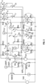
  • FIG 3 is a schematic diagram of one embodiment of an emitter resistance compensation circuit.
  • the emitter resistance compensation circuit includes two replica transistors (replicas of the logarithmic bipolar transistor NPN_LOG1 of Figure 2 ) with a large current density ratio driven by a scaled down copy of the input current compensated by the natural logarithm of the current density ratio multiplied by a thermal voltage.
  • a compensation signal I RE , in this example
  • the replica transistor's emitter resistance is matching the logging transistor's emitter resistance with a scaling factor, the accuracy of the compensation versus process and temperature is improved as compared to using a discrete resistor in the compensation circuit.
  • NPN_LOG1 is the same device in both Figures 2 and 3 .
  • NPN3 receives a collector current of I(INP)/32 plus a PTAT current 2 ⁇ I PTAT . Additionally, the current density in NPN3 is 4 times the current density in NPN_LOG1 at high input currents I(INP). Furthermore, NPN4 receives a collector current of I(INP)/64 plus a current I PTAT .
  • a PNP differential pair receives the NPN3 base-emitter voltage and the NPN4 base-emitter voltage + V R 4 as an input.
  • V N k ⁇ T q .
  • V N k ⁇ T q .
  • V N term 1 n + term 2 n + term 3 n.
  • rm 4 p ⁇ term 3 n 0.25 ⁇ R e ⁇ I PTAT + I INP 32 ⁇ 2 ⁇ R e ⁇ I PTAT + I INP 32
  • transistors T 15 to T 22 and resistors Rk, Rn and R 3 are for base current compensation. Additionally, the differential pair output current can drive the positive input of the amplifier OA1 of Figure 2 .
  • I Re I PTAT ⁇ tanh V P ⁇ V N 2 ⁇ V T for
  • ⁇ V T I Re ⁇ q ⁇ V P ⁇ V N 2 ⁇ k ⁇ T ⁇ I PTAT .
  • V OS ⁇ 7 16 ⁇ R e ⁇ I PTAT .
  • the offset will be -0.03dB. This offset is temperature independent as long as R e is temperature independent and can be reduced or eliminated by calibration.
  • the shared bias current of T 10 and T 11 can be chosen less than PTAT which reduces the effect of more pronounced peaking at cold and high input currents.
  • a new factor of -0.4375 ⁇ R e ⁇ I PTAT introduces an offset in dB of dBxos ⁇ ⁇ 1.9 ⁇ R e R 1 dB , which typically is small and can be eliminated by calibration.
  • I(INP) and I(IREF) may each vary over the full specified range of 1 nA to 10 mA.
  • the reference current is generated internally. It is defined as I REF if this current is internally generated.
  • I REF is trimmed for best VLOG vs I ( INP ) logarithmic conformance.
  • V Eref ⁇ E dBx ⁇ k ⁇ T ⁇ LN 10 20 ⁇ q [hereinafter Equation 2].
  • V Y is the log slope voltage (and, for the case of base-10 logarithms, it is also the volts per decade) and I INT is the extrapolated log X-axis intercept.
  • the emitter resistance compensation schemes herein correct errors in the input/output relation of a log-amp arising from emitter resistance.
  • RE2 doesn't introduce a significant error because the internal reference current is low enough not to affect V ( Eref - E ) much. If the reference current is sourced externally, for example in current-ratio applications, RE2 can introduce a significant error as well if I ( IREF ) is high.
  • FIG. 5 is a schematic diagram of one example of a bipolar differential pair, in which T1/T2 are equal area and T3/T4 are equal area.
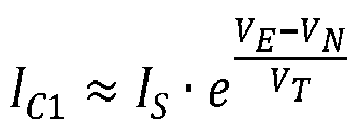
  • I C 1 ⁇ I S ⁇ e V E ⁇ V N V T and I C 2 ⁇ I S ⁇ e V E ⁇ V P V T for I C 1 , I C 2 ⁇ I S , where V T k ⁇ T q with Boltzmann's constant k, electron charge q and absolute temperature T.
  • I C 1 I S ⁇ e V E ⁇ V N V T and I C 2 ⁇ I S ⁇ e V E ⁇ V P V T for I C 1 , I C 2 ⁇ I S .
  • I C 1 I PTAT 1 + e V E ⁇ V N V T
  • I C 2 I PTAT 1 + e V P ⁇ V E V T .
  • V P ⁇ V N ⁇ V T I Re ⁇ V P ⁇ V N 2 ⁇ V T . I PTAT .
  • Figure 6 is a graph of one example of an emitter resistance compensation simulation. The simulation simulates one implementation of emitter resistance compensation for different temperature values. Simulations with and without emitter resistance compensation are enabled are shown.
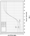
  • Figure 7 is a graph of one example of dVBE voltage change versus differential voltage V P - V N .
  • I PTAT k ⁇ T q ⁇ 4 ⁇ R 1 LN 8 and R 1 around OA1 in Figure 2 .
  • the dVBE output voltage change is independent with temperature.
  • the gain is chosen 0.25 because the current density of NPN3 is 4x the current density in NPN_LOG1.
  • An accurate compensation can be achieved up to 5mV dVBE.
  • With an emitter resistance RE1 of for example 1 ⁇ about up to 5mA can be compensated accurately.
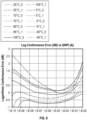
  • Figure 8 is a graph of one example of logarithmic conformance error versus input current.
  • the dashed line is with Re compensation off.
  • the graph uses a tail current for the differential pair T10 and T11 in Figure 3 with value closer to constant vs temperature (ZTAT) than PTAT.
  • Non-limiting aspect of the disclosure are set out in the following numbered clauses.

Landscapes

  • Engineering & Computer Science (AREA)
  • Power Engineering (AREA)
  • Physics & Mathematics (AREA)
  • Mathematical Physics (AREA)
  • Theoretical Computer Science (AREA)
  • Software Systems (AREA)
  • Computer Hardware Design (AREA)
  • General Physics & Mathematics (AREA)
  • Amplifiers (AREA)

Abstract

Logarithmic current-to-voltage converters with emitter resistance compensation are disclosed herein. In certain embodiments, a logarithmic current-to-voltage converter includes a logarithmic bipolar transistor that converts an input current to a logarithmic voltage, and an emitter resistance compensation circuit that includes a replica of the logarithmic bipolar transistor. The emitter resistance compensation circuit processes a copy of the input current to generate an emitter resistance compensation signal that adjusts the logarithmic voltage to correct for an error introduced by an emitter resistance of the logarithmic bipolar transistor. By providing emitter resistance compensation in this matter, logarithmic current-to-voltage conversion with high accuracy and low log error is achieved.

Description

    Field of the Disclosure
  • Embodiments of the invention relate to electronic systems, and more particularly to, electronic circuits for logarithmic conversion or detection.
  • BACKGROUND
  • Logarithmic converters or detectors provide an output signal that changes in relation to a logarithm of an applied input signal.
  • One type of logarithmic detector is a trans-linear logarithmic detector that uses the trans-linear properties of a bipolar transistor to provide logarithmic conversion. In one example, a collector and a base of an NPN bipolar transistor are directly connected to a gate and a source, respectively, of an n-type metal-oxide-semiconductor (NMOS) transistor. Additionally, an input current is applied to the collector of NPN bipolar transistor and the base of the NPN bipolar transistor generates a log voltage. Although such a circuit can provide logarithmic detection, the collector-to-base voltage of the NPN bipolar transistor is not very close to zero, leading to undesirable performance characteristics such as poor log-linear dynamic range for small input currents.
  • In another example of a trans-linear logarithmic detector, a collector and an emitter of an NPN bipolar transistor are directly connected to an inverting input and an output, respectively, of an operational amplifier (op-amp). Additionally, a base of the NPN bipolar transistor and a non-inverting input of the op-amp are grounded, while an input current is applied to the collector of NPN bipolar transistor such that the emitter of the NPN bipolar transistor generates a log voltage. By using the op-amp, the collector-to-base voltage of the NPN bipolar transistor can be controlled close to zero.
  • In certain applications, a second copy of a logarithmic detector is included and driven by a reference current, with a difference between the pair of logarithmic detectors taken to cancel the saturation current of the NPN bipolar transistor.
  • SUMMARY OF THE DISCLOSURE
  • Logarithmic current-to-voltage converters with emitter resistance compensation are disclosed herein. In certain embodiments, a logarithmic current-to-voltage converter includes a logarithmic bipolar transistor that converts an input current to a logarithmic voltage, and an emitter resistance compensation circuit that includes a replica of the logarithmic bipolar transistor. The emitter resistance compensation circuit processes a copy of the input current to generate an emitter resistance compensation signal that adjusts the logarithmic voltage to correct for an error introduced by an emitter resistance of the logarithmic bipolar transistor. By providing emitter resistance compensation in this matter, logarithmic current-to-voltage conversion with high accuracy and low log error is achieved.
  • In one aspect, a logarithmic current to voltage converter includes an input terminal configured to receive an input current, a logarithmic bipolar transistor having a collector connected to the input terminal and an emitter configured to generate a logarithmic output voltage, and an emitter resistance compensation circuit comprising a replica of the logarithmic bipolar transistor. The emitter resistance compensation circuit is configured to receive a copy of the input current and to generate a compensation signal operable to adjust the logarithmic voltage to correct for an error arising from an emitter resistance of the logarithmic bipolar transistor.
  • In another aspect, a photocurrent detection system includes a photodetector configured to generate an input current, and a semiconductor die including a logarithmic converter. The logarithmic converter includes an input terminal configured to receive the input current, a logarithmic bipolar transistor having a collector connected to the input terminal and an emitter configured to generate a logarithmic output voltage, and an emitter resistance compensation circuit comprising a scaled replica of the logarithmic bipolar transistor. The emitter resistance compensation circuit is configured to receive a scaled copy of the input current and to generate a compensation signal operable to adjust the logarithmic voltage to correct for an error arising from an emitter resistance of the logarithmic bipolar transistor.
  • In another aspect, a method of logarithmic current to voltage conversion is provided. The method includes providing an input current from an input terminal to a collector of a bipolar transistor, providing a logarithmic output voltage from an emitter of the logarithmic bipolar transistor, and generating a compensation signal using an emitter resistance compensation circuit that includes a scaled replica of the logarithmic bipolar transistor. Generating the compensation circuit includes receiving a scaled copy of the input current as an input to the emitter resistance compensation circuit and adjusting the logarithmic voltage to correct for an error arising from an emitter resistance of the logarithmic bipolar transistor using the compensation signal.
  • BRIEF DESCRIPTION OF THE DRAWINGS
    • Figure 1A is a schematic diagram of one embodiment of a logarithmic converter.
    • Figure 1B is a schematic diagram of one embodiment of a logarithmic conversion system.
    • Figure 2 is a schematic diagram of one embodiment of a logarithmic conversion system with emitter resistance compensation.
    • Figure 3 is a schematic diagram of one embodiment of an emitter resistance compensation circuit.
    • Figure 4 is a graph of one example of logarithmic output voltage versus input current.
    • Figure 5 is a schematic diagram of one example of a bipolar differential pair.
    • Figure 6 is a graph of one example of an emitter resistance compensation simulation.
    • Figure 7 is a graph of one example of base-to-emitter voltage change versus differential voltage.
    • Figure 8 is a graph of one example of logarithmic conformance error versus input current.
    DETAILED DESCRIPTION
  • The following detailed description of embodiments presents various descriptions of specific embodiments of the invention. However, the invention can be embodied in a multitude of different ways. In this description, reference is made to drawings. It will be understood that elements illustrated in the figures are not necessarily drawn to scale. Moreover, it will be understood that certain embodiments can include more elements than illustrated in a drawing and/or a subset of the elements illustrated in a drawing. Further, some embodiments can incorporate any suitable combination of features from two or more drawings.
  • Figure 1A is a schematic diagram of one embodiment of a logarithmic converter 105.
  • In the illustrated embodiment, the logarithmic converter 105 includes a FET transistor (NMOS, in this example), a first bipolar transistor NPN_LOG (n-type, in this example), a second bipolar transistor NPN_LV (n-type, in this example), a first DC current source IDC1, a second DC current source IDC2, a capacitor C, and a resistor R.
  • The NMOS transistor includes a drain that receives a power supply voltage +Vc, and a gate connected to a collector of the first bipolar transistor NPN_LOG and to an input terminal. The input terminal receives an input current IIN and has an input voltage VIN. The NMOS transistor further includes a source connected to a base of the second bipolar transistor NPN_LV and to the first DC current source IDC1. Additionally, a base of the first bipolar transistor NPN_LOG receives a reference voltage VREF and an emitter of the first bipolar transistor NPN_LOG is connected to an output terminal that provides a logarithmic voltage VLOG. The emitter of the first bipolar transistor NPN_LOG is also connected to the second DC current source IDC2 and to a collector of the second bipolar transistor NPN_LV. The resistor R is connected between an emitter of the second bipolar transistor NPN_LV and ground, and the capacitor C is connected in parallel with the resistor R.
  • As shown in Figure 1A, the input current IIN received from the input terminal is provided to the collector of the first bipolar transistor NPN_LOG. Additionally, the logarithmic converter 105 converts the input current IIN into the logarithmic voltage VLOG, which is provided at the output terminal.
  • In the illustrated embodiment, the capacitor C operates to extend the bandwidth of the collector current over base voltage while the resistor R reduces the loop gain at high levels of the input current IIN. In certain implementations, the capacitor C and/or the resistor R are controllable (for example, by using a capacitor array that is programmable to control a capacitance value and/or a resistor array that is programmable to control a resistance value).
  • The logarithmic converter 105 can achieve a higher speed relative to a configuration using an op-amp to provide feedback. For example, when an op-amp is included in the feedback loop, the additional components introduce extra phase shift that moves the second-order pole downwards in frequency. Although high value compensation capacitors can be added to keep such a feedback loop stable, high capacitance slows the circuit down.
  • Furthermore, the logarithmic converter 105 has superior noise performance at low levels of the input current IIN relative to an implementation with an op-amp in the feedback loop. For example, when an op-amp provides feedback at low input current levels, the bandwidth of the circuit reduces considerably, resulting in the loop gain to drop below 0dB at a frequency below the baseband bandwidth of the rest of the circuit. This results in the loop not cancelling the bias noise sources in a significant manner. In that case, any noise voltage present on the reference voltage will be amplified significantly by the op-amp.
  • In contrast, any noise on the reference voltage VREF in Figure 1A will be amplified much less since the amplification at the base of the first bipolar transistor NPN_LOG (which is connected as a common-base stage) is much lower.
  • Figure 1B is a schematic diagram of one embodiment of a logarithmic conversion system 120. The logarithmic conversion system 120 includes a first logarithmic converter 105a, a second logarithmic converter 105b, a reference current source IREF, and a reference voltage source 106 that includes a third logarithmic converter 105c, a DC current source IDC, a reference voltage source VREF2, an adder 111, an offset trim circuit 112, and a buffer 113. The logarithmic conversion system 120 is also depicted with an input current source IIN, which represents a photodiode or other input current source to the system 120.
  • As shown in Figure 1B, multiple instantiations or replicas of the logarithmic converter 105 of Figure 1A have been arranged to provide logarithmic current to voltage conversion with enhanced performance. In particular, the first logarithmic converter 105a serves as an input channel, the second logarithmic converter 105b serves as a reference channel, and the third logarithmic converter 105c serves as a DC channel.
  • In the illustrated embodiment, the DC current from the DC current source IDC is provided as an input to the third logarithmic converter 105c, which is biased by the reference voltage source VREF2. Additionally, the buffer 113 buffers the input voltage to the third logarithmic converter 105c. The buffered voltage from the buffer 113 is trimmed by the offset trim circuit 112 to generate a reference voltage VREF for the first logarithmic converter 105a and the second logarithmic converter 105b.
  • By implementing the logarithmic conversion system 120 in this manner, high dynamic range is achieved by setting the voltage reference VREF in such a manner that the collector-to-emitter voltages (of bipolar transistors NPN_LOG within the converters 105a and 15b) are close to zero. In particular, the logarithmic conversion system 120 applies a DC current to the third logarithmic converter 105c, which is biased with the reference voltage source VREF2. The precision of the reference voltage source VREF2 can be relaxed compared to a precision of the reference voltage VREF since the DC current from the DC current source IDC can be scaled to be much higher than a minimum value of the input current IIN.
  • With continuing reference to Figure 1B, the input channel (the first logarithmic converter 105a), the reference channel (the second logarithmic converter 105b), and the DC channel (the third logarithmic converter 105c) can be scaled in size to provide enhanced performance. In one implementation, the input channel and the reference channel have a scaling factor 8 while the DC channel has a scaling factor 2. Although one example of scaling factors is provided, other scaling factors can be used.
  • Since the DC current from the DC current source IDC can be chosen to be in the middle of the dynamic range of the input current source IIN (for instance, 100µA), larger deviations around zero of the collector-base voltage of bipolar transistor NPN_LOG has little to no impact on accuracy.
  • As shown in Figure 1B, the log voltage VLOG2 is taken differentially between the VLOG outputs of the first logarithmic converter 105a and the second logarithmic converter 105b. By using a differential voltage between the input channel and the reference channel, the saturation current of the bipolar transistors (NPN_LOG transistors within converters 105a and 105b) is canceled.
  • In the illustrated embodiment, the buffer 113 is a voltage buffer with unity gain (+1). The buffer 113 is applied to the input voltage of the DC channel to bias the input and reference channels (VREF voltages). The offset trim circuit 112 can be used to correct for mismatches and/or for the difference between the DC current in the DC channel and the lowest input current in the input channel.
  • Moreover, in certain embodiments, the offset trim circuit 112 applies a correction voltage, such as a proportional to temperature (PTAT) voltage (for instance, around 50mV) which is added to the reference voltage VREF to correct for low input current IIN and/or high temperature deviations.
  • Absent compensation, the logarithmic conversion circuits of Figures 1A and 1B can suffer from logarithmic error introduced by the emitter resistance (RE) of the transistor used for logarithmic current-to-voltage conversion.
  • For example, an optical log converter uses the logarithmic relationship between the base-emitter voltage (VBE) and the collector current (IC) of a bipolar junction transistor. Additionally, a log amp that employs this property of a bipolar transistor is referred to as a logarithmic trans-impedance amplifier.
  • With reference back to Figures 1A and 1B, the bipolar transistor of an input channel (the first logarithmic converter 105a of Figure 1B) can have a first emitter resistance RE1, and the bipolar transistor of a reference channel (the second logarithmic converter 105b of Figure 1B) can have a second emitter resistance RE2. If RE1 ≠ 0 and RE2 ≠ 0 an error is introduced causing the VLOG curve to change at the higher end of the input current range.
  • Logarithmic current-to-voltage converters with emitter resistance compensation are disclosed herein. In certain embodiments, a logarithmic current-to-voltage converter includes a logarithmic bipolar transistor that converts an input current to a logarithmic voltage, and an emitter resistance compensation circuit that includes a replica of the logarithmic bipolar transistor. The emitter resistance compensation circuit processes a copy of the input current to generate an emitter resistance compensation signal that adjusts the logarithmic voltage to correct for an error introduced by an emitter resistance of the logarithmic bipolar transistor.
  • By providing emitter resistance compensation in this matter, logarithmic current-to-voltage conversion with high accuracy and low log error is achieved.
  • Figure 2 is a schematic diagram of one embodiment of a logarithmic conversion system 130 with emitter resistance compensation. The logarithmic conversion system 130 includes an input channel 125a (receiving an input current I(INP)), a reference chancel 125b, a reference voltage source VREF, a reference current source IREF (provided to the reference channel 125b), and an output amplifier (OA1, which can be an operational amplifier) for processing a differential logarithmic voltage provided across the output nodes (E and Eref) of the input channel 125a and the reference chancel 125b.
  • The output amplifier OA1 is biased by various current sources (IB1, IB2, and IPTLS+IRe) as shown, and includes input resistors (of resistance R1) at each of the positive and negative inputs, a feedback resistor (of resistance R1) from output to negative input, and a bias resistor (of resistance R1) from the positive input to ground. The output amplifier OA1 serves to output the difference voltage between E and Eref plus an offset to generate a unipolar logarithmic signal, which in certain implementations is processed by an analog temperature compensation circuit to compensate for absolute temperature T.
  • The input channel 125a and the reference channel 125b have a configuration similar to that of Figure 1A, except that particular example resistance values are depicted and the parasitic emitter resistances of the bipolar transistors NPN_LOG1 and NPN_LOG2 are shown. In particular, the input channel 125a includes logarithmic bipolar transistor NPN_LOG1 with a first emitter resistance RE1, while the reference channel 125b includes reference bipolar transistor NPN_LOG2 with a second emitter resistance RE2.
  • If RE1 ≠ 0 and RE2 ≠ 0 an error is introduced causing the VLOG curve to change at the higher end of the input current range. This is caused by a voltage drop over RE1 that lowers the E node voltage at high input currents and thus increases V(Eref - E) by a value of VRe = RE1 · I(INP). Typically, RE2 doesn't introduce a significant error because the internal reference current is sufficiently low not to affect V(Eref - E) much. However, if the reference current is sourced externally, for example in current-ratio applications, RE2 can introduce a significant error as well if I(IREF) is high.
  • The logarithmic conversion system 130 includes the emitter resistance compensation circuit 126 to compensate for this effect. In the illustrated embodiment, the emitter resistance compensation circuit 126 includes a scaled replica or copy of the logarithmic bipolar transistor NPN_LOG1. The scaled replica processes a copy 127 of the input current (IINP), which can be scaled down in value to reduce power dissipation. The emitter resistance compensation circuit 126 processes the input current copy 127 to generate an emitter resistance compensation signal for compensating the logarithmic voltage of the logarithmic conversion system 130.
  • In the illustrated embodiment, the emitter resistance compensation signal corresponds to a correction current IRE that is provided to a positive input of the output amplifier OA1 to provide a correction to the logarithmic voltage. However, other types of correction signal schemes can be used.
  • Any suitable circuit (for example, any suitable current mirror) can provide the scaled replica of the input current to the emitter resistance compensation circuit 126.
  • Figure 3 is a schematic diagram of one embodiment of an emitter resistance compensation circuit. In this example, the emitter resistance compensation circuit includes two replica transistors (replicas of the logarithmic bipolar transistor NPN_LOG1 of Figure 2) with a large current density ratio driven by a scaled down copy of the input current compensated by the natural logarithm of the current density ratio multiplied by a thermal voltage. By implementing the emitter resistance compensation circuit in this manner, a compensation signal (IRE, in this example) proportional with the emitter resistance times the input current is generated.
  • Because the replica transistor's emitter resistance is matching the logging transistor's emitter resistance with a scaling factor, the accuracy of the compensation versus process and temperature is improved as compared to using a discrete resistor in the compensation circuit.
  • Thus, a lower scaled copy of the input current I(INP) is provided by the collector current of NPN_MON1. NPN_LOG1 is the same device in both Figures 2 and 3.
  • The circles in Figure 3 indicate that the emitter resistance (fraction) is part of the transistor itself, not a separate component.
  • NPN3 receives a collector current of I(INP)/32 plus a PTAT current 2 · IPTAT. Additionally, the current density in NPN3 is 4 times the current density in NPN_LOG1 at high input currents I(INP). Furthermore, NPN4 receives a collector current of I(INP)/64 plus a current IPTAT.
  • With continuing reference to Figure 3, a PTAT voltage V R4 equal to the natural logarithm of the ratio of the current densities of NPN3 and NPN4 times a thermal voltage V T = k T q
    Figure imgb0001
    is added to the NPN4 base-emitter voltage.
  • Furthermore, a PNP differential pair receives the NPN3 base-emitter voltage and the NPN4 base-emitter voltage + V R4 as an input.
  • The PTAT current is given by: I PTAT = k T q 4 R 1 LN A
    Figure imgb0002
    with A=8 the emitter ratio and 4 · R 1 the resistor that sets the current in the bandgap of the PTAT current generator.
  • For I(INP)=0 the differential pair input voltage VN is given by V N = k T q .
    Figure imgb0003
    LN I INP 16 + 2 I PTAT I S + R e 2 I PTAT + I INP 16
    Figure imgb0004
    . This can be expressed as V N = k T q .
    Figure imgb0005
    LN I INP 16 + 2 I PTAT 4 I S + k T q LN 4 + 2 R e I PTAT + I INP 32
    Figure imgb0006
    , or VN = term1n + term2n + term3n.
  • Assuming base currents for T 10 and T 11 are zero, the voltage drop over R 4 is V R 4 = I PTAT R 4 = k T q 4 R 1 LN 8 4 R 1 = k T q LN 8
    Figure imgb0007
    . For I(INP)=0 the differential pair input voltage VP is given by V P = k T q LN I INP 32 + I PTAT 4 I S + k T q LN 8 + 0.25 R e ( I PTAT +
    Figure imgb0008
    I INP 32 )
    Figure imgb0009
    . This can be expressed as V P = k T q LN I INP 16 + 2 I PTAT 4 I S + k T q LN 0.5 +
    Figure imgb0010
    k T q LN A + 0.25 R e I PTAT + I INP 32
    Figure imgb0011
    or VP = term1p + term2p + term3p + term4p, where term1p - term1n = 0.
  • With continuing reference to Figure 3, term2p + term3p - term 2 n = k T q LN 0.5 + k T q LN 8 k T q LN 4 = k T q LN 1 = 0
    Figure imgb0012
    . Additionally, rm 4 p term 3 n = 0.25 R e I PTAT + I INP 32 2 R e I PTAT + I INP 32
    Figure imgb0013
    , and V P V N = term 4 p term 3 n = 1.75 R e I PTAT + I INP 32 .
    Figure imgb0014
  • Accordingly, transistors T 15 to T 22 and resistors Rk, Rn and R 3 are for base current compensation. Additionally, the differential pair output current can drive the positive input of the amplifier OA1 of Figure 2.
  • The output voltage of the input stage and level shifter with Re = 64· RE1 is given by dVBE = V Eref E + I INP R e 64 + I Re R 1 + I PTLS 0 T T 0 R 1
    Figure imgb0015
    , where I PTLS0 is the PTAT level-shift current IPTLS at temperature T = T 0 and Re = 64 · RE1 and RE2 · I(IREF)≪1mV.
  • Furthermore, I Re = I PTAT tanh V P V N 2 V T
    Figure imgb0016
    for |VN - VP | < VT : IRe q V P V N 2 k T I PTAT
    Figure imgb0017
    . Additionally, I PTAT = k T q 4 R 1 LN 8 k T q 2 R 1
    Figure imgb0018
    and I Re q V P V N 2 k T k T q 2 R 1 =
    Figure imgb0019
    V P V N 4 R 1
    Figure imgb0020
    .
  • With continuing reference to Figure 3, VP - VN = -1.75 · Re · I PTAT + I INP 32 = 1.75 R e I PTAT 7 128 R e I INP
    Figure imgb0021
    . Additionally, IRe · R 1 = V P V N 4 = 7 16 R e I PTAT + I INP 32 = 7 16 R e I PTAT 7 512 R e I INP
    Figure imgb0022
    and I INP R e 64 + I Re R 1 = 8 512 7 512 R e I INP 0.4375 R e I PTAT
    Figure imgb0023
    .
  • Thus, with emitter resistance compensation I INP R e 64 + I Re R 1 =
    Figure imgb0024
    8 512 7 512 R e I INP 0.4375 R e I PTAT
    Figure imgb0025
    , and dVBE = V(Eref - E) + 1 512 R e I INP 0.4375 R e I PTAT + I PTLS 0 T T 0 R 1
    Figure imgb0026
    . Compared to dVBE without compensation, error due to Re is reduced by a factor of 512/64=8.
  • With reference to Figures 2 and 3, without emitter resistance compensation, the input stage output voltage of Figure 2 is given by dVBE = V Eref E + 1 64 R e
    Figure imgb0027
    I INP + I PTLS 0 T T 0 R 1
    Figure imgb0028
    .
  • Due to the Re compensation, an offset is introduced with value V OS = 7 16 R e I PTAT .
    Figure imgb0029
  • Additionally, dBx = 20 Log 10 I INP I IREF = 20 q k T LN 10 V Eref E
    Figure imgb0030
    and I PTAT = k T q 4 R 1 LN 8 k T q 2 R 1 = > V OS = 7 16 R e k T q 2 R 1
    Figure imgb0031
    . A dB value dBxos can be assigned to this offset to be dBxos = 20 q k T Ln 10 7 16 k T q 2 R 1 R E = 35 8 LN 10 R e R 1 1.9 R e R 1
    Figure imgb0032
    . For typical values for Re = 64 and R 1 = 4000, the offset will be -0.03dB. This offset is temperature independent as long as Re is temperature independent and can be reduced or eliminated by calibration.
  • Moreover, by changing the shared bias current of T 10 and T 11 from IPTAT to 16 7 LN 8 I PTAT 1.1 I PTAT
    Figure imgb0033
    , the Re · I(INP) term would be zero. The shared bias current of T 10 and T 11 can be chosen less than PTAT which reduces the effect of more pronounced peaking at cold and high input currents.
  • By including the emitter resistance compensation circuit of Figure 3, the output voltage of the input stage of Figure 2 is now given by dVBE = V(Eref - E) + 1 512 R e I INP 0.4375 R e I PTAT + I PTLS 0 T T 0 R 1
    Figure imgb0034
    . Accordingly, the error introduced by emitter resistance is decreased by a factor of 8.
  • Moreover, a new factor of -0.4375 · Re · IPTAT introduces an offset in dB of dBxos 1.9 R e R 1 dB
    Figure imgb0035
    , which typically is small and can be eliminated by calibration.
  • With reference back to Figure 2, we can define dBx = 20 · with dBx the ratio in dB between I(INP) and I(IREF), assuming RE1 = 0 and RE2 = 0 and LN(x) = Loge (x).
  • In log ratio applications, both I(INP) and I(IREF) may each vary over the full specified range of 1 nA to 10 mA. However, in default operation, the reference current is generated internally. It is defined as IREF if this current is internally generated. IREF is trimmed for best VLOG vs I(INP) logarithmic conformance. Thus, V Eref E = dBx k T LN 10 20 q
    Figure imgb0036
    [hereinafter Equation 2].
  • Equation 2 shows that the V(Eref - E) is still proportional-to-absolute-temperature (PTAT) and temperature variation of k T q
    Figure imgb0037
    is subsequently eliminated by temperature compensation circuitry that essentially puts a variable proportional to absolute temperature underneath the T in Equation 2 and raising the magnitude to a stable value of 10mV/dB or 200mV/decade. Therefore, for photodiode applications, using this correction the relationship between a photodiode current, IPD, applied to the INP pin, and the voltage appearing at the output at VLOG is given by VLOG = V Y Log 10 I PD I INT
    Figure imgb0038
    [hereinafter Equation 3]. Here, VY is the log slope voltage (and, for the case of base-10 logarithms, it is also the volts per decade) and IINT is the extrapolated log X-axis intercept.
  • The output at VLOG can also be expressed as VLOG = 0.01 · dBx = 0.2 q k T LN 10 V Eref E
    Figure imgb0039
    [hereinafter Equation 4]. The relationship between VY and V(Eref - E) is 3.33 at T=302.4K in the default configuration. For a factor of 10 between I(INP) and IREF, V(Eref - E) = 60mV at T=302.4K, resulting in a slope of 0.2 V/decade.
  • In certain implementations, during fabrication, VY is set to 0.2 V/decade (10 mV/dB) and IINT = 10pA by factory trim.
  • The output at VLOG can further be expressed as VLOG = 0.2 V · . The output for the value of IPD can be calculated using Equation 5. For example, for IPD = 10 nA, the output VLOG has a value of 0.6 V. When IPD = 100 pA, the output VLOG has a value of 0.2 V.
  • Figure 4 is a graph of one example of logarithmic output voltage versus input current. The graph shows the input/output relation of an ideal log-amp. Horizontal scale is logarithmic and spans a wide dynamic range. Output passes through zero at IINP = IINT.
  • The emitter resistance compensation schemes herein correct errors in the input/output relation of a log-amp arising from emitter resistance.
  • For example, if RE1 ≠ 0 and RE2 ≠ 0 , an error is introduced causing the VLOG curve to change at the higher end of the input current range. This is caused by a voltage drop over RE1 that lowers the 'E' node voltage at high input currents and thus increases V(Eref - E) by a value of V Re = 1 64 R e I INP
    Figure imgb0040
    , with Re = 64 · RE1. Thus, dVBE = V Eref E + 1 64 R e I INP + I PTLS 0 T T 0 R 1
    Figure imgb0041
    [hereinafter Equation 6].
  • Typically, RE2 doesn't introduce a significant error because the internal reference current is low enough not to affect V(Eref - E) much. If the reference current is sourced externally, for example in current-ratio applications, RE2 can introduce a significant error as well if I(IREF) is high.
  • From Equation 1 above, at T=302.4K the logarithmic error is 0.333 dB/mV drop over RE1.
  • Figure 5 is a schematic diagram of one example of a bipolar differential pair, in which T1/T2 are equal area and T3/T4 are equal area.
  • With reference to Figure 5, I C 1 I S e V E V N V T
    Figure imgb0042
    and I C 2 I S e V E V P V T
    Figure imgb0043
    for I C1 , I C2IS, where V T = k T q
    Figure imgb0044
    with Boltzmann's constant k, electron charge q and absolute temperature T.
  • Thus, I C 1 I S e V E V N V T
    Figure imgb0045
    and I C 2 I S e V E V P V T
    Figure imgb0046
    for I C1 , I C2IS. Additionally, IC1 + I C2 = IPTAT and I C1 - I C2 = IRe, I C 1 = I PTAT 1 + e V E V N V T
    Figure imgb0047
    and I C 2 = I PTAT 1 + e V P V E V T
    Figure imgb0048
    .
  • Furthermore, I Re = I PTAT e V P V N V T 1 e V P V N V T + 1 = I PTAT tanh V P V N 2 V T
    Figure imgb0049
    , and d dx tanh x = 1 cosh 2 x
    Figure imgb0050
    for x = 0 , 1 cosh 2 x = 1
    Figure imgb0051
    . For V P V N < V T : I Re V P V N 2 V T .
    Figure imgb0052
    IPTAT.
  • Figure 6 is a graph of one example of an emitter resistance compensation simulation. The simulation simulates one implementation of emitter resistance compensation for different temperature values. Simulations with and without emitter resistance compensation are enabled are shown.
  • Figure 7 is a graph of one example of dVBE voltage change versus differential voltage VP - VN. The graph uses a PTAT tail current for the differential pair T10 and T11 in Figure 3 with value I PTAT = k T q 4 R 1 LN 8
    Figure imgb0053
    and R 1 around OA1 in Figure 2. For small input voltages for the T10 & T11 differential pair up to 20mV, the dVBE output voltage change is independent with temperature. The gain is chosen 0.25 because the current density of NPN3 is 4x the current density in NPN_LOG1. An accurate compensation can be achieved up to 5mV dVBE. With an emitter resistance RE1 of for example 1Ω, about up to 5mA can be compensated accurately.
  • Figure 8 is a graph of one example of logarithmic conformance error versus input current. The dashed line is with Re compensation off. The graph uses a tail current for the differential pair T10 and T11 in Figure 3 with value closer to constant vs temperature (ZTAT) than PTAT.
  • As shown in Figure 8, the difference between Re Compensation On and Off is larger at cold temperature. Additionally, Re Compensation is not cause of downward slope at -40°C.
  • Conclusion
  • The foregoing description may refer to elements or features as being "connected" or "coupled" together. As used herein, unless expressly stated otherwise, "connected" means that one element/feature is directly or indirectly connected to another element/feature, and not necessarily mechanically. Likewise, unless expressly stated otherwise, "coupled" means that one element/feature is directly or indirectly coupled to another element/feature, and not necessarily mechanically. Thus, although the various schematics shown in the figures depict example arrangements of elements and components, additional intervening elements, devices, features, or components may be present in an actual embodiment (assuming that the functionality of the depicted circuits is not adversely affected).
  • While certain embodiments have been described, these embodiments have been presented by way of example only, and are not intended to limit the scope of the disclosure. Indeed, the novel apparatus, methods, and systems described herein may be embodied in a variety of other forms; furthermore, various omissions, substitutions and changes in the form of the methods and systems described herein may be made without departing from the spirit of the disclosure. For example, while the disclosed embodiments are presented in a given arrangement, alternative embodiments may perform similar functionalities with different components and/or circuit topologies, and some elements may be deleted, moved, added, subdivided, combined, and/or modified. Each of these elements may be implemented in a variety of different ways. Any suitable combination of the elements and acts of the various embodiments described above can be combined to provide further embodiments. Accordingly, the scope of the present invention is defined only by reference to the appended claims.
  • Although the claims presented here are in single dependency format for filing at the USPTO, it is to be understood that any claim may depend on any preceding claim of the same type except when that is clearly not technically feasible.
  • ASPECT OF THE DISCLOSURE
  • Non-limiting aspect of the disclosure are set out in the following numbered clauses.
    1. 1. A logarithmic current to voltage converter comprising:
      • an input terminal configured to receive an input current;
      • a logarithmic bipolar transistor having a collector connected to the input terminal and an emitter configured to generate a logarithmic output voltage; and
      • an emitter resistance compensation circuit comprising a replica of the logarithmic bipolar transistor, wherein the emitter resistance compensation circuit is configured to receive a copy of the input current and to generate a compensation signal operable to adjust the logarithmic voltage to correct for an error arising from an emitter resistance of the logarithmic bipolar transistor.
    2. 2. The logarithmic current to voltage converter of Clause 1, wherein the compensation signal is proportional to the emitter resistance.
    3. 3. The logarithmic current to voltage converter of any preceding Clause, wherein the emitter resistance compensation circuit comprises a pair of bipolar transistors configured to sense a difference voltage that changes based on the emitter resistance of the logarithmic bipolar transistor times a scaled copy of the input current.
    4. 4. The logarithmic current to voltage converter of Clause 3, wherein the difference voltage is sensed between a pair of scaled replica transistors with a current density ratio of at least four to one.
    5. 5. The logarithmic current to voltage converter of Clause 4, wherein the difference voltage is corrected by a voltage that is proportional to a natural logarithm of the current density ratio times a thermal voltage.
    6. 6. The logarithmic current to voltage converter of any of Clauses 3 to 5, wherein the pair of bipolar transistors is biased by a current that is proportional to absolute temperature (PTAT).
    7. 7. The logarithmic current to voltage converter of any preceding Clause, wherein the copy of the input current is scaled down in size relative to the input current.
    8. 8. The logarithmic current to voltage converter of any preceding Clause, wherein the replica of the logarithmic bipolar transistor is scaled down in size relative to the logarithmic bipolar transistor.
    9. 9. The logarithmic current to voltage converter of any preceding Clause, further comprising a logarithmic bipolar transistor having a collector configured to receive a reference current, wherein the logarithmic output voltage is taken differentially between the emitter of logarithmic bipolar transistor receiving the input current and an emitter of the logarithmic bipolar transistor receiving the reference current.
    10. 10. The logarithmic current to voltage converter of Clause 9, further comprising an output amplifier configured to receive the logarithmic output voltage between a first input and a second input.
    11. 11. The logarithmic current to voltage converter of Clause 9 or Clause 10, wherein the compensation signal is a compensation current provided to the first input of the output amplifier.
    12. 12. The logarithmic current to voltage converter of any preceding Clause, further comprising a bipolar transistor having a collector connected to the emitter of the logarithmic bipolar transistor.
    13. 13. The logarithmic current to voltage converter of Clause 12, further comprising a resistor connected between an emitter of the bipolar transistor and a ground voltage.
    14. 14. The logarithmic current to voltage converter of Clause 12 or Clause 13, further comprising a field-effect transistor having a gate connected to the collector of the logarithmic bipolar transistor and a source connected to a base of the bipolar transistor.
    15. 15. The logarithmic current to voltage converter of any preceding Clause, further comprising an input current source that generates the input current.
    16. 16. A photocurrent detection system comprising:
      • a photodetector configured to generate an input current; and
      • a semiconductor die comprising a logarithmic converter, wherein the logarithmic converter comprises:
        • an input terminal configured to receive the input current;
        • a logarithmic bipolar transistor having a collector connected to the input terminal and an emitter configured to generate a logarithmic output voltage; and
        • an emitter resistance compensation circuit comprising a scaled replica of the logarithmic bipolar transistor, wherein the emitter resistance compensation circuit is configured to receive a scaled copy of the input current and to generate a compensation signal operable to adjust the logarithmic voltage to correct for an error arising from an emitter resistance of the logarithmic bipolar transistor.
    17. 17. The photocurrent detection system of Clause 16, wherein the compensation signal is proportional to the emitter resistance.
    18. 18. The photocurrent detection system of Clause 16 or Clause 17, wherein the emitter resistance compensation circuit comprises a pair of bipolar transistors configured to sense a difference voltage that changes based on the emitter resistance of the logarithmic bipolar transistor times a scaled copy of the input current.
    19. 19. A method of logarithmic current to voltage conversion, the method comprising:
      • providing an input current from an input terminal to a collector of a bipolar transistor;
      • providing a logarithmic output voltage from an emitter of the logarithmic bipolar transistor; and
      • generating a compensation signal using an emitter resistance compensation circuit that comprises a scaled replica of the logarithmic bipolar transistor, including receiving a scaled copy of the input current as an input to the emitter resistance compensation circuit, and adjusting the logarithmic voltage to correct for an error arising from an emitter resistance of the logarithmic bipolar transistor using the compensation signal.
    20. 20. The method of Clause 19, wherein the compensation signal is proportional to the emitter resistance.

Claims (15)

  1. A logarithmic current to voltage converter comprising:
    an input terminal configured to receive an input current;
    a logarithmic bipolar transistor having a collector connected to the input terminal and an emitter configured to generate a logarithmic output voltage; and
    an emitter resistance compensation circuit comprising a replica of the logarithmic bipolar transistor, wherein the emitter resistance compensation circuit is configured to receive a copy of the input current and to generate a compensation signal operable to adjust the logarithmic voltage to correct for an error arising from an emitter resistance of the logarithmic bipolar transistor.
  2. The logarithmic current to voltage converter of Claim 1, wherein the compensation signal is proportional to the emitter resistance.
  3. The logarithmic current to voltage converter of any preceding Claim, wherein the emitter resistance compensation circuit comprises a pair of bipolar transistors configured to sense a difference voltage that changes based on the emitter resistance of the logarithmic bipolar transistor times a scaled copy of the input current.
  4. The logarithmic current to voltage converter of Claim 3, wherein the difference voltage is sensed between a pair of scaled replica transistors with a current density ratio of at least four to one,
    and wherein optionally the difference voltage is corrected by a voltage that is proportional to a natural logarithm of the current density ratio times a thermal voltage..
  5. The logarithmic current to voltage converter of Claims 3 or Claim 4, wherein the pair of bipolar transistors is biased by a current that is proportional to absolute temperature (PTAT).
  6. The logarithmic current to voltage converter of any preceding Claim, wherein at least one of the following applies:
    (a) the copy of the input current is scaled down in size relative to the input current;
    (b) the replica of the logarithmic bipolar transistor is scaled down in size relative to the logarithmic bipolar transistor.
  7. The logarithmic current to voltage converter of any preceding Claim, further comprising a logarithmic bipolar transistor having a collector configured to receive a reference current, wherein the logarithmic output voltage is taken differentially between the emitter of logarithmic bipolar transistor receiving the input current and an emitter of the logarithmic bipolar transistor receiving the reference current.
  8. The logarithmic current to voltage converter of Claim 8, further comprising an output amplifier configured to receive the logarithmic output voltage between a first input and a second input.
  9. The logarithmic current to voltage converter of Claim 8 or Claim 9, wherein the compensation signal is a compensation current provided to the first input of the output amplifier.
  10. The logarithmic current to voltage converter of any preceding Claim, further comprising a bipolar transistor having a collector connected to the emitter of the logarithmic bipolar transistor.
  11. The logarithmic current to voltage converter of Claim 10, further comprising a resistor connected between an emitter of the bipolar transistor and a ground voltage.
  12. The logarithmic current to voltage converter of Claim 10 or Claim 11, further comprising a field-effect transistor having a gate connected to the collector of the logarithmic bipolar transistor and a source connected to a base of the bipolar transistor.
  13. The logarithmic current to voltage converter of any preceding Claim, further comprising an input current source that generates the input current.
  14. A photocurrent detection system comprising:
    a photodetector configured to generate an input current; and
    a semiconductor die comprising the logarithmic current to voltage converter of any preceding claim.
  15. A method of logarithmic current to voltage conversion, the method comprising:
    providing an input current from an input terminal to a collector of a bipolar transistor;
    providing a logarithmic output voltage from an emitter of the logarithmic bipolar transistor; and
    generating a compensation signal using an emitter resistance compensation circuit that comprises a scaled replica of the logarithmic bipolar transistor, including receiving a scaled copy of the input current as an input to the emitter resistance compensation circuit, and adjusting the logarithmic voltage to correct for an error arising from an emitter resistance of the logarithmic bipolar transistor using the compensation signal.
EP24152364.6A 2023-01-24 2024-01-17 Logarithmic current to voltage converters with emitter resistance compensation Pending EP4407509A1 (en)

Applications Claiming Priority (2)

Application Number Priority Date Filing Date Title
US202363481266P 2023-01-24 2023-01-24
US18/410,182 US20240250647A1 (en) 2023-01-24 2024-01-11 Logarithmic current to voltage converters with emitter resistance compensation

Publications (1)

Publication Number Publication Date
EP4407509A1 true EP4407509A1 (en) 2024-07-31

Family

ID=89620667

Family Applications (1)

Application Number Title Priority Date Filing Date
EP24152364.6A Pending EP4407509A1 (en) 2023-01-24 2024-01-17 Logarithmic current to voltage converters with emitter resistance compensation

Country Status (2)

Country Link
US (1) US20240250647A1 (en)
EP (1) EP4407509A1 (en)

Families Citing this family (1)

* Cited by examiner, † Cited by third party
Publication number Priority date Publication date Assignee Title
US12271216B2 (en) 2020-12-03 2025-04-08 Analog Devices, Inc. Logarithmic current to voltage converters

Citations (1)

* Cited by examiner, † Cited by third party
Publication number Priority date Publication date Assignee Title
US20130110896A1 (en) * 2011-11-01 2013-05-02 Mitsubishi Electric Corporation Logarithmic/inverse-logarithmic conversion circuit

Patent Citations (1)

* Cited by examiner, † Cited by third party
Publication number Priority date Publication date Assignee Title
US20130110896A1 (en) * 2011-11-01 2013-05-02 Mitsubishi Electric Corporation Logarithmic/inverse-logarithmic conversion circuit

Also Published As

Publication number Publication date
US20240250647A1 (en) 2024-07-25

Similar Documents

Publication Publication Date Title
KR100931770B1 (en) Process-Invariant Bandgap Reference Circuits and Methods
US9582021B1 (en) Bandgap reference circuit with curvature compensation
US6680643B2 (en) Bandgap type reference voltage source with low supply voltage
US7395308B1 (en) Grounded emitter logarithmic circuit
US4096382A (en) Photo-current log-compression circuit
KR20120080567A (en) Compensated bandgap
US20020079876A1 (en) Bandgap reference circuit
CN117969928B (en) Square circuit and root mean square detector
US5351012A (en) Low input resistance current-mode feedback operational amplifier input stage
CN103872995A (en) Wideband dB Linear Automatic Gain Control Amplifier with Temperature Compensation
EP4407509A1 (en) Logarithmic current to voltage converters with emitter resistance compensation
US6965267B2 (en) Bipolar differential input stage with input bias current cancellation circuit
US7612322B2 (en) Temperature-compensated high dynamic range optical receiver
US7233209B2 (en) Integrated preamplifier circuit for detecting a signal current from a photodiode
US7683715B2 (en) Feedback biasing technique for a stage of an amplifier that uses a feedback control loop having low gain
US11720137B2 (en) Bandgap type reference voltage generation circuit
US12271216B2 (en) Logarithmic current to voltage converters
US5345191A (en) Broad-band amplifier
CN113452333B (en) Differential amplifier and laser drive circuit
CN118399901A (en) Logarithmic current-to-voltage converter with emitter resistance compensation
US5512858A (en) Amplifier stage with low thermal distortion
CA1301862C (en) Logarithmic amplification circuit for obtaining output voltage corresponding to difference between logarithmically amplified values of two input currents
US6218894B1 (en) Voltage and/or current reference circuit
JP2001168655A (en) Input leak current compensating circuit and its compensating method
US10637422B1 (en) Gain compensation for an open loop programmable amplifier for high speed applications

Legal Events

Date Code Title Description
PUAI Public reference made under article 153(3) epc to a published international application that has entered the european phase

Free format text: ORIGINAL CODE: 0009012

STAA Information on the status of an ep patent application or granted ep patent

Free format text: STATUS: REQUEST FOR EXAMINATION WAS MADE

17P Request for examination filed

Effective date: 20240117

AK Designated contracting states

Kind code of ref document: A1

Designated state(s): AL AT BE BG CH CY CZ DE DK EE ES FI FR GB GR HR HU IE IS IT LI LT LU LV MC ME MK MT NL NO PL PT RO RS SE SI SK SM TR